

Texas Instruments SN54ALS251J, SN74ALS251N, SN74ALS251D, SN74ALS251DR, SNJ54ALS251FK Datasheet
...
SN54ALS251, SN74ALS251
1-OF-8 DATA SELECTORS/MULTIPLEXERS
WITH 3-STATE OUTPUTS
SDAS215A – APRIL 1982 – REVISED DECEMBER 1994
Copyright 1994, Texas Instruments Incorporated
1
POST OFFICE BOX 655303 • DALLAS, TEXAS 75265
• 3-State Version of the ′ALS151
• 3-State Outputs Interface Directly With
System Bus
• Perform Parallel-to-Serial Conversion
• Complementary Outputs Provide True and
Inverted Data
• Package Options Include Plastic
Small-Outline (D) Packages, Ceramic Chip
Carriers (FK), and Standard Plastic (N) and
Ceramic (J) 300-mil DIPs
description
These data selectors/multiplexers contain full
binary decoding to select one-of-eight data
sources and feature controlled complementary
3-state outputs.
The 3-state outputs can interface with and drive
data lines of bus-organized systems. With all but
one of the common outputs disabled (at the
high-impedance state), the low impedance of the
signal-enabled output drives the bus line to a high
or low logic level. Both outputs are controlled by
the output-enable (OE
) input. The outputs are
disabled when OE
is high.
The SN54ALS251 is characterized for operation
over the full military temperature range of –55°C
to 125°C. The SN74ALS251 is characterized for
operation from 0°C to 70°C.
FUNCTION TABLE
INPUTS
SELECT
OUTPUTS
C B A
OE
Y W
X X X H Z Z
L LLLD0 D0
L LHLD1 D1
L HLLD2 D2
L HHLD3 D3
H LLLD4 D4
H LHLD5 D5
H HLLD6 D6
H H H L D7 D7
D0, D1, . . . D7 = the level of the respective D input
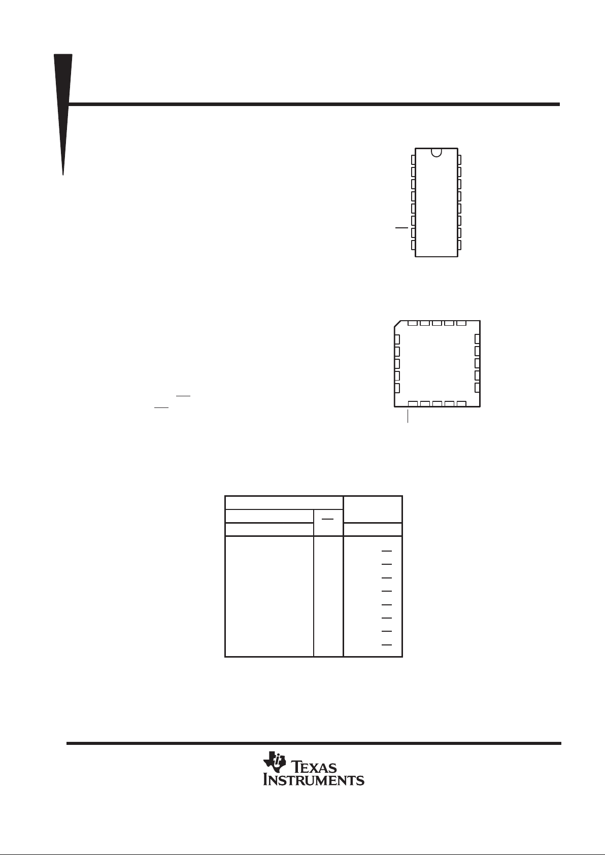
SN54ALS251 ...J PACKAGE
SN74ALS251 ...D OR N PACKAGE
(TOP VIEW)
3212019
910111213
4
5
6
7
8
18
17
16
15
14
D5
D6
NC
D7
A
D1
D0
NC
Y
W
SN54ALS251 . . . FK PACKAGE
(TOP VIEW)
D2D3NC
C
B
D4
OE
GND
NC
NC – No internal connection
V
CC
1
2
3
4
5
6
7
8
16
15
14
13
12
11
10
9
D3
D2
D1
D0
Y
W
OE
GND
V
CC
D4
D5
D6
D7
A
B
C
PRODUCTION DATA information is current as of publication date.
Products conform to specifications per the terms of Texas Instruments
standard warranty. Production processing does not necessarily include
testing of all parameters.
SN54ALS251, SN74ALS251
1-OF-8 DATA SELECTORS/MULTIPLEXERS
WITH 3-STATE OUTPUTS
SDAS215A – APRIL 1982 – REVISED DECEMBER 1994
2
POST OFFICE BOX 655303 • DALLAS, TEXAS 75265
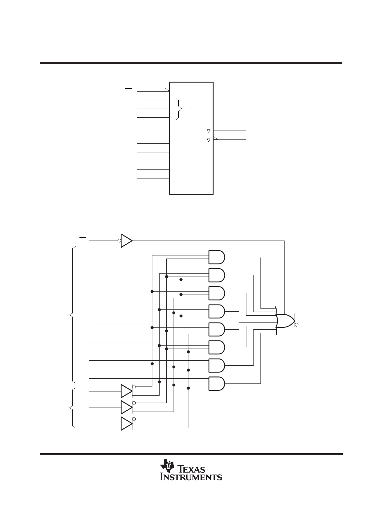
logic symbol
†
MUX
EN
7
0
11
A
10
B
2
9
C
0
4
D0
1
3
D1
2
2
D2
3
1
D3
4
15
D4
5
14
D5
6
13
D6
7
12
D7
0
7
G
W
6
Y
5
OE
†
This symbol is in accordance with ANSI/IEEE Std 91-1984 and IEC Publication 617-12.
Pin numbers shown are for the D, J, and N packages.
logic diagram (positive logic)
7
4
3
2
1
15
14
13
12
11
10
9
5
6
OE
D0
D1
D2
D3
D4
D5
D6
D7
A
B
C
Y
W
Data
Inputs
Data
Select
(binary)
Pin numbers shown are for the D, J, and N packages.
SN54ALS251, SN74ALS251
1-OF-8 DATA SELECTORS/MULTIPLEXERS
WITH 3-STATE OUTPUTS
SDAS215A – APRIL 1982 – REVISED DECEMBER 1994
3
POST OFFICE BOX 655303 • DALLAS, TEXAS 75265
absolute maximum ratings over operating free-air temperature range (unless otherwise noted)
†
Supply voltage, V
CC
7 V. . . . . . . . . . . . . . . . . . . . . . . . . . . . . . . . . . . . . . . . . . . . . . . . . . . . . . . . . . . . . . . . . . . . . . . .
Input voltage, V
I
7 V. . . . . . . . . . . . . . . . . . . . . . . . . . . . . . . . . . . . . . . . . . . . . . . . . . . . . . . . . . . . . . . . . . . . . . . . . . . .
Voltage applied to a disabled 3-state output 5.5 V. . . . . . . . . . . . . . . . . . . . . . . . . . . . . . . . . . . . . . . . . . . . . . . . . .
Operating free-air temperature range, T
A
: SN54ALS251 –55°C to 125°C. . . . . . . . . . . . . . . . . . . . . . . . . . . . .
SN74ALS251 0°C to 70°C. . . . . . . . . . . . . . . . . . . . . . . . . . . . . . . . .
Storage temperature range –65°C to 150°C. . . . . . . . . . . . . . . . . . . . . . . . . . . . . . . . . . . . . . . . . . . . . . . . . . . . . . .
†
Stresses beyond those listed under “absolute maximum ratings” may cause permanent damage to the device. These are stress ratings only, and
functional operation of the device at these or any other conditions beyond those indicated under “recommended operating conditions” is not
implied. Exposure to absolute-maximum-rated conditions for extended periods may affect device reliability.
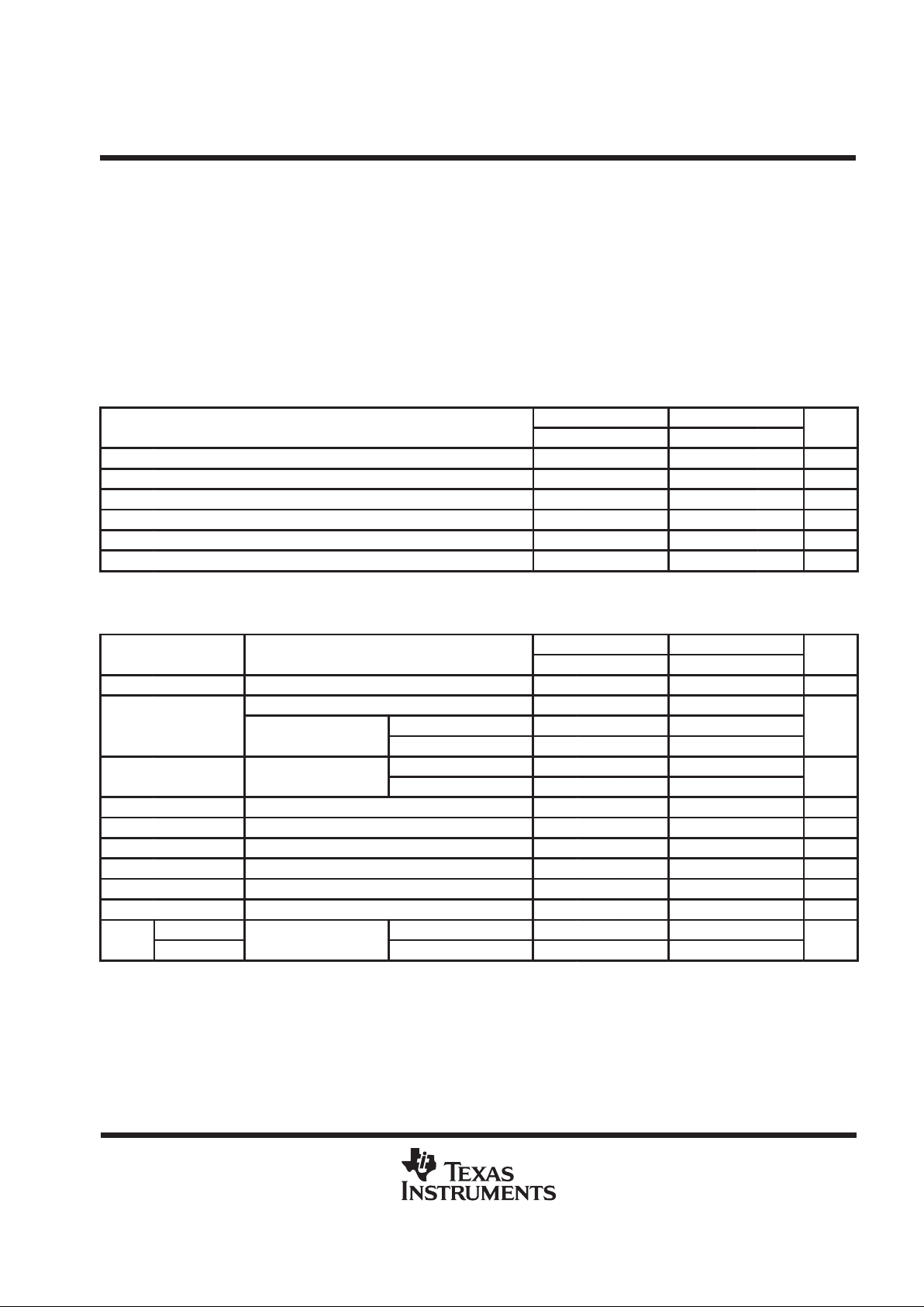
recommended operating conditions
SN54ALS251 SN74ALS251
MIN NOM MAX MIN NOM MAX
UNIT
V
CC
Supply voltage 4.5 5 5.5 4.5 5 5.5 V
V
IH
High-level input voltage 2 2 V
V
IL
Low-level input voltage 0.7 0.8 V
I
OH
High-level output current –1 –2.6 mA
I
OL
Low-level output current 12 24 mA
T
A
Operating free-air temperature –55 125 0 70 °C
electrical characteristics over recommended operating free-air temperature range (unless
otherwise noted)
SN54ALS251 SN74ALS251
PARAMETER
TEST CONDITIONS
MIN TYP‡MAX MIN TYP‡MAX
UNIT
V
IK
VCC = 4.5 V, II = –18 mA –1.5 –1.5 V
VCC = 4.5 V to 5.5 V, IOH = –0.4 mA VCC –2 VCC –2
V
OH
IOH = –1 mA 2.4 3.3
V
V
CC
= 4.5
V
IOH = –2.6 mA 2.4 3.2
IOL = 12 mA 0.25 0.4 0.25 0.4
VOLV
CC
= 4.5
V
IOL = 24 mA 0.35 0.5
V
I
OZH
VCC = 5.5 V, VO = 2.7 V 20 20 µA
I
OZL
VCC = 5.5 V, VO = 0.4 V –20 –20 µA
I
I
VCC = 5.5 V, VI = 7 V 0.1 0.1 mA
I
IH
VCC = 5.5 V, VI = 2.7 V 20 20 µA
I
IL
VCC = 5.5 V, VI = 0.4 V –0.1 –0.1 mA
I
O
§
VCC = 5.5 V, VO = 4.5 V –20 –112 –30 –112 mA
Enabled
Inputs at GND 7 10 7 10
I
CC
Disabled
V
CC
= 5.5
V
Inputs at 4.5 V 9.4 14 9.4 14
mA
‡
All typical values are at VCC = 5 V, TA = 25°C.
§
The output conditions have been chosen to produce a current that closely approximates one half of the true short-circuit output current, IOS.
SN54ALS251, SN74ALS251
1-OF-8 DATA SELECTORS/MULTIPLEXERS
WITH 3-STATE OUTPUTS
SDAS215A – APRIL 1982 – REVISED DECEMBER 1994
4
POST OFFICE BOX 655303 • DALLAS, TEXAS 75265
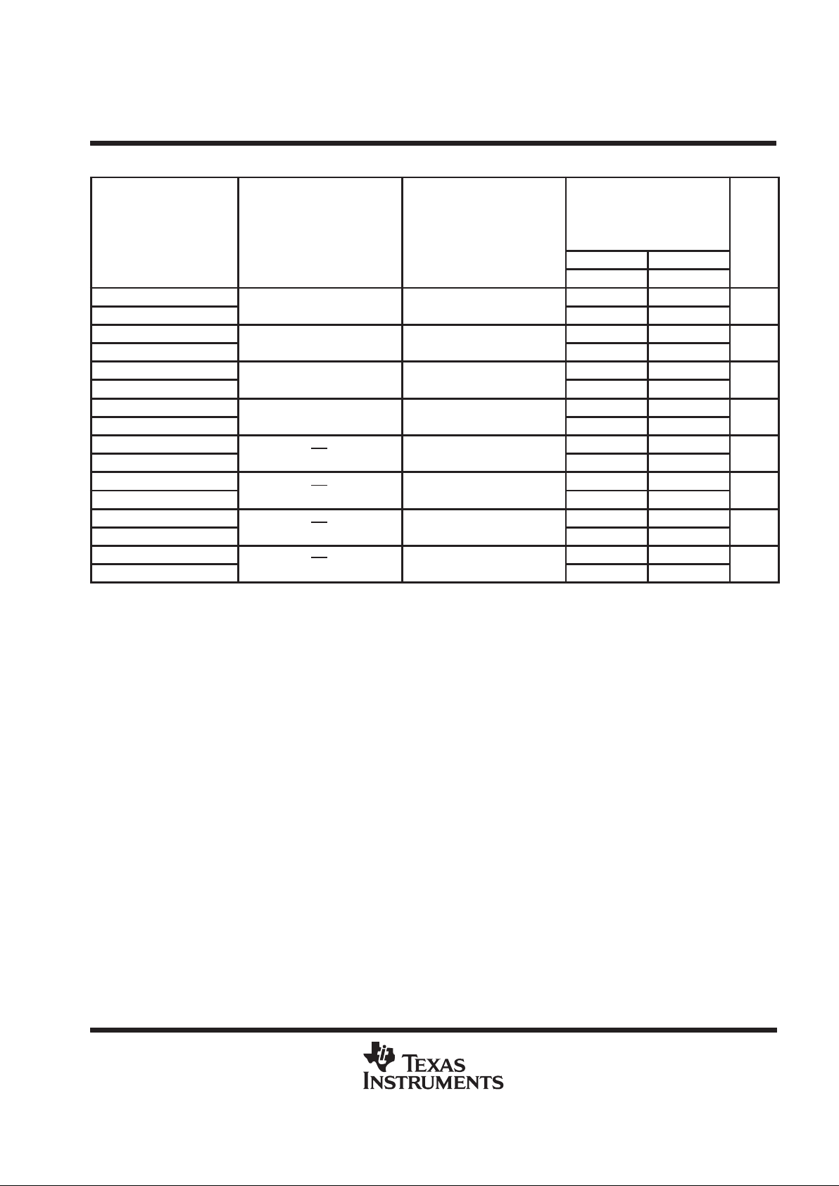
switching characteristics (see Figure 1)
PARAMETER
FROM
(INPUT)
TO
(OUTPUT)
VCC = 4.5 V to 5.5 V,
CL = 50 pF,
R1 = 500 Ω
,
R2 = 500 Ω,
TA = MIN to MAX
†
UNIT
SN54ALS251 SN74ALS251
MIN MAX MIN MAX
t
PLH
1 21 5 18
t
PHL
A, B, or C
Y
7 34 8 24
ns
t
PLH
5 38 8 24
t
PHL
A, B, or C
W
7 26 7 23
ns
t
PLH
2 15 2 10
t
PHL
A
ny
D
Y
3 23 3 15
ns
t
PLH
3 25 3 15
t
PHL
A
ny
D
W
3 20 3 15
ns
t
PZH
3 21 3 15
t
PZL
OE
Y
3 19 3 15
ns
t
PZH
3 21 3 15
t
PZL
OE
W
3 19 3 15
ns
t
PZH
2 12 2 10
t
PZL
OE
Y
1 18 1 10
ns
t
PZH
2 12 2 10
t
PZL
OE
W
1 18 1 10
ns
†
For conditions shown as MIN or MAX, use the appropriate value specified under recommended operating conditions.
SN54ALS251, SN74ALS251
1-OF-8 DATA SELECTORS/MULTIPLEXERS
WITH 3-STATE OUTPUTS
SDAS215A – APRIL 1982 – REVISED DECEMBER 1994
5
POST OFFICE BOX 655303 • DALLAS, TEXAS 75265
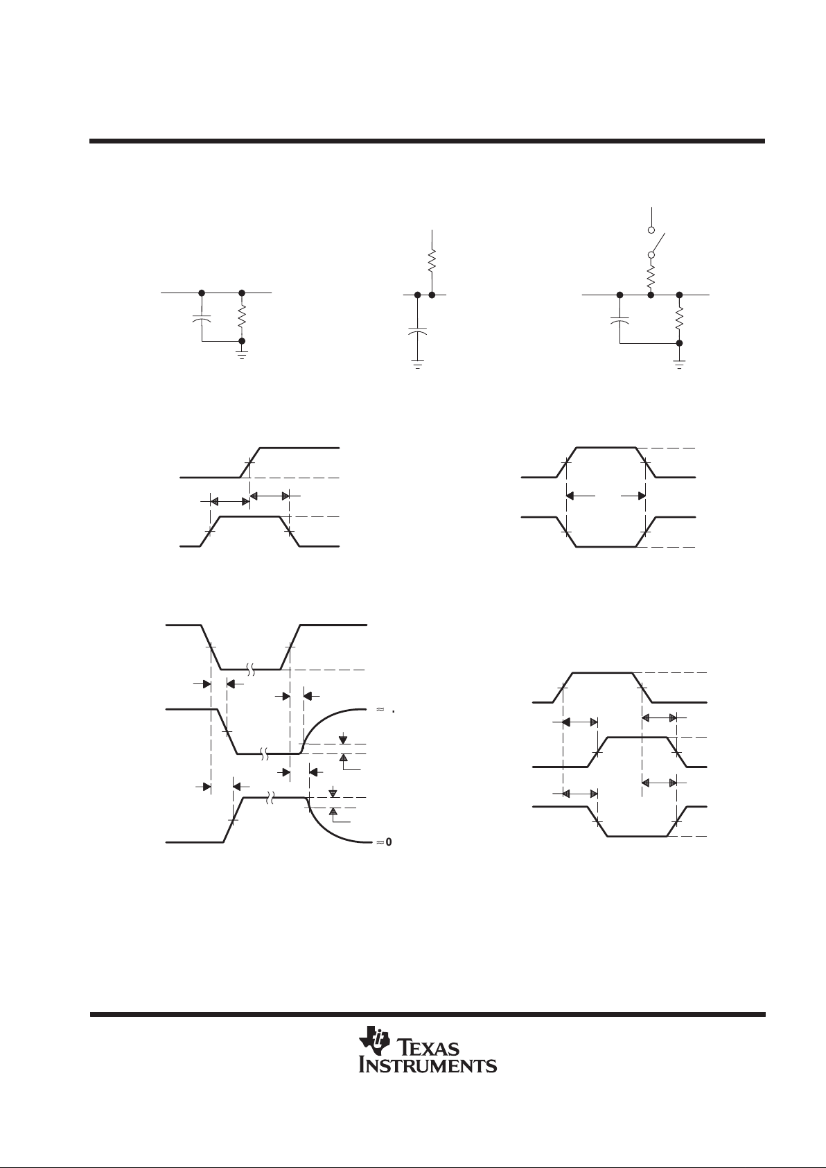
PARAMETER MEASUREMENT INFORMATION
SERIES 54ALS/74ALS AND 54AS/74AS DEVICES
t
PHZ
t
PLZ
t
PHL
t
PLH
0.3 V
t
PZL
t
PZH
t
PLH
t
PHL
LOAD CIRCUIT
FOR 3-STATE OUTPUTS
From Output
Under Test
Test
Point
R1
S1
C
L
(see Note A)
7 V
1.3 V
1.3 V1.3 V
3.5 V
3.5 V
0.3 V
0.3 V
t
h
t
su
VOLTAGE WAVEFORMS
SETUP AND HOLD TIMES
Timing
Input
Data
Input
1.3 V 1.3 V
3.5 V
3.5 V
0.3 V
0.3 V
High-Level
Pulse
Low-Level
Pulse
t
w
VOLTAGE WAVEFORMS
PULSE DURATIONS
Input
Out-of-Phase
Output
(see Note C)
1.3 V 1.3 V
1.3 V1.3 V
1.3 V 1.3 V
1.3 V1.3 V
1.3 V
1.3 V
3.5 V
3.5 V
0.3 V
0.3 V
V
OL
V
OH
V
OH
V
OL
Output
Control
(low-level
enabling)
Waveform 1
S1 Closed
(see Note B)
Waveform 2
S1 Open
(see Note B)
[
0 V
V
OH
V
OL
[
3.5 V
In-Phase
Output
0.3 V
1.3 V 1.3 V
VOLTAGE WAVEFORMS
PROPAGATION DELAY TIMES
VOLTAGE WAVEFORMS
ENABLE AND DISABLE TIMES, 3-STATE OUTPUTS
R2
V
CC
R
L
Test
Point
From Output
Under Test
C
L
(see Note A)
LOAD CIRCUIT
FOR OPEN-COLLECTOR OUTPUTS
LOAD CIRCUIT FOR
BI-STATE
TOTEM-POLE OUTPUTS
From Output
Under Test
Test
Point
C
L
(see Note A)
R
L
RL = R1 = R2
NOTES: A. CL includes probe and jig capacitance.
B. Waveform 1 is for an output with internal conditions such that the output is low except when disabled by the output control.
Waveform 2 is for an output with internal conditions such that the output is high except when disabled by the output control.
C. When measuring propagation delay items of 3-state outputs, switch S1 is open.
D. All input pulses have the following characteristics: PRR ≤ 1 MHz, tr = tf = 2 ns, duty cycle = 50%.
E. The outputs are measured one at a time with one transition per measurement.
Figure 1. Load Circuits and Voltage Waveforms

IMPORTANT NOTICE
T exas Instruments and its subsidiaries (TI) reserve the right to make changes to their products or to discontinue
any product or service without notice, and advise customers to obtain the latest version of relevant information
to verify, before placing orders, that information being relied on is current and complete. All products are sold
subject to the terms and conditions of sale supplied at the time of order acknowledgement, including those
pertaining to warranty, patent infringement, and limitation of liability.
TI warrants performance of its semiconductor products to the specifications applicable at the time of sale in
accordance with TI’s standard warranty. Testing and other quality control techniques are utilized to the extent
TI deems necessary to support this warranty. Specific testing of all parameters of each device is not necessarily
performed, except those mandated by government requirements.
CERT AIN APPLICATIONS USING SEMICONDUCTOR PRODUCTS MAY INVOLVE POTENTIAL RISKS OF
DEATH, PERSONAL INJURY, OR SEVERE PROPERTY OR ENVIRONMENTAL DAMAGE (“CRITICAL
APPLICATIONS”). TI SEMICONDUCTOR PRODUCTS ARE NOT DESIGNED, AUTHORIZED, OR
WARRANTED TO BE SUITABLE FOR USE IN LIFE-SUPPORT DEVICES OR SYSTEMS OR OTHER
CRITICAL APPLICATIONS. INCLUSION OF TI PRODUCTS IN SUCH APPLICA TIONS IS UNDERST OOD TO
BE FULLY AT THE CUSTOMER’S RISK.
In order to minimize risks associated with the customer’s applications, adequate design and operating
safeguards must be provided by the customer to minimize inherent or procedural hazards.
TI assumes no liability for applications assistance or customer product design. TI does not warrant or represent
that any license, either express or implied, is granted under any patent right, copyright, mask work right, or other
intellectual property right of TI covering or relating to any combination, machine, or process in which such
semiconductor products or services might be or are used. TI’s publication of information regarding any third
party’s products or services does not constitute TI’s approval, warranty or endorsement thereof.
Copyright 1998, Texas Instruments Incorporated
 Loading...