

Texas Instruments SN54ABT8996FK, SN54ABT8996JT, SN74ABT8996DWR, SN74ABT8996PWLE, SN74ABT8996PWR Datasheet
...
SN54ABT8996, SN74ABT8996
10-BIT ADDRESSABLE SCAN PORTS
MULTIDROP-ADDRESSABLE IEEE STD 1149.1 (JTAG) TAP TRANSCEIVERS
SCBS489C – AUGUST 1994 – REVISED APRIL 1999
1
POST OFFICE BOX 655303 • DALLAS, TEXAS 75265
D
Members of Texas Instruments Broad
Family of Testability Products Supporting
IEEE Std 1149.1-1990 (JTAG) Test Access
Port (TAP) and Boundary-Scan Architecture
D
Extend Scan Access From Board Level to
Higher Levels of System Integration
D
Promote Reuse of Lower-Level
(Chip/Board) Tests in System Environment
D
Switch-Based Architecture Allows Direct
Connect of Primary TAP to Secondary TAP
D
Primary TAP Is Multidrop for Minimal Use of
Backplane Wiring Channels
D
Simple Addressing (Shadow) Protocol Is
Received/Acknowledged on Primary TAP
D
Shadow Protocols Can Occur in Any of
Test-Logic-Reset, Run-Test/Idle, Pause-DR,
and Pause-IR TAP States to Provide for
Board-to-Board Test and Built-In Self-Test
D
10-Bit Address Space Provides for Up to
1021 User-Specified Board Addresses
D
Bypass (BYP) Pin Forces
Primary-to-Secondary Connection Without
Use of Shadow Protocols
D
Connect (CON) Pin Provides Indication of
Primary-to-Secondary Connection
D
High-Drive Outputs (–32-mA IOH, 64-mA IOL)
Support Backplane Interface at Primary and
High Fanout at Secondary
D
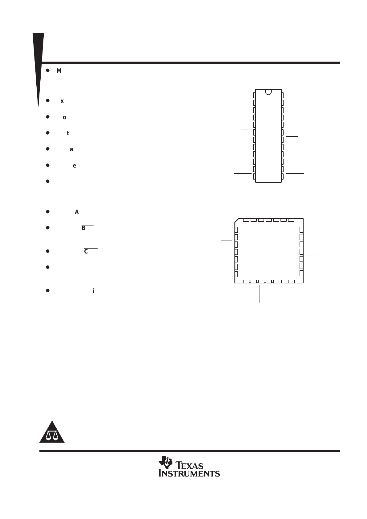
Package Options Include Plastic SmallOutline (DW) and Thin Shrink SmallOutline (PW) Packages, Ceramic Chip
Carriers (FK), and Ceramic DIPs (JT)
description
The ’ABT8996 10-bit addressable scan ports (ASP) are members of the Texas Instruments (TI) SCOPE
testability integrated-circuit family . This family of devices supports IEEE Standard 1 149.1-1990 boundary scan
to facilitate testing of complex circuit assemblies. Unlike most SCOPE devices, the ASP is not a
boundary-scannable device, rather, it applies TI’ s addressable-shadow-port technology to the IEEE Standard
1149.1-1990 (JTAG) test access port (TAP) to extend scan access beyond the board level.
Conceptually, the ASP is a simple switch that can be used to directly connect a set of multidrop primary TAP
signals to a set of secondary TAP signals – for example, to interface backplane TAP signals to a board-level
TAP. The ASP provides all signal buffering that might be required at these two interfaces. When primary and
secondary TAPs are connected, only a moderate propagation delay is introduced – no storage/retiming
elements are inserted. This minimizes the need for reformatting board-level test vectors for in-system use.
Copyright 1999, Texas Instruments Incorporated
PRODUCTION DATA information is current as of publication date.
Products conform to specifications per the terms of Texas Instruments
standard warranty. Production processing does not necessarily include
testing of all parameters.
Please be aware that an important notice concerning availability, standard warranty, and use in critical applications of
Texas Instruments semiconductor products and disclaimers thereto appears at the end of this data sheet.
SCOPE is a trademark of Texas Instruments Incorporated.
17
SN54ABT8996 . . . JT PACKAGE
SN74ABT8996 . . . DW OR PW PACKAGE
(TOP VIEW)
5
6
7
8
9
10
11
25
24
23
22
21
20
19
432128
12 13 14 15 16
A8
A9
V
CC
NC
CON
STDI
STCK
A1
A0
BYP
NC
GND
PTDO
PTCK
SN54ABT8996 . . . FK PACKAGE
(TOP VIEW)
A2A3A4
STRST
STDO
PTDI
PTRST
NC
NC
A6
A7
A5
PTMS
STMS
18
27 26
A4
A3
A2
A1
A0
BYP
GND
PTDO
PTCK
PTMS
PTDI
PTRST
A5
A6
A7
A8
A9
V
CC
CON
STDI
STCK
STMS
STDO
STRST
1
2
3
4
5
6
7
8
9
10
11
12
24
23
22
21
20
19
18
17
16
15
14
13
NC – No internal connection

SN54ABT8996, SN74ABT8996
10-BIT ADDRESSABLE SCAN PORTS
MULTIDROP-ADDRESSABLE IEEE STD 1149.1 (JTAG) TAP TRANSCEIVERS
SCBS489C – AUGUST 1994 – REVISED APRIL 1999
2
POST OFFICE BOX 655303 • DALLAS, TEXAS 75265
description (continued)
Most operations of the ASP are synchronous to the primary test clock (PTCK) input. This PTCK signal always
is buffered directly onto the secondary test clock (STCK) output.
Upon power up of the device, the ASP assumes a condition in which the primary T AP is disconnected from the
secondary TAP (unless the bypass signal is used, as below). This reset condition also can be entered by the
assertion of the primary test reset (PTRST
) input or by use of shadow protocol. The PTRST signal is always
buffered directly onto the secondary test reset (STRST
) output, ensuring that the ASP and its associated
secondary TAP can be reset simultaneously.
When connected, the primary test data input (PTDI) and primary test mode select (PTMS) input are buffered
onto the secondary test data output (STDO) and secondary test mode select (STMS) output, respectively , while
the secondary test data input (STDI) is buffered onto the primary test data output (PTDO). When disconnected,
STDO is at high impedance, while PTDO is at high impedance, except during acknowledgement of a shadow
protocol. Upon disconnect of the secondary T AP, STMS holds its last low or high level, allowing the secondary
T AP to be held in its last stable state. Upon reset of the ASP, STMS is high, allowing the secondary TAP to be
synchronously reset to the Test-Logic-Reset state.
In system, primary-to-secondary connection is based on shadow protocols that are received and acknowledged
on PTDI and PTDO, respectively . These protocols can occur in any of the stable T AP states other than Shift-DR
or Shift-IR (i.e., T est-Logic-Reset, Run-T est/Idle, Pause-DR or Pause-IR). The essential nature of the protocols
is to receive/transmit an address via a serial bit-pair signaling scheme. When an address is received serially
at PTDI that matches that at the parallel address inputs (A9–A0), the ASP serially retransmits its address at
PTDO as an acknowledgement and then assumes the connected (ON) status, as above. If the received address
does not match that at the address inputs, the ASP immediately assumes the disconnected (OFF) status without
acknowledgement.
The ASP also supports three dedicated addresses that can be received globally (that is, to which all ASPs
respond) during shadow protocols. Receipt of the dedicated disconnect address (DSA) causes the ASP to
disconnect in the same fashion as a non-matching address. Reservation of this address for global use ensures
that at least one address is available to disconnect all receiving ASPs. The DSA is especially useful when the
secondary TAPs of multiple ASPs are to be left in different stable states. Receipt of the reset address (RSA)
causes the ASP to assume the reset condition, as above. Receipt of the test-synchronization address (TSA)
causes the ASP to assume a connect status (MULTICAST) in which PTDO is at high impedance but the
connections from PTMS to STMS and PTDI to STDO are maintained to allow simultaneous operation of the
secondary T APs of multiple ASPs. This is useful for multicast TAP-state movement, simultaneous test operation
(such as in Run-Test/Idle state), and scanning of common test data into multiple like scan chains. The TSA is
valid only when received in the Pause-DR or Pause-IR TAP states.
Alternatively , primary-to-secondary connection can be selected by assertion of a low level at the bypass (BYP
)
input. This operation is asynchronous to PTCK and is independent of PTRST
and/or power-up reset. This
bypassing feature is especially useful in the board-test environment, since it allows the board-level automated
test equipment (A TE) to treat the ASP as a simple transceiver. When the BYP
input is high, the ASP is free to
respond to shadow protocols. Otherwise, when BYP
is low, shadow protocols are ignored.
Whether the connected status is achieved by use of shadow protocol or by use of BYP
, this status is indicated
by a low level at the connect (CON
) output. Likewise, when the secondary T AP is disconnected from the primary
TAP, the CON
output is high.
The SN54ABT8996 is characterized for operation over the full military temperature range of –55°C to 125°C.
The SN74ABT8996 is characterized for operation from –40°C to 85°C.
SN54ABT8996, SN74ABT8996
10-BIT ADDRESSABLE SCAN PORTS
MULTIDROP-ADDRESSABLE IEEE STD 1149.1 (JTAG) TAP TRANSCEIVERS
SCBS489C – AUGUST 1994 – REVISED APRIL 1999
3
POST OFFICE BOX 655303 • DALLAS, TEXAS 75265
FUNCTION TABLE
INPUTS
SHADOW-PROTOCOL
OUTPUTS
PRIMARY-TO-SECONDARY
BYP PTRST
RESULT
†
STRST STCK STMS STDO PTDO CON
CONNECT STATUS
L L — L PTCK H
‡
PTDI STDI L BYP/TRST
‡
L H—HPTCK PTMS PTDI STDI L BYP
H L—LPTCK H Z Z H TRST
H H RESET H PTCK H Z Z H RESET
H H MATCH H PTCK PTMS PTDI STDI L ON
H H NO MATCH H PTCK STMS
0
§
Z Z H OFF
H H HARD ERROR
¶
H PTCK STMS
0
§
Z Z H OFF
H H DISCONNECT H PTCK STMS
0
§
Z Z H OFF
H H TEST SYNCHRONIZATION H PTCK PTMS PTDI Z L MULTICAST
†
Shadow protocols are received serially via PTCK and PTDI and acknowledged serially via PTCK and PTDO under certain conditions in which
PTMS is static low or static high (see shadow protocol). The result shown here follows any required acknowledgement.
‡
In normal operation of IEEE Std 1149.1-compliant architectures, it is recommended that TMS be high prior to release of TRST
. The BYP/TRST
connect status ensures that this condition is met at STMS regardless of the applied PTMS. Also, it is recommended that STMS be kept high for
a minimum duration of 5 PTCK cycles following assertion of PTRST
, either by maintaining PTRST low or by setting PTMS high. This ensures
that ICs both with and without TRST
inputs are moved to their T est-Logic-Reset T AP states. It is expected that in normal application, this condition
will only occur when BYP
is fixed at the low state. In such case, upon release of PTRST , the ASP immediately resumes the BYP connect status.
§
STMS level before indicated steady-state conditions were established
¶
The shadow protocol is well defined. Some variations in the protocol are tolerated (see protocol errors). Those that are not tolerated are
considered hard errors and cause disconnect as indicated.
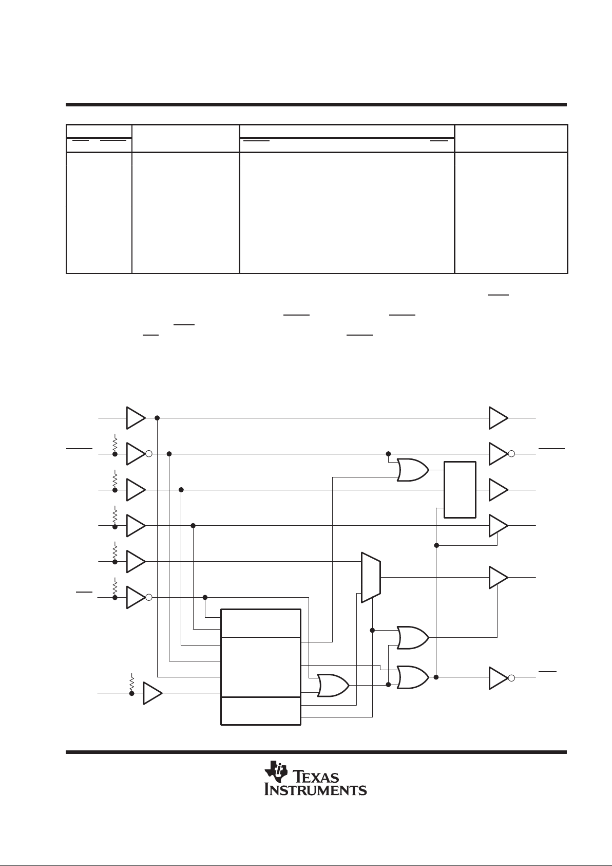
functional block diagram
CON
Shadow-Protocol
Receive
1D
PTCK
PTRST
V
CC
STCK
STRST
STMSPTMS
V
CC
PTDI
V
CC
STDO
STDI
V
CC
PTDO
BYP
V
CC
A9–A0
V
CC
Connect Control
Shadow-Protocol
Transmit
C1
S
9
12
10
11
17
6
16
13
15
14
8
18
Pin numbers shown are for the DW, JT, and PW packages.
20–24,
1–5

SN54ABT8996, SN74ABT8996
10-BIT ADDRESSABLE SCAN PORTS
MULTIDROP-ADDRESSABLE IEEE STD 1149.1 (JTAG) TAP TRANSCEIVERS
SCBS489C – AUGUST 1994 – REVISED APRIL 1999
4
POST OFFICE BOX 655303 • DALLAS, TEXAS 75265
Terminal Functions
TERMINAL
NAME
DESCRIPTION
A9–A0
Address inputs. The ASP compares addresses received via shadow protocol against the value at A9–A0 to determine
address match. The bit order is from most significant to least significant. An internal pullup at each A9–A0 terminal forces
the terminal to a high level if it has no external connection.
BYP
Bypass input. A low input at BYP forces the ASP into BYP or BYP/TRST status, depending on PTRST being high or
low, respectively. While BYP
is low, shadow protocols are ignored. Otherwise, while BYP is high, the ASP is free to
respond to shadow protocols. An internal pullup forces BYP
to a high level if it has no external connection.
CON
Connect indicator (output). The ASP indicates secondary-scan-port activity (resulting from BYP, BYP/TRST,
MULTICAST, or ON status) by forcing CON
to be low. Inactivity (resulting from OFF , RESET , or TRST status) is indicated
when CON
is high.
GND Ground
PTCK
Primary test clock. PTCK receives the TCK signal required by IEEE Standard 1149.1-1990. The ASP always buffers
PTCK to STCK. Shadow protocols are received/acknowledged synchronously to PTCK and connect-status changes
invoked by shadow protocol are made synchronously to PTCK.
PTDI
Primary test data input. PTDI receives the TDI signal required by IEEE Standard 1 149.1-1990. During appropriate T AP
states, the ASP monitors PTDI for shadow protocols. During shadow protocols, data at PTDI is captured on the rising
edge of PTCK. When a valid shadow protocol is received in this fashion, the ASP compares the received address against
the A9–A0 inputs. If the ASP detects a match, it outputs an acknowledgement and then connects its primary TAP
terminals to its secondary T AP terminals. Under BYP , BYP/TRST, MULTICAST or ON status, the ASP buffers the PTDI
signal to STDO. An internal pullup forces PTDI to a high level if it has no external connection.
PTDO
Primary test data output. PTDO transmits the TDO signal required by IEEE Standard 1149.1-1990. During shadow
protocols, the ASP transmits any required acknowledgement via the PTDO. The acknowledgement data output at PTDO
changes on the falling edge of PTCK. Under BYP , BYP/TRST , or ON status, the ASP buffers the PTDO signal from STDI.
Under OFF, MUL TICAST, RESET, or TRST status, PTDO is at high impedance.
PTMS
Primary test mode select. PTMS receives the TMS signal required by IEEE Standard 1149.1-1990. The ASP monitors
the PTMS to determine the TAP-controller state. During stable TAP states other than Shift-DR or Shift-IR (i.e.,
Test-Logic-Reset, Run-Test-Idle, Pause-DR, Pause-IR) the ASP can respond to shadow protocols. Under BYP,
MULTICAST, or ON status, the ASP buffers the PTMS signal to STMS. An internal pullup forces PTMS to a high level
if it has no external connection.
PTRST
Primary test reset. PTRST receives the TRST signal allowed by IEEE Standard 1149.1-1990. The ASP always buf fers
PTRST
to STRST . A low input at PTRST forces the ASP to assume TRST or BYP/TRST status, depending on BYP being
high or low, respectively. Such operation also asynchronously resets the internal ASP state to its power-up condition.
Otherwise, while PTRST
is high, the ASP is free to respond to shadow protocols. An internal pullup forces PTRST to
a high level if it has no external connection.
STCK
Secondary test clock. STCK retransmits the TCK signal required by IEEE Standard 1149.1-1990. The ASP always
buffers STCK from PTCK.
STDI
Secondary test data input. STDI receives the TDI signal required by IEEE Standard 1149.1-1990. Under BYP,
BYP/TRST , or ON status, the ASP buffers STDI to PTDO. An internal pullup forces STDI to a high level if it has no external
connection.
STDO
Secondary test data output. STDO transmits the TDO signal required by IEEE Standard 1149.1-1990. Under BYP,
BYP/TRST , MUL TICAST, or ON status, the ASP buffers STDO from PTDI. Under OFF, RESET, or TRST status, STDO
is at high impedance.
STMS
Secondary test mode select. STMS retransmits the TMS signal required by IEEE Standard 1149.1-1990. Under BYP,
MULTICAST, or ON status, the ASP buffers STMS from PTMS. When disconnected (as a result of OFF status), STMS
maintains its last valid state until the ASP assumes BYP/TRST, RESET, or TRST status (upon which it is forced high)
or the ASP again assumes BYP, MULTICAST, or ON status.
STRST
Secondary test reset. STRST retransmits the TRST signal allowed by IEEE Standard 1149.1-1990. The ASP always
buffers STRST
from PTRST.
V
CC
Supply voltage
SN54ABT8996, SN74ABT8996
10-BIT ADDRESSABLE SCAN PORTS
MULTIDROP-ADDRESSABLE IEEE STD 1149.1 (JTAG) TAP TRANSCEIVERS
SCBS489C – AUGUST 1994 – REVISED APRIL 1999
5
POST OFFICE BOX 655303 • DALLAS, TEXAS 75265
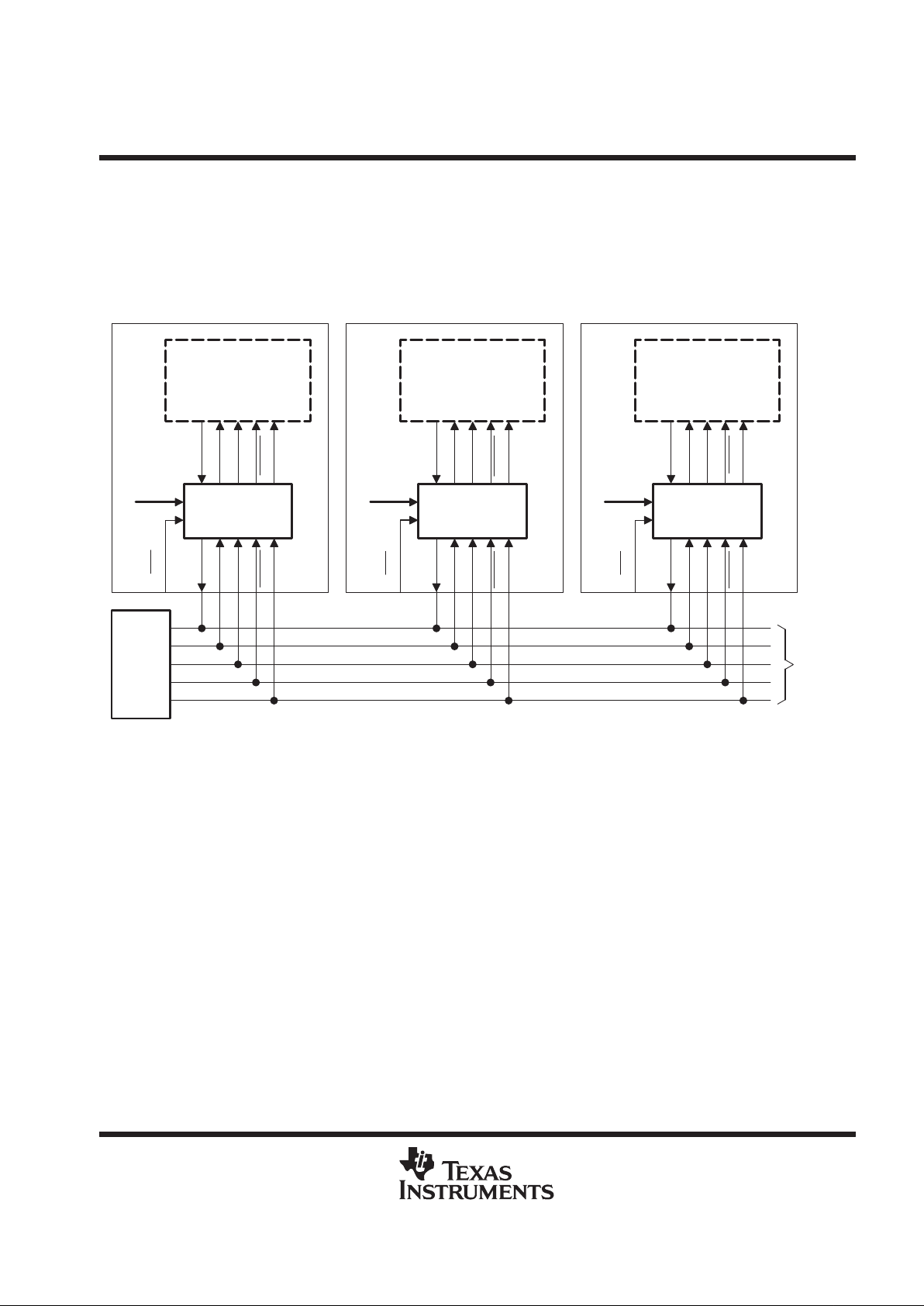
application information
In application, the ASP is used at each of several (serially-chained) groups of IEEE Std 1149.1-compliant
devices. The ASP for each such group is assigned an address (via inputs A9–A0) that is unique from that
assigned to ASPs for the remaining groups. Each ASP is wired at its primary T AP to common (multidrop) TAP
signals (sourced from a central IEEE Std 1149.1 bus master) and fans out its secondary TAP signals to the
specific group of IEEE Std 1149.1-compliant devices with which it is associated. An example is shown in
Figure 1.
ASP
IEEE Std 1149.1-
Compliant
Device Chain
PTRST
PTDI
PTMS
PTCK
PTDO
STRST
STDO
STMS
STCK
STDI
ADDR1
A9–A0
ASP
IEEE Std 1149.1-
Compliant
Device Chain
PTRST
PTDI
PTMS
PTCK
PTDO
STRST
STDO
STMS
STCK
STDI
ADDR2
A9–A0
ASP
IEEE Std 1149.1-
Compliant
Device Chain
PTRST
PTDI
PTMS
PTCK
PTDO
STRST
STDO
STMS
STCK
STDI
ADDR3
A9–A0
TRST
TDO
TMS
TCK
TDI
IEEE
Std
1149.1
Bus
Master
To
Other
Modules
BYP
BYP
BYP
Figure 1. ASP Application
This application allows the ASP to be wired to a 4- or 5-wire multidrop test access bus, such as might be found
on a backplane. Each ASP would then be located on a module, for example a printed-circuit board (PCB), which
contains a serial chain of IEEE Std 1 149.1-compliant devices and which would plug into the module-to-module
bus (e.g., backplane). In the complete system, the ASP shadow protocols would allow the selection of the scan
chain on a single module. The selected scan chain could then be controlled, via the multidrop T AP, as if it were
the only scan chain in the system. Normal IR and DR scans can then be performed to accomplish the module
test objectives.
Once scan operations to a given module are complete, another module can be selected in the same fashion,
at which time the ASP-based connection to the first module is dissolved. This procedure can be continued
progressively for each module to be tested. Finally , one of two global addresses can be issued to either leave
all modules unselected (disconnect address, DSA) or to deselect and reset scan chains for all modules (reset
address, RSA).
Additionally , in Pause-DR and Pause-IR TAP states, a third global address (test-synchronization address, TSA)
can be invoked to allow simultaneous T AP-state changes and multicast scan-in operations to selected modules.
This is especially useful in the former case, for allowing selected modules to be moved simultaneously to the
Run-T est-Idle T AP state for module-level or module-to-module built-in self-test (BIST) functions, which operate
synchronously to TCK in that T AP state, and in the latter case, for scanning common test setup/data into multiple
like modules.
SN54ABT8996, SN74ABT8996
10-BIT ADDRESSABLE SCAN PORTS
MULTIDROP-ADDRESSABLE IEEE STD 1149.1 (JTAG) TAP TRANSCEIVERS
SCBS489C – AUGUST 1994 – REVISED APRIL 1999
6
POST OFFICE BOX 655303 • DALLAS, TEXAS 75265
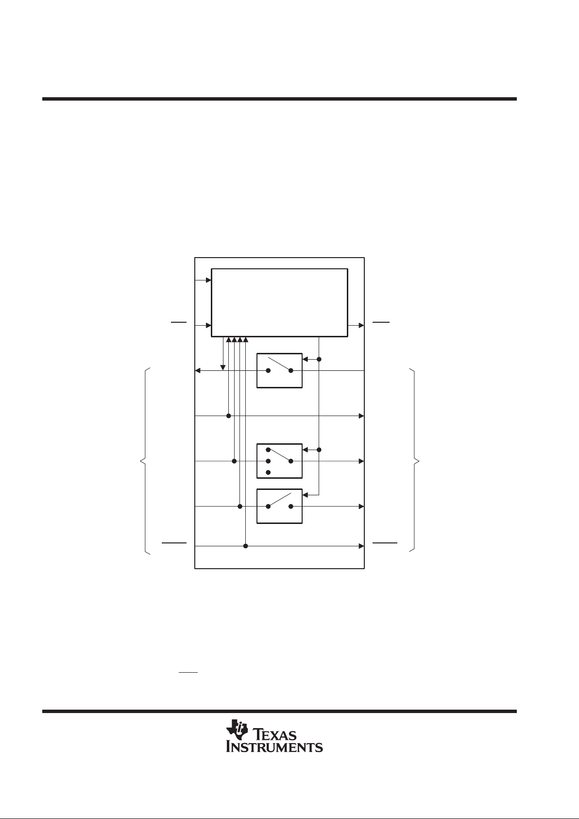
architecture
Conceptually, the ASP can be viewed as a bank of switches that can connect or isolate a module-level TAP
to/from a higher-level (e.g., module-to-module) T AP. This is shown in Figure 2. The state of the switches (open
versus closed) is based on shadow protocols, which are received on PTDI and are synchronous to PTCK.
The simple architecture of the ASP allows the system designer to overcome the limitations of IEEE Std 1 149.1
ring
and
star
configurations. Ring configurations (in which each module’s TDO is chained to the next module’s
TDI) are of limited use in backplane environments, since removal of a module breaks the scan chain and
prevents test of the remainder of the system. Star configurations (in which all module TDOs and TDIs are
connected in parallel) are suited to the backplane environment, but, since each module must receive its own
TMS, are costly in terms of backplane routing channels. By comparison, use of the ASP allows all five IEEE
Std 1149.1 signals to be routed in multidrop fashion.
1
0
Control
CON
STDI
STCK
STMS
STDO
STRST
PTDO
PTCK
PTMS
PTDI
PTRST
BYP
A9–A0
From Multidrop,
Module-to-Module
Test Access Port
To Module-Level
Test Access Port
Figure 2. ASP Conceptual Model
As shown in the functional block diagram, the ASP comprises three major logic blocks. Blocks for
shadow-protocol receive and shadow-protocol transmit are responsible for receipt of select protocol and
transmission of acknowledge protocol, respectively. The connect-control block is responsible for TAP-state
monitor and address matching.
Some additional logic is illustrated outside of these major blocks. This additional logic is responsible for
controlling the activity of the ASP outputs based on the shadow-protocol result and/or protocol bypass [as
selected by an active (low) BYP
input].
SN54ABT8996, SN74ABT8996
10-BIT ADDRESSABLE SCAN PORTS
MULTIDROP-ADDRESSABLE IEEE STD 1149.1 (JTAG) TAP TRANSCEIVERS
SCBS489C – AUGUST 1994 – REVISED APRIL 1999
7
POST OFFICE BOX 655303 • DALLAS, TEXAS 75265
shadow protocol
Addressing of an ASP in system is accomplished by shadow protocols, which are received at PTDI
synchronously to PTCK. Shadow protocols can occur only in the following stable T AP states: T est-Logic-Reset,
Run-Test/Idle, Pause-DR, and Pause-IR. Shadow protocols never occur in Shift-DR or Shift-IR states in order
to prevent contention on the signal bus to which PTDO is wired. Additionally, the ASP PTMS must be held at
a constant low or high level throughout a shadow protocol. If T AP-state changes occur in the midst of a shadow
protocol, the shadow protocol is aborted and the select-protocol state machine returns to its initial state.
The shadow protocol is based on a serial bit-pair signaling scheme in which two bit-pair combinations (data one,
data zero) are used to represent address data and the other two bit-pair combinations (select, idle) are used
for framing – that is, to indicate where address data begins and ends.
These bit pairs are received serially at PTDI (or transmitted serially at PTDO) synchronously to PTCK as follows:
– The idle bit pair (I) is represented as two consecutive high signals.
– The select bit pair (S) is represented as two consecutive low signals.
– The data-one bit pair (D) is represented as a low signal followed by a high signal.
– The data-zero bit pair (D) is represented as a high signal followed by a low signal.
PTCK
PTDI
or
PTDO
First Bit of Pair Is Transmitted
First Bit of Pair Is Received
Second Bit of Pair Is Transmitted
Second Bit of Pair Is Received
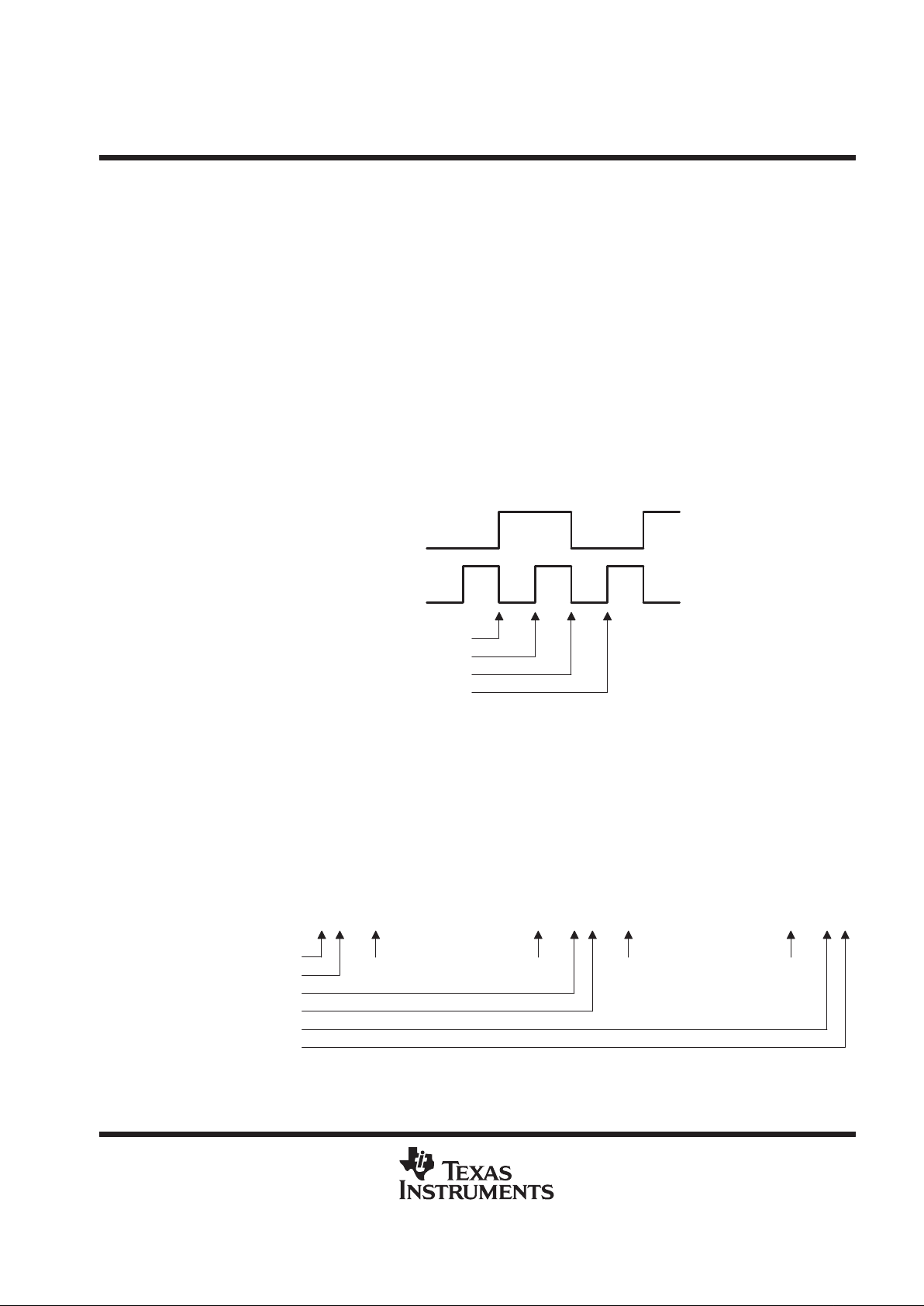
Figure 3. Bit-Pair Timing (Data Zero Shown)
A complete shadow protocol is composed of the receipt of a select protocol followed, if applicable, by the
transmission of an acknowledge protocol (which is issued from PTDO only if the received address matches that
at the A9–A0 inputs). Both of these subprotocols are composed of ten data bit pairs framed at the beginning
by idle and select bit pairs and at the end by select and idle bit pairs. This is represented in an abbreviated
fashion as follows: ISDDDDDDDDDDSI. Figure 4 shows a complete shadow protocol (the symbol T is used to
represent a high-impedance condition on the associated signal line – since the high-impedance state at PTDI
is logically high due to pullup, it maps onto the idle bit pair).
T I S D D D D D D D D D D S I T T T T T T T T T T T T T T T
T T T T T T T T T T T T T T T I S D D D D D D D D D D S I T
Received at PTDI
Transmitted at PTDO
Primary Tap Is Inactive
Select Protocol Begins
Select Protocol Ends
Acknowledge Protocol Begins
Acknowledge Protocol Ends
Primary-to-Secondary Connect,
Scan Operations Can Be Initiated
LSB MSB LSB MSB
Figure 4. Complete Shadow Protocol

SN54ABT8996, SN74ABT8996
10-BIT ADDRESSABLE SCAN PORTS
MULTIDROP-ADDRESSABLE IEEE STD 1149.1 (JTAG) TAP TRANSCEIVERS
SCBS489C – AUGUST 1994 – REVISED APRIL 1999
8
POST OFFICE BOX 655303 • DALLAS, TEXAS 75265
select protocol
The select protocol is the ASP’s means of receiving (at PTDI) address information from an IEEE Std 1 149.1 bus
master. It follows the ISDDDDDDDDDDSI sequence described previously. A 10-bit address value is decoded
from the received data-one and/or data-zero bit pairs. These bit pairs are interpreted in least-significant-bit-first
order (that is, the first data bit pair received is considered to correspond to A0).
acknowledge protocol
Following the receipt of a complete select-protocol sequence, the protocol result provisionally is set to NO
MA TCH and the connect status set to OFF. The received address is then compared to that at the ASP address
inputs (A9–A0). If these address values match, the ASP immediately (with no delay) responds with an
acknowledge protocol transmitted from PTDO. This protocol follows the ISDDDDDDDDDDSI sequence
described previously . The transmitted address represents the address of the selected ASP which, by definition,
is the same address the ASP received in the select protocol. The 10-bit address value is encoded into data-one
and/or data-zero bit pairs. The bit pairs are to be interpreted in least-significant-bit-first order (that is, the first
data bit pair transmitted is to be considered to correspond to A0). If the received address does not match that
at the A9–A0 inputs, no acknowledge protocol is transmitted and the shadow protocol is considered complete.
protocol errors
Protocol errors occur when bit pairs are received out of sequence. Some of these sequencing errors can be
tolerated and are termed
soft
errors. No specific action occurs as the result of a soft error. Other errors represent
cases where the addressing information could be incorrectly received and are termed
hard
errors. Hard errors
are characterized by sequences in which at least one bit of address data has been properly transmitted followed
by a sequencing error. When a hard error occurs, any connection to an ASP is dissolved.
Table 1 lists the bit-pair sequences that result in soft errors and hard errors. A hard error also results when the
primary T AP state changes during select protocol following the proper transmission of at least one bit of address
data. Figures 16 and 17 show shadow-protocol timing in case of protocol hard error while Figure 18 shows
shadow-protocol timing in case of protocol soft error.
T able 1. Shadow-Protocol Errors
†
SOFT ERRORS HARD ERRORS
I(D)I
I(D)(S)I
I(D)(S)(D)I
IS(D)I
I(S)I
IS(D)S(D)I
IS(D
)S(S)
I
IS(S)(D)I
IS(D)S(S)I
IS(S)(D)(S)I
†
A bit-pair token in parentheses
represents one or more instances.
long address
Receipt of an address longer than ten bits is considered a hard error and the ASP assumes OFF status. The
sole exceptions are when all data ones are received or all data zeros are received. In these special cases, the
global addresses represented by these bit sequences are observed and appropriate action taken. That is, in
the case that only data ones (ten or more) are received, the shadow-protocol result is TEST
SYNCHRONIZA TION (if the primary T AP state is Pause-DR or Pause-IR), and in the case that only data zeros
(ten or more) are received, the shadow-protocol result is RESET (see test-synchronization address and reset
address).
short address
In all cases, receipt of an address shorter than ten bits is considered a hard error and the ASP assumes
OFF status.
SN54ABT8996, SN74ABT8996
10-BIT ADDRESSABLE SCAN PORTS
MULTIDROP-ADDRESSABLE IEEE STD 1149.1 (JTAG) TAP TRANSCEIVERS
SCBS489C – AUGUST 1994 – REVISED APRIL 1999
9
POST OFFICE BOX 655303 • DALLAS, TEXAS 75265
connect control
The connect-control block monitors the primary T AP state to enable receipt/acknowledge of shadow protocols
in appropriate states (namely, the stable, non-Shift TAP states: Test-Logic-Reset, Run-Test/Idle, Pause-DR,
and Pause-IR). Upon receipt of a valid shadow protocol, this block performs the address matching required to
compute the shadow-protocol result.
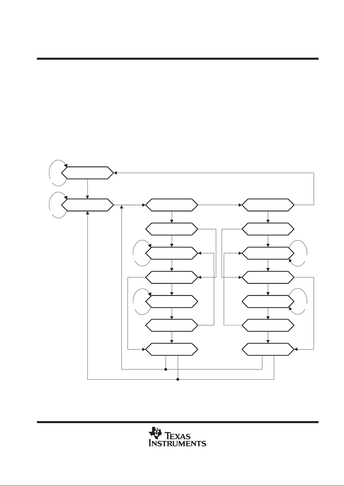
T AP-state monitor
The TAP-state monitor is a synchronous finite-state machine that monitors the primary TAP state. The state
diagram is shown in Figure 5 and mirrors that specified by IEEE Standard 1 149.1-1990. The T AP-state monitor
proceeds through its states based on the level of PTMS at the rising edge of PTCK. Each state is described both
in terms of its significance for ASP devices and for connected IEEE Std 1149.1-compliant devices (called
targets). However, the monitor state (primary TAP) can be different from that of disconnected scan chains
(secondary TAP).
Test-Logic-Reset
Run-Test/Idle Select-DR-Scan
Capture-DR
Shift-DR
Exit1-DR
Pause-DR
Update-DR
PTMS = L
PTMS = L
PTMS = H
PTMS = L
PTMS = H
PTMS = H
PTMS = LPTMS = H
PTMS = L
PTMS = L
PTMS = H
PTMS = L
Exit2-DR
Select-IR-Scan
Capture-IR
Shift-IR
Exit1-IR
Pause-IR
Update-IR
PTMS = L
PTMS = L
PTMS = H
PTMS = L
PTMS = H
PTMS = H
PTMS = LPTMS = H
PTMS = L
Exit2-IR
PTMS = L
PTMS = H PTMS = H
PTMS = H
PTMS = L
PTMS =HPTMS = H
PTMS = H
PTMS = L
PTMS = H
PTMS = L
Figure 5. TAP-Monitor State Diagram

SN54ABT8996, SN74ABT8996
10-BIT ADDRESSABLE SCAN PORTS
MULTIDROP-ADDRESSABLE IEEE STD 1149.1 (JTAG) TAP TRANSCEIVERS
SCBS489C – AUGUST 1994 – REVISED APRIL 1999
10
POST OFFICE BOX 655303 • DALLAS, TEXAS 75265
Test-Logic-Reset
The ASP TAP-state monitor powers up in the Test-Logic-Reset state. Alternatively, the ASP can be forced
asynchronously to this state by assertion of its PTRST
input. In the stable Test-Logic-Reset state, the ASP is
enabled to receive and respond to shadow protocols. The ASP does not recognize the TSA in this state.
For a target device in the stable T est-Logic-Reset state, the test logic is reset and is disabled so that the normal
logic function of the device is performed. The instruction register is reset to an opcode that selects the optional
IDCODE instruction, if supported, or the BYPASS instruction. Certain data registers also can be reset to their
power-up values.
Run-T est/Idle
In the stable Run-T est/Idle state, the ASP is enabled to receive and respond to shadow protocols. The ASP does
not recognize the TSA in this state.
For a target device, Run-Test/Idle is a stable state in which the test logic can be actively running a test or can
be idle.
Select-DR-Scan, Select-lR-Scan
The ASP is not enabled to receive and respond to shadow protocols in the Select-DR-Scan and
Select-lR-Scan states.
For a target device, no specific function is performed in the Select-DR-Scan and Select-lR-Scan states, and the
TAP controller exits either of these states on the next TCK cycle. These states allow the selection of either
data-register scan or instruction-register scan.
Capture-DR
The ASP is not enabled to receive and respond to shadow protocols in the Capture-DR state.
For a target device in the Capture-DR state, the selected data register can capture a data value as specified
by the current instruction. Such capture operations occur on the rising edge of TCK, upon which the Capture-DR
state is exited.
Shift-DR
The ASP is not enabled to receive and respond to shadow protocols in the Shift-DR state.
For a target device, upon entry to the Shift-DR state, the selected data register is placed in the scan path
between TDI and TDO, and on the first falling edge of TCK, TDO goes from the high-impedance state to an
active state. TDO outputs the logic level present in the least-significant bit of the selected data register. While
in the stable Shift-DR state, data is serially shifted through the selected data register on each TCK cycle.
Exit1-DR, Exit2-DR
The ASP is not enabled to receive and respond to shadow protocols in the Exit1-DR and Exit2-DR states.
For a target device, the Exit1-DR and Exit2-DR states are temporary states that end a data-register scan. It is
possible to return to the Shift-DR state from either Exit1-DR or Exit2-DR without recapturing the data register.
On the first falling edge of TCK after entry to Exit1-DR, TDO goes from the active state to the
high-impedance state.
Pause-DR
In the stable Pause-DR state, the ASP is enabled to receive and respond to shadow protocols. Additionally , the
TSA can be recognized in this state.
For target devices, no specific function is performed in the stable Pause-DR state. The Pause-DR state
suspends and resumes data-register scan operations without loss of data.

SN54ABT8996, SN74ABT8996
10-BIT ADDRESSABLE SCAN PORTS
MULTIDROP-ADDRESSABLE IEEE STD 1149.1 (JTAG) TAP TRANSCEIVERS
SCBS489C – AUGUST 1994 – REVISED APRIL 1999
11
POST OFFICE BOX 655303 • DALLAS, TEXAS 75265
Update-DR
The ASP is not enabled to receive and respond to shadow protocols in the Update-DR state.
For a target device, if the current instruction calls for the selected data register to be updated with current data,
such update occurs on the falling edge of TCK, following entry to the Update-DR state.
Capture-IR
The ASP is not enabled to receive and respond to shadow protocols in the Capture-IR state.
For a target device in the Capture-IR state, the instruction register captures its current status value. This capture
operation occurs on the rising edge of TCK, upon which the Capture-IR state is exited.
Shift-IR
The ASP is not enabled to receive and respond to shadow protocols in the Shift-IR state.
For a target device, upon entry to the Shift-IR state, the instruction register is placed in the scan path between
TDI and TDO, and on the first falling edge of TCK, TDO goes from the high-impedance state to an active state.
TDO outputs the logic level present in the least-significant bit of the instruction register. While in the stable
Shift-IR state, instruction data is serially shifted through the instruction register on each TCK cycle.
Exit1-IR, Exit2-IR
The ASP is not enabled to receive and respond to shadow protocols in the Exit1-IR and Exit2-IR states.
For target devices, the Exit1-IR and Exit2-IR states are temporary states that end an instruction-register scan.
It is possible to return to the Shift-IR state from either Exit1-IR or Exit2-IR without recapturing the instruction
register. On the first falling edge of TCK after entry to Exit1-IR, TDO goes from the active state to the
high-impedance state.
Pause-IR
In the stable Pause-IR state, the ASP is enabled to receive and respond to shadow protocols. Additionally , the
TSA can be recognized in this state.
For target devices, no specific function is performed in the stable Pause-IR state, in which the TAP controller
can remain indefinitely . The Pause-IR state suspends and resumes instruction-register scan operations without
loss of data.
Update-IR
The ASP is not enabled to receive and respond to shadow protocols in the Update-IR state.
For target devices, the current instruction is updated and takes effect on the falling edge of TCK, following entry
to the Update-IR state.
SN54ABT8996, SN74ABT8996
10-BIT ADDRESSABLE SCAN PORTS
MULTIDROP-ADDRESSABLE IEEE STD 1149.1 (JTAG) TAP TRANSCEIVERS
SCBS489C – AUGUST 1994 – REVISED APRIL 1999
12
POST OFFICE BOX 655303 • DALLAS, TEXAS 75265
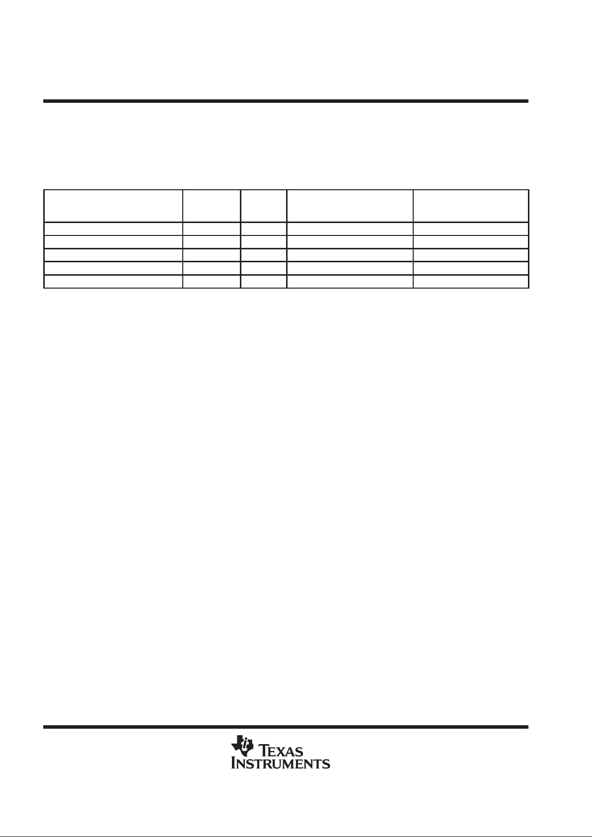
address matching
Connect status of the ASP is computed by a match of the address received in the last valid shadow protocol
against that at the address inputs (A9–A0) as well as against the three dedicated addresses that are internal
to the ASP (DSA, RSA, and TSA). The address map is shown in Table 2.
Table 2. Address Map
ADDRESS NAME
BINARY
CODE
HEX
CODE
SHADOW-PROTOCOL
RESULT
RESULTANT
PRIMARY-TO-SECONDARY
CONNECT STATUS
Reset Address (RSA) 0000000000 000 RESET RESET
Matching Address A9–A0 A9–A0 MATCH ON
Disconnect Address (DSA) 1111111110 3FE DISCONNECT OFF
Test Synchronization Address (TSA) 1111111111 3FF TEST SYNCHRONIZATION MULTICAST
All Other Addresses All others All others NO MATCH OFF
If the shadow-protocol address matches the address inputs (A9–A0), then the ASP responds by transmitting
an acknowledge protocol. Following the complete transmission of the acknowledge protocol, the ASP assumes
ON status (in which PTDI, PTDO, and PTMS are connected to STDO, STDI, and STMS, respectively). The ON
status allows the scan chain associated with the ASP’s secondary TAP to be controlled from the multidrop
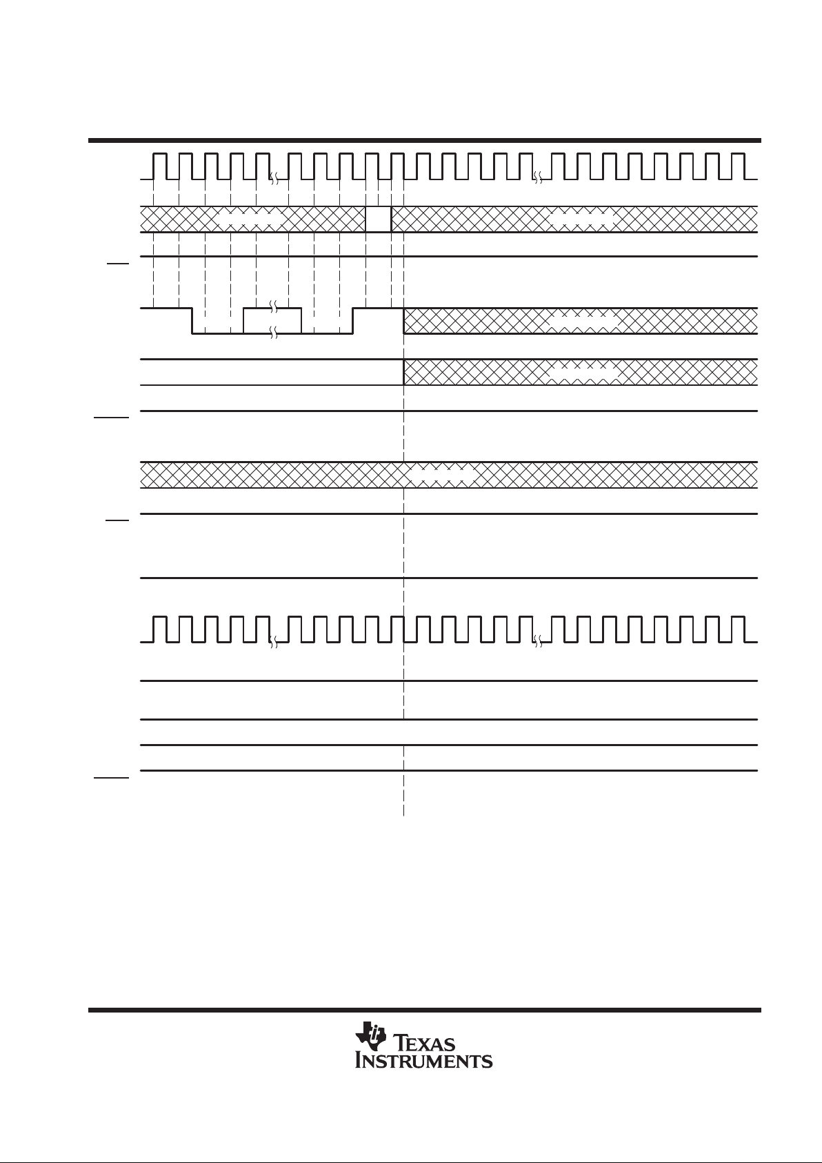
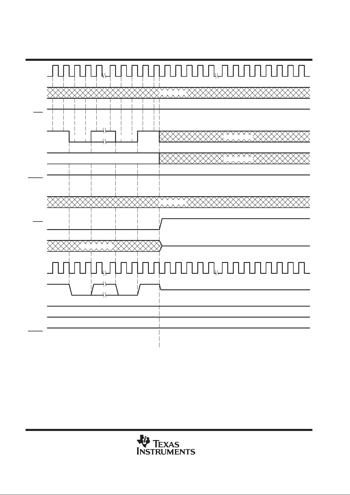
primary T AP as if it were directly wired as such. Figures 6 and 7 show the shadow-protocol timing for MATCH
result when the prior ASP connect status is ON and OFF, respectively.
If the shadow-protocol address does not match the address inputs (A9–A0), then (unless the address is one
of the three dedicated global addresses described below) the ASP responds immediately by assuming the OFF
status (in which PTDO and STDO are high impedance and STMS is held at its last level). This has the effect
of deselecting the scan chain associated with the ASP secondary T AP , but leaves the TAP state of the scan chain
unchanged. No acknowledge protocol is sent. Figures 8 and 9 show the shadow-protocol timing for NO MA TCH
result when the prior ASP connect status is ON and OFF, respectively.
disconnect address
The disconnect address (DSA) is one of the three internally dedicated addresses that are recognized globally .
When an ASP receives the DSA, it immediately responds by assuming the OFF status (in which PTDO and
STDO are high impedance and STMS is held at its last level). This has the effect of deselecting the scan chain
associated with the ASP secondary TAP, but leaves the TAP state of the scan chain unchanged. No
acknowledge protocol is sent. Figures 10 and 11 show the shadow-protocol timing for DISCONNECT result
when the prior ASP connect status is ON and OFF, respectively.
The same result occurs when a non-matching address is received. No specific action to disconnect an ASP is
required, as a given ASP is disconnected by the address that connects another. The dedicated DSA ensures
that at least one address is available for the purpose of disconnecting all receiving ASPs. It is especially useful
when the currently selected scan chain is in a different T AP state than that to be selected. In such a case, the
DSA is used to leave the former scan chain in the proper state, after which the primary T AP state is moved to
that needed to select the latter scan chain.
reset address
The reset address (RSA) is one of the three internally dedicated addresses that are recognized globally . When
an ASP receives the RSA, it immediately responds by assuming the RESET status (in which PTDO and STDO
are high impedance and STMS is forced to the high level). This has the effect of deselecting and resetting (to
Test-Logic-Reset state) the scan chain associated with the ASP secondary TAP. No acknowledge protocol is
sent. Figures 12 and 13 show the shadow-protocol timing for RESET result when the prior ASP connect status
is ON and OFF, respectively.

SN54ABT8996, SN74ABT8996
10-BIT ADDRESSABLE SCAN PORTS
MULTIDROP-ADDRESSABLE IEEE STD 1149.1 (JTAG) TAP TRANSCEIVERS
SCBS489C – AUGUST 1994 – REVISED APRIL 1999
13
POST OFFICE BOX 655303 • DALLAS, TEXAS 75265
test synchronization address
The test synchronization address (TSA) is one of the three internally dedicated addresses that are recognized
globally . When an ASP receives the TSA while its secondary TAP state is Pause-DR or Pause-IR, it immediately
responds by assuming the MUL TICAST status (in which PTDI and PTMS are connected to STDO and STMS
respectively , while PTDO is high impedance). No acknowledge protocol is sent. The TSA is valid only when the
T AP state of both primary and secondary is Pause-DR or Pause-IR. If the TSA is received when the TAP state
of either primary or secondary is Test-Logic-Reset or Run-Test-Idle, the shadow-protocol result is considered
to be DISCONNECT . Figures 14 and 15 show the shadow-protocol timing for TEST SYNCHRONIZA TION result
when the prior ASP connect status is ON and OFF, respectively.
The TSA allows simultaneous operation of the scan chains of all selected ASPs, either for global TAP-state
movement or for scan input of common serial test data via PTDI. This is especially useful in the former case,
to simultaneously move such scan chains into the Run-Test/Idle state in which module-level or
module-to-module BIST operations can operate synchronous to TCK in that TAP state, and in the later case,
to scan common test setup/data into multiple like modules.
protocol bypass
Protocol bypass is selected by a low BYP input. This protocol-bypass mode forces the ASP into BYP status
(primary T AP signals are connected to secondary TAP signals) regardless of previous shadow-protocol results.
The CON
output is made active (low). Receipt of shadow protocols is disabled.
When BYP
is taken low, the primary TAP serial data signals (PTDI, PTDO) are immediately (asynchronously
to PTCK) connected to their respective secondary T AP signals (STDO, STDI). The primary TAP mode-select
signal (PTMS) is also connected to its respective secondary T AP signal (STMS) unless PTRST
is low, in which
case STMS remains high until PTRST
is released. Also, the shadow-protocol-receive block is reset to its
power-up state and is held in this state such that select protocols appearing at the primary TAP are ignored.
When the BYP
input is released (taken high), the ASP immediately (asynchronously to PTCK) resumes the
connect status selected by the last valid shadow protocol. The shadow-protocol-receive block is again enabled
to respond to select protocols.
Figures 19 and 20 show protocol-bypass timing when the ASP connect status before BYP
active is ON and OFF ,
respectively .
asynchronous reset
While the PTRST input is always buffered directly to the STRST output, it also serves as an asynchronous reset
for the ASP . Given that BYP
is high, when PTRST goes low, the ASP immediately assumes TRST status in which
CON
is high and PTDO and STDO are at high impedance. Otherwise, if BYP is low, the ASP assumes
BYP/TRST status. In either case, STMS is set high so that connected IEEE Std 1 149.1-compliant devices can
be synchronously driven to their Test-Logic-Reset states. While PTRST
is low, receipt of shadow protocols
is disabled.
Figures 21 and 22 show asynchronous reset timing when the ASP connect status before PTRST
active is ON
and OFF, respectively. Figure 23 shows asynchronous reset timing when BYP
is low.
connect indicator
The CON output indicates secondary-scan-port activity (STDO, STMS active) regardless of whether such
activity is achieved via protocol bypass or shadow protocol. If the BYP
input is low, the CON output is low.
Otherwise, if the BYP
input is high, the CON output is low if the result of the last valid shadow protocol is MA TCH
or TEST SYNCHRONIZATION. In all other cases, and while acknowledge protocol is in progress, the CON
output is high.
SN54ABT8996, SN74ABT8996
10-BIT ADDRESSABLE SCAN PORTS
MULTIDROP-ADDRESSABLE IEEE STD 1149.1 (JTAG) TAP TRANSCEIVERS
SCBS489C – AUGUST 1994 – REVISED APRIL 1999
14
POST OFFICE BOX 655303 • DALLAS, TEXAS 75265
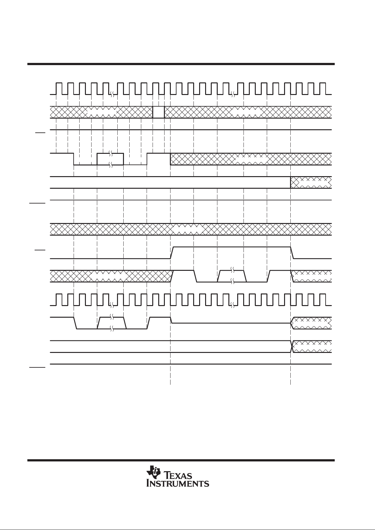
shadow-protocol timing
PTDI
PTDO
CON
STDO
STMS
A9–A0
Don’t Care
†
Don’t Care Don’t Care
A0PA9
P
A0PA9
P
PTDO = STDI
STMS = PTMS
A0PA9
P
STMS = STMS
0
PTCK
STCK
PTMS Don’t Care
STDI
STMS = PTMS
STDO = PTDI
PTDO = STDI
BYP
PTRST
STRST
Select Protocol Acknowledge Protocol ON
†
The instantaneous value of PTDI during protocol acknowledge is “don’t care” as long as the cumulative effect does not represent a protocol
hard-error or another valid select protocol.
Don’t Care
idle
select idle
idle select select idle
select
Figure 6. Shadow-Protocol Timing, Protocol Result = MATCH, Prior Connect Status = ON

SN54ABT8996, SN74ABT8996
10-BIT ADDRESSABLE SCAN PORTS
MULTIDROP-ADDRESSABLE IEEE STD 1149.1 (JTAG) TAP TRANSCEIVERS
SCBS489C – AUGUST 1994 – REVISED APRIL 1999
15
POST OFFICE BOX 655303 • DALLAS, TEXAS 75265
PTDI
PTDO
CON
STDO
STMS
A9–A0
Don’t Care
†
Don’t Care Don’t Care
A0PA9
P
A0PA9
P
STMS = STMS
0
PTCK
STCK
PTMS Don’t Care
STDI
STMS = PTMS
STDO = PTDI
PTDO = STDI
BYP
PTRST
STRST
Select Protocol Acknowledge Protocol ON
†
The instantaneous value of PTDI during protocol acknowledge is “don’t care” as long as the cumulative effect does not represent a protocol
hard-error or another valid select protocol.
Don’t Care
idle
select select idle
idle select select idle
Figure 7. Shadow-Protocol Timing, Protocol Result = MATCH, Prior Connect Status = OFF

SN54ABT8996, SN74ABT8996
10-BIT ADDRESSABLE SCAN PORTS
MULTIDROP-ADDRESSABLE IEEE STD 1149.1 (JTAG) TAP TRANSCEIVERS
SCBS489C – AUGUST 1994 – REVISED APRIL 1999
16
POST OFFICE BOX 655303 • DALLAS, TEXAS 75265
PTDI
PTDO
CON
STDO
STMS
A9–A0
Don’t Care
NMA
P
PTDO = STDI
STMS = PTMS
STMS = STMS
0
PTCK
STCK
PTMS
STDI
BYP
PTRST
STRST
Select Protocol OFF
Don’t Care
idle
select select idle
NMA
P
Don’t Care
Don’t Care Don’t Care
Figure 8. Shadow-Protocol Timing, Protocol Result = NO MATCH, Prior Connect Status = ON
SN54ABT8996, SN74ABT8996
10-BIT ADDRESSABLE SCAN PORTS
MULTIDROP-ADDRESSABLE IEEE STD 1149.1 (JTAG) TAP TRANSCEIVERS
SCBS489C – AUGUST 1994 – REVISED APRIL 1999
17
POST OFFICE BOX 655303 • DALLAS, TEXAS 75265
PTDI
PTDO
CON
STDO
STMS
A9–A0
Don’t Care
NMA
P
STMS = STMS
0
PTCK
STCK
PTMS
STDI
BYP
PTRST
STRST
Select Protocol OFF
Don’t Care
idle
select select idle
Don’t Care
Don’t Care Don’t Care
Figure 9. Shadow-Protocol Timing, Protocol Result = NO MATCH, Prior Connect Status = OFF
SN54ABT8996, SN74ABT8996
10-BIT ADDRESSABLE SCAN PORTS
MULTIDROP-ADDRESSABLE IEEE STD 1149.1 (JTAG) TAP TRANSCEIVERS
SCBS489C – AUGUST 1994 – REVISED APRIL 1999
18
POST OFFICE BOX 655303 • DALLAS, TEXAS 75265
PTDI
PTDO
CON
STDO
STMS
A9–A0
Don’t Care
DSA
P
PTDO = STDI
STMS = PTMS
STMS = STMS
0
PTCK
STCK
PTMS
STDI
BYP
PTRST
STRST
Select Protocol OFF
Don’t Care
idle
select select idle
DSA
P
Don’t Care
Don’t Care
Figure 10. Shadow-Protocol Timing, Protocol Result = DISCONNECT, Prior Connect Status = ON

SN54ABT8996, SN74ABT8996
10-BIT ADDRESSABLE SCAN PORTS
MULTIDROP-ADDRESSABLE IEEE STD 1149.1 (JTAG) TAP TRANSCEIVERS
SCBS489C – AUGUST 1994 – REVISED APRIL 1999
19
POST OFFICE BOX 655303 • DALLAS, TEXAS 75265
PTDI
PTDO
CON
STDO
STMS
A9–A0
Don’t Care
DSA
P
STMS = STMS
0
PTCK
STCK
PTMS
STDI
BYP
PTRST
STRST
Select Protocol OFF
Don’t Care
idle
select select idle
Don’t Care
Don’t Care
Figure 11. Shadow-Protocol Timing, Protocol Result = DISCONNECT, Prior Connect Status = OFF

SN54ABT8996, SN74ABT8996
10-BIT ADDRESSABLE SCAN PORTS
MULTIDROP-ADDRESSABLE IEEE STD 1149.1 (JTAG) TAP TRANSCEIVERS
SCBS489C – AUGUST 1994 – REVISED APRIL 1999
20
POST OFFICE BOX 655303 • DALLAS, TEXAS 75265
PTDI
PTDO
CON
STDO
STMS
A9–A0
Don’t Care
RSA
P
PTDO = STDI
STMS = PTMS
PTCK
STCK
PTMS
STDI
BYP
PTRST
STRST
Select Protocol RESET
Don’t Care
idle
select select idle
RSA
P
Don’t Care
Don’t Care
Figure 12. Shadow-Protocol Timing, Protocol Result = RESET, Prior Connect Status = ON

SN54ABT8996, SN74ABT8996
10-BIT ADDRESSABLE SCAN PORTS
MULTIDROP-ADDRESSABLE IEEE STD 1149.1 (JTAG) TAP TRANSCEIVERS
SCBS489C – AUGUST 1994 – REVISED APRIL 1999
21
POST OFFICE BOX 655303 • DALLAS, TEXAS 75265
PTDI
PTDO
CON
STDO
STMS
A9–A0
Don’t Care
RSA
P
STMS = STMS
0
PTCK
STCK
PTMS
STDI
BYP
PTRST
STRST
Select Protocol RESET
Don’t Care
idle
select select idle
Don’t Care
Don’t Care
Figure 13. Shadow-Protocol Timing, Protocol Result = RESET, Prior Connect Status = OFF

SN54ABT8996, SN74ABT8996
10-BIT ADDRESSABLE SCAN PORTS
MULTIDROP-ADDRESSABLE IEEE STD 1149.1 (JTAG) TAP TRANSCEIVERS
SCBS489C – AUGUST 1994 – REVISED APRIL 1999
22
POST OFFICE BOX 655303 • DALLAS, TEXAS 75265
PTDI
PTDO
CON
STDO
STMS
A9–A0
Don’t Care
TSA
P
STMS = PTMS
PTCK
STCK
PTMS
STDI
BYP
PTRST
STRST
Select Protocol MULTICAST
Don’t Care
idle
select select idle
Don’t Care
Don’t Care
STMS = PTMS
STDO = PTDI
PTDO = STDI
TSA
P
Figure 14. Shadow-Protocol Timing,
Protocol Result = TEST SYNCHRONIZATION, Prior Connect Status = ON

SN54ABT8996, SN74ABT8996
10-BIT ADDRESSABLE SCAN PORTS
MULTIDROP-ADDRESSABLE IEEE STD 1149.1 (JTAG) TAP TRANSCEIVERS
SCBS489C – AUGUST 1994 – REVISED APRIL 1999
23
POST OFFICE BOX 655303 • DALLAS, TEXAS 75265
PTDI
PTDO
CON
STDO
STMS
A9–A0
Don’t Care
TSA
P
PTCK
STCK
PTMS
STDI
BYP
PTRST
STRST
Select Protocol MULTICAST
Don’t Care
idle
select select idle
Don’t Care
Don’t Care
STMS = PTMS
STDO = PTDI
STMS = STMS
0
Figure 15. Shadow-Protocol Timing,
Protocol Result = TEST SYNCHRONIZATION, Prior Connect Status = OFF

SN54ABT8996, SN74ABT8996
10-BIT ADDRESSABLE SCAN PORTS
MULTIDROP-ADDRESSABLE IEEE STD 1149.1 (JTAG) TAP TRANSCEIVERS
SCBS489C – AUGUST 1994 – REVISED APRIL 1999
24
POST OFFICE BOX 655303 • DALLAS, TEXAS 75265
PTDI
PTDO
CON
STDO
STMS
A9–A0
Don’t Care
PTDO = STDI
STMS = PTMS
STMS = STMS
0
PTCK
STCK
PTMS
STDI
BYP
PTRST
STRST
Select Protocol
(aborted)
OFF
Don’t Care
idle
select select idleD0PDn
P
D0PDn
P
Don’t Care
Don’t Care
NOTE A: The position of PTMS shown in this figure is only one of many that would produce protocol result HARD ERROR.
Figure 16. Shadow-Protocol Timing,
Protocol Result = HARD ERROR (PTMS change during select protocol), Prior Connect Status = ON

SN54ABT8996, SN74ABT8996
10-BIT ADDRESSABLE SCAN PORTS
MULTIDROP-ADDRESSABLE IEEE STD 1149.1 (JTAG) TAP TRANSCEIVERS
SCBS489C – AUGUST 1994 – REVISED APRIL 1999
25
POST OFFICE BOX 655303 • DALLAS, TEXAS 75265
PTDI
PTDO
CON
STDO
STMS
A9–A0
Don’t Care
Don’t Care Don’t Care
A0PA9
P
PTDO = STDI
STMS = PTMS
A0PA9
P
STMS = STMS
0
PTCK
STCK
STDI
BYP
PTRST
STRST
Select Protocol Acknowledge Protocol
(aborted)
OFF
Don’t Care
idle
select select idle
PTMS
Don’t Care
NOTE A: The position of PTMS shown in this figure is only one of many that would produce protocol result HARD ERROR.
idle
Figure 17. Shadow-Protocol Timing,
Protocol Result = HARD ERROR (PTMS change during acknowledge protocol),
Prior Connect Status = ON

SN54ABT8996, SN74ABT8996
10-BIT ADDRESSABLE SCAN PORTS
MULTIDROP-ADDRESSABLE IEEE STD 1149.1 (JTAG) TAP TRANSCEIVERS
SCBS489C – AUGUST 1994 – REVISED APRIL 1999
26
POST OFFICE BOX 655303 • DALLAS, TEXAS 75265
PTDI
PTDO
CON
STDO
STMS
A9–A0
Don’t Care
STMS = PTMS
PTCK
STCK
PTMS
STDI
BYP
PTRST
STRST
Select Protocol
(aborted)
ON
Don’t Care
idle
select select idleselect
Don’t Care
Don’t Care
PTDO = STDI
STMS = PTMS
STDO = PTDI
NOTE A: The sequence of PTDI bits shown in this figure is only one of many that would produce protocol result SOFT ERROR.
Figure 18. Shadow-Protocol Timing,
Protocol Result = SOFT ERROR, Prior Connect Status = ON

SN54ABT8996, SN74ABT8996
10-BIT ADDRESSABLE SCAN PORTS
MULTIDROP-ADDRESSABLE IEEE STD 1149.1 (JTAG) TAP TRANSCEIVERS
SCBS489C – AUGUST 1994 – REVISED APRIL 1999
27
POST OFFICE BOX 655303 • DALLAS, TEXAS 75265
protocol-bypass timing
PTDI
PTDO
CON
STDO
STMS
A9–A0
PTCK
STCK
PTMS
STDI
BYP
PTRST
STRST
ON
Don’t Care
Don’t Care
Don’t Care
Don’t Care
ON BYP
STMS = PTMS
STDO = PTDI
PTDO = STDI
Figure 19. Protocol-Bypass Timing, Prior Connect Status = ON

SN54ABT8996, SN74ABT8996
10-BIT ADDRESSABLE SCAN PORTS
MULTIDROP-ADDRESSABLE IEEE STD 1149.1 (JTAG) TAP TRANSCEIVERS
SCBS489C – AUGUST 1994 – REVISED APRIL 1999
28
POST OFFICE BOX 655303 • DALLAS, TEXAS 75265
STMS = STMS
0
OFF
Don’t Care
STMS = STMS
0
Don’t Care
Don’t Care
Don’t Care
OFF BYP
STMS = PTMS
STDO = PTDI
PTDO = STDI
PTDI
PTDO
CON
STDO
STMS
A9–A0
PTCK
STCK
PTMS
STDI
BYP
PTRST
STRST
Figure 20. Protocol-Bypass Timing, Prior Connect Status = OFF

SN54ABT8996, SN74ABT8996
10-BIT ADDRESSABLE SCAN PORTS
MULTIDROP-ADDRESSABLE IEEE STD 1149.1 (JTAG) TAP TRANSCEIVERS
SCBS489C – AUGUST 1994 – REVISED APRIL 1999
29
POST OFFICE BOX 655303 • DALLAS, TEXAS 75265
asynchronous reset timing
PTDI
PTDO
CON
STDO
STMS
A9–A0
PTDO = STDI
PTCK
STCK
PTMS
STDI
BYP
PTRST
STRST
ON
Don’t Care
Don’t Care
Don’t Care
Don’t Care
STDO = PTDI
STMS = PTMS
TRST RESET
Figure 21. Asynchronous Reset Timing, Prior Connect Status = ON

SN54ABT8996, SN74ABT8996
10-BIT ADDRESSABLE SCAN PORTS
MULTIDROP-ADDRESSABLE IEEE STD 1149.1 (JTAG) TAP TRANSCEIVERS
SCBS489C – AUGUST 1994 – REVISED APRIL 1999
30
POST OFFICE BOX 655303 • DALLAS, TEXAS 75265
PTDI
PTDO
CON
STDO
STMS
A9–A0
PTCK
STCK
PTMS
STDI
BYP
PTRST
STRST
OFF
Don’t Care
Don’t Care
Don’t Care
Don’t Care
TRST
STMS = STMS
0
RESET
Figure 22. Asynchronous Reset Timing, Prior Connect Status = OFF

SN54ABT8996, SN74ABT8996
10-BIT ADDRESSABLE SCAN PORTS
MULTIDROP-ADDRESSABLE IEEE STD 1149.1 (JTAG) TAP TRANSCEIVERS
SCBS489C – AUGUST 1994 – REVISED APRIL 1999
31
POST OFFICE BOX 655303 • DALLAS, TEXAS 75265
PTDI
PTDO
CON
STDO
STMS
A9–A0
PTCK
STCK
PTMS
STDI
BYP
PTRST
STRST
BYP
Don’t Care
Don’t Care
Don’t Care
Don’t Care
BYP/TRST
STMS = PTMS
STMS = PTMS
BYP
PTDO = STDI
STDO = PTDI
Figure 23. Asynchronous Reset Timing, BYP = L

SN54ABT8996, SN74ABT8996
10-BIT ADDRESSABLE SCAN PORTS
MULTIDROP-ADDRESSABLE IEEE STD 1149.1 (JTAG) TAP TRANSCEIVERS
SCBS489C – AUGUST 1994 – REVISED APRIL 1999
32
POST OFFICE BOX 655303 • DALLAS, TEXAS 75265
absolute maximum ratings over operating free-air temperature range (unless otherwise noted)
†
Supply voltage range, V
CC
–0.5 V to 7 V. . . . . . . . . . . . . . . . . . . . . . . . . . . . . . . . . . . . . . . . . . . . . . . . . . . . . . . . . .
Input voltage range, V
I
(see Note 1) –0.5 V to 7 V. . . . . . . . . . . . . . . . . . . . . . . . . . . . . . . . . . . . . . . . . . . . . . . . . .
Voltage range applied to any output in the high state or power-off state, V
O
–0.5 V to 5.5 V. . . . . . . . . . . . . .
Current into any output in the low state, I
O
: SN54ABT8996 96 mA. . . . . . . . . . . . . . . . . . . . . . . . . . . . . . . . . . .
SN74ABT8996 128 mA. . . . . . . . . . . . . . . . . . . . . . . . . . . . . . . . . . .
Input clamp current, I
IK
(V
I
< 0) –18 mA. . . . . . . . . . . . . . . . . . . . . . . . . . . . . . . . . . . . . . . . . . . . . . . . . . . . . . . . . . .
Output clamp current, I
OK
(V
O
< 0) –50 mA. . . . . . . . . . . . . . . . . . . . . . . . . . . . . . . . . . . . . . . . . . . . . . . . . . . . . . . .
Package thermal impedance, θ
JA
(see Note 2):DW package 81°C/W. . . . . . . . . . . . . . . . . . . . . . . . . . . . . . . . .
PW package 120°C/W. . . . . . . . . . . . . . . . . . . . . . . . . . . . . . . .
Storage temperature range, T
stg
–65°C to 150°C. . . . . . . . . . . . . . . . . . . . . . . . . . . . . . . . . . . . . . . . . . . . . . . . . . .
†
Stresses beyond those listed under “absolute maximum ratings” may cause permanent damage to the device. These are stress ratings only, and
functional operation of the device at these or any other conditions beyond those indicated under “recommended operating conditions” is not
implied. Exposure to absolute-maximum-rated conditions for extended periods may affect device reliability.
NOTES: 1. The input and output negative-voltage ratings can be exceeded if the input and output clamp-current ratings are observed.
2. The package thermal impedance is calculated in accordance with JESD 51.
recommended operating conditions
SN54ABT8996 SN74ABT8996
MIN MAX MIN MAX
UNIT
V
CC
Supply voltage 4.5 5.5 4.5 5.5 V
V
IH
High-level input voltage 2 2 V
V
IL
Low-level input voltage 0.8 0.8 V
V
I
Input voltage 0 V
CC
0 V
CC
V
I
OH
High-level output current –24 –32 mA
I
OL
Low-level output current 48 64 mA
∆t/∆v Input transition rise or fall rate 10 10 ns/V
T
A
Operating free-air temperature –55 125 –40 85 °C

SN54ABT8996, SN74ABT8996
10-BIT ADDRESSABLE SCAN PORTS
MULTIDROP-ADDRESSABLE IEEE STD 1149.1 (JTAG) TAP TRANSCEIVERS
SCBS489C – AUGUST 1994 – REVISED APRIL 1999
33
POST OFFICE BOX 655303 • DALLAS, TEXAS 75265
electrical characteristics over recommended operating free-air temperature range (unless
otherwise noted)
TA = 25°C SN54ABT8996 SN74ABT8996
PARAMETER
TEST CONDITIONS
MIN TYP†MAX MIN MAX MIN MAX
UNIT
V
IK
VCC = 4.5 V, II = –18 mA –1.2 –1.2 –1.2 V
VCC = 4.5 V, IOH = –3 mA 2.5 2.5 2.5
VCC = 5 V, IOH = –3 mA 3 3 3
V
OH
IOH = –24 mA 2 2
V
V
CC
=
4.5 V
IOH = –32 mA 2* 2
IOL = 48 mA 0.55 0.55
V
OL
V
CC
= 4.5
V
IOL = 64 mA 0.55* 0.55
V
I
I
VCC = 0 to 5.5 V,
VI = VCC or GND
PTCK ±1 ±1 µA
PTDI, PTMS,
PTRST
10 10 10
IIHV
CC
= 5.5 V,
V
I
=
V
CC
A9–A0, BYP
,
STDI
10 10 10
µ
A
PTDI, PTMS,
PTRST
–13 –50 –13 –50 –13 –50
IILV
CC
= 5.5 V,
V
I
=
GND
A9–A0, BYP,
STDI
–38 –150 –38 –150 –38 –150
µ
A
I
OZH
VCC = 5.5 V, VO = 2.7 V PTDO, STDO 10 10 10 µA
I
OZL
VCC = 5.5 V, VO = 0.5 V PTDO, STDO –10 –10 –10 µA
I
off
VCC = 0, VI or VO ≤ 4.5 V ±100 ±100 µA
I
CEX
VCC = 5.5 V, VO = 5.5 V Outputs high 50 50 50 µA
I
O
‡
VCC = 5.5 V, VO = 2.5 V –50 –110 –200 –50 –200 –50 –200 mA
OFF, STCK = H, STMS = H 0.8 1.5 1.5 1.5
VCC = 5.5 V,
ON, PTDO = L, STCK = L,
STDO = L, STMS = L
13 18 18 18
I
CC
I
O
= 0,
VI = VCC or GND
ON, PTDO = H, STCK = H,
STDO = H, STMS = H
3.2 5 5 5
mA
TRST, STCK = L 6 8 8 8
V
= 5.5 V , One input at 3.4 V,
∆I
CC
§
CC
,,
Other inputs at VCC or GND
1.5
1.5
1.5
mA
C
i
VI = 2.5 V or 0.5 V 5 pF
C
o
VO = 2.5 V or 0.5 V 8 pF
* On products compliant to MIL-PRF-38535, this parameter does not apply.
†
All typical values are at VCC = 5 V.
‡
Not more than one output should be tested at a time, and the duration of the test should not exceed one second.
§
This is the increase in supply current for each input that is at the specified TTL voltage level rather than VCC or GND.

SN54ABT8996, SN74ABT8996
10-BIT ADDRESSABLE SCAN PORTS
MULTIDROP-ADDRESSABLE IEEE STD 1149.1 (JTAG) TAP TRANSCEIVERS
SCBS489C – AUGUST 1994 – REVISED APRIL 1999
34
POST OFFICE BOX 655303 • DALLAS, TEXAS 75265
timing requirements over recommended ranges of supply voltage and operating free-air
temperature (unless otherwise noted) (see Figure 24)
SN54ABT8996 SN74ABT8996
MIN MAX MIN MAX
UNIT
f
clock
Clock frequency PTCK 0 40 0 40 MHz
BYP low
†
4.9 4.9
PTCK high 12 12
twPulse duration
PTCK low 6.5 6.5
ns
PTRST low 2.6 2.6
A9–A0 before PTCK↓
‡
6.6 6.6
p
PTDI before PTCK↑ 4.9 4.9
tsuSetup time
PTMS before BYP↑
†
0.8 0.6
ns
PTMS before PTCK↑ 9 9
A9–A0 after PTCK↓
‡
0.3 0.3
PTDI after PTCK↑ 0.7 0.7
thHold time
PTMS after BYP↑
†
2.4 2.4
ns
PTMS after PTCK↑ 1.3 1.3
†
In normal application of the ASP, such timing requirements with respect to BYP are met implicitly and, therefore, need not be considered.
‡
These requirements apply only in the case where the address inputs are changed during a shadow protocol. For normal application of the ASP,
it is recommended that the address inputs remain static throughout any shadow protocols. In such cases, the timing of address inputs relative
to PTCK need not be considered.

SN54ABT8996, SN74ABT8996
10-BIT ADDRESSABLE SCAN PORTS
MULTIDROP-ADDRESSABLE IEEE STD 1149.1 (JTAG) TAP TRANSCEIVERS
SCBS489C – AUGUST 1994 – REVISED APRIL 1999
35
POST OFFICE BOX 655303 • DALLAS, TEXAS 75265
switching characteristics over recommended ranges of supply voltage and operating free-air
temperature (unless otherwise noted) (see Figure 24)
SN54ABT8996
PARAMETER
FROM
(INPUT)
TO
(OUTPUT)
VCC = 5 V,
TA = 25°C
MIN MAX
UNIT
MIN TYP MAX
f
max
PTCK 40 40 MHz
t
PLH
BYP↑
1 3 4.2 1 5.3
t
PHL
BYP↓
CON
1 3.8 5.2 1 6.3
ns
t
PLH
2.5 7.8 10 2.5 12.9
t
PHL
BYP↓
STMS
2.5 5.2 7 2.5 8.9
ns
t
PLH
1 2.2 3.1 1 3.7
t
PHL
PTCK
STCK
1 2.8 3.9 1 4.6
ns
t
PLH
3.5 6.9 8.9 3.5 11.2
t
PHL
PTCK↓
CON
3.5 7 9.3 3.5 11.6
ns
t
PLH
PTCK
↓
p
3 7.6 9.9 3 12.6
t
PHL
(shad
ow-protoco
l
acknowledge)
PTDO
3 6.2 9.4 3 10.9
ns
t
PLH
†
PTCK
↓
5.5 12.1 15.4 5.5 19.9
t
PHL
†
(connect)
STMS
5.5 9.7 12.5 5.5 15.8
ns
t
PLH
1 3.1 4.4 1 5.4
t
PHL
PTDI
STDO
1 3.3 4.5 1 5.6
ns
t
PLH
1 3.2 4.4 1 5.5
t
PHL
PTMS
STMS
1 3.4 4.7 1 5.7
ns
t
PLH
1 3.2 4.8 1 5.8
t
PHL
PTRST
STRST
1 3.3 4.7 1 5.7
ns
CON 3.5 7.4 9.5 3.5 12.1
t
PLH
PTRST↓
STMS 2.5 5.6 7.7 2.5 9.6
ns
t
PLH
1 2.8 4 1 4.9
t
PHL
STDI
PTDO
1 3.3 4.6 1 5.7
ns
†
The transitions at STMS are possible only when a shadow-protocol select is issued while STMS is held (in the OFF status) at a level that differs
from that at PTMS. Such operation is not recommended since state synchronization of the primary TAP to secondary TAP cannot be ensured.

SN54ABT8996, SN74ABT8996
10-BIT ADDRESSABLE SCAN PORTS
MULTIDROP-ADDRESSABLE IEEE STD 1149.1 (JTAG) TAP TRANSCEIVERS
SCBS489C – AUGUST 1994 – REVISED APRIL 1999
36
POST OFFICE BOX 655303 • DALLAS, TEXAS 75265
switching characteristics over recommended ranges of supply voltage and operating free-air
temperature (unless otherwise noted) (continued) (see Figure 24)
SN54ABT8996
PARAMETER
FROM
(INPUT)
TO
(OUTPUT)
VCC = 5 V,
TA = 25°C
MIN MAX
UNIT
MIN TYP MAX
t
PZH
†
1.5 4 5.5 1.5 6.9
t
PZL
BYP↓
PTDO
1.5 4.5 6.1 1.5 7.5
ns
t
PZH
‡
1.5 3.7 5.2 1.5 6.2
t
PZL
BYP↓
STDO
1.5 4.2 5.8 1.5 6.9
ns
t
PZH
†
PTCK↓
PTDO 4 7.2 9.5 4 12.1 ns
t
PZH
‡
4 7.6 10 4 12.5
t
PZL
PTCK↓
STDO
4 8.1 10.7 4 12.8
ns
t
PHZ
†
1.5 3.6 4.8 1.5 5.5
t
PLZ
BYP↑
PTDO
1.3 3.6 4.9 1.3 5.8
ns
t
PHZ
‡
1.5 3.6 4.8 1.5 5.5
t
PLZ
BYP↑
STDO
1.5 3 4.2 1.5 4.8
ns
t
PHZ
†
3 6.2 8.2 3 11
t
PLZ
PTCK↓
PTDO
1 6.9 9.5 1 13.1
ns
t
PHZ
‡
3.5 7.3 9.2 3.5 12
t
PLZ
§
PTCK↓
STDO
1 7.1 8.7 1 10.4
ns
t
PHZ
†
3.5 6.6 9.2 3.5 11
t
PLZ
PTRST↓
PTDO
1 7.4 10.2 1 13.4
ns
t
PHZ
‡
4.5 9.4 12 4.5 13.6
t
PLZ
PTRST↓
STDO
3 7.3 9 3 10.5
ns
†
In most applications, the node to which PTDO is connected has a pullup resistor. In such cases, this parameter is not significant.
‡
In most applications, the node to which STDO is connected has a pullup resistor. In such cases, this parameter is not significant.
§
This parameter applies only in case of protocol hard error.

SN54ABT8996, SN74ABT8996
10-BIT ADDRESSABLE SCAN PORTS
MULTIDROP-ADDRESSABLE IEEE STD 1149.1 (JTAG) TAP TRANSCEIVERS
SCBS489C – AUGUST 1994 – REVISED APRIL 1999
37
POST OFFICE BOX 655303 • DALLAS, TEXAS 75265
switching characteristics over recommended ranges of supply voltage and operating free-air
temperature (unless otherwise noted) (see Figure 24)
SN74ABT8996
PARAMETER
FROM
(INPUT)
TO
(OUTPUT)
VCC = 5 V,
TA = 25°C
MIN MAX
UNIT
MIN TYP MAX
f
max
PTCK 40 40 MHz
t
PLH
BYP↑
1 3 4.2 1 4.8
t
PHL
BYP↓
CON
1 3.8 5.2 1 6
ns
t
PLH
2.5 7.8 10 2.5 12.2
t
PHL
BYP↓
STMS
2.5 5.2 7 2.5 8.4
ns
t
PLH
1 2.2 3.1 1 3.4
t
PHL
PTCK
STCK
1 2.8 3.9 1 4.5
ns
t
PLH
3.5 6.9 8.9 3.5 10.6
t
PHL
PTCK↓
CON
3.5 7 9.3 3.5 10.8
ns
t
PLH
PTCK
↓
p
3 7.6 9.9 3 11.8
t
PHL
(shad
ow-protoco
l
acknowledge)
PTDO
3 6.2 9.4 3 10.2
ns
t
PLH
†
PTCK
↓
5.5 12.1 15.4 5.5 18.6
t
PHL
†
(connect)
STMS
5.5 9.7 12.5 5.5 14.9
ns
t
PLH
1 3.1 4.4 1 5
t
PHL
PTDI
STDO
1 3.3 4.5 1 5.3
ns
t
PLH
1 3.2 4.4 1 5.1
t
PHL
PTMS
STMS
1 3.4 4.7 1 5.5
ns
t
PLH
1 3.2 4.8 1 5.7
t
PHL
PTRST
STRST
1 3.3 4.7 1 5.7
ns
CON 3.5 7.4 9.5 3.5 11.4
t
PLH
PTRST↓
STMS 2.5 5.6 7.7 2.5 9.2
ns
t
PLH
1 2.8 4 1 4.5
t
PHL
STDI
PTDO
1 3.3 4.6 1 5.4
ns
†
The transitions at STMS are possible only when a shadow-protocol select is issued while STMS is held (in the OFF status) at a level that differs
from that at PTMS. Such operation is not recommended since state synchronization of the primary TAP to secondary TAP cannot be ensured.

SN54ABT8996, SN74ABT8996
10-BIT ADDRESSABLE SCAN PORTS
MULTIDROP-ADDRESSABLE IEEE STD 1149.1 (JTAG) TAP TRANSCEIVERS
SCBS489C – AUGUST 1994 – REVISED APRIL 1999
38
POST OFFICE BOX 655303 • DALLAS, TEXAS 75265
switching characteristics over recommended ranges of supply voltage and operating free-air
temperature (unless otherwise noted) (continued) (see Figure 24)
SN74ABT8996
PARAMETER
FROM
(INPUT)
TO
(OUTPUT)
VCC = 5 V,
TA = 25°C
MIN MAX
UNIT
MIN TYP MAX
t
PZH
†
1.5 4 5.5 1.5 6.6
t
PZL
BYP↓
PTDO
1.5 4.5 6.1 1.5 7.2
ns
t
PZH
‡
1.5 3.7 5.2 1.5 6
t
PZL
BYP↓
STDO
1.5 4.2 5.8 1.5 6.7
ns
t
PZH
†
PTCK↓
PTDO 4 7.2 9.5 4 11.3 ns
t
PZH
‡
4 7.6 10 4 11.7
t
PZL
PTCK↓
STDO
4 8.1 10.7 4 12.2
ns
t
PHZ
†
1.5 3.6 4.8 1.5 5.3
t
PLZ
BYP↑
PTDO
1.5 3.6 4.9 1.5 5.3
ns
t
PHZ
‡
1.5 3.6 4.8 1.5 5.4
t
PLZ
BYP↑
STDO
1.5 3 4.2 1.5 4.4
ns
t
PHZ
†
3 6.2 8 3 10.3
t
PLZ
PTCK↓
PTDO
3 6.9 9.5 3 11.2
ns
t
PHZ
‡
3.5 7.3 9 3.5 10.9
t
PLZ
§
PTCK↓
STDO
3.5 7.1 8.7 3.5 10.4
ns
t
PHZ
†
3.5 6.6 8.5 3.5 10.4
t
PLZ
PTRST↓
PTDO
3.5 7.4 10.2 3.5 11.7
ns
t
PHZ
‡
4.5 9.4 11.5 4.5 13.2
t
PLZ
PTRST↓
STDO
4.5 7.3 9 4.5 10.5
ns
†
In most applications, the node to which PTDO is connected has a pullup resistor. In such cases, this parameter is not significant.
‡
In most applications, the node to which STDO is connected has a pullup resistor. In such cases, this parameter is not significant.
§
This parameter applies only in case of protocol hard error.

SN54ABT8996, SN74ABT8996
10-BIT ADDRESSABLE SCAN PORTS
MULTIDROP-ADDRESSABLE IEEE STD 1149.1 (JTAG) TAP TRANSCEIVERS
SCBS489C – AUGUST 1994 – REVISED APRIL 1999
39
POST OFFICE BOX 655303 • DALLAS, TEXAS 75265
PARAMETER MEASUREMENT INFORMATION
Output
Control
1.5 V
t
h
t
su
From Output
Under Test
CL = 50 pF
LOAD CIRCUIT
S1
7 V
Open
GND
500 Ω
500 Ω
Data Input
Timing Input
1.5 V
3 V
0 V
1.5 V 1.5 V
3 V
0 V
3 V
0 V
1.5 V 1.5 V
t
w
Input
(see Note A)
VOLTAGE WAVEFORMS
SETUP AND HOLD TIMES
VOLTAGE WAVEFORMS
PROPAGATION DELAY TIMES
INVERTING AND NONINVERTING OUTPUTS
VOLTAGE WAVEFORMS
PULSE DURATION
t
PLH
t
PHL
t
PHL
t
PLH
V
OH
V
OH
V
OL
V
OL
1.5 V 1.5 V
3 V
0 V
1.5 V1.5 V
Input
1.5 V
Output
Waveform 1
S1 at 7 V
(see Note B)
Output
Waveform 2
S1 at Open
(see Note B)
V
OL
V
OH
t
PZL
t
PZH
t
PLZ
t
PHZ
1.5 V1.5 V
3.5 V
0 V
1.5 V
VOL + 0.3 V
1.5 V
VOH – 0.3 V
[
0 V
3 V
VOLTAGE WAVEFORMS
ENABLE AND DISABLE TIMES
LOW- AND HIGH-LEVEL ENABLING
Output
Output
t
PLH/tPHL
t
PLZ/tPZL
t
PHZ/tPZH
Open
7 V
Open
TEST S1
NOTES: A. CL includes probe and jig capacitance.
B. Waveform 1 is for an output with internal conditions such that the output is low except when disabled by the output control.
Waveform 2 is for an output with internal conditions such that the output is high except when disabled by the output control.
C. All input pulses are supplied by generators having the following characteristics: PRR ≤ 10 MHz, ZO = 50 Ω, tr ≤ 2.5 ns, tf≤ 2.5 ns.
D. The outputs are measured one at a time with one transition per measurement.
Figure 24. Load Circuit and Voltage Waveforms

IMPORTANT NOTICE
T exas Instruments and its subsidiaries (TI) reserve the right to make changes to their products or to discontinue
any product or service without notice, and advise customers to obtain the latest version of relevant information
to verify, before placing orders, that information being relied on is current and complete. All products are sold
subject to the terms and conditions of sale supplied at the time of order acknowledgement, including those
pertaining to warranty, patent infringement, and limitation of liability.
TI warrants performance of its semiconductor products to the specifications applicable at the time of sale in
accordance with TI’s standard warranty. Testing and other quality control techniques are utilized to the extent
TI deems necessary to support this warranty. Specific testing of all parameters of each device is not necessarily
performed, except those mandated by government requirements.
CERT AIN APPLICATIONS USING SEMICONDUCTOR PRODUCTS MA Y INVOLVE POTENTIAL RISKS OF
DEATH, PERSONAL INJURY, OR SEVERE PROPERTY OR ENVIRONMENTAL DAMAGE (“CRITICAL
APPLICATIONS”). TI SEMICONDUCTOR PRODUCTS ARE NOT DESIGNED, AUTHORIZED, OR
WARRANTED TO BE SUITABLE FOR USE IN LIFE-SUPPORT DEVICES OR SYSTEMS OR OTHER
CRITICAL APPLICATIONS. INCLUSION OF TI PRODUCTS IN SUCH APPLICA TIONS IS UNDERST OOD TO
BE FULLY AT THE CUSTOMER’S RISK.
In order to minimize risks associated with the customer’s applications, adequate design and operating
safeguards must be provided by the customer to minimize inherent or procedural hazards.
TI assumes no liability for applications assistance or customer product design. TI does not warrant or represent
that any license, either express or implied, is granted under any patent right, copyright, mask work right, or other
intellectual property right of TI covering or relating to any combination, machine, or process in which such
semiconductor products or services might be or are used. TI’s publication of information regarding any third
party’s products or services does not constitute TI’s approval, warranty or endorsement thereof.
Copyright 1999, Texas Instruments Incorporated
 Loading...