

SN28837
1/2-INCH PAL TIMER
SOCS031B – JULY 1991
Copyright 1991, Texas Instruments Incorporated
1
POST OFFICE BOX 655303 • DALLAS, TEXAS 75265
• PAL-Timing Operation
• Solid-State Reliability
• Color and Monochrome Operation
• Five Selectable-Antiblooming Modes
• Variable-Integration-Time Option
• Surface-Mount Package
• Clamp-Pulse Select Option
• Horizontal and Vertical Resets for External
Synchronization
description
The SN28837 is a monolithic integrated circuit
designed to supply timing signals for the Texas
Instruments (TI) 8-mm-diagonal TC276 (PAL
color) and TC277 (P AL monochrome) CCD image
sensors. The SN28837 supplies both CCD-drive
signals and PAL-television synchronization
signals at standard video rates. It requires a
single 5-V supply voltage and a 13.37-MHz
crystal-oscillator input. The SN28837 provides the
user with several options including multiple
antiblooming modes, variable-integration time,
external synchronization, clamp-pulse selection,
and delayed horizontal transfer.
The SN28837 is designed to drive the CCD image sensor through intermediary level-shifting devices such as
the TI TMS3473B parallel driver and the SN28846 serial driver. It also supplies sample-and-hold signals for the
TI TL1593 3-channel sample-and-hold circuit and multiplex signals for the TI TL1051 video preprocessor. In
color applications, the SN28837 interfaces with the SN28838 color-subcarrier generator to generate the PAL
color subcarrier.
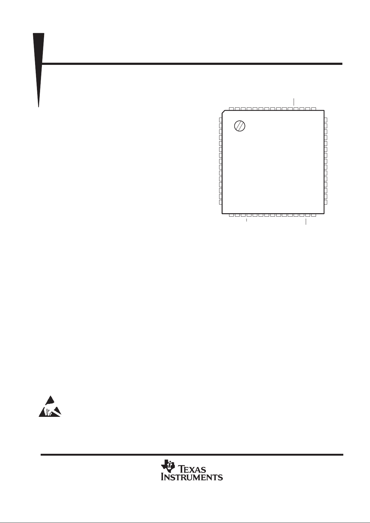
The SN28837 is supplied in a 60-pin plastic flat package and is characterized for operation from –20°C to 45°C.
This device contains circuits to protect its inputs and outputs against damage due to high static voltages or electrostatic fields. These
circuits have been qualified to protect this device against electrostatic discharges (ESD) of up to 2 kV according to MIL-STD-883C,
Method 3015; however, precautions should be taken to avoid application of any voltage higher than maximum-rated voltages to these
high-impedance circuits. During storage or handling, the device leads should be shorted together or the device should be placed in
conductive foam. In a circuit, unused inputs should always be connected to an appropriate logic voltage level, preferably either VCC or ground.
Specific guidelines for handling devices of this type are contained in the publication
Guidelines for Handling Electrostatic-Discharge-Sensitive
(ESDS) Devices and Assemblies
available from Texas Instruments.
TI is a trademark of Texas Instruments Incorporated.
V
CC
V
CC1
X2
X1
GND
V
CC
PI
ABIN
GT
PS
NC
S3
S2
S1
T
1
2
3
4
5
6
7
8
9
10
11
12
13
14
15
45
44
43
42
41
40
39
38
37
36
35
34
33
32
31
BCP1
BCP2
CP1
CP2
CSYNC
CBLK
BF
VD
SCBLK
IDP
HGATE
TESTA
FI
SFI
NC
17 18 19 20 21 22 23 24 25 26 27 28 29
59 58 57 56 55 5453 525150 4948 47
HCR
VCR
GT2
SH1
CLK
PD
LSW
CLK13M
NC
GT3/SH2
NC
NC
GT1/SH3
16 30
NC
46
GND
60
TESTC
VDS
HIGH
GPS
GP
VD2
ABS1
ABS2
ABS0
VGATE
NC
TESTB
E/L
V
CC
SB
FS PACKAGE
(TOP VIEW)
NC – No internal connection
PRODUCTION DATA information is current as of publication date.
Products conform to specifications per the terms of Texas Instruments
standard warranty. Production processing does not necessarily include
testing of all parameters.
SN28837
1/2-INCH PAL TIMER
SOCS031B – JULY 1991
2
POST OFFICE BOX 655303 • DALLAS, TEXAS 75265
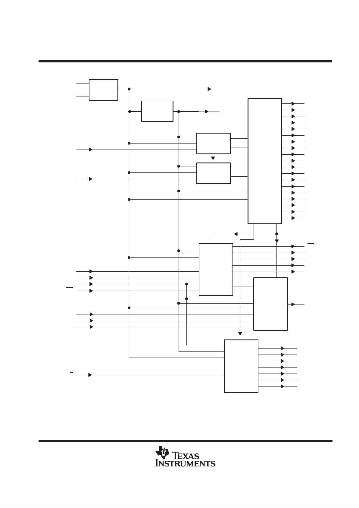
functional block diagram
Oscillator
Divide
by 4
13 MHz
3.3 MHz
Horizontal
Counter
Vertical
Counter
Clock
Generator
Antiblooming
Generator
Serial
Generator
Decoder
49
37
39
36
31
PD
GT
PI
PS
T
S1
S2
S3
SH1
GT3/SH2
GT1/SH3
GT2
32
33
34
51
53
56
57
38
ABIN
GPS
GP
VDS
SB
ABS0
ABS1
ABS2
21
22
23
E/L
19
HCR
59
VCR
58
X1
42
X2
43
50
CLK
47
CLK13M
26
27
18
29
1
2
3
4
5
6
7
8
48
9
10
12
16
17
28
20
11
12
14
BCP1
BCP2
CP1
CP2
CSYNC
CBLK
BF
VD
LSW
SCBLK
IDP
TESTA
TESTB
TESTC
VD2
VGATE
HGATE
FI
SFI
The levels on these three terminals determine which of the five antiblooming modes is selected:
Mode
ABS2 ABS1 ABS0 Operation
0 NC L L No ABG pulses
1 NC H L 2-MHz burst of ABG pulses
2 NC L H 1-MHz burst of ABG pulses
3 H H H 1-MHz continuous ABG pulses
4 L H H 2-MHz continuous ABG pulses
SN28837
1/2-INCH PAL TIMER
SOCS031B – JULY 1991
3
POST OFFICE BOX 655303 • DALLAS, TEXAS 75265
Terminal Functions
TERMINAL
NAME NO.
I/O
DESCRIPTION
ABIN 38 O Antiblooming in
ABS0 21 I
ABS1 22 I
ABS2 23 I
Mode 1 is used for normal operation.
BCP1 1 O Optical black clamp
BCP2 2 O Optical black clamp
BF 7 O Burst flag
CBLK 6 O Composite blank
CLK 50 O 3.34-MHz clock (factory-test point)
CLK13M 47 O 13-MHz clock (connect to SN28838 color-subcarrier generator for color operation)
CP1 3 O Clamp 1 (signal processing)
CP2 4 O Clamp 2 (signal processing)
CSYNC 5 O Composite sync
E/L 19 I
Delay select for S1, S2, S3. When E/L is high, the three serial-transfer pulses occur early relative to the
sample-and-hold pulses SH1, SH2, and SH3. When E/L
is low, the three serial-transfer pulses occur late
relative to the sample-and-hold pulses.
FI 13 O Field index
GND 41, 60 Ground
GP 27 I Exposure control: GP gates the PS and PI outputs (see the description of GPS)
GPS 26 I
When GPS is high, the timer operates in the normal-integration-time mode (t
int
= 20 ms) and VD is
connected internally to GP. To operate the imager in the variable-integration-time mode, GPS must be
held low and a user-defined logic circuit must be inserted between VD and GP to vary the integration time
(see Figure 1).
GT 37 O TMS3473B parallel-driver MIDSEL input switch
GT1/SH3 56 O
GT1/SH3 is a logic signal for both Y gate 1 of the TL1051 video preprocessor and sample-and-hold
channel 3 of the TL1593 3-channel sample-and-hold circuit.
GT2 57 O Y gate 2 for the TL1051 video preprocessor
GT3/SH2 53 O
GT3/SH2 is a logic signal for both Y gate 3 of the TL1051 video preprocessor and sample-and-hold
channel 2 of the TL1593 3-channel sample-and-hold circuit.
HCR 59 I Horizontal-counter reset
HGATE 11 O Decoded H count signal. HGATE is a test point and is not used in normal operation.
HIGH 25 I Not used (tie high)
IDP 10 O ID pulse (for SECAM operation)
LSW 48 O Line switch (connect to SN28838 for color operation)
NC
15, 30,
35, 46,
52, 54, 55
No connect
PD 49 O Power down. A low-logic level on PD causes the device to enter a low power-consumption mode.
PI 39 O Parallel-image-area gate clock
PS 36 O Parallel-storage-area gate clock
SB 29 I
Standby-mode select. When SB is high, normal operation is selected; when SB is low, the power-down
mode is selected.
SCBLK 9 O Subcarrier blank (for SECAM applications)
SN28837
1/2-INCH PAL TIMER
SOCS031B – JULY 1991
4
POST OFFICE BOX 655303 • DALLAS, TEXAS 75265
Terminal Functions (Continued)
TERMINAL
NAME NO.
I/O
DESCRIPTION
SFI 14 O Second field index
SH1 51 O Sample and hold 1
S1 32 O Serial clock 1
S2 33 O Serial clock 2
S3 34 O Serial clock 3
T 31 O Transfer-gate clock
TESTA 12 O Test A (factory-test point)
TESTB 16 O Test B (factory-test point)
TESTC 17 O Test C (factory-test point)
V
CC
24, 40, 45 DC power
VCC1 44 Oscillator power
VCR 58 I Vertical-counter reset
VD 8 O Vertical drive
VDS 18 I
Vertical-dump speed. When VDS is high, the vertical-dump frequency is 3.3MHz; when VDS is low, the
vertical-dump frequency is 2 MHz.
VD2 28 O Real-display-area signal. VD2 is a test point and is not used in normal operation.
VGATE 20 O Decoded V count signal. VGATE is a test point and is not used in normal operation.
X1 42
X2 43
Crystal oscillator (see Figure 2)
12 3
t
int
Flush Pulses Transfer Pulse
GP
Figure 1. GP Flush and Transfer Pulses
SN28837
1/2-INCH PAL TIMER
SOCS031B – JULY 1991
5
POST OFFICE BOX 655303 • DALLAS, TEXAS 75265
variable-integration-time mode
In addition to the normal TV mode of operation, the SN28837 timing generator offers an optional
variable-integration mode for use with the TC276 and TC277 CCD area-array image sensors. The
variable-integration mode is selected by applying a low-logic level to GPS. This low-logic level disables the
vertical-drive (VD) signal from controlling, internal to the timer, the image-area and storage-area parallel transfer
signal (GP).
Prior to the start of a new integration period, the charge that has accumulated in the image area must be
transferred out. To flush this previous signal or dark-current charge from the image area, GP is pulsed low two
times. Each low pulse generates 302 pulses image-area and storage-area gate and transfer signals that shift
the unwanted charge into the clearing drain. This clearing function should be performed during the high time
of the VD signal (see Figure 3 through Figure 13).
The new integration period continues as long as GP remains high. GPS must be held at a low-logic level to
prevent VD from controlling GP internally . The integration ceases and the readout occurs when VD and GP are
pulsed low simultaneously; this is accomplished by taking GPS to a high-logic level. The readout timing is
dependent on the vertical-drive pulse; this means that the total-integration time is a multiple of 1/50 of a second
plus the time interval between the last GP low pulse and the next VD low pulse. The image readout occurs within
the normal 1/50-second readout interval. If the integration time is less than 1/50 of a second, normal output
operation occurs; if the integration time is greater than 1/50 of a second, a frame buffer may be required to
capture the image.
Integration times greater than 1/50 of a second result in image degradation at temperatures greater than 25°C
due to dark-current generation. The degradation is seen as a decrease in dynamic range (contrast) and an
increase in noise. It is recommended that the image sensor be cooled for long-exposure operation. The
dark-current generation is reduced by a factor of two for each 7°C temperature decrease. The sensor operates
at –30°C. Cooling can be accomplished by using a thermoelectric or Peltier cooler attached to the image sensor .
Condensation on the header must be prevented by isolating the cooled sensor from moist air. V acuum isolation
is preferred; however, the continual flushing of dry nitrogen across the header can also prevent condensation.
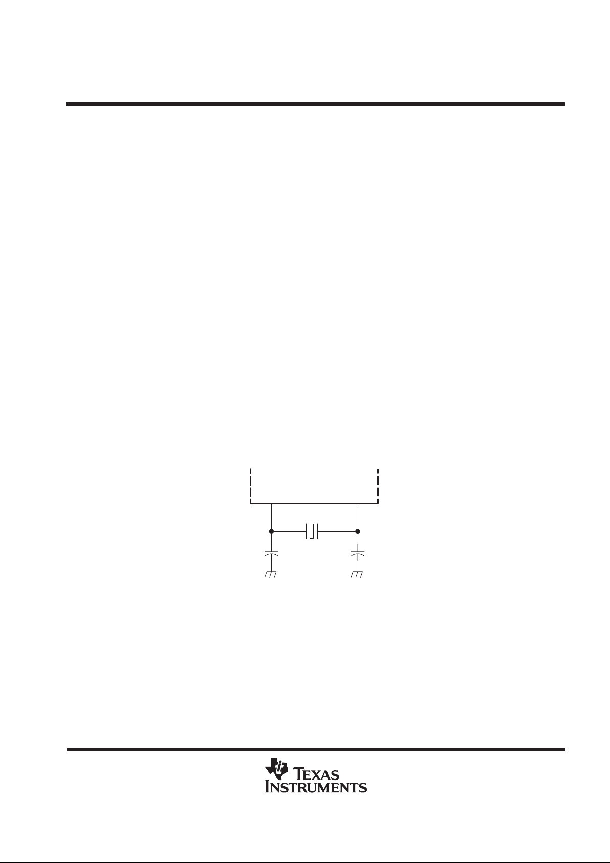
X1 X2
42 43
C1 ≈ 40 pF C2 ≈ 40 pF
SN28837
NOTE: The SN28837 is designed for use with a
crystal oscillator. The X1 and X2
terminals should not connect directly to
external driver outputs.
Figure 2. Connection of an External Crystal Oscillator to the SN28837
SN28837
1/2-INCH PAL TIMER
SOCS031B – JULY 1991
6
POST OFFICE BOX 655303 • DALLAS, TEXAS 75265
absolute maximum ratings over operating free-air temperature range (unless otherwise noted)
†
Supply voltage range, V
DD
(see Note 1) –0.3 V to 7 V. . . . . . . . . . . . . . . . . . . . . . . . . . . . . . . . . . . . . . . . . . . . . .
Input voltage range, V
I
–0.3 V to VDD + 0.3 V. . . . . . . . . . . . . . . . . . . . . . . . . . . . . . . . . . . . . . . . . . . . . . . . . . . . . .
Output voltage range, V
O
–0.3 V to VDD + 0.3 V. . . . . . . . . . . . . . . . . . . . . . . . . . . . . . . . . . . . . . . . . . . . . . . . . . .
Continuous total power dissipation at (or below) T
A
= 25°C 300 mW. . . . . . . . . . . . . . . . . . . . . . . . . . . . . . . . . .
Operating free-air temperature range, T
A
–20°C to 45°C. . . . . . . . . . . . . . . . . . . . . . . . . . . . . . . . . . . . . . . . . . . .
Storage temperature range, T
STG
–55°C to 125°C. . . . . . . . . . . . . . . . . . . . . . . . . . . . . . . . . . . . . . . . . . . . . . . . .
Lead temperature 1,6 mm (1/16 in) from case for 10 seconds 260°C. . . . . . . . . . . . . . . . . . . . . . . . . . . . . . . . . .
†
Stresses beyond those listed under “absolute maximum ratings” may cause permanent damage to the device. These are stress ratings only, and
functional operation of the device at these or any other conditions beyond those indicated under “recommended operating conditions” is not
implied. Exposure to absolute-maximum-rated conditions for extended periods may affect device reliability.
NOTE 1: All voltage values are with respect to GND.
recommended operating conditions
MIN NOM MAX UNIT
Supply voltage, V
DD
4.5 5 5.5 V
High-level input voltage, V
IH
VDD x 0.7 V
Low-level input voltage, V
IL
0.8 V
Operating frequency 13.375 MHz
Power-up time 300 µs
Operating free-air temperature, T
A
–20 45 °C
electrical characteristics over recommended operating ranges of supply voltage and free-air
temperature (unless otherwise noted)
‡
PARAMETER TEST CONDITIONS MIN TYP MAX UNIT
GT3/SH2 and GT1/SH3 VDD = 4.5 V, IOH = –4 mA 3.5
V
OH
All other outputs VDD = 4.5 V, IOH = –2 mA 3.5
V
GT3/SH2 and GT1/SH3 VDD = 4.5 V, IOL = 4 mA 0.5
V
OL
All other outputs VDD = 4.5 V, IOL = 2 mA 0.5
V
I
IH
§
VIH = 5 V 1 µA
I
IL
VIL = 0 –30 –200 –500 µA
I
DD(AV)
Average supply current 10 30 mA
I
DD(S)
Standby supply current 1 mA
‡
The HCR, SB, and VCR inputs are Schmitt-trigger inputs with 0.1-V to 1-V hysteresis.
§
All inputs except X1 have pullup-current sources.
switching characteristics over recommended operating free-air temperature range, VDD = 5 V
PARAMETER TEST CONDITIONS MIN TYP MAX UNIT
f
clock
Frequency
S1, S2, S3, SH1, GT2, GT1/SH3, GT3/SH2
p
4.458333
MHz
t
w
Pulse duration
S1, S2, S3, SH1, GT2, GT1/SH3, GT3/SH2
C
L
= 50
pF
75
ns
GT1/SH3 and GT3/SH2 10
trRise time
All other outputs
p
50
ns
GT1/SH3 and GT3/SH2
C
L
=
50 pF
10
tfFall time
All other outputs 50
ns

SN28837
1/2-INCH PAL TIMER
SOCS031B – JULY 1991
7
POST OFFICE BOX 655303 • DALLAS, TEXAS 75265
BF
Vertical
Scale
ABIN
GT1/SH3
SH1,GT3/SH2,
GT2
S1,S2,S3
HGATE
CBLK
1262
12651260
1254
1255
1270 1278 1286 1294 1302 13101862 1870 1878 1886 1894 1902 1910 1918 1926
LSW
1875
1924
1925
187212981248
1248
1250
1300 1875
1248 1276 1872 1900
1937
1245
1312 1870
1314
1939
1314
1867
1248
18721298
1924
12761250 1874 1900
VGATE
VD2
BCP2
BCP1
CP2
CP1
SF1
F1
IDP
SCBLK
VD
CSYNC
1243
1242
1256 1874 1890
1875
1250
1892 1910
1890188518801875
1925
1250
1250
1250
1248 1268 1872 1892
1875
1875 1890
1265
1268
1268
1286
1286
1300
1300
1892 1910
1925
EQ
VS
EQ
EQ
VS
EQ
12461238
2H
4th Field
1st Field
1875
Always Continuous
PS, T
GT
PI
NOTES: A. GPS is low and VD is fed back to GP.
B. When GPS is high, VGATE is always low.
C. 1 field = 312 1/2 horizontal lines = 625 vertical counts. 1 frame = 625 horizontal lines = 1250 vertical counts. Period of each count
of vertical counter = 32 µs.
Figure 3. Vertical Timing (First and Fourth Fields)

SN28837
1/2-INCH PAL TIMER
SOCS031B – JULY 1991
8
POST OFFICE BOX 655303 • DALLAS, TEXAS 75265
2H
6250
Vertical
Scale
0
0
2488
2492
2496 0 4 8 12 16 20 24 28 32 36 40 44 48 52 56 60 612616620624 628
625
3rd Field
2nd Field
632 636 640 644 648652 656660664 668 672 676
50 675
2496
16 620 640
15
625
18 36
50 625
642 660
675
18 36
642 660
0
15
2498 16 640 676
050
625
625 675
2498 48 622 674
2498
26 622 650
2493
2495
62 64 618 620 687 689
2492 64 617 689
CSYNC
CBLK
BF
VD
LSW
SCBLK
IDP
FI
SFI
CP1
CP2
BCP1
BCP2
VD2
VGATE
Always Continuous
HGATE
PI
GT
2498 48 622 674
PS,T
AB IN
0 26
624
624 650
0
26
624
650
S1,S2,S3
SH1, GT1/SH3,
GT3/SH2
GT2
EQEQ
VS
EQEQ
VS
NOTES: A. GPS is low and VD is fed back to GP.
B. When GPS is high, VGATE is always low.
C. 1 field = 312 1/2 horizontal lines = 625 vertical counts. 1 frame = 625 horizontal lines = 1250 vertical counts. Period of each count
of vertical counter = 32 µs.
Figure 4. Vertical Timing (Second and Third Fields)

SN28837
1/2-INCH PAL TIMER
SOCS031B – JULY 1991
9
POST OFFICE BOX 655303 • DALLAS, TEXAS 75265
Horizontal
Scale
†
SH1,GT3/SH2,
GT1/SH3
GT2
S1,S2,S3
HSYNC
408212208 12 16 20 24 28 32 36 40 44 48 52 56 60 64 68 72 76 80 96 100 104 108 112 116 120 124
CP2
BCP2
BCP1
SCBLK
5
200196192
CLK
Continuous
(214)
21
EQ
513 11
2
VS
5203 96
204
120
11
2
CBLK
040
BF
23.5 31
LSW
5
5
024
048
521
038
30 34
30 34
5 112
HGATE
PS
24 28
T
048121620
4 8 12 16 20 24
See Note A
CP1
IDP
CSYNC
†
For the horizontal scale (T1 clock), one interval = 299 ns ≥ 4 master-clock periods.
NOTES: A. Although S1, S2, and S3 appear to be coincident, S1 leads S2 by t5 ns, and S2 leads S3 by 75 ns between 4 and 24 on the horizontal
scale.
B. 1 TV line = 64 µs = 214 horizontal clocks
Figure 5. Horizontal Timing

SN28837
1/2-INCH PAL TIMER
SOCS031B – JULY 1991
10
POST OFFICE BOX 655303 • DALLAS, TEXAS 75265
4.458333-MHz Pulse
CP2
BCP2
BCP1
SW-Y Output
CH3
CH2
CH1
S/H Output
GT2
CH3
CH2
CH1
CCD Output
GT1/SH3
GT3/SH2
SH1
S3
S2
S1
CBLK
(1):Not For Use, (2):Half-Dark, DA:Dark, DU:Dummy, A:Active
10987654321A12111098765432121181716151413121110987654321
DA1DA2DA3DA4DA5DA6DA7DU1DU
2
DU
3
DU
41
A
2
A
3
A
4
43214321765432
AAA(2)ADUDUDUDUDADADADADADA
0(1)
1
DA
T1 = 299 ns
40393837363534333231302928
Horizontal
Scale
Dark Dummy Active
19 20
NOTE A: This chart shows early mode only. Late mode is shown in Figure 7.
Figure 6. S, SH, GT Timing (Start of H)

SN28837
1/2-INCH PAL TIMER
SOCS031B – JULY 1991
11
POST OFFICE BOX 655303 • DALLAS, TEXAS 75265
GT2
GT1/SH3
GT3/SH2
SH1
S2
S3
S1
S3
S2
S1
T1
29
30
Early
Late
±5 ns ±5 ns
±5 ns
37.4 ± 10 ns
±5 ns ±5 ns
±5 ns
±10 ns(S1/SH1)
±5 ns
±5 ns
±5 ns
±5 ns
±5 ns
T1 = 299 ns
NOTE A: S1, S2, S3, SH1, GT3/SH2, GT1/SH3, GT2 are:
Cycle time = 224.3 ns
Pulse width = 74.8 ns
Duty cycle = 1/3
Figure 7. S, SH, GT Waveforms

SN28837
1/2-INCH PAL TIMER
SOCS031B – JULY 1991
12
POST OFFICE BOX 655303 • DALLAS, TEXAS 75265
T1
ACTIVE
SW-Y Output
S/H Output
CH1
CH2
CH3
A
232 233
DA 1
DA 1
All Outputs Are Held
Until Next Pulse
Until Next Pulse
All Outputs Are Held
DA 1
DA 1
233232
A
CH3
CH2
(214)
0213212211
CH1
GT2
CCD Output
GT1/SH3
GT3/SH2
SH1
S3
S2
S1
CBLK
T1 = 299 ns
NOTE A: This chart shows early mode only. Late mode is shown in Figure 7.
Figure 8. S, SH, GT Timing (End of H)

SN28837
1/2-INCH PAL TIMER
SOCS031B – JULY 1991
13
POST OFFICE BOX 655303 • DALLAS, TEXAS 75265
2T1
H Counter(T1)
206
208
210 0 2 4 6 8 10121416 18202224262830 323436384042 44
Mode 1
2-MHz Burst
212
CBLK
BCP1
BCP1
Mode 2
1-MHz Burst
Mode 3
Mode 4
VD
INTGO
ABCLR
(mode 1, mode 2)
V Timing
ABIN
ABIN
(mode 1, mode 2)
H Timing
T1 = 299 ns
1 MHz (0.9554 MHz)
2 MHz (1.9107 MHz)
Always Free Running
ANTIBLOOMING MODE SELECTION
MODE ABS0 ABS1 ABS2 ABIN OUTPUT
0 X 0 0 No ABG
1 X 1 0 2 MHz burst
2 X 0 1 1 MHz burst
3 1 1 1 1 MHz const
4 0 1 1 2 MHz const
X = Don’t care
NOTES: A. For mode 1 and mode 4, duty cycle is 4/7 high and 3/7 low.
B. Only the timing from odd field to even field is shown. The timing from even field to odd field is the same as that for odd field to even
field minus the H-to-V timing.
C. GPS is always high.
Figure 9. ABIN Timing

SN28837
1/2-INCH PAL TIMER
SOCS031B – JULY 1991
14
POST OFFICE BOX 655303 • DALLAS, TEXAS 75265
VD (see Note A)
PS,T
PI
Power
SB
(see Note A)
Powerup Operation
Normal Operation
SB
S1,S2,S3
ABIN
PD
GT
VD (see Note C)
PS,T
PI
S1,S2,S3
ABIN
GT
See Note D
1026 Pulses
Refresh Pulse
(see Note B)
290 Pulses
290 Pulses
290 Pulses
1026 Pulses
Refresh Pulses
(see Note B)
NOTES: A. A capacitor is connected to SB (between SB and GND).
B. Refresh pulses (1026 pulses) of PI, PS and T are generated even if VD is not fed back to GP.
C. VD is always fed back to GP and GPS is low .
D. PI, PS, S1, S2, S3, ABIN, and GT go low when SB
is low.
Figure 10. Operation Chart of SB

SN28837
1/2-INCH PAL TIMER
SOCS031B – JULY 1991
15
POST OFFICE BOX 655303 • DALLAS, TEXAS 75265
VD
GP
PI
PS,T
GT
ABIN
BCP1, BCP2
Mode
Operation
(see Note B)
302 Pulses
(see Note A)
290 Pulses
Clear
Operation
Normal Operation
NOTES: A. When VD is low and GP goes low, 290 pulses are generated for PI, PS, and T after VD goes high.
B. When VD is high, GP goes low and 302 pulses are generated for PI, PS and T.
C. GPS is at a steady-state low level.
Figure 11. Normal Timing and Variable Integration
H Counter
n
n+1
n+2 m m+1 m+2 m+3 6 7n+3
CLK
T1 = 299 ns
89n+4
m m+1 m+2 m+3 6 7 8 9
HCR
(see Note A)
H Counter(T1)
CBLK
HCR
(see Note B)
Reset Window
NOTES: A. The H counter is preset to the value 6 when HCR changes from low to high.
B. Output signals are changed one T1 clock after the change of the counter through the output latches.
Figure 12. Operation of HCR

SN28837
1/2-INCH PAL TIMER
SOCS031B – JULY 1991
16
POST OFFICE BOX 655303 • DALLAS, TEXAS 75265
V Counter
(see Note A)
n
n+1
n+2 m m+1 m+2 m+3 16 17n+3
CLK
1H = 64 µs
18 19n+4
m m+1 m+2 m+3 16 17 18 19
VCR
V Counter
(see Note A)
CLK
VCR
Reset Window
NOTE A: The V counter is preset to the value 16 when VCR changes from low to high.
Figure 13. Operation of VCR

SN28837
1/2-INCH PAL TIMER
SOCS031B – JULY 1991
17
POST OFFICE BOX 655303 • DALLAS, TEXAS 75265
MECHANICAL DATA
This plastic package consists of a circuit mounted on a lead frame and encapsulated within an electrically
nonconductive plastic compound. The compound withstands soldering temperatures with no deformation, and circuit
performance characteristics remain stable when operated in high-humidity conditions. The package is intended for
surface mounting, and leads are spaced on 1,0-mm centers with a 0,8-mm foot length. Leads require no additional
cleaning or processing when used in soldered assembly.
Index Corner
FS060
ALL LINEAR DIMENSIONS ARE IN MILLIMETERS AND PARENTHETICALLY IN INCHES
15
16 60
1
15,0 (0.591) NOM
Detail A
0° – 12°
See Detail A
Chamfer
18,2 (0.717)
17,4 (0.685)
0,65 (0.026)
0,45 (0.018)
14,2 (0.559)
13,8 (0.543)
31 45
0,20 (0.008)
0,10 (0.004)
1,4 (0.055)
0,8 (0.031)
0,10 (0.004) MIN
Seating Plane
Designation per JEDEC Std 30:
PQFP-G44
2,1 (0.083)
1,9 (0.075)
46
30
0,95 (0.037)
0,65 (0.026)
(44 pin used for illustration to save space)
7/94

IMPORTANT NOTICE
T exas Instruments and its subsidiaries (TI) reserve the right to make changes to their products or to discontinue
any product or service without notice, and advise customers to obtain the latest version of relevant information
to verify, before placing orders, that information being relied on is current and complete. All products are sold
subject to the terms and conditions of sale supplied at the time of order acknowledgement, including those
pertaining to warranty, patent infringement, and limitation of liability.
TI warrants performance of its semiconductor products to the specifications applicable at the time of sale in
accordance with TI’s standard warranty. Testing and other quality control techniques are utilized to the extent
TI deems necessary to support this warranty. Specific testing of all parameters of each device is not necessarily
performed, except those mandated by government requirements.
CERT AIN APPLICATIONS USING SEMICONDUCTOR PRODUCTS MAY INVOLVE POTENTIAL RISKS OF
DEATH, PERSONAL INJURY, OR SEVERE PROPERTY OR ENVIRONMENTAL DAMAGE (“CRITICAL
APPLICATIONS”). TI SEMICONDUCTOR PRODUCTS ARE NOT DESIGNED, AUTHORIZED, OR
WARRANTED TO BE SUITABLE FOR USE IN LIFE-SUPPORT DEVICES OR SYSTEMS OR OTHER
CRITICAL APPLICATIONS. INCLUSION OF TI PRODUCTS IN SUCH APPLICA TIONS IS UNDERST OOD TO
BE FULLY AT THE CUSTOMER’S RISK.
In order to minimize risks associated with the customer’s applications, adequate design and operating
safeguards must be provided by the customer to minimize inherent or procedural hazards.
TI assumes no liability for applications assistance or customer product design. TI does not warrant or represent
that any license, either express or implied, is granted under any patent right, copyright, mask work right, or other
intellectual property right of TI covering or relating to any combination, machine, or process in which such
semiconductor products or services might be or are used. TI’s publication of information regarding any third
party’s products or services does not constitute TI’s approval, warranty or endorsement thereof.
Copyright 1998, Texas Instruments Incorporated
 Loading...