

SN10KHT5578
OCTAL TTL-TO-ECL TRANSLATOR WITH D-TYPE
EDGE-TRIGGERED FLIP-FLOPS AND OUTPUT ENABLE
SDZS014A – APRIL 1990 – REVISED JANUARY 1999
1
POST OFFICE BOX 655303 • DALLAS, TEXAS 75265
D
10KH Compatible
D
TTL Clock and ECL Control Inputs
D
Noninverting Outputs
D
Flow-Through Architecture Optimizes PCB
Layout
D
Center Pin VCC, VEE, and GND Configurations
Minimize High-Speed Switching Noise
D
ESD Protection Exceeds 2000 V Per
MIL-STD-883, Method 3015
D
Package Options Include Plastic Small-Outline
(DW) Package and Standard Plastic (NT) DIPs
description
This octal TTL-to-ECL translator is designed to
provide efficient translation between a TTL signal
environment and a 10KH ECL signal environment. This device is designed specifically to
improve the performance and density of
TTL-to-ECL CPU/bus-oriented functions such as
memory address drivers, clock drivers, and
bus-oriented receivers and transmitters.
The eight flip-flops of the ’5578 are edge-triggered D-type flip-flops. On the positive transition of the clock, the
Q outputs are set to the logic levels that were set up at the D inputs.
The output-control input OE
does not affect the internal operations of the flip-flops. Old data can be retained
or new data can be entered while the outputs are off.
The SN10KHT5578 is characterized for operation from 0°C to 75°C.
FUNCTION TABLE
INPUTS
OUTPUT
OE CLK D
(ECL)
Q
L ↑ L L
L ↑ H H
L L X Q
0
H X X L
Please be aware that an important notice concerning availability, standard warranty, and use in critical applications of
Texas Instruments semiconductor products and disclaimers thereto appears at the end of this data sheet.
1
2
3
4
5
6
7
8
9
10
11
12
24
23
22
21
20
19
18
17
16
15
14
13
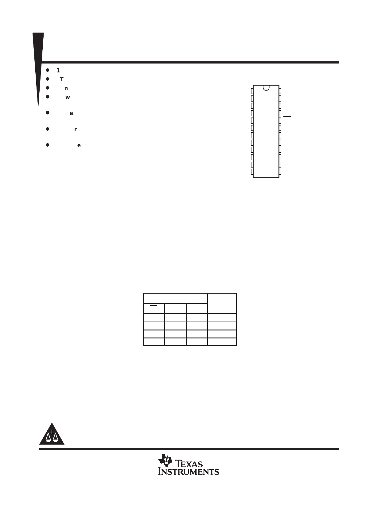
1Q
2Q
3Q
4Q
GND
GND
GND
GND
5Q
6Q
7Q
8Q
1D
2D
3D
4D
OE
(ECL)
V
CC
V
EE
CLK(TTL)
5D
6D
7D
8D
DW OR NT PACKAGE
(TOP VIEW)
PRODUCTION DATA information is current as of publication date.
Products conform to specifications per the terms of Texas Instruments
standard warranty. Production processing does not necessarily include
testing of all parameters.
Copyright 1999, Texas Instruments Incorporated
SN10KHT5578
OCTAL TTL-TO-ECL TRANSLATOR WITH D-TYPE
EDGE-TRIGGERED FLIP-FLOPS AND OUTPUT ENABLE
SDZS014A – APRIL 1990 – REVISED JANUARY 1999
2
POST OFFICE BOX 655303 • DALLAS, TEXAS 75265
logic symbol
†
1D
CLK
2D
3D
4D
5D
6D
7D
8D
1Q
2Q
3Q
4Q
5Q
6Q
7Q
8Q
17
20
24
23
22
21
16
15
14
13 12
11
10
9
4
3
2
1
1D
C1
TTL/ECL
TTL/ECL
EN
OE
†
This symbol is in accordance with ANSI/IEEE Std 91-1984 and IEC Publication 617-12.
logic diagram (positive logic)
1D
CLK
2D
3D
4D
5D
6D
7D
8D
1Q
2Q
3Q
4Q
5Q
6Q
7Q
8Q
20
17
24
23
22
21
16
15
14
13
12
11
10
9
4
3
2
1
OE
TTL/ECL
TTL/ECL
TTL/ECL
TTL/ECL
TTL/ECL
TTL/ECL
TTL/ECL
TTL/ECL
TTL/ECL
C1
1D
C1
1D
1D
1D
1D
1D
1D
C1
C1
C1
C1
C1
C1
1D

SN10KHT5578
OCTAL TTL-TO-ECL TRANSLATOR WITH D-TYPE
EDGE-TRIGGERED FLIP-FLOPS AND OUTPUT ENABLE
SDZS014A – APRIL 1990 – REVISED JANUARY 1999
3
POST OFFICE BOX 655303 • DALLAS, TEXAS 75265
absolute maximum ratings over operating ambient temperature range (unless otherwise noted)
†
Supply voltage range, V
CC
–0.5 V to 7 V. . . . . . . . . . . . . . . . . . . . . . . . . . . . . . . . . . . . . . . . . . . . . . . . . . . . . . . . . .
Supply voltage range, V
EE
–8 V to 0 V. . . . . . . . . . . . . . . . . . . . . . . . . . . . . . . . . . . . . . . . . . . . . . . . . . . . . . . . . . . .
Input voltage range (TTL) (see Note 1) –1.2 V to 7 V. . . . . . . . . . . . . . . . . . . . . . . . . . . . . . . . . . . . . . . . . . . . . . .
Input voltage range (ECL) V
EE
to 0 V. . . . . . . . . . . . . . . . . . . . . . . . . . . . . . . . . . . . . . . . . . . . . . . . . . . . . . . . . . . . .
Input current range (TTL) –30 mA to 5 mA. . . . . . . . . . . . . . . . . . . . . . . . . . . . . . . . . . . . . . . . . . . . . . . . . . . . . . . .
Current out of any output 50 mA. . . . . . . . . . . . . . . . . . . . . . . . . . . . . . . . . . . . . . . . . . . . . . . . . . . . . . . . . . . . . . . . .
Package thermal impedance, θ
JA
(see Note 2): DW package 81°C/W. . . . . . . . . . . . . . . . . . . . . . . . . . . . . . . .
NT package 67°C/W. . . . . . . . . . . . . . . . . . . . . . . . . . . . . . . . .
Storage temperature range –65°C to 150°C. . . . . . . . . . . . . . . . . . . . . . . . . . . . . . . . . . . . . . . . . . . . . . . . . . . . . . . .
†
Stresses beyond those listed under “absolute maximum ratings” may cause permanent damage to the device. These are stress ratings only and
functional operation of the device at these or any other conditions beyond those indicated under “recommended operating conditions” is not implied.
Exposure to absolute-maximum-rated conditions for extended periods may affect device reliability .
NOTES: 1. The TTL input voltage ratings may be exceeded provided the input current ratings are observed.
2. The package thermal impedance is calculated in accordance with JESD 51, except for through-hole packages, which use a trace
length of zero.
recommended operating conditions
MIN NOM MAX UNIT
V
CC
TTL supply voltage 4.5 5 5.5 V
V
EE
ECL supply voltage –4.94 –5.2 –5.46 V
V
IH
TTL high-level input voltage 2 V
0°C –1170 –840 mV
V
IH
ECL high-level input voltage
‡
25°C –1130 –810 mV
75°C –1070 –735 mV
V
IL
TTL low-level input voltage 0.8 V
0°C –1950 –1480 mV
V
IL
ECL low-level input voltage
‡
25°C –1950 –1480 mV
75°C –1950 –1450 mV
I
IK
TTL input clamp current –18 mA
T
A
Operating ambient temperature (see Note 3) 0 75 °C
‡
The algebraic convention, in which the least positive (most negative) value is designated minimum, is used in this data sheet for logic levels only .
NOTE 3: Each 10KH-series circuit has been designed to meet the dc specifications shown in the electrical characteristics table after thermal
equilibrium has been established. The circuit is in a test socket or mounted on a printed circuit board, and transverse airflow greater than
500 linear ft/min is maintained.

SN10KHT5578
OCTAL TTL-TO-ECL TRANSLATOR WITH D-TYPE
EDGE-TRIGGERED FLIP-FLOPS AND OUTPUT ENABLE
SDZS014A – APRIL 1990 – REVISED JANUARY 1999
4
POST OFFICE BOX 655303 • DALLAS, TEXAS 75265
electrical characteristics over recommended operating ambient temperature range (unless
otherwise noted)
PARAMETER TEST CONDITIONS MIN
TYP
†
MAX UNIT
V
IK
CLK and D inputs VCC = 4.5 V, VEE = –4.94 V, II = –18 mA –1.2 V
I
I
CLK and D inputs VCC = 5.5 V, VEE = –5.46 V, VI = 7 V 0.1 mA
CLK and D inputs VCC = 5.5 V, VEE = –5.46 V, VI = 2.7 V 20
VCC = 5.5 V, VEE = –5.46 V, VI = –840 mV 0°C 350
I
IH
OE input VCC = 5.5 V, VEE = –5.46 V, VI = –810 mV 25°C 350
µ
A
VCC = 5.5 V, VEE = –5.46 V, VI = –735 mV 75°C 350
CLK and D inputs VCC = 5.5 V, VEE = –5.46 V, VI = 0.5 V –0.5 mA
0°C 0.5
I
IL
OE input VCC = 5.5 V, VEE = –5.46 V, VI = –1950 mV 25°C 0.5 µA
75°C 0.5
0°C –1020 –840
V
OH
‡
VCC = 4.5 V, VEE = –5.2 V ± 5%, See Note 4 25°C –980 –810 mV
75°C –920 –735
0°C –1950 –1630
V
OL
‡
VCC = 4.5 V, VEE = –5.2 V ± 5%, See Note 4 25°C –1950 –1630 mV
75°C –1950 –1600
I
CCH
VCC = 5.5 V, VEE = –5.46 V 17.5 25 mA
I
CCL
VCC = 5.5 V, VEE = –5.46 V 15 22 mA
I
EE
VCC = 5.5 V, VEE = –5.46 V –104 –149 mA
C
i
VCC = 5 V, VEE = –5.2 V, f = 10 MHz 4 pF
†
All typical values are at VCC = 5 V, VEE = –5.2 V, TA = 25°C.
‡
The algebraic convention, in which the least positive (most negative) value is designated minimum, is used in this data sheet for logic levels only .
NOTE 4: Outputs are terminated through a 50-Ω resistor to –2 V.
timing requirements over recommended operating conditions
MIN MAX UNIT
f
clock
Clock frequency 180 MHz
High 4
twPulse duration, CLK
Low 4
ns
p
High 1.5
tsuSetup time, data before CLK↑
Low 2.5
ns
High 1
thHold time, data after CLK↑
Low 1
ns
switching characteristics over recommended ranges of supply voltage and operating ambient
temperature (see Figure 1)
PARAMETER
FROM
(INPUT)
TO
(OUTPUT)
MIN TYP†MAX UNIT
f
max
180 MHz
t
PLH
0.8 2.2 4
t
PHL
CLK
Q
0.8 2.1 3.8
ns
t
PLH
0.5 1.4 3.2
t
PHL
OE
Q
0.5 1.7 3.3
ns
t
r
Y 1.5 ns
t
f
Y 1.5 ns
†
All typical values are at VCC = 5 V, VEE = –5.2 V, TA = 25°C.

SN10KHT5578
OCTAL TTL-TO-ECL TRANSLATOR WITH D-TYPE
EDGE-TRIGGERED FLIP-FLOPS AND OUTPUT ENABLE
SDZS014A – APRIL 1990 – REVISED JANUARY 1999
5
POST OFFICE BOX 655303 • DALLAS, TEXAS 75265
PARAMETER MEASUREMENT INFORMATION
–2 V
50 Ω
OUTPUT LOAD CIRCUIT
From Output Under Test
3 V
0 V
3 V
0 V
1.5 V 1.5 V
1.5 V
1.5 V
t
w
PULSE DURATION
High-Level
Pulse
Low-Level
Pulse
t
su
3 V
0 V
1.5 V
t
h
1.5 V 1.5 V
3 V
0 V
SETUP AND HOLD TIMES
Timing
Input
Data
Input
TTL-INPUT PROPAGATION DELAY TIMES
t
PHL
t
PLH
ECL-OUTPUT PROPAGATION DELAY TIMES
V
OH
V
OL
t
f
t
r
–890 mV
–1690 mV
50%
50%
20%20%
50% 50%
80% 80%
Output Enable
(see Note B)
ECL Output Waveform 1
(see Notes C and D)
50%
3 V
1.5 V
0 V
1.5 V
50%
In–Phase
Output
Out-of-Phase
Output
V
OH
V
OH
V
OL
V
OL
Input
(see Note A)
t
PLH
t
PHL
NOTES: A. For TTL inputs, input pulses are supplied by generators having the following characteristics: PRR ≤ 10 MHz, ZO = 50 Ω,
tr = 2.5 ns, tf = 2.5 ns.
B. For ECL inputs, input pulses are supplied by generators having the following characteristics: PRR ≤ 10 MHz, ZO = 50 Ω,
tr = 1.5 ns, tf = 1.5 ns.
C. Waveform 1 is for an output with internal conditions such that the output is high except when disabled by OE
.
D. The outputs are measured one at a time with one input transition per measurement.
Figure 1. Load Circuit and Voltage Waveforms

IMPORTANT NOTICE
T exas Instruments and its subsidiaries (TI) reserve the right to make changes to their products or to discontinue
any product or service without notice, and advise customers to obtain the latest version of relevant information
to verify, before placing orders, that information being relied on is current and complete. All products are sold
subject to the terms and conditions of sale supplied at the time of order acknowledgement, including those
pertaining to warranty, patent infringement, and limitation of liability.
TI warrants performance of its semiconductor products to the specifications applicable at the time of sale in
accordance with TI’s standard warranty. Testing and other quality control techniques are utilized to the extent
TI deems necessary to support this warranty. Specific testing of all parameters of each device is not necessarily
performed, except those mandated by government requirements.
CERT AIN APPLICATIONS USING SEMICONDUCTOR PRODUCTS MAY INVOLVE POTENTIAL RISKS OF
DEATH, PERSONAL INJURY, OR SEVERE PROPERTY OR ENVIRONMENTAL DAMAGE (“CRITICAL
APPLICATIONS”). TI SEMICONDUCTOR PRODUCTS ARE NOT DESIGNED, AUTHORIZED, OR
WARRANTED TO BE SUITABLE FOR USE IN LIFE-SUPPORT DEVICES OR SYSTEMS OR OTHER
CRITICAL APPLICATIONS. INCLUSION OF TI PRODUCTS IN SUCH APPLICA TIONS IS UNDERST OOD TO
BE FULLY AT THE CUSTOMER’S RISK.
In order to minimize risks associated with the customer’s applications, adequate design and operating
safeguards must be provided by the customer to minimize inherent or procedural hazards.
TI assumes no liability for applications assistance or customer product design. TI does not warrant or represent
that any license, either express or implied, is granted under any patent right, copyright, mask work right, or other
intellectual property right of TI covering or relating to any combination, machine, or process in which such
semiconductor products or services might be or are used. TI’s publication of information regarding any third
party’s products or services does not constitute TI’s approval, warranty or endorsement thereof.
Copyright 1998, Texas Instruments Incorporated
 Loading...