

Page 1
查询PT6363供应商
PT6360 Series
11 A 12-V Input Adjustable
Integrated Switching Regulator
Features
• 12 V Input
• 11 A Output Current
• DSP Compatible
• >90 % Efficiency
• Adjustable Output Voltage
• On/Off Inhibit Function
• Over-Current Protection
Description
The PT6360 Excalibur™ series of integrated
switching regulators (ISRs) combines outstanding power density with a comprehensive list of
features. They are an ideal choice for applications
where board space is a premium and performance
cannot be compromised. These modules provide up
to 11 A of output current, yet are housed in a lowprofile, 12-pin, package that is almost half the
size of the previous product generation. The integral copper case construction requires no heatsink,
and offers the advantages of solderability and a
small footprint (0.64 in² for suffix ‘N’). Both
through-hole and surface mount pin configurations are available.
The PT6360 series operates from a 12-V input
bus and provides a convenient point-of-load power
source for the industry’s latest high-performance
DSPs and microprocessors. The series includes
output voltage options as low as 1.0 VDC.
Other features include external output voltage
adjustment, on/off inhibit, short circuit protection,
and an output remote sense.
SLTS179A - JANUARY 2003 - REVISED APRIL 2003
• Output Remote Sense
• Low-Profile (8 mm)
• Small Footprint
• Surface Mountable
• IPC Lead Free 2
Ordering Information
PT6361H = 5.0 Volts
PT6362H = 3.3 Volts
PT6363H = 2.5 Volts
PT6364H = 1.8 Volts
PT6365H = 1.5 Volts
PT6366H = 1.2 Volts
PT6367H = 1.0 Volts
PT Series Suffix
Case/Pin Order Package
Configuration Suffix Code
Vertical N (EPH)
Horizontal A (EPJ)
SMD C (EPK)
(Reference the applicable package code drawing for the dimensions and PC board layout)
(PT1234x)
(0.64 in², Suffix ‘N’)
Pin-Out Information
Pin Function
1 Inhibit*
2V
in
3V
in
4V
in
5 GND
6 GND
7 GND
8 GND
9V
out
10 V
out
11 (+)Sense
12 Vo Adjust
* Denotes negative logic:
Open = Output enabled
Ground = Output disabled
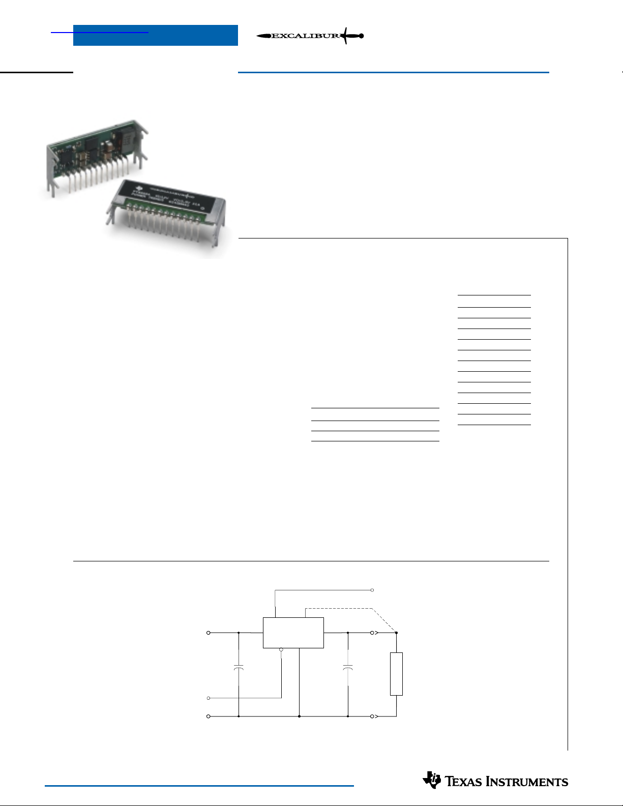
Standard Application
12
V
IN
C
IN
560 µF
(Required)
Inhibit
GND
For technical support and more information, see inside back cover or visit www.ti.com
2–4
PT6360
+
1
11
5–8
C
330 µF
(Optional)
OUT
9–10
(+)Sense
+
Vo Adjust
V
OUT
GND
L
O
A
D
Cin= Required 560 µF
C
= Optional 330 µF
out
Page 2
PT6360 Series
11 A 12-V Input Adjustable
Integrated Switching Regulator
Performance Specifications (Unless otherwise stated, T
=25 °C, Vin =12 V, Cin =560 µF, C
a
SLTS179A - JANUARY 2003 - REVISED APRIL 2003
=0 µF, and Io =Iomax)
out
PT6360 SERIES
Characteristics Symbols Conditions Min Typ Max Units
Output Current I
Input Voltage Range V
o
in
Vin =12 V V
Over Io range 10.8 — 13.2 V
< 3.3 V 0 — 11
o
V
≥ 3.3 V 0 — 10
o
Set-Point Voltage Tolerance Vo tol — — ±2 %V
Temperature Variation ∆Reg
Line Regulation ∆Reg
Load Regulation ∆Reg
Total Output Variation ∆Reg
temp
line
load
tot
Efficiency η I
V
Ripple (pk-pk) V
o
r
Transient Response 1 A/µs load step, 50 to 100 % Iomax,
t
tr
∆V
Over-Current Threshold I
tr
TRIP
Output Voltage Adjust Vo adj With Vo Adjust — ±15
Switching Frequency ƒ
Inhibit Control (pin1) Referenced to GND (pins 5–8)
Input High Voltage V
Input Low Voltage
Input Low Current
s
IH
V
IL
I
IL Pin 1 to GND — –10 — µA
–40 °C <Ta < +85 °C — ±0.5 — %V
Over Vin range — ±3 — mV
Over Io range — ±5 — mV
Includes set-point, line, load,
–40 °C ≤ Ta ≤ +85 °C
=8 A PT6361 ( 5 V) — 93 —
o
20 MHz bandwidth V
=330 µF
C
out
PT6362 (3.3 V) — 91 —
PT6363 (2.5 V) — 90 —
PT6364 (1.8 V) — 87 — %
PT6365 (1.5 V) — 85 —
PT6366 (1.2 V) — 82 —
PT6367 (1.0 V) — 80 —
= 5.0 V — 50 —
o
= 3.3 V — 25 — mV
V
o
V
≤ 2.5 V — 15 —
o
Recovery Time — 50 — µSec
Vo over/undershoot — 70 — mV
——±3%V
Reset, followed by auto-recovery — 16 — A
(1)
—%
Over Vin and Io ranges 300 350 400 kHz
2 — Open
–0.2 — 0.3
(2)
Standby Input Current Iin standby Pin 1 to GND — 5 — mA
External Input Capacitance C
External Output Capacitance C
Operating Temperature Range T
Solder Reflow Temperature T
Storage Temperature T
Reliability MTBF Per Bellcore TR-332
Mechanical Shock Mil-STD-883D, Method 2002.3
Mechanical Vibration Mil-STD-883D, Method 2007.2,
in
out
a
reflow
s
Over Vin range –40 — 85
Surface temperature of pins or case — — 215
— –40 — 125 °C
50% stress, Ta =40°C, ground benign
Half Sine, mounted to a fixture
20-2000 Hz, PCB mounted
(3)
560
0 330
——µF
(4)
5,000 µF
(5)
(6)
8.0 — — 10
— 500 — G’s
— 20
(7)
—G’s
Weight — — — 10 — grams
Flammability — Materials meet UL 94V-0
Notes:
(1) This is a typical value. For the adjustment limits of a specific model consult the related application note on output voltage adjustment.
(2) The Inhibit control (pin 1) has an internal pull-up to Vin, and if left open-circuit the module will operate when input power is applied. A small low-
leakage (<100 nA) MOSFET is recommended to control this input. See application notes for more information.
(3) A 560 µF electrolytic input capacitor is required for proper operation. The capacitor must be rated for a minimumm of 1.3 Arms of ripple current.
(4) An external output capacitor is not required for basic operation. Adding 330µF of distributed capacitance at the load will improve the transient response,
and reduce output ripple voltage.
(5) See SOA curves or consult factory for the appropriate derating.
(6) During solder reflow of SMD package version do not elevate the module case, pins, or internal component temperatures above a peak of 215 °C. For
further guidance refer to the application note, “Reflow Soldering Requirements for Plug-in Power Surface Mount Products,” (SLTA051).
(7) The case pins on the through-hole package types (suffixes N & A) must be soldered. For more information see the applicable package outline drawing.
A
o
o
o
pp
V
°C
°C
6
Hrs
For technical support and more information, see inside back cover or visit www.ti.com
Page 3
PT6360 Series
)
)
)
11 A 12-V Input Adjustable
Integrated Switching Regulator
Pin Descriptions
Vin: The positive supply voltage input for the module
with respect to the common GND.
Vout: This is the regulated output voltage from the module with respect to the common GND.
GND: The common node to which the input, output, and
external control signals are referenced.
Inhibit*: This is an open-collector (open-drain) negative
logic input, that is referenced to GND. Driving this pin to
GND disables the module’s output voltage. If Inhibit* is
left open-circuit, the output will be active whenever a
valid input source is applied.
SLTS179A - JANUARY 2003 - REVISED APRIL 2003
Vo Adjust: This pin is used to trim the output voltage to a
value within the range of approximately ±15 % of nominal.
The adjustment method uses an external resistor. The
resistor is connected from V
Adjust to either the GND
o
or (+)Sense, in order to adjust the output either up or
down, respectively.
(+)Sense: An external remote sense input is provided to
allow the regulation circuit to compensate for voltage
drop between the module and the load. For optimal
voltage accuracy (+)Sense should be connected to V
out
. If
desired, (+)Sense may also be left open circuit.
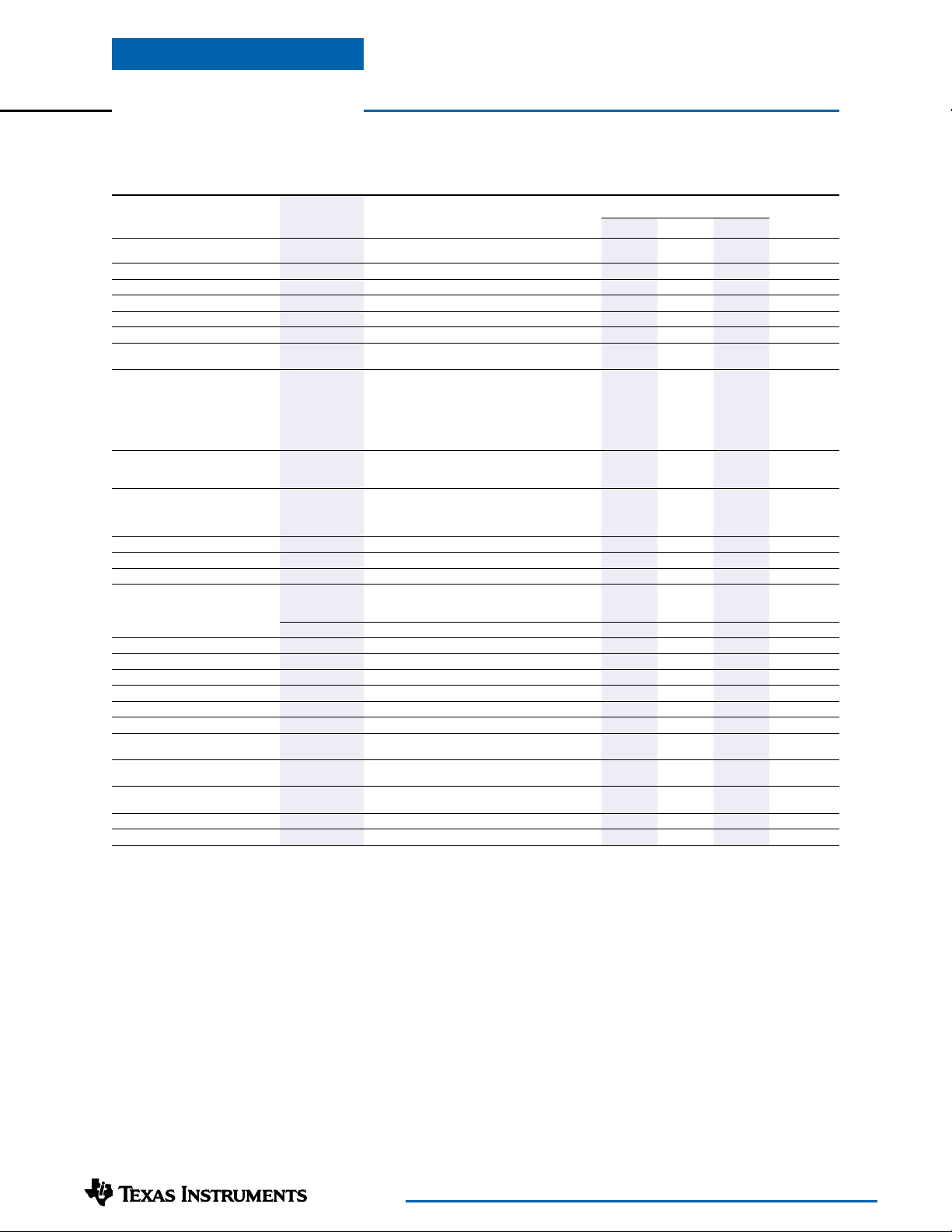
Typical Characteristics
Performance Data; Vin =12 V (See Note A)
Efficiency vs Output Current
100
90
80
70
Efficiency - %
60
50
0246810
Output Ripple vs Output Current
100
80
60
40
Ripple - mV
20
Iout (A
PT6361
PT6362
PT6363
PT6364
PT6365
PT6366
PT6367
PT6361
PT6362
PT6363
PT6364
PT6365
PT6366
PT6367
Power Dissipation vs Output Current
5
4
3
2
Pd - Watts
1
0
0246810
Iout (A
PT6361
PT6362
PT6363
PT6364
PT6365
PT6366
PT6367
0
0246810
Iout (A
Note A: Characteristic data has been developed from actual products tested at 25°C. This data is considered typical data for the ISR.
For technical support and more information, see inside back cover or visit www.ti.com
Page 4
)
)
)
)
)
PT6360 Series
11 A 12-V Input Adjustable
Integrated Switching Regulator
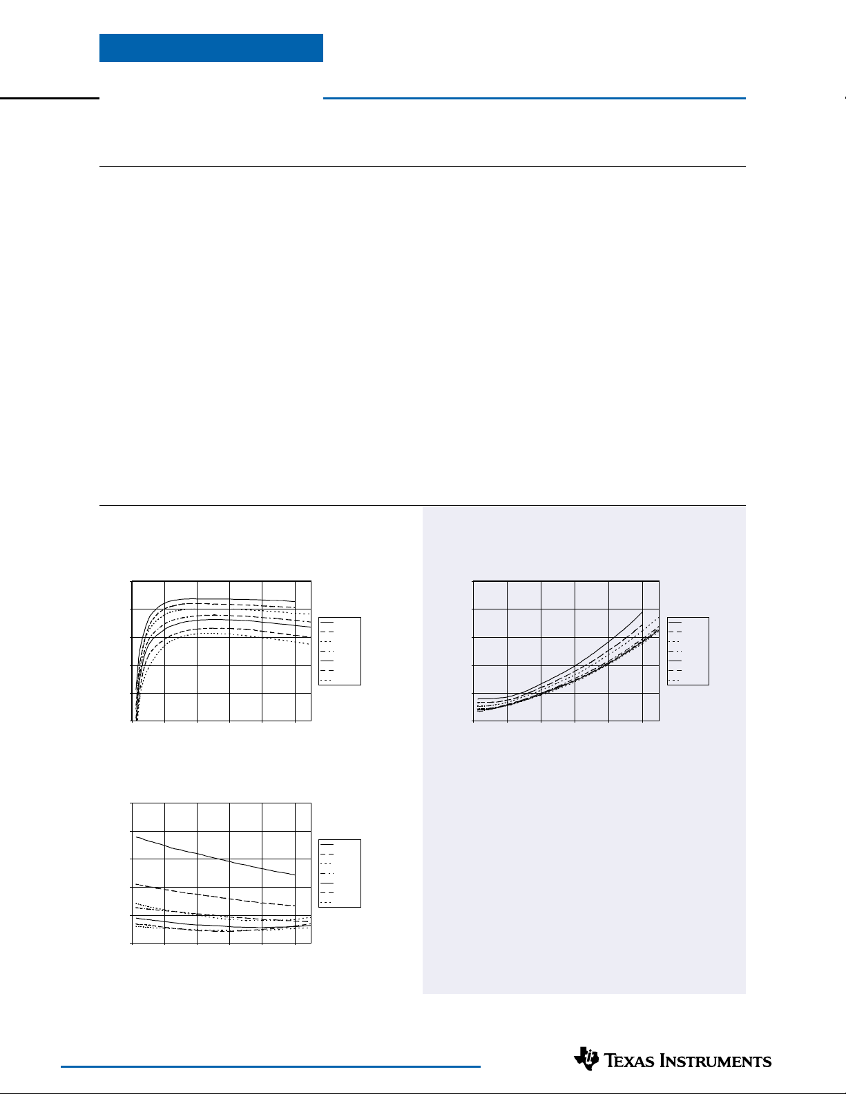
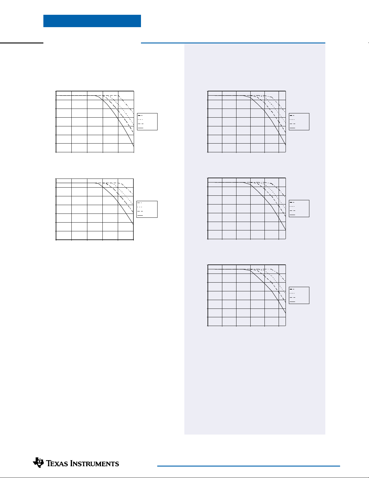
Safe Operating Curves, Vin =12 V (See Note B)
PT6361, Vo =5 V, 0–10 A
90
80
70
60
50
40
Ambient Temperature (°C)
30
20
0246810
PT6362, Vo =3.3 V, 0–10 A
90
80
70
60
50
40
Ambient Temperature (°C)
30
20
0246810
Iout (A
Iout (A
Airflow
200LFM
120LFM
60LFM
Nat conv
Airflow
200LFM
120LFM
60LFM
Nat Conv
SLTS179A - JANUARY 2003 - REVISED APRIL 2003
Safe Operating Curves, Vin =12 V (See Note B)
PT6363, Vo =2.5 V, 0–11 A
90
80
70
60
50
40
Ambient Temperature (°C)
30
20
0246810
PT6364, Vo =1.8 V, 0–11 A
90
80
70
60
50
40
Ambient Temperature (°C)
30
20
0246810
Iout (A
Iout (A
Airflow
200LFM
120LFM
60LFM
Nat conv
Airflow
200LFM
120LFM
60LFM
Nat conv
PT6366, Vo =1.2 V, 0–11 A
90
80
70
60
50
40
Ambient Temperature (°C)
30
20
0246810
Iout (A
Airflow
200LFM
120LFM
60LFM
Nat conv
Note B: SOA curves represent operating conditions at which internal components are at or below manufacturer’s maximum rated operating temperatures.
For technical support and more information, see inside back cover or visit www.ti.com
Page 5
Application Notes
PT6360 Series
Operating Features and System Considerations
for the PT6360 Regulator Series
The PT6360 is a series of integrated switching regulators
(ISRs) that operate off a 12-V input to provide stepdown voltage conversion for output loads of up to 11 A.
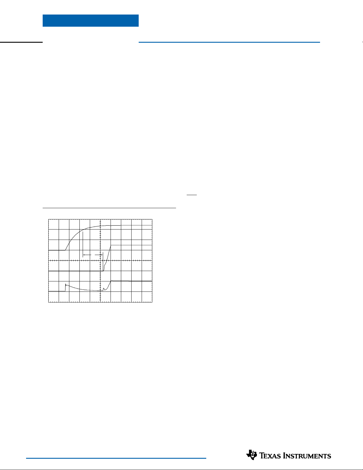
Power up & Soft-Start Timing
Following either the application of a valid input source
voltage, or the removal of a ground signal to the Inhihit
control pin (with input power applied), the regulator will
initiate a soft-start power up. A soft start slows the rate at
which the output voltage rises and introduces a short time
delay, td (approx. 10 ms), into the power-up sequence.
Figure 1-1 shows the power-up characteristic of a PT6363
(2.5-V output) with an 8.3-A load. Note that the initial
step of input current when the input voltage begins to
rise is the input capacitor(s) charging.
Figure 1-1
Vin (5V/Div)
Vo (1V/Div)
t
d
Output Remote Sense
The (+)Sense pin allows the regulator to compensate for
limited amounts of ‘IR’ voltage drop in the positive output
connection resistance. This is the voltage drop incurred
in the PCB trace between Vout (pins 9 & 10) of the regulator and the load some distance away. Connecting (+)Sense
to the positive load terminal improves the voltage regulation at the load, particularly when the load current
fluctuates. Although not recommended, leaving (+)Sense
disconnected will not damage the regulator or the load
circuitry. An internal 10 Ω resistor, connected between
the sense pin and the output, keeps the output voltage in
regulation.
With the sense pin connected, the difference between
the voltage measured between V
regulator, and that measured from (+)Sense to GND, is
the amount of IR drop being compensated by the regulator. This should be limited to 0.3 V maximum.
Note: The remote sense feature is not designed to compensate
for the forward drop of non-linear or frequency dependent
components that may be placed in series with the converter
output. Examples include OR-ing diodes, filter inductors,
ferrite beads, and fuses. When these components are enclosed
by the remote sense connections they are effectively placed
inside the regulation control loop, which can adversely affect
the stability of the regulator.
and GND at the
out
Iin (2A/Div)
HORIZ SCALE: 5ms/Div
Over-Current Protection
To protect against load faults, these ISRs incorporate
output over-current protection. Applying a load that
exceeds the over-current threshold (see data sheet specifications) will cause the regulated output to shut down.
Following shutdown the ISR will periodically attempt to
recover by initiating a soft-start power-up. This is often
described as a “hiccup” mode of operation, whereby the
module continues in a cycle of successive shutdown and
power up until the load fault is removed. During this
period, the average current flowing into the fault is
significantly reduced. Once the fault is removed, the
converter automatically recovers and returns to normal
operation.
For technical support and more information, see inside back cover or visit www.ti.com
Page 6

Application Notes
PT6360 Series
Capacitor Recommendations for the PT6360 Series
of Integrated Switching Regulators
Input Capacitor:
The recommended input capacitance is determined by
1.3-A minimum ripple current rating and 560 µF minimum capacitance.
Ripple current and <100 mΩ equivalent series resistance
(ESR) values are the major considerations, along with
temperature, when designing with different types of
capacitors. Tantalum capacitors have a recommended
minimum voltage rating of 2 × (max. dc voltage + ac
ripple). This is necessary to insure reliability for input
voltage bus applications.
Output Capacitors:
The recommended ESR of the output capacitor is 150mΩ.
Electrolytic capacitors have marginal ripple performance
at frequencies greater than 400kHz but excellent low
frequency transient response. Above the ripple frequency,
ceramic capacitors are necessary to improve the transient
response and reduce any high frequency noise components
apparent during higher current excursions. Preferred low
ESR type capacitor part numbers are identified in Table
2-1.
Tantalum Capacitors
Tantalum type capacitors can be used for the output but
only the AVX TPS, Sprague 593D/594/595 or Kemet
T495/T510 series. These capacitors are recommended
over many other tantalum types due to their higher rated
surge, power dissipation, and ripple current capability.
As a caution the TAJ series by AVX is not recommended.
This series has considerably higher ESR, reduced power
dissipation, and lower ripple current capability. The TAJ
series is less reliable than the AVX TPS series when determining power dissipation capability. Tantalum or Oscon®
types are recommended for applications where ambient
temperatures fall below 0 °C.
Capacitor Table
Table 2-1 identifies the characteristics of capacitors from
a number of vendors with acceptable ESR and ripple
current (rms) ratings. The number of capacitors required
at both the input and output buses is identified for each
capacitor type.
This is not an extensive capacitor list. Capacitors from other
vendors are available with comparable specifications. Those listed
are for guidance. The RMS ripple current rating and ESR
(Equivalent Series Resistance at 100 kHz) are critical parameters necessary to insure both optimum regulator performance
and long capacitor life.
Table 2-1: Input/Output Capacitors
seireS
SS
(tnuoMecafruS)
(tnuoMecafruS)
(1) N/R –Not recommended. The voltage rating does not meet the minimum operating limits.
(2) Recommended Input capacitor when Vo<2.6 V; lower RMS mA required .
/rodneVroticapaC
cinosanaP
)laidaR(CF
)gtMecafruS(KF/CF
noc-imehCdetinU
seireSVXL/ZXL
)gtMecafruS(YVM
nocihciN
seireSMP
:noc-sO
)tnuoMecafrus(PVS
seireSVSdlO
mulatnaTXVA
)tgtMecafruS(SPT
mulatnaTtemeK
seireS594T/025T
mulatnaTeugarpS
seireSD495
scitsiretcarahCroticapaCytitnauQ
gnikroW
egatloV
V53
V52
V52
V05
V53
V53
V53
V52
V53
V52
V53
V01
V61
V01
V01
V01
V3.6
V01033540.0 Ω Am0632L2.7
)Fµ(eulaVtnelaviuqE)RSE(
086
033
0001
0001
086
086
086
033
065
0021
028
033
033
033
033
033
022
1.0 Ω
3700 Ω
51.0 Ω
60.0 Ω
70.0 Ω
340.0 Ω
090.0 Ω
830.0 Ω
060.0 Ω
730.0 Ω
860.0 Ω
840.0 Ω
930.0 Ω
830.0 Ω
520.0 Ω
610.0 Ω
040.0 Ω
ecnatsiseRseireS
mumixaMC°501
elppiR
)smrI(tnerruC
Am5561
Am557
Am0961
Am0161
Am0011
Am0661
Am0501
Am076
Am0631
Am0041
Am0731
Am0053
Am0074
Am0052>
Am0003>
Am0061
Am0002>
eziSlacisyhP
tupnI
)mm(
5.21 × 02
01 × 5.21
61 × 51
61 × 5.61
5.21 × 5.31
5.21 × 02
01 × 61
01 × 3.01
61 × 51
61 × 51
81 × 51
01 × 5.01
11 × 21
× W7.5
× H1.4
× L3.7
× H0.4
× W6
× H1.4
1
R/N
1
1
1
1
1
R/N
1
1
1
R/N
2
L3.7
R/N
R/N
W3.4
R/N
R/N
R/N
tuptuO
suB
suB
1
)1(
1
1
1
2(
)
1
1
)2(
1
)1(
1
1
1
1
)1(
1
1
)1(
1
)1(
1
)1(
1
)1(
1
)1(
1T2R0100X733D495
M033SS01 V(
186V1CFUEE
133E1CFUEE
S201E1CFUEE
M201H1KFVEE
Q186V1KFVEE )V6.2<oV(
o
M033PVS61
SA010M733X025
6HHM165V1MPU
6HHM221E1MPU
6HHM128V1MPU
)V1.5<
0010R010M733ESPT V(
0600R010M733VSPT V(
SA0010M722X594T
rebmuNtraProdneV
LL02X21M186BV53ZXL
LL02X61M201BV53VXL V6.2<oV( )
PT01X01M133CV52YVM
)V1.5<
o
)V1.5<
o
For technical support and more information, see inside back cover or visit www.ti.com
Page 7

Application Notes
PT6360 Series
Adjusting the Output Voltage of the PT6360 Series
of Integrated Switching Regulators
The output voltage of the PT6360 series of power modules
may be adjusted higher or lower than the pre-set voltage
with the addition of a single external resistor. Table 3-1
gives the allowable adjustment range for each model of the
series as Va (min) and Va (max). The value of the external
resistor can either be calculated using the formulas given
below, or simply selected from the range of values given
in Table 3-2. Refer to Figure 3-1 for the placement of
the required resistor. Use the resistor R
and the resistor (R
) to down.
2
to adjust up,
1
Adjust Up: An increase in the output voltage is obtained
by adding a resistor R
, between Vo adjust (pin 12) and
2
GND (pins 5-8).
Adjust Down: Add a resistor (R
), between Vo adjust (pin 12)
1
and (+)Sense (pin 11).
Figure 3-1
11
+V
IN
C
IN
560 µF
(Req'd)
2–4
Vin Vo
Inh
1
+
PT6360
5–812
(+)Sense
Vo(adj)GND
9–10
(R1)
Adj Down
R
2
Adjust Up
C
OUT
330 µF
(Optional)
+V
O
COMCOM
The values of (R1) [adjust down], and R2 [adjust up],
can be calculated using the following formulas. Refer to
Figure 3-1 for the placement of the required resistor;
either (R
) or R2 as appropriate.
1
(R1) =
R
2
=
R
(Va – 0.8)
o
Vo – V
0.8 R
o
V
– V
a
o
a
– R
– R
kΩ
s
kΩ
s
Where: Vo= Original output voltage
= Adjusted output voltage
V
a
= The resistance value from Table 3-1
R
o
= The series resistance from Table 3-1
R
s
Notes:
1. Use a 1% (or better) tolerance resistor in either the (R1)
location. Place the resistor as close to the ISR as
or R
2
possible.
2. Never connect capacitors from Vo Adjust to either GND or
. Any capacitance added to the Vo Adjust pin will affect
V
out
the stability of the ISR.
3. If the remote sense feature is not being used, the adjust
resistor (R1) can also be connected to V
, (pins 9–10)
out
instead of (+)Sense.
Table 3-1
ISR OUTPUT VOLTAGE ADJUSTMENT RANGE AND FORMULA PARAMETERS
Series Pt. No. PT6361 PT6362 PT6363 PT6364 PT6365 PT6366 PT6367
Vo (nom) 5.0 V 3.3 V 2.5 V 1.8 V 1.5 V 1.2 V 1.0 V
Va (min) 3.35 V 2.6 V 2.0 V 1.52 V 1.31 V 1.1 V 0.95 V
Va (max) 5.5 V 3.63 V 2.8 V 2.1 V 1.82 V 1.52 V 1.32 V
ΩΩ
Ro (k
Ω) 10.0 10.2 10.7 10.2 9.76 10.0 10.2
ΩΩ
ΩΩ
Rs (k
Ω) 15.0 24.9 24.9 24.9 24.9 24.9 24.9
ΩΩ
For technical support and more information, see inside back cover or visit www.ti.com
Page 8

Application Notes
continued
PT6360 Series
Table 3-2
ISR ADJUSTMENT RESISTOR VALUES
Series Pt. No. PT6361 PT6362 PT6363 PT6364 PT6365 PT6366 PT6367
Vo (nom) 5.0 V 3.3 V 2.5 V 1.8 V 1.5 V 1.2 V 1.0 V
Va (req.d)
5.50 1.0 kΩ
5.40 5.0 kΩ
5.30 11.7 kΩ
5.20 25.0 kΩ
5.10 65.0 kΩ
5.00
4.90 (395.0) kΩ
4.80 (185.0) kΩ
4.70 (115.0) kΩ
4.60 (80.0) kΩ
4.50 (59.0) kΩ
4.40 (45.0) kΩ
4.30 (35.0) kΩ
4.20 (27.5) kΩ
4.10 (21.7) kΩ
4.00 (17.0) kΩ
3.90 (13.2) kΩ
3.80 (10.0) kΩ
3.70 (7.3) kΩ
3.60 (5.0) kΩ 2.3 kΩ
3.55 (4.0) kΩ 7.7 kΩ
3.50 (3.0) kΩ 15.9 kΩ
3.45 (2.1) kΩ 29.5 kΩ
3.40 (1.3) kΩ 56.7 kΩ
3.35 (0.5) kΩ 138.0 kΩ
3.30
3.25 (475.0) kΩ
3.20 (220.0) kΩ
3.15 (135.0) kΩ
3.10 (92.4) kΩ
3.05 (66.9) kΩ
3.00 (49.9) kΩ
2.95 (37.5) kΩ
2.90 (28.6) kΩ
2.85 (21.6) kΩ
2.80 (15.9) kΩ
2.75 (11.3) kΩ
2.70 (7.4) kΩ
2.65 (4.1) kΩ
2.60 (1.3) kΩ
R1 = (Blue) R2 = Black
Va (req.d)
2.800 3.6 kΩ
2.750 9.3 kΩ
2.700 17.9 kΩ
2.650 32.2 kΩ
2.600 60.7 kΩ
2.550 146.0 kΩ
2.500
2.450 (328.0) kΩ
2.400 (146.0) kΩ
2.350 (85.7) kΩ
2.300 (55.3) kΩ
2.250 (37.2) kΩ
2.200 (25.0) kΩ
2.150 (16.4) kΩ
2.100 (9.9) kΩ 2.3 kΩ
2.050 (4.8) kΩ 7.7 kΩ
2.000 (0.8) kΩ 15.9 kΩ
1.950 29.5 kΩ
1.900 56.7 kΩ
1.850 138.0 kΩ
1.800 1.1 kΩ
1.750 (169.0) kΩ 6.3 kΩ
1.700 (66.9) kΩ 14.1 kΩ
1.650 (32.9) kΩ 27.2 kΩ
1.600 (15.9) kΩ 53.2 kΩ
1.550 (5.7) kΩ 131.0 kΩ
1.500 1.8 kΩ
1.475 (239.0) kΩ 4.2 kΩ
1.450 (102.0) kΩ 7.1 kΩ
1.425 (56.4) kΩ 10.7 kΩ
1.400 (33.7) kΩ 15.1 kΩ
1.375 (20.0) kΩ 20.8 kΩ
1.350 (10.9) kΩ 28.4 kΩ
1.325 (4.4) kΩ 39.1 kΩ
1.300 55.1 kΩ 2.3 kΩ
1.275 81.8 kΩ 4.8 kΩ
1.250 135.0 kΩ 7.7 kΩ
1.225 295.0 kΩ 11.4 kΩ
1.200 15.9 kΩ
1.175 (125.0) kΩ 21.7 kΩ
1.150 (45.1) kΩ 29.5 kΩ
1.125 (18.4) kΩ 40.4 kΩ
1.100 (5.1) kΩ 56.7 kΩ
1.075 83.9 kΩ
1.050 138.0 kΩ
1.025 302.0 kΩ
1.000
0.975 (46.5) kΩ
0.950 (5.7) kΩ
For technical support and more information, see inside back cover or visit www.ti.com
Page 9

Application Notes
PT6360 Series
Using the Inhibit Control of the PT6360 Series of
Integrated Switching Regulators
The PT6360 series of integrated switching regulators
(ISRs) provide step-down voltage conversion for output
loads of up to 11 A. For applications that require the
output voltage to be held off, these ISRs incorporate an
Inhibit* control (pin 1). The Inhibit* control input can be
used for power-up sequencing or whenever there is a
requirement for the output voltage from the ISR to be
turned off.
The ISR functions normally with pin 1 open circuit,
providing a regulated output whenever a valid source
voltage is applied between V
(pins 2–3) and GND (pins
in
5–8). When a low-level ground signal is applied to pin 1,
the regulator output is turned off 2 and the input current
is significantly reduced 4.
Figure 4-1 shows the typical application of the Inhibit*
function. Note the discrete transistor, Q
. The Inhibit*
1
control has its own internal pull-up to Vin potential. An
open-collector or open-drain device is recommended to
control this input 1. The voltage thresholds are given in
Table 4-1.
Table 4-1; Inhibit Control Requirements
Parameter Min Typ Max
Enable (VIH) 2.0 V — Vin
Disable (VIL) –0.1 V — +0.3 V
I
IL
— –0.5 mA —
Turn-On Time: In the circuit of Figure 4-1, turning Q
1
on
1
applies a low-voltage to the Inhibit* control (pin 1) and
2
disables the output of the regulator
off, the ISR executes a soft-start power up
. If Q1 is then turned
3
. Power up
consists of a short delay (approx. 10 msec), followed by a
period in which the output voltage rises to the full regulation voltage. The module produces a regulated output
voltage in approximately 15 msec. Figure 4-2 shows the
rise in both the output voltage and input current for a
PT6363 (2.5 V), following the turn-off of Q
off of Q
corresponds to the rise in the waveform, Q1 Vds.
1
. The turn
1
The waveforms were measured with a 12 VDC input
voltage, and 8.3-A load.
Figure 4-2
Vo (1V/Div)
Iin (2A/Div)
Q1 Vds (10V/Div)
HORIZ SCALE: 5ms/Div
Figure 4-1
+V
SENSE
12
V
IN
C
IN
560 µF
Inhibit
GND GND
2–4
PT6363
+
Q
1
BSS138
For technical support and more information, see inside back cover or visit www.ti.com
11
9–10
5–8
1
C
330 µF
+
OUT
Notes:
1. Use an open-collector device with a breakdown voltage
of at least 20 V (preferably a discrete transistor) for the
Inhibit* input. A pull-up resistor is not necessary. To
V
OUT
disable the output voltage the control pin should be
pulled low to less than +0.6 VDC.
2. When a ground signal is applied to the Inhibit* control
(pin 1) the module output is effectively turned off (tri-
L
O
A
D
state). The output voltage decays to zero as the load
impedance discharges the output capacitors.
3. When a ground signal to the Inhibit* pin is removed,
the regulator output initiates a soft-start cycle by first
asserting a low impedance to ground. If an external
voltage is applied to the regulator output it will sink
current and possibly overstress the module.
4. When a ground signal is applied to the Inhibit* pin, the
module is effectively turned off and the input current is
reduced to about 0.5 mA.
Page 10

MECHANICAL DATA
MMSI003A – SEPTEMBER 2001 – REVISED JUNE 2002
EPK (R–MSIP–G12) METAL SINGLE-IN-LINE MODULE
SUFFIX C
0.017 (0,43) TYP.
0.835 (21,21)
MAX.
0.025 (0,63)
TYP.
0.675 (17,14)
MAX.
1.71 (43,43) MAX.
0°–6°
1
0.315 (8,00)
Gage Plane
Seating Plane
0.006 (0,15)
0.080 (2,03)
0.017 (0,43) TYP.
0.100 (2,54) TYP.
0.050
(1,27)
0.050
(1,27)
0.165
(4,19)
NOTES: A. All linear dimensions are in inches (mm).
B. This drawing is subject to change without notice.
C.
2 place decimals are" 0.030 (" 0,76 mm).
D.
3 place decimals are" 0.010 (" 0,25 mm).
E. Recommended mechanical keep-out area.
F. Power pin connections should utilize two or more
vias per input, ground and output pin.
0.200 (5,08)
0.210
(5,33)
Note E
0.100 (2,54)
11 Places
0.032 (0,81)
TYP.
0.040 (1,01) TYP.
1.770 (44,95)
1.670 (42,42)
Note I
Note F
0.050 (1,27)
12 Places
PC LAYOUT
0.160 (4,06) TYP.
ø0.065 (1,65) MIN. 4 Places
Plated through connected
to ground plane
0.040
(1,01)
0.090
0.505
(12,83)
0.670
1
0.285 (7,24)
(17,10)
0.040 (1,01)
0.280 (7,11)
0.080 (2,03)
G. Vias are recommended to improve copper adhesion.
H. Solder mask openings to copper island for solder
I. Case outline reference.
(2,28)
0.070
(1,77)
Note G
Note H
joints to mechanical pins. Electrically connect
case to ground plane.
0.100
(2,54)
0.050
(1,27)
0.140
(3,55)
0.100
(2,54)
4203206/B 06/02
POST OFFICE BOX 655303 • DALLAS, TEXAS 75265
1
Page 11

MECHANICAL DATA
MMSI004 – SEPTEMBER 2001
EPJ (R–MSIP–G12) METAL SINGLE-IN-LINE MODULE
Suffix A
0.835 (21,21)
MAX.
0.675 (17,14)
MAX.
1.71 (43,43) MAX.
1
Note G
0.025 (0,63) TYP.
0.017 (0,43) TYP.
0.100 (2,54) TYP.
0.050 (1,27)
0.090 (2,28)
0.100 (2,54)
Note E
4 Places
0.032 (0,81)
TYP.
0.040 (1,01) TYP.
1.770 (44,95)
1.670 (42,42)
0.140 (3,55)
ø0.045 (1,14) MIN.
Plated through
12 Places
0.100 (2,54)
11 Places
0.315 (8,00)
0.160 (4,06) TYP.
0.140 (3,55) MIN.
See Note F
ø0.065 (1,65) MIN. 4 Places
Plated through connected
to ground plane
Note H
0.505 (12,83)
0.580 (14,73)
1
0.040 (1,01)
0.280 (7,11)
0.080 (2,03)
0.285 (7,24)
NOTES: A. All linear dimensions are in inches (mm).
B. This drawing is subject to change without notice.
C.
2 place decimals are" 0.030 (" 0,76 mm).
D.
3 place decimals are" 0.010 (" 0,25 mm).
E. Recommended mechanical keep-out area.
F. Electrical pin length mounted on circuit board
seating plane to pin end.
G. Electrically connect case to ground plane.
H. Case outline reference.
POST OFFICE BOX 655303 • DALLAS, TEXAS 75265
PC LAYOUT
4203205/A 08/01
1
Page 12

MECHANICAL DATA
MMSI069 – SEPTEMBER 2001
EPH (R–MSIP–T12) MET AL SINGLE-IN-LINE MODULE
Suffix N
0.48 (12,19) MAX.
0.315 (8,00)
1.71 (43,43) MAX.
0.032
(0,81)
TYP.
0.040 (1,01) TYP.
1
Note G
0.025 (0,63) TYP.
0.017 (0,43) TYP.
0.040 (1,01)
ø0.065 (1,65) MIN. 4 Places
Plated through. See Note G.
0.51
(12,95)
0.040 (1,01)
0.285 (7,24)
NOTES: A. All linear dimensions are in inches (mm).
B. This drawing is subject to change without notice.
C. 2 place decimals are 0.030 (0,76mm).
D. 3 place decimals are 0.010 (0,25mm).
0.100 (2,54) TYP.
1
1.75 (44,45)
1.670 (42,42)
ø0.045 (1,14) MIN.
Plated through
12 Places
0.100 (2,54)
11 Places
E. Recommended mechanical keep out area.
F. Electrical pin length mounted on circuit board seating
G. Electrically connect case to ground plane.
0.675 (17,14)
MAX.
0.160 (4,06) TYP.
0.140 (3,55) MIN.
See Note F
Note E
0.35
(8,89)
0.200 (5,08)
0.080 (2,03)
0.080 (2,03)
2 Places
4203204/A 09/01
plane to pin end.
POST OFFICE BOX 655303 • DALLAS, TEXAS 75265
1
Page 13

IMPORTANT NOTICE
Texas Instruments Incorporated and its subsidiaries (TI) reserve the right to make corrections, modifications,
enhancements, improvements, and other changes to its products and services at any time and to discontinue
any product or service without notice. Customers should obtain the latest relevant information before placing
orders and should verify that such information is current and complete. All products are sold subject to TI’s terms
and conditions of sale supplied at the time of order acknowledgment.
TI warrants performance of its hardware products to the specifications applicable at the time of sale in
accordance with TI’s standard warranty. Testing and other quality control techniques are used to the extent TI
deems necessary to support this warranty . Except where mandated by government requirements, testing of all
parameters of each product is not necessarily performed.
TI assumes no liability for applications assistance or customer product design. Customers are responsible for
their products and applications using TI components. To minimize the risks associated with customer products
and applications, customers should provide adequate design and operating safeguards.
TI does not warrant or represent that any license, either express or implied, is granted under any TI patent right,
copyright, mask work right, or other TI intellectual property right relating to any combination, machine, or process
in which TI products or services are used. Information published by TI regarding third-party products or services
does not constitute a license from TI to use such products or services or a warranty or endorsement thereof.
Use of such information may require a license from a third party under the patents or other intellectual property
of the third party, or a license from TI under the patents or other intellectual property of TI.
Reproduction of information in TI data books or data sheets is permissible only if reproduction is without
alteration and is accompanied by all associated warranties, conditions, limitations, and notices. Reproduction
of this information with alteration is an unfair and deceptive business practice. TI is not responsible or liable for
such altered documentation.
Resale of TI products or services with statements different from or beyond the parameters stated by TI for that
product or service voids all express and any implied warranties for the associated TI product or service and
is an unfair and deceptive business practice. TI is not responsible or liable for any such statements.
Following are URLs where you can obtain information on other Texas Instruments products and application
solutions:
Products Applications
Amplifiers amplifier.ti.com Audio www.ti.com/audio
Data Converters dataconverter.ti.com Automotive www.ti.com/automotive
DSP dsp.ti.com Broadband www.ti.com/broadband
Interface interface.ti.com Digital Control www.ti.com/digitalcontrol
Logic logic.ti.com Military www.ti.com/military
Power Mgmt power.ti.com Optical Networking www.ti.com/opticalnetwork
Microcontrollers microcontroller.ti.com Security www.ti.com/security
Telephony www.ti.com/telephony
Video & Imaging www.ti.com/video
Wireless www.ti.com/wireless
Mailing Address: Texas Instruments
Post Office Box 655303 Dallas, Texas 75265
Copyright 2005, Texas Instruments Incorporated
Page 14

Copyright © Each Manufacturing Company.
All Datasheets cannot be modified without permission.
This datasheet has been download from :
www.AllDataSheet.com
100% Free DataSheet Search Site.
Free Download.
No Register.
Fast Search System.
www.AllDataSheet.com
 Loading...