

Page 1
查询PT5101A供应商
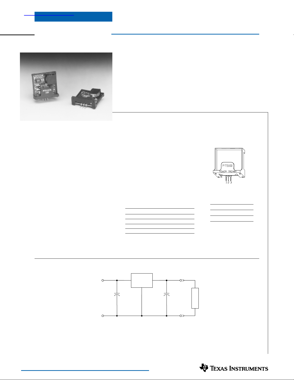
PT5100 Series
1-A Positive Step-down
Integrated Switching Regulator
Description
The PT5100 modules are a series of
economical, easy-to-use 1-A positive
step-down, Integrated Switching Regulators (ISRs). These ISRs are compatible
with most TO-220 style linear regulators,
and when employed as a linear replacement, provide significant benefits in
both efficiency and power dissipation.
They are recommended for use in a wide
variety of on-board power regulation
applications. These include computer,
data storage, industrial controls, and
battery powered equipment. Modules
are laser-trimmed for optimal output
voltage accuracy, and exhibit excellent
line and load regulation. The PT5100
also features output current limiting
and thermal shutdown protection.
Features
• 90%+ Efficiency
• Internal Short-Circuit Protection
• Pin-Compatible with 3-Terminal
Linear Regulators
• Laser-Trimmed Output Voltage
• Over-Temperature Protection
• Small Footprint
• Wide Input Range
• 5-Pin Mount Option
(Suffixes L & M)
Ordering Information
PT5101¨ = +5.0 Volts
PT5102¨ = +12.0 Volts
PT5103¨ = +3.3 Volts
PT5105¨ = +6.5 Volts
PT5107¨ = +15.0 Volts
PT5109¨ = +5.6 Volts
PT5110¨ = +9.0 Volts
PT5111¨ = +10.0 Volts
PT5112¨ = +8.0 Volts
PT Series Suffix
Case/Pin Order Package
Configuration Suffix Code
Vertical N (EAD)
Horizontal A (EAA)
SMD C (EAC)
Horizontal, 2-pin Tab M (EAM)
SMD, 2-Pin Tab L (EAL)
(Reference the applicable package code drawing for
the dimensions and PC board layout)
(PT1234x )
SLTS028B
(Revised 11/8/2001)
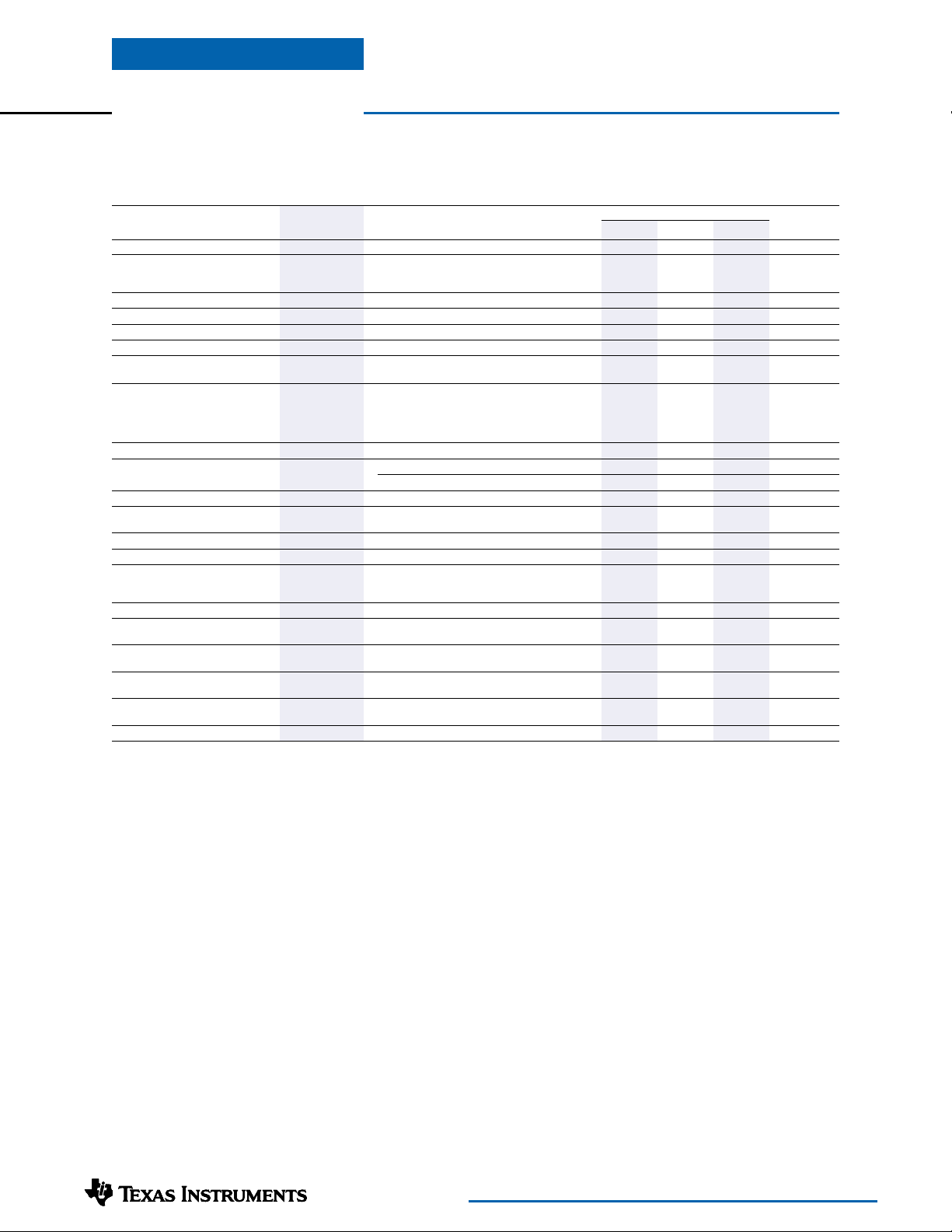
Package (EAD)
Pin-Out Information
Pin Function
1
2
3
V
in
GND
V
out
Standard Application
+V
IN
C
1
1µF
For technical support and more information, see inside back cover or visit www.ti.com
1
PT5100
2
3
C
2
100µF
+V
OUT
+
COMCOM
L
O
A
D
C1 = Optional 1µF ceramic capacitor
C2 = Required 100µF electrolytic
Page 2
PT5100 Series
1-A Positive Step-down
Integrated Switching Regulator
Specifications (Unless otherwise stated, T
=25°C, Vin =Vinmin, C
a
=100µF, and Io =Iomax)
out
PT5100 SERIES
Characteristic Symbol Conditions Min Typ Max Units
Output Current I
Input Voltage Range V
o
in
Over Vin range 0.1
Over Io Range V
=3.3V 9 — 26
o
=5.0V 9 — 38 VDC
V
o
V
>5.0V V
o
Set Point Voltage Tolerance Vo tol —±1±2%V
Temperature Variation Reg
Line Regulation Reg
Load Regulation Reg
Total Output Voltage Variation ∆V
temp
line
load
tot Includes set-point, line, load,
o
Efficiency η V
Vo Ripple (pk-pk) V
Transient Response t
Current Limit I
Switching Frequency ƒ
External Output Capacitance C
Operating Temperature Range T
Thermal Resistance θ
Storage Temperature T
∆V
r
tr
tr
lim
s
out
a
ja
s
Reliability MTBF Per Bellcore TR-332
Mechanical Shock — Per Mil-Std-883D, method 2002.3, — 500 — G’s
Mechanical Vibration — Per Mil-Std-883D, Method 2007.2 — 5
Weight — Suffixes N, A, & C — 4.5 —
0° ≤Ta ≤ +60°C, I
=Iomin — ±0.5 — %V
o
Over Vin range — ±5 ±10 mV
Over Io range — ±5 ±10 mV
0° ≤Ta ≤ +60°C
= 1 5V — 95 —
o
= 1 2V — 94 —
V
o
= 1 0V — 92 — %
V
o
=5.0V — 90 —
V
o
Vo =3.3V — 82 —
20MHz bandwidth — 2 — %V
1A/µs load step, 50% to 100% Iomax — 100 200 µs
Vo over/undershoot — ±5.0 — %V
∆V
= –1% 1.2 2.6 — A
o
Over Vin range V
≥ 5.0V 500 650 800
o
V
≤ 3.3V 575 725 875
o
Over Vin range –40
Free-air convection (40-60LFM) Vo =3.3V — 45 —
=5.0V — 50 — °C/W
V
o
V
≥ 12V — 60 —
o
— –40 — +125 °C
50% stress, Ta =40°C, ground benign
1mS, half-sine, mounted to a fixture
20-2000Hz, soldered in PC board
Suffixes L & M — 6.5 —
(1)
— 1.0 A
+ 4 — 38
o
— ±1.5 ±3 %V
kHz
100 — — µF
(2)
— +85
(3)
°C
11.3 — — 10
(4)
—G’s
grams
6
o
o
o
o
o
Hrs
Flammability — Materials meet UL 94V-0
Notes: (1) The ISR will operate at no load with reduced specifications.
(2) For operation below 0°C, use a tantalum type capacitor for C
(3) See Thermal Derating curves.
.
2
(4) The tab pins on the 5-pin mount package types (suffixes L & M) must be soldered. For more information see the applicable package outline drawing.
For technical support and more information, see inside back cover or visit www.ti.com
Page 3
PT5100 Series
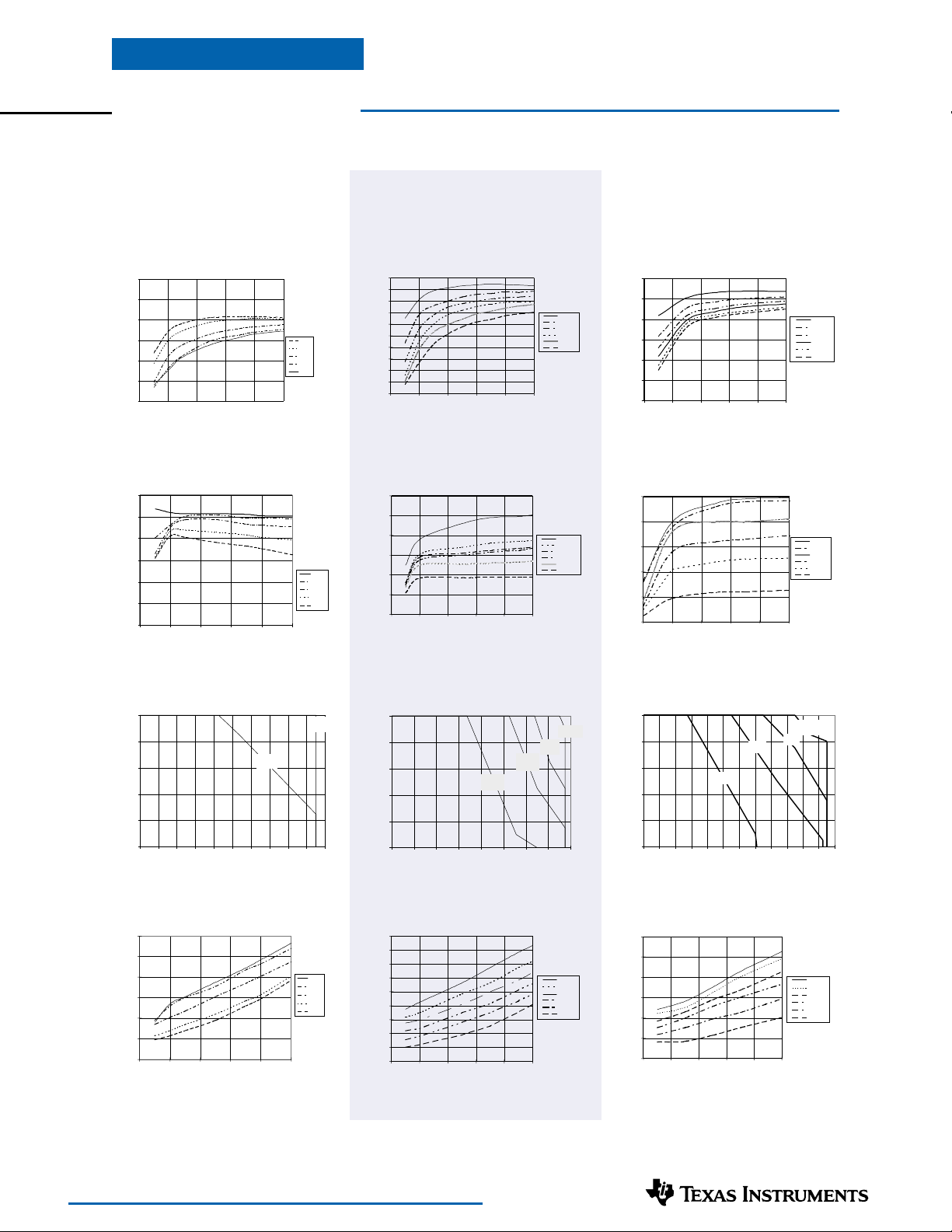
T ypical Characteristics
1-A Positive Step-down
Integrated Switching Regulator
PT5103, 3.3 VDC (See Note A) PT5101, 5.0 VDC (See Note A) PT5102, 12.0 VDC (See Note A)
Efficiency vs Output Current Efficiency vs Output Current
100
90
80
70
Efficiency - %Ripple-(mV)Iout-(Amps)PD-(Watts)
60
50
40
0 0.2 0.4 0.6 0.8 1
Iout-(Amps)
Vin
9.0V
12.0V
18.0V
24.0V
26.0V
90
85
80
75
70
65
60
Efficiency - %
55
50
45
40
0 0.2 0.4 0.6 0.8 1
Iout-(Amps)
Ripple vs Output Current Ripple vs Output Current
60
50
40
30
20
10
0
0 0.2 0.4 0.6 0.8 1
Iout-(Amps)
Vin
26.0V
24.0V
18.0V
12.0V
9.0V
120
100
80
60
40
Ripple-(mV)
20
0
0 0.2 0.4 0.6 0.8 1
Iout-(Amps)
Thermal Derating (Ta) (See Note B) Thermal Derating (Ta) (See Note B)
1
0.8
0.6
0.4
0.2
0
7 9 11 13 15 17 19 21 23 25 27
85°C
Vin-(Volts) Vin-(Volts)Vin-(Volts)
70°C
1
0.8
0.6
0.4
Iout-(Amps)
0.2
0
7 1115192327313539
85°C
70°C
60°C
Efficiency vs Output Current
100
Vin
9.0V
12.0V
18.0V
24.0V
30.0V
38.0V
90
80
70
Efficiency - %
60
50
40
0 0.2 0.4 0.6 0.8 1
Vin
16.0V
20.0V
24.0V
30.0V
35.0V
38.0V
Iout-(Amps)
Ripple vs Output Current
250
Vin
38.0V
30.0V
24.0V
18.0V
12.0V
9.0V
200
150
100
Ripple-(mV)Iout-(Amps)
50
0
0 0.2 0.4 0.6 0.8 1
Vin
38.0V
35.0V
30.0V
24.0V
20.0V
16.0V
Iout-(Amps)
Thermal Derating (Ta) (See Note B)
50°C
1
0.8
0.6
0.4
0.2
0
15 17 19 21 23 25 27 29 31 33 35 37 39
70°C
85°C
50°C
60°C
Power Dissipation vs Output Current Power Dissipation vs Output Current
1.2
1
0.8
0.6
0.4
0.2
0
0 0.2 0.4 0.6 0.8 1
Vin
26.0V
24.0V
18.0V
12.0V
9.0V
1.8
1.6
1.4
1.2
1
0.8
PD-(Watts)
0.6
0.4
0.2
0
0 0.2 0.4 0.6 0.8 1
Vin
38.0V
30.0V
24.0V
18.0V
12.0V
9.0V
Power Dissipation vs Output Current
2.4
2
1.6
1.2
PD-(Watts)
0.8
0.4
0
0 0.2 0.4 0.6 0.8 1
Iout-(Amps) Iout-(Amps) Iout-(Amps)
Note A: Characteristic data has been developed from actual products tested at 25°C. This data is considered typical data for the Converter.
Note B: Thermal derating graphs are developed in free-air convection cooling, which corresponds to approximately 40–60LFM of airflow.
For technical support and more information, see inside back cover or visit www.ti.com
Vin
38.0V
35.0V
30.0V
24.0V
20.0V
16.0V
Page 4

PACKAGE OPTION ADDENDUM
www.ti.com
PACKAGING INFORMATION
Orderable Device Status
PT5101A ACTIVE SIP MOD
PT5101C ACTIVE SIP MOD
PT5101CT ACTIVE SIP MOD
PT5101G ACTIVE SIP MOD
PT5101H ACTIVE SIP MOD
PT5101J ACTIVE SIP MOD
PT5101L ACTIVE SIP MOD
PT5101M ACTIVE SIP MOD
PT5101N ACTIVE SIP MOD
PT5101S ACTIVE SIP MOD
PT5101U ACTIVE SIP MOD
PT5102A ACTIVE SIP MOD
PT5102C ACTIVE SIP MOD
PT5102CT ACTIVE SIP MOD
PT5102H ACTIVE SIP MOD
PT5102J ACTIVE SIP MOD
PT5102M ACTIVE SIP MOD
PT5102N ACTIVE SIP MOD
PT5102S ACTIVE SIP MOD
PT5103A ACTIVE SIP MOD
PT5103C ACTIVE SIP MOD
PT5103H ACTIVE SIP MOD
PT5103J ACTIVE SIP MOD
PT5103L ACTIVE SIP MOD
PT5103M ACTIVE SIP MOD
(1)
Package
Type
ULE
ULE
ULE
ULE
ULE
ULE
ULE
ULE
ULE
ULE
ULE
ULE
ULE
ULE
ULE
ULE
ULE
ULE
ULE
ULE
ULE
ULE
ULE
ULE
ULE
13-Oct-2005
Package
Drawing
EAA 3 35 TBD Call TI Level-1-215C-UNLIM
EAC 3 35 TBD Call TI Level-1-215C-UNLIM
EAC 3 200 TBD Call TI Level-1-215C-UNLIM
EAG 3 16 TBD Call TI Level-1-215C-UNLIM
EAH 3 16 TBD Call TI Level-1-215C-UNLIM
EAJ 3 16 TBD Call TI Level-1-215C-UNLIM
EAL 3 35 TBD Call TI Level-1-215C-UNLIM
EAM 3 35 TBD Call TI Level-1-215C-UNLIM
EAD 3 35 TBD Call TI Level-1-215C-UNLIM
EAF 3 16 TBD Call TI Level-1-215C-UNLIM
EAU 3 35 TBD Call TI Level-1-215C-UNLIM
EAA 3 35 TBD Call TI Level-1-215C-UNLIM
EAC 3 35 TBD Call TI Level-1-215C-UNLIM
EAC 3 200 TBD Call TI Level-1-215C-UNLIM
EAH 3 16 TBD Call TI Level-1-215C-UNLIM
EAJ 3 16 TBD Call TI Level-1-215C-UNLIM
EAM 3 35 TBD Call TI Level-1-215C-UNLIM
EAD 3 35 TBD Call TI Level-1-215C-UNLIM
EAF 3 16 TBD Call TI Level-1-215C-UNLIM
EAA 3 35 TBD Call TI Level-1-215C-UNLIM
EAC 3 35 TBD Call TI Level-1-215C-UNLIM
EAH 3 16 TBD Call TI Level-1-215C-UNLIM
EAJ 3 16 TBD Call TI Level-1-215C-UNLIM
EAL 3 35 TBD Call TI Level-1-215C-UNLIM
EAM 3 35 TBD Call TI Level-1-215C-UNLIM
Pins Package
Qty
Eco Plan
(2)
Lead/Ball Finish MSL Peak Temp
(3)
Addendum-Page 1
Page 5
PACKAGE OPTION ADDENDUM
www.ti.com
Orderable Device Status
(1)
PT5103N ACTIVE SIP MOD
PT5105A ACTIVE SIP MOD
PT5105C ACTIVE SIP MOD
PT5105L ACTIVE SIP MOD
PT5105N ACTIVE SIP MOD
PT5107A ACTIVE SIP MOD
PT5107C ACTIVE SIP MOD
PT5107J ACTIVE SIP MOD
PT5107M ACTIVE SIP MOD
PT5107N ACTIVE SIP MOD
PT5109A ACTIVE SIP MOD
PT5109C ACTIVE SIP MOD
PT5109M ACTIVE SIP MOD
PT5109N ACTIVE SIP MOD
PT5110A ACTIVE SIP MOD
PT5110C ACTIVE SIP MOD
PT5110N ACTIVE SIP MOD
PT5110S ACTIVE SIP MOD
PT5111A ACTIVE SIP MOD
PT5111C ACTIVE SIP MOD
PT5111M ACTIVE SIP MOD
PT5111N ACTIVE SIP MOD
PT5112A ACTIVE SIP MOD
PT5112C ACTIVE SIP MOD
PT5112L ACTIVE SIP MOD
PT5112N ACTIVE SIP MOD
Package
Type
ULE
ULE
ULE
ULE
ULE
ULE
ULE
ULE
ULE
ULE
ULE
ULE
ULE
ULE
ULE
ULE
ULE
ULE
ULE
ULE
ULE
ULE
ULE
ULE
ULE
ULE
13-Oct-2005
Package
Drawing
Pins Package
Qty
Eco Plan
(2)
Lead/Ball Finish MSL Peak Temp
EAD 3 35 TBD Call TI Level-1-215C-UNLIM
EAA 3 35 TBD Call TI Level-1-215C-UNLIM
EAC 3 35 TBD Call TI Level-1-215C-UNLIM
EAL 3 35 TBD Call TI Level-1-215C-UNLIM
EAD 3 35 TBD Call TI Level-1-215C-UNLIM
EAA 3 35 TBD Call TI Level-1-215C-UNLIM
EAC 3 35 TBD Call TI Level-1-215C-UNLIM
EAJ 3 16 TBD Call TI Level-1-215C-UNLIM
EAM 3 35 TBD Call TI Level-1-215C-UNLIM
EAD 3 35 TBD Call TI Level-1-215C-UNLIM
EAA 3 35 TBD Call TI Level-1-215C-UNLIM
EAC 3 35 TBD Call TI Level-1-215C-UNLIM
EAM 3 35 TBD Call TI Level-1-215C-UNLIM
EAD 3 35 TBD Call TI Level-1-215C-UNLIM
EAA 3 35 TBD Call TI Level-1-215C-UNLIM
EAC 3 35 TBD Call TI Level-1-215C-UNLIM
EAD 3 35 TBD Call TI Level-1-215C-UNLIM
EAF 3 16 TBD Call TI Level-1-215C-UNLIM
EAA 3 35 TBD Call TI Level-1-215C-UNLIM
EAC 3 35 TBD Call TI Level-1-215C-UNLIM
EAM 3 35 TBD Call TI Level-1-215C-UNLIM
EAD 3 35 TBD Call TI Level-1-215C-UNLIM
EAA 3 35 TBD Call TI Level-1-215C-UNLIM
EAC 3 35 TBD Call TI Level-1-215C-UNLIM
EAL 3 35 TBD Call TI Level-1-215C-UNLIM
EAD 3 35 TBD Call TI Level-1-215C-UNLIM
(3)
Addendum-Page 2
Page 6

PACKAGE OPTION ADDENDUM
www.ti.com
(1)
The marketing status values are defined as follows:
13-Oct-2005
ACTIVE: Product device recommended for new designs.
LIFEBUY: TI has announced that the device will be discontinued, and a lifetime-buy period is in effect.
NRND: Not recommended for new designs. Device is in production to support existing customers, but TI does not recommend using this part in
a new design.
PREVIEW: Device has been announced but is not in production. Samples may or may not be available.
OBSOLETE: TI has discontinued the production of the device.
(2)
Eco Plan - The planned eco-friendly classification: Pb-Free (RoHS) or Green (RoHS & no Sb/Br) - please check
http://www.ti.com/productcontent for the latest availability information and additional product content details.
TBD: The Pb-Free/Green conversion plan has not been defined.
Pb-Free (RoHS): TI's terms "Lead-Free" or "Pb-Free" mean semiconductor products that are compatible with the current RoHS requirements
for all 6 substances, including the requirement that lead not exceed 0.1% by weight in homogeneous materials. Where designed to be soldered
at high temperatures, TI Pb-Free products are suitable for use in specified lead-free processes.
Green (RoHS & no Sb/Br): TI defines "Green" to mean Pb-Free (RoHS compatible), and free of Bromine (Br) and Antimony (Sb) based flame
retardants (Br or Sb do not exceed 0.1% by weight in homogeneous material)
(3)
MSL, Peak Temp. -- The Moisture Sensitivity Level rating according to the JEDEC industry standard classifications, and peak solder
temperature.
Important Information and Disclaimer:The information provided on this page represents TI's knowledge and belief as of the date that it is
provided. TI bases its knowledge and belief on information provided by third parties, and makes no representation or warranty as to the
accuracy of such information. Efforts are underway to better integrate information from third parties. TI has taken and continues to take
reasonable steps to provide representative and accurate information but may not have conducted destructive testing or chemical analysis on
incoming materials and chemicals. TI and TI suppliers consider certain information to be proprietary, and thus CAS numbers and other limited
information may not be available for release.
In no event shall TI's liability arising out of such information exceed the total purchase price of the TI part(s) at issue in this document sold by TI
to Customer on an annual basis.
Addendum-Page 3
Page 7

IMPORTANT NOTICE
Texas Instruments Incorporated and its subsidiaries (TI) reserve the right to make corrections, modifications,
enhancements, improvements, and other changes to its products and services at any time and to discontinue
any product or service without notice. Customers should obtain the latest relevant information before placing
orders and should verify that such information is current and complete. All products are sold subject to TI’s terms
and conditions of sale supplied at the time of order acknowledgment.
TI warrants performance of its hardware products to the specifications applicable at the time of sale in
accordance with TI’s standard warranty. Testing and other quality control techniques are used to the extent TI
deems necessary to support this warranty . Except where mandated by government requirements, testing of all
parameters of each product is not necessarily performed.
TI assumes no liability for applications assistance or customer product design. Customers are responsible for
their products and applications using TI components. To minimize the risks associated with customer products
and applications, customers should provide adequate design and operating safeguards.
TI does not warrant or represent that any license, either express or implied, is granted under any TI patent right,
copyright, mask work right, or other TI intellectual property right relating to any combination, machine, or process
in which TI products or services are used. Information published by TI regarding third-party products or services
does not constitute a license from TI to use such products or services or a warranty or endorsement thereof.
Use of such information may require a license from a third party under the patents or other intellectual property
of the third party, or a license from TI under the patents or other intellectual property of TI.
Reproduction of information in TI data books or data sheets is permissible only if reproduction is without
alteration and is accompanied by all associated warranties, conditions, limitations, and notices. Reproduction
of this information with alteration is an unfair and deceptive business practice. TI is not responsible or liable for
such altered documentation.
Resale of TI products or services with statements different from or beyond the parameters stated by TI for that
product or service voids all express and any implied warranties for the associated TI product or service and
is an unfair and deceptive business practice. TI is not responsible or liable for any such statements.
Following are URLs where you can obtain information on other Texas Instruments products and application
solutions:
Products Applications
Amplifiers amplifier.ti.com Audio www.ti.com/audio
Data Converters dataconverter.ti.com Automotive www.ti.com/automotive
DSP dsp.ti.com Broadband www.ti.com/broadband
Interface interface.ti.com Digital Control www.ti.com/digitalcontrol
Logic logic.ti.com Military www.ti.com/military
Power Mgmt power.ti.com Optical Networking www.ti.com/opticalnetwork
Microcontrollers microcontroller.ti.com Security www.ti.com/security
Telephony www.ti.com/telephony
Video & Imaging www.ti.com/video
Wireless www.ti.com/wireless
Mailing Address: Texas Instruments
Post Office Box 655303 Dallas, Texas 75265
Copyright 2005, Texas Instruments Incorporated
Page 8

Copyright © Each Manufacturing Company.
All Datasheets cannot be modified without permission.
This datasheet has been download from :
www.AllDataSheet.com
100% Free DataSheet Search Site.
Free Download.
No Register.
Fast Search System.
www.AllDataSheet.com
 Loading...