

Page 1

Product
Folder
Sample &
Buy
Technical
Documents
Tools &
Software
Support &
Community
CC3200MOD
SWRS166 –DECEMBER 2014
CC3200MOD SimpleLink™ Wi-Fi®and Internet-of-Things Module Solution, a Single-Chip
Wireless MCU
1 Module Overview
1.1 Features
1
• The CC3200MOD is a Wi-Fi Module that Consists
of the CC3200R1M2RGC Single-Chip Wireless
MCU. This Fully Integrated Module Includes all
Required Clocks, SPI Flash, and Passives.
• Modular FCC, IC, and CE Certifications Save
Customer Effort, Time, and Money
• Wi-Fi CERTIFIED™ Modules, With Ability to
Request Certificate Transfer for Wi-Fi Alliance
Members
• 1.27-mm Pitch LGA Package for Easy Assembly
and Low-Cost PCB Design
• Applications Microcontroller Subsystem
– ARM Cortex-M4 Core at 80 MHz
– Embedded Memory Options
• Integrated Serial
• RAM (up to 256KB)
• Peripheral Drivers in ROM
– Hardware Crypto Engine for Advanced
Hardware Security Including
• AES, DES, and 3DES
• SHA and MD5
• CRC and Checksum
– 8-Bit, Fast, Parallel Camera Interface
– 1 Multichannel Audio Serial Port (McASP)
Interface With Support for I2S Format
– 1 SD (MMC) Interface
– 32-Channel Micro Direct Memory Access
(μDMA)
– 2 Universal Asynchronous
Receivers/Transmitters (UARTs)
– 2 Serial Peripheral Interfaces (SPIs)
– 1 Inter-integrated Circuit (I2C)
– 4 General-Purpose Timers (GPTs)
– 16-Bit Pulse-Width Modulation (PWM) Mode
– 1 Watchdog Timer Module
– 4-Channel 12-Bit Analog-to-Digital Converters
(ADCs)
– Up to 25 Individually Programmable GPIO Pins
• Wi-Fi Network Processor Subsystem
– 802.11b/g/n Radio, Baseband, and Medium
Access Control
– TCP/IP Stack
• 8 Simultaneous TCP, UDP, or RAW Sockets
• 2 Simultaneous TLS v1.2 or SSL 3.0
Sockets
– Powerful Crypto Engine for Fast, Secured
WLAN Connections With 256-Bit Encryption
– Station, Access Point, and Wi-Fi Direct™ Modes
– WPA2 Personal and Enterprise Security
– SimpleLink Connection Manager for Managing
Wi-Fi Security States
– TX Power
• 17 dBm at 1 DSSS
• 17.25 dBm at 11 CCK
• 13.5 dBm at 54 OFDM
– RX Sensitivity
• –94.7 dBm at 1 DSSS
• –87 dBm at 11 CCK
• –73 dBm at 54 OFDM
– Application Throughput
• UDP: 16 Mbps
• TCP: 13 Mbps
• Power-Management Subsystem
– Integrated DC-DC Converter With a Wide-
Supply Voltage:
• VBAT: 2.3 to 3.6 V
– Low-Power Consumption at 3.6 V
• Hibernate With Real-Time Clock (RTC):
7 μA
• Low-Power Deep Sleep: <275 μA
• RX Traffic: 59 mA at 54 OFDM
• TX Traffic: 229 mA at 54 OFDM
– Additional Integrated Components
• 40.0-MHz Crystal
• 32.768-kHz Crystal (RTC)
• 8-Mbit SPI Serial Flash RF Filter and
Passive Components
– Package and Operating Conditions
• 1.27-mm Pitch, 63-Pin, 20.5-mm ×
17.5 mm LGA Package for Easy Assembly
and Low-Cost PCB Design
• Operating Temperature Range: –20°C to
70°C
1
An IMPORTANT NOTICE at the end of this data sheet addresses availability, warranty, changes, use in safety-critical applications,
intellectual property matters and other important disclaimers. PRODUCTION DATA.
Page 2

CC3200MOD
SWRS166 –DECEMBER 2014
1.2 Applications
• Internet of Things (IoT) • Internet Gateway
• Cloud Connectivity • Industrial Control
• Home Automation • Smart Plug and Metering
• Home Appliances • Wireless Audio
• Access Control • IP Network Sensor Nodes
• Security Systems • Wearables
• Smart Energy
1.3 Description
Start your design with the industry’s first programmable FCC, IC, CE, and Wi-Fi Certified Wireless
microcontroller (MCU) module with built-in Wi-Fi connectivity. Created for the Internet of Things (IoT), the
SimpleLink CC3200MOD is a wireless MCU module that integrates an ARM Cortex-M4 MCU, allowing
customers to develop an entire application with a single device. With on-chip Wi-Fi, Internet, and robust
security protocols, no prior Wi-Fi experience is required for faster development. The CC3200MOD
integrates all required system-level hardware components including clocks, SPI flash, RF switch, and
passives into an LGA package for easy assembly and low-cost PCB design. The CC3200MOD is provided
as a complete platform solution including software, sample applications, tools, user and programming
guides, reference designs, and the TI E2E™ support community
www.ti.com
The applications MCU subsystem contains an industry-standard ARM Cortex-M4 core running at 80 MHz.
The device includes a wide variety of peripherals, including a fast parallel camera interface, I2S, SD/MMC,
UART, SPI, I2C, and four-channel ADC. The CC3200 family includes flexible embedded RAM for code
and data; ROM with external serial flash bootloader and peripheral drivers; and SPI flash for Wi-Fi network
processor service packs, Wi-Fi certificates, and credentials.
The Wi-Fi network processor subsystem features a Wi-Fi Internet-on-a-chip™ and contains an additional
dedicated ARM MCU that completely off-loads the applications MCU. This subsystem includes an 802.11
b/g/n radio, baseband, and MAC with a powerful crypto engine for fast, secure Internet connections with
256-bit encryption. The CC3200MOD supports station, access point, and Wi-Fi Direct™ modes. The
device also supports WPA2 personal and enterprise security and WPS 2.0. The Wi-Fi Internet-on-a-chip
includes embedded TCP/IP and TLS/SSL stacks, HTTP server, and multiple Internet protocols. The
power-management subsystem includes integrated DC-DC converters supporting a wide range of supply
voltages. This subsystem enables low-power consumption modes, such as the hibernate with RTC mode
requiring less than 7 μA of current.
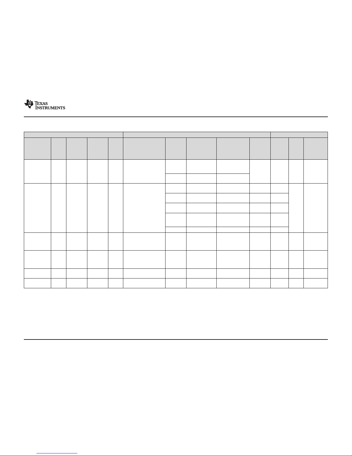
Table 1-1. Module Information
PART NUMBER PACKAGE BODY SIZE
CC3200MODR1M2AMOB MOB (63) 20.5 mm × 17.5 mm
(1) For more information, see Section 9, Mechanical Packaging and Orderable Information.
(1)
2 Module Overview Copyright © 2014, Texas Instruments Incorporated
Submit Documentation Feedback
Page 3
CC3200MOD
V
CC
GPIO &
Peripheral
Interfaces
RF Filter
Serial
Flash
8Mbit
Pull-up
resistors
CC3200R1M2RGC
Power
Inductors
Caps
32-KHz
Crystal
40-MHz
Crystal
www.ti.com
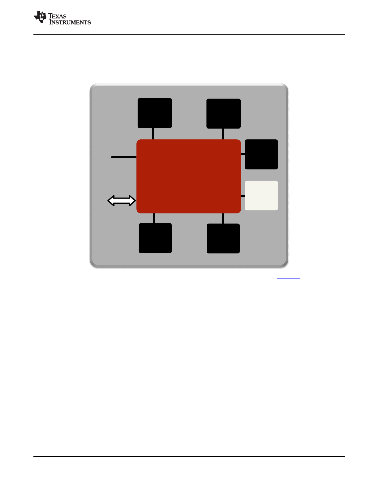
1.4 Functional Block Diagram
Figure 1-1 shows the functional block diagram of the CC3200MOD module.
CC3200MOD
SWRS166 –DECEMBER 2014
(1) For 3200MOD module pin multiplexing details, refer to CC3200R device datasheet (literature number: SWAS032)
Figure 1-1. CC3200MOD Module Functional Block Diagram
Copyright © 2014, Texas Instruments Incorporated Module Overview 3
Submit Documentation Feedback
Page 4
ARM Cortex-M4 80 MHz Processor
ARM Processor (Wi-Fi Network Processor)
Wi-Fi Baseband
Wi-Fi MAC
Wi-Fi Radio
Wi-Fi Driver
Supplicant
TCP/IP
TLS/SSL
Internet Protocols
User Application
Embedded Wi-Fi
Embedded Internet
CC3200MOD
SWRS166 –DECEMBER 2014
www.ti.com
Figure 1-2. CC3200 Hardware Overview
4 Module Overview Copyright © 2014, Texas Instruments Incorporated
Figure 1-3. CC3200 Software Overview
Submit Documentation Feedback
Page 5

CC3200MOD
www.ti.com
SWRS166 –DECEMBER 2014
Table of Contents
1 Module Overview ........................................ 1 5.3 ARM Cortex-M4 Processor Core Subsystem ....... 42
1.1 Features .............................................. 1 5.4 CC3200 Device Encryption ......................... 43
1.2 Applications........................................... 2 5.5 Wi-Fi Network Processor Subsystem ............... 44
1.3 Description............................................ 2 5.6 Power-Management Subsystem .................... 45
1.4 Functional Block Diagram ............................ 3 5.7 Low-Power Operating Mode ........................ 45
2 Revision History ......................................... 6 5.8 Memory.............................................. 46
3 Terminal Configuration and Functions.............. 7 5.9 Boot Modes.......................................... 48
3.1 CC3200MOD Pin Diagram ........................... 7 6 Applications, Implementation, and Layout ....... 51
3.2 Pin Attributes ......................................... 8 6.1 Reference Schematics.............................. 51
3.3 Pin Attributes and Pin Multiplexing.................. 10 6.2 Bill of Materials...................................... 52
3.4 Recommended Pin Multiplexing Configurations .... 19 6.3 Layout Recommendations .......................... 52
3.5 Drive Strength and Reset States for Analog-Digital
Multiplexed Pins..................................... 22
3.6 Pad State After Application of Power To Chip But
Prior To Reset Release ............................. 22
4 Specifications........................................... 23
4.1 Absolute Maximum Ratings......................... 23
4.2 Handling Ratings .................................... 23
4.3 Power-On Hours .................................... 23
4.4 Recommended Operating Conditions............... 23
4.5 Brown-Out and Black-Out........................... 24
4.6 Electrical Characteristics (3.3 V, 25°C) ............. 25
4.7 Thermal Resistance Characteristics for MOB
Package ............................................. 26
4.8 Reset Requirement ................................. 26
4.9 Current Consumption ............................... 27
4.10 WLAN RF Characteristics........................... 30
4.11 Timing Characteristics............................... 31
5 Detailed Description ................................... 42
5.1 Overview ............................................ 42
5.2 Functional Block Diagram........................... 42
7 Environmental Requirements and
Specifications........................................... 56
7.1 Temperature......................................... 56
7.2 Handling Environment .............................. 56
7.3 Storage Condition ................................... 56
7.4 Baking Conditions................................... 56
7.5 Soldering and Reflow Condition .................... 56
8 Product and Documentation Support.............. 58
8.1 Development Support ............................... 58
8.2 Device Nomenclature ............................... 58
8.3 Community Resources .............................. 59
8.4 Trademarks.......................................... 59
8.5 Electrostatic Discharge Caution..................... 59
8.6 Export Control Notice ............................... 59
8.7 Glossary............................................. 59
9 Mechanical Packaging and Orderable
Information .............................................. 60
9.1 Mechanical Drawing................................. 60
9.2 Package Option ..................................... 61
Copyright © 2014, Texas Instruments Incorporated Table of Contents 5
Submit Documentation Feedback
Page 6

CC3200MOD
SWRS166 –DECEMBER 2014
2 Revision History
DATE REVISION NOTES
November 2014 * Initial release.
www.ti.com
6 Revision History Copyright © 2014, Texas Instruments Incorporated
Submit Documentation Feedback
Page 7
44
45
46
47
48
49
50
51
52
53
54
27
26
25
24
23
22
21
20
19
18
17
28 29 30 31 3332 34 35 36 37 38 39 40 41 42 43
16 15 14 13 1112 10 9 8 7 6 5 4 3 2 1
63
59
55
62 61
60
57 56
58
GND
ANTSEL2
ANTSEL1
SOP1
SOP2
JTAG_TMS
JTAG_TCK
NC
GPIO28
JTAG_TDO
NC
GND
NC
NC
NC
GPIO22
GPIO13
GPIO12
GPIO17
GPIO16
GPIO15
GPIO14
GPIO11
GPIO10
GND
GND
GPIO0
NC
GPIO1
GPIO2
GPIO3
GPIO4
GPIO5
GPIO6
GPIO7
GPIO8
GPIO9
GND
NC
GND
RF
_
BG
GND
NC
SOP
0
nRESET
VBAT
_
DCDC
_
ANA
VBAT
_
DCDC
_
PA
GND
VDD
_
ANA
2
VBAT
_
DCDC
_
DIG
_
IO
NC
GPIO30
GND
GND
GND
GND
GND
GND
GND
GND
GND
CC3200MOD
www.ti.com
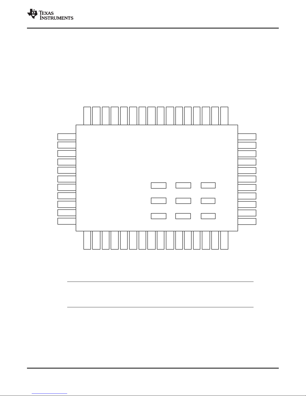
3 Terminal Configuration and Functions
3.1 CC3200MOD Pin Diagram
Figure 3-1 shows the pin diagram for the CC3200MOD.
CC3200MOD
SWRS166 –DECEMBER 2014
NOTE
Figure 3-1 shows the approximate location of pins on the module. For the actual mechanical
diagram refer to Section 9.
Figure 3-1. CC3200MOD Pin Diagram (Bottom View)
Copyright © 2014, Texas Instruments Incorporated Terminal Configuration and Functions 7
Submit Documentation Feedback
Page 8
CC3200MOD
SWRS166 –DECEMBER 2014
www.ti.com
3.2 Pin Attributes
Table 3-1 lists the pin descriptions of the CC3200MOD module. "DEVICE PIN NO" refers to the pin
number of the QFN part CC3200. This is stated here because the QFN pin is referred to in the SDK.
Table 3-1. Pin Attributes
MODULE MODULE PIN NAME TYPE DEVICE PIN NO MODULE PIN DESCRIPTION
PIN NO.
1 GND - Ground
2 GND - Ground
3 GPIO10 I/O 1 GPIO
4 GPIO11 I/O 2 GPIO
5 GPIO14 I/O 5 GPIO
6 GPIO15 I/O 6 GPIO
7 GPIO16 I/O 7 GPIO
8 GPIO17 I/O 8 GPIO
9 GPIO12 I/O 3 GPIO
10 GPIO13 I/O 4 GPIO
11 GPIO22 I/O 15 GPIO
12 JTAG_TDI I/O 16 GPIO
13 NC - 13 Reserved for TI
14 NC - 14 Reserved for TI
15 NC - 11 Reserved for TI
16 GND - Ground
17 NC - 12 Reserved for TI
18 JTAG_TDO I/O 17 GPIO
19 GPIO28 I/O 18 GPIO
20 NC - 23 Unused. Do not connect.
21 JTAG_TCK I/O 19 JTAG TCK input. Needs 100-kΩ pulldown resistor to ground.
22 JTAG_TMS I/O 20 JTAG TMS input. Leave unconnected if not used on product.
23 SOP2 - 21 Add 2.7-kΩ pulldown resistor to ground needed for functional
24 SOP1 - 34 Reserved. Do not connect.
25 ANTSEL1 I/O 29 Antenna selection control
26 ANTSEL2 I/O 30 Antenna selection control
27 GND - Ground
28 GND - Ground
29 NC - 27, 28 Reserved for TI
30 GND - Ground
31 RF_BG I/O 31 2.4-GHz RF input/output
32 GND - Ground
33 NC - 38 Reserved for TI
34 SOP0 - 35 Optional 10-kΩ pullup if user chooses to use SWD debug mode
35 nRESET I 32 Power on reset. Does not require external RC circuit
36 VBAT_DCDC_ANA - 37 Power supply for the device, can be connected to battery (2.3 V
37 VBAT_DCDC_PA - 39 Power supply for the device, can be connected to battery (2.3 V
38 GND - Ground
(1)
(1)
(1)
(1)
(1)
(1)
(1)
(1)
(1)
(1)
(1)
(1)
mode. Add option to pullup required for entering the UART load
mode for flashing.
(1)
(1)
instead of 4-wire JTAG
to 3.6 V)
to 3.6 V)
(1)
(1)
(1) For pin multiplexing details, refer to CC3200R device data sheet
8 Terminal Configuration and Functions Copyright © 2014, Texas Instruments Incorporated
Submit Documentation Feedback
Page 9
CC3200MOD
www.ti.com
SWRS166 –DECEMBER 2014
Table 3-1. Pin Attributes (continued)
MODULE MODULE PIN NAME TYPE DEVICE PIN NO MODULE PIN DESCRIPTION
PIN NO.
39 NC - 47 Leave unconnected
40 VBAT_DCDC_DIG_IO - 10, 44, 54 Power supply for the device, can be connected to battery (2.3 V
41 NC - 25, 36, 48 Reserved for TI
42 GPIO30 I/O 53 GPIO
43 GND - Ground
44 GPIO0 I/O 50 GPIO
45 NC - 51 Reserved for TI
46 GPIO1 I/O 55 GPIO
47 GPIO2 I/O 57 GPIO
48 GPIO3 I/O 58 GPIO
49 GPIO4 I/O 59 GPIO
50 GPIO5 I/O 60 GPIO
51 GPIO6 I/O 61 GPIO
52 GPIO7 I/O 62 GPIO
53 GPIO8 I/O 63 GPIO
54 GPIO9 I/O 64 GPIO
55 GND - Thermal Ground
56 GND - Thermal Ground
57 GND - Thermal Ground
58 GND - Thermal Ground
59 GND - Thermal Ground
60 GND - Thermal Ground
61 GND - Thermal Ground
62 GND - Thermal Ground
63 GND - Thermal Ground
to 3.6 V)
(1)
(1)
(1)
(1)
(1)
(1)
(1)
(1)
(1)
(1)
(1)
Copyright © 2014, Texas Instruments Incorporated Terminal Configuration and Functions 9
Submit Documentation Feedback
Page 10

CC3200MOD
SWRS166 –DECEMBER 2014
3.3 Pin Attributes and Pin Multiplexing
The module makes extensive use of pin multiplexing to accommodate the large number of peripheral
functions in the smallest possible package. To achieve this configuration, pin multiplexing is controlled
using a combination of hardware configuration (at module reset) and register control.
The board and software designers are responsible for the proper pin multiplexing configuration. Hardware
does not ensure that the proper pin multiplexing options are selected for the peripherals or interface mode
used. Table 3-2 describes the general pin attributes and presents an overview of pin multiplexing. All pin
multiplexing options are configurable using the pin mux registers. The following special considerations
apply:
• All I/Os support drive strengths of 2, 4, and 6 mA. Drive strength is configurable individually for each
pin.
• All I/Os support 10-μA pullups and pulldowns.
• These pulls are not active and all of the I/Os remain floating while the device is in Hibernate state.
• The VIO and VBAT supply must be tied together at all times.
• All digital I/Os are nonfail-safe.
If an external device drives a positive voltage to the signal pads and the CC3200MOD is not
powered, DC current is drawn from the other device. If the drive strength of the external
device is adequate, an unintentional wakeup and boot of the CC3200MOD can occur. To
prevent current draw, TI recommends any one of the following:
• All devices interfaced to the CC3200MOD must be powered from the same power rail as
the chip.
• Use level-shifters between the module and any external devices fed from other
independent rails.
• The nRESET pin of the CC3200MOD must be held low until the VBAT supply to the
module is driven and stable
www.ti.com
NOTE
10 Terminal Configuration and Functions Copyright © 2014, Texas Instruments Incorporated
Submit Documentation Feedback
Page 11
CC3200MOD
www.ti.com
SWRS166 –DECEMBER 2014
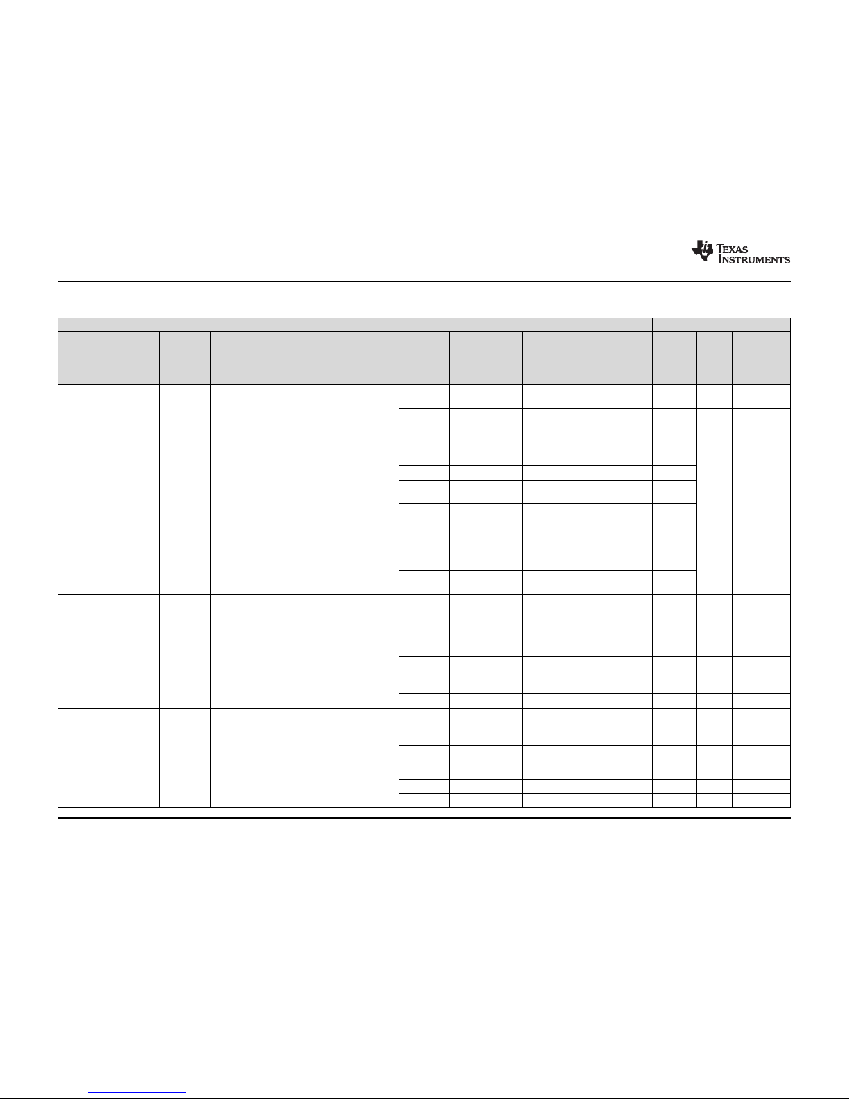
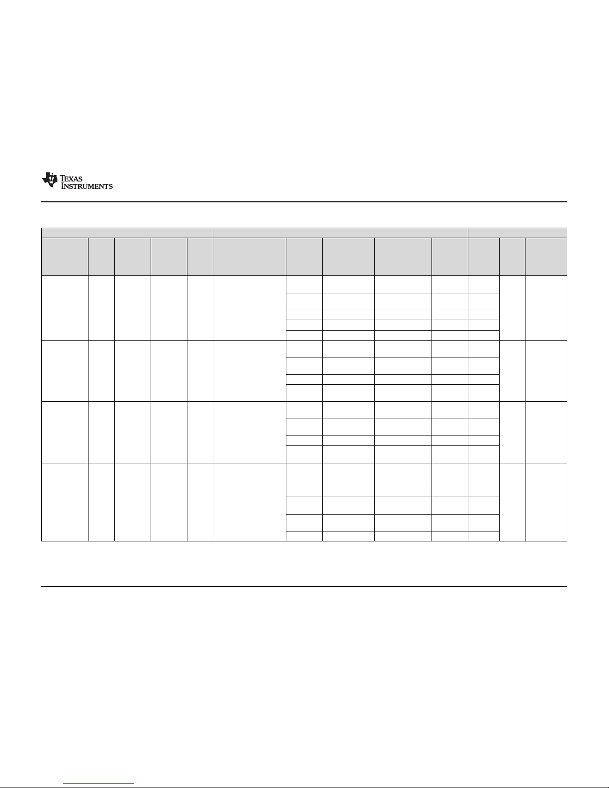
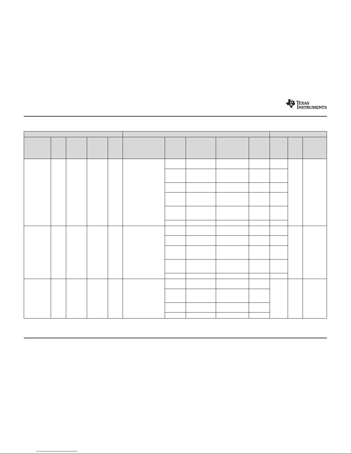
Table 3-2. Pin Multiplexing
General Pin Attributes Function Pad States
Pin Alias Use Select as Config Muxed Dig. Pin Mux Config Dig. Pin Signal Name Signal Signal LPDS
(1)
Hib
(2)
nRESET = 0
Wakeup Addl with Reg Mux Description Direction
Source Analog JTAG Config
Mux Mode
Value
General-Purpose
0 GPIO10 I/O Hi-Z
I/O
1 I2C_SCL I2C Clock O Hi-Z
(Open
Drain)
GPIO_PAD_CONFIG_1
GPIO10 I/O No No No 0 Hi-Z Hi-Z
3 GT_PWM06 Pulse-Width O Hi-Z
(0x4402 E0C8)
Modulated O/P
7 UART1_TX UART TX Data O 1
6 SDCARD_CLK SD Card Clock O 0
12 GT_CCP01 Timer Capture Port I Hi-Z
General-Purpose
0 GPIO11 I/O Hi-Z
I/O
1 I2C_SDA I2C Data I/O Hi-Z
(Open
Drain)
3 GT_PWM07 Pulse-Width O Hi-Z
Modulated O/P
GPIO_PAD_CONFIG_1
4 pXCLK (XVCLK) Free Clock To O 0
GPIO11 I/O Yes No No 1 Hi-Z Hi-Z
Parallel Camera
(0x4402 E0CC)
6 SDCARD_CMD SD Card I/O Hi-Z
Command Line
7 UART1_RX UART RX Data I Hi-Z
12 GT_CCP02 Timer Capture Port I Hi-Z
13 McAFSX I2S Audio Port O Hi-Z
Frame Sync
Copyright © 2014, Texas Instruments Incorporated Terminal Configuration and Functions 11
Submit Documentation Feedback
Page 12
CC3200MOD
SWRS166 –DECEMBER 2014
www.ti.com
Table 3-2. Pin Multiplexing (continued)
General Pin Attributes Function Pad States
Pin Alias Use Select as Config Muxed Dig. Pin Mux Config Dig. Pin Signal Name Signal Signal LPDS
(1)
Hib
(2)
nRESET = 0
Wakeup Addl with Reg Mux Description Direction
Source Analog JTAG Config
Mux Mode
Value
General Purpose
0 GPIO12 I/O Hi-Z
I/O
3 McACLK I2S Audio Port O Hi-Z
Clock O
4 pVS (VSYNC) Parallel Camera I Hi-Z
GPIO_PAD_CONFIG_1
Vertical Sync
GPIO12 I/O No No No 2 Hi-Z Hi-Z
(0x4402 E0D0)
5 I2C_SCL I2C Clock I/O Hi-Z
(Open
Drain)
7 UART0_TX UART0 TX Data O 1
12 GT_CCP03 Timer Capture Port I Hi-Z
General-Purpose
0 GPIO13 I/O
I/O
5 I2C_SDA I2C Data I/O
(Open
GPIO_PAD_CONFIG_1
Drain)
GPIO13 I/O Yes No No 3 Hi-Z Hi-Z Hi-Z
(0x4402 E0D4) 4 pHS (HSYNC) Parallel Camera I
Horizontal Sync
7 UART0_RX UART0 RX Data I
12 GT_CCP04 Timer Capture Port I
General-Purpose
0 GPIO14 I/O
I/O
5 I2C_SCL I2C Clock I/O
(Open
GPIO_PAD_CONFIG_1
Drain)
GPIO14 I/O No No 4 Hi-Z Hi-Z Hi-Z
(0x4402 E0D8) 7 GSPI_CLK General SPI Clock I/O
4 pDATA8 Parallel Camera I
(CAM_D4) Data Bit 4
12 GT_CCP05 Timer Capture Port I
12 Terminal Configuration and Functions Copyright© 2014, Texas Instruments Incorporated
Submit Documentation Feedback
Page 13
CC3200MOD
www.ti.com
SWRS166 –DECEMBER 2014
Table 3-2. Pin Multiplexing (continued)
General Pin Attributes Function Pad States
Pin Alias Use Select as Config Muxed Dig. Pin Mux Config Dig. Pin Signal Name Signal Signal LPDS
(1)
Hib
(2)
nRESET = 0
Wakeup Addl with Reg Mux Description Direction
Source Analog JTAG Config
Mux Mode
Value
General-Purpose
0 GPIO15 I/O
I/O
5 I2C_SDA I2C Data I/O
(Open
Drain)
Hi-Z Hi-Z
GPIO_PAD_CONFIG_1
7 GSPI_MISO General SPI MISO I/O
GPIO15 I/O No No 5 Hi-Z
(0x4402 E0DC)
4 pDATA9 Parallel Camera I
(CAM_D5) Data Bit 5
13 GT_CCP06 Timer Capture Port I
8 SDCARD_ SD Card Data I/O
DATA0
Hi-Z
General-Purpose
0 GPIO16 I/O Hi-Z
I/O
Hi-Z
7 GSPI_MOSI General SPI MOSI I/O Hi-Z
GPIO_PAD_CONFIG_1
Hi-Z Hi-Z
GPIO16 I/O No No 6
4 pDATA10 Parallel Camera I Hi-Z
(0x4402 E0E0)
(CAM_D6) Data Bit 6
5 UART1_TX UART1 TX Data O 1
13 GT_CCP07 Timer Capture Port I Hi-Z
8 SDCARD_CLK SD Card Clock O O
General-Purpose
0 GPIO17 I/O
I/O
5 UART1_RX UART1 RX Data I
Hi-Z Hi-Z
GPIO_PAD_CONFIG_1 7 GSPI_CS General SPI Chip I/O
Wake-Up
GPIO17 I/O No No 7 Select Hi-Z
Source
(0x4402 E0E4)
4 pDATA11 Parallel Camera I
(CAM_D7) Data Bit 7
8 SDCARD_ SD Card I/O
CMD Command Line
Copyright © 2014, Texas Instruments Incorporated Terminal Configuration and Functions 13
Submit Documentation Feedback
Page 14

CC3200MOD
SWRS166 –DECEMBER 2014
www.ti.com
Table 3-2. Pin Multiplexing (continued)
General Pin Attributes Function Pad States
Pin Alias Use Select as Config Muxed Dig. Pin Mux Config Dig. Pin Signal Name Signal Signal LPDS
(1)
Hib
(2)
nRESET = 0
Wakeup Addl with Reg Mux Description Direction
Source Analog JTAG Config
Mux Mode
Value
General-Purpose
0 GPIO22 I/O Hi-Z
I/O
GPIO_PAD_CONFIG_2
GPIO22 I/O No No No 2 7 McAFSX I2S Audio Port O Hi-Z Hi-Z Hi-Z
(0x4402 E0F8) Frame Sync
5 GT_CCP04 Timer Capture Port I
JTAG TDI. Reset
1 TDI I
Default Pinout.
Hi-Z
General-Purpose
MUXed
0 GPIO23 I/O
GPIO_PAD_CONFIG_2
I/O
with
TDI I/O No No 3 Hi-Z Hi-Z
JTAG
2 UART1_TX UART1 TX Data O 1
(0x4402 E0FC)
TDI
9 I2C_SCL I2C Clock I/O Hi-Z
(Open
Drain)
JTAG TDO. Reset
1 TDO O
Default Pinout.
0 GPIO24 General-Purpose I/O
I/O
5 PWM0 Pulse Width O
MUXed
Modulated O/P
GPIO_PAD_CONFIG_
Wake-Up with
TDO I/O No 24 2 UART1_RX UART1 RX Data I Hi-Z Hi-Z Hi-Z
Source JTAG
(0x4402 E100)
9 I2C_SDA I2C Data I/O
TDO
(Open
Drain)
4 GT_CCP06 Timer Capture Port I
6 McAFSX I2S Audio Port O
Frame Sync
GPIO_PAD_CONFIG_
General-Purpose
GPIO28 I/O No 28 0 GPIO28 I/O Hi-Z Hi-Z Hi-Z
I/O
(0x4402 E110)
JTAG/SWD TCK
MUXed
1 TCK Reset Default I
with
Pinout
TCK I/O No No JTAG/ Hi-Z Hi-Z Hi-Z
SWD-
8 GT_PWM03 Pulse Width O
TCK
Modulated O/P
14 Terminal Configuration and Functions Copyright© 2014, Texas Instruments Incorporated
Submit Documentation Feedback
Page 15
CC3200MOD
www.ti.com
SWRS166 –DECEMBER 2014
Table 3-2. Pin Multiplexing (continued)
General Pin Attributes Function Pad States
Pin Alias Use Select as Config Muxed Dig. Pin Mux Config Dig. Pin Signal Name Signal Signal LPDS
(1)
Hib
(2)
nRESET = 0
Wakeup Addl with Reg Mux Description Direction
Source Analog JTAG Config
Mux Mode
Value
JATG/SWD TMS
MUXed
1 TMS Reset Default
with GPIO_PAD_CONFIG_
Pinout
TMS I/O No No JTAG/ 29 I/O Hi-Z Hi-Z Hi-Z
SWD- (0x4402 E114)
0 GPIO29 General-Purpose
TMSC
I/O
General-Purpose
0 GPIO25 O Hi-Z
I/O
9 GT_PWM02 Pulse Width O Hi-Z
Modulated O/P
GPIO_PAD_CONFIG_
2 McAFSX I2S Audio Port O Hi-Z Driven
SOP2 O Only No No No 25 Hi-Z
Frame Sync Low
(0x4402 E104)
See
(5)
TCXO_EN Enable to Optional O O
External 40-MHz
TCXO
See
(6)
SOP2 Sense-On-Power 2 I
User config
GPIO_PAD_CONFIG_2
not Antenna Selection
ANTSEL1 O Only No No 6 0 ANTSEL1
(3)
O Hi-Z Hi-Z Hi-Z
required Control
(0x4402 E108)
(8)
User config
GPIO_PAD_CONFIG_2
not Antenna Selection
ANTSEL2 O Only No No 7 0 ANTSEL2
(3)
O Hi-Z Hi-Z Hi-Z
required Control
(0x4402 E10C)
(8)
Config
SOP1 N/A N/A N/A N/A SOP1 Sense On Power 1
Sense
Config
SOP0 N/A N/A N/A N/A SOP0 Sense On Power 0
Sense
Copyright © 2014, Texas Instruments Incorporated Terminal Configuration and Functions 15
Submit Documentation Feedback
Page 16
CC3200MOD
SWRS166 –DECEMBER 2014
www.ti.com
Table 3-2. Pin Multiplexing (continued)
General Pin Attributes Function Pad States
Pin Alias Use Select as Config Muxed Dig. Pin Mux Config Dig. Pin Signal Name Signal Signal LPDS
(1)
Hib
(2)
nRESET = 0
Wakeup Addl with Reg Mux Description Direction
Source Analog JTAG Config
Mux Mode
Value
General-Purpose
0 GPIO0 I/O Hi-Z Hi-Z Hi-Z
I/O
12 UART0_CTS UART0 Clear To I Hi-Z Hi-Z Hi-Z
Send Input (Active
Low)
6 McAXR1 I2S Audio Port I/O Hi-Z
Data 1 (RX/TX)
7 GT_CCP00 Timer Capture Port I Hi-Z
User config
not GPIO_PAD_CONFIG_0
9 GSPI_CS General SPI Chip I/O Hi-Z
GPIO0 I/O No No
required (0x4402 E0A0)
Select
(8)
10 UART1_RTS UART1 Request O 1
To Send O (Active
Low)
3 UART0_RTS UART0 Request O 1
To Send O (Active
Low)
4 McAXR0 I2S Audio Port I/O Hi-Z
Data 0 (RX/TX)
General-Purpose
0 GPIO30 I/O Hi-Z Hi-Z Hi-Z
I/O
9 UART0_TX UART0 TX Data O 1
User config
2 McACLK I2S Audio Port O Hi-Z
GPIO_PAD_CONFIG_3
not
Clock O
GPIO30 I/O No No 0
required
(0x4402 E118)
3 McAFSX I2S Audio Port O Hi-Z
(8)
Frame Sync
4 GT_CCP05 Timer Capture Port I Hi-Z
7 GSPI_MISO General SPI MISO I/O Hi-Z
General-Purpose
0 GPIO1 I/O Hi-Z Hi-Z Hi-Z
I/O
3 UART0_TX UART0 TX Data O 1
GPIO_PAD_CONFIG_1 4 pCLK (PIXCLK) Pixel Clock From I Hi-Z
GPIO1 I/O No No No
(0x4402 E0A4) Parallel Camera
Sensor
6 UART1_TX UART1 TX Data O 1
7 GT_CCP01 Timer Capture Port I Hi-Z
16 Terminal Configuration and Functions Copyright© 2014, Texas Instruments Incorporated
Submit Documentation Feedback
Page 17
CC3200MOD
www.ti.com
SWRS166 –DECEMBER 2014
Table 3-2. Pin Multiplexing (continued)
General Pin Attributes Function Pad States
Pin Alias Use Select as Config Muxed Dig. Pin Mux Config Dig. Pin Signal Name Signal Signal LPDS
(1)
Hib
(2)
nRESET = 0
Wakeup Addl with Reg Mux Description Direction
Source Analog JTAG Config
Mux Mode
Value
ADC Channel 0
See
(5)
ADC_CH0 I
Input (1.5V max)
Analog
Input
0 GPIO2 General-Purpose I/O Hi-Z
(up to Wake-Up GPIO_PAD_CONFIG_2
I/O
GPIO2 See
(10)
No Hi-Z Hi-Z
1.8 V)/ Source (0x4402 E0A8)
3 UART0_RX UART0 RX Data I Hi-Z
Digital
6 UART1_RX UART1 RXt Data I Hi-Z
I/O
7 GT_CCP02 Timer Capture Port I Hi-Z
ADC Channel 1
See
(5)
ADC_CH1 I
Input (1.5V max)
Analog
Input
0 GPIO3 General-Purpose I/O Hi-Z
(up to GPIO_PAD_CONFIG_3
I/O
GPIO3 No See
(10)
No Hi-Z Hi-Z
1.8 V)/ (0x4402 E0AC)
6 UART1_TX UART1 TX Data O 1
Digital
I/O
4 pDATA7 Parallel Camera I Hi-Z
(CAM_D3) Data Bit 3
ADC Channel 2
See
(5)
ADC_CH2 I
Input (1.5V max)
Analog
Input
0 GPIO4 General-Purpose I/O Hi-Z
(up to Wake-up GPIO_PAD_CONFIG_4
I/O
GPIO4 See
(10)
No Hi-Z Hi-Z
1.8 V)/ Source (0x4402 E0B0)
6 UART1_RX UART1 RX Data I Hi-Z
Digital
I/O
4 pDATA6 Parallel Camera I Hi-Z
(CAM_D2) Data Bit 2
ADC Channel 3
See
(5)
ADC_CH3 I
Input (1.5V max)
Analog
0 GPIO5 General-Purpose I/O Hi-Z
Input
I/O
(up to GPIO_PAD_CONFIG_5
GPIO5 No See
(10)
No 4 pDATA5 Parallel Camera I Hi-Z Hi-Z Hi-Z
1.8 V)/ (0x4402 E0B4)
(CAM_D1) Data Bit 1
Digital
6 McAXR1 I2S Audio Port I/O Hi-Z
I/O
Data 1 (RX/TX)
7 GT_CCP05 Timer Capture Port I Hi-Z
Copyright © 2014, Texas Instruments Incorporated Terminal Configuration and Functions 17
Submit Documentation Feedback
Page 18
CC3200MOD
SWRS166 –DECEMBER 2014
www.ti.com
Table 3-2. Pin Multiplexing (continued)
General Pin Attributes Function Pad States
Pin Alias Use Select as Config Muxed Dig. Pin Mux Config Dig. Pin Signal Name Signal Signal LPDS
(1)
Hib
(2)
nRESET = 0
Wakeup Addl with Reg Mux Description Direction
Source Analog JTAG Config
Mux Mode
Value
General-Purpose
0 GPIO6 I/O Hi-Z
I/O
5 UART0_RTS UART0 Request O 1
To Send O (Active
Low)
4 pDATA4 Parallel Camera I Hi-Z
(CAM_D0) Data Bit 0
GPIO_PAD_CONFIG_6
GPIO6 No No No No Hi-Z Hi-Z
(0x4402 E0B8)
3 UART1_CTS UART1 Clear To I Hi-Z
Send Input (Active
Low)
6 UART0_CTS UART0 Clear To I Hi-Z
Send Input (Active
Low)
7 GT_CCP06 Timer Capture Port I Hi-Z
General-Purpose
0 GPIO7 I/O Hi-Z
I/O
13 McACLKX I2S Audio Port O Hi-Z
Clock O
3 UART1_RTS UART1 Request O 1
GPIO_PAD_CONFIG_7
GPIO7 I/O No No No To Send O (Active Hi-Z Hi-Z
(0x4402 E0BC)
Low)
10 UART0_RTS UART0 Request O 1
To Send O (Active
Low)
11 UART0_TX UART0 TX Data O 1
General-Purpose
0 GPIO8 I/O
I/O
6 SDCARD_IRQ Interrupt from SD I
Card (Future
GPIO_PAD_CONFIG_8
GPIO8 I/O No No No Hi-Z Hi-Z Hi-Z
support)
(0x4402 E0C0)
7 McAFSX I2S Audio Port O
Frame Sync
12 GT_CCP06 Timer Capture Port I
18 Terminal Configuration and Functions Copyright© 2014, Texas Instruments Incorporated
Submit Documentation Feedback
Page 19
CC3200MOD
www.ti.com
SWRS166 –DECEMBER 2014
Table 3-2. Pin Multiplexing (continued)
General Pin Attributes Function Pad States
Pin Alias Use Select as Config Muxed Dig. Pin Mux Config Dig. Pin Signal Name Signal Signal LPDS
(1)
Hib
(2)
nRESET = 0
Wakeup Addl with Reg Mux Description Direction
Source Analog JTAG Config
Mux Mode
Value
General-Purpose
0 GPIO9 I/O
I/O
3 GT_PWM05 Pulse Width O
Modulated O/P
GPIO_PAD_CONFIG_9
GPIO9 I/O No No No 6 SDCARD_ SD Cad Data I/O Hi-Z Hi-Z Hi-Z
(0x4402 E0C4)
DATA0
7 McAXR0 I2S Audio Port I/O
Data (Rx/Tx)
12 GT_CCP00 Timer Capture Port I
(1) LPDS mode: The state of unused GPIOs in LPDS is input with 500-kΩ pulldown. For all used GPIOs , the user can enable internal pulls, which would hold them in a valid state.
(2) Hibernate mode: The CC3200 device leaves the digital pins in a Hi-Z state without any internal pulls when the device enters hibernate state. This can cause glitches on output lines unless
held at valid levels by external resistors.
(3) To minimize leakage in some serial flash vendors during LPDS, TI recommends the user application always enable internal weak pulldowns on FLASH_SPI_DATA and FLASH_SPI_CLK
pins.
(4) This pin has dual functions: as a SOP[2] (device operation mode), and as an external TCXO enable. As a TXCO enable, the pin is an output on power up and driven logic high. During
hibernate low-power mode, the pin is in a high impedance state but pulled down for SOP mode to disable TCXO. Because of SOP functionality, the pin must be used as output only.
(5) For details on proper use, see Drive Strength and Reset States for Analog-Digital Multiplexed Pins.
(6) This pin is one of three that must have a passive pullup or pulldown resistor on board to configure the chip hardware power-up mode. For this reason, the pin must be output only when
used for digital functions.
(7) This pin is reserved for WLAN antenna selection, controlling an external RF switch that multiplexes the RF pin of the CC3200 module between two antennas. These pins should not be
used for other functionalities in general.
(8) Device firmware automatically enables the digital path during ROM boot.
(9) This pin is shared by the ADC inputs and digital I/O pad cells. Important: The ADC inputs are tolerant up to 1.8 V. On the other hand, the digital pads can tolerate up to 3.6 V. Hence, care
must be taken to prevent accidental damage to the ADC inputs. TI recommends that the output buffer(s) of the digital I/Os corresponding to the desired ADC channel be disabled first (that
is, converted to high-impedance state), and thereafter the respective pass switches (S7, S8, S9, S10) should be enabled (see Drive Strength and Reset States for Analog-Digital
Multiplexed Pins).
(10) Requires user configuration to enable the ADC channel analog switch. (The switch is off by default.) The digital I/O is always connected and must be made Hi-Z before enabling the ADC
switch.
3.4 Recommended Pin Multiplexing Configurations
Table 3-3 lists the recommended pin multiplexing configurations.
Copyright © 2014, Texas Instruments Incorporated Terminal Configuration and Functions 19
Submit Documentation Feedback
Page 20
CC3200MOD
SWRS166 –DECEMBER 2014
www.ti.com
Table 3-3. Recommended Pin Multiplexing Configurations
CC3200 Recommended Pinout Grouping Use – Examples
(1)
Home Wifi Audio ++ Sensor-Tag Home Wifi Audio ++ WiFi Remote Sensor Door- Industrial Industrial Industrial GPIOs
Security High- Industrial Security Toys Industrial w/ 7x7 Lock Fire- Home Home Home
end Toys keypad and Alarm Toys Appliances Appliances Appliances"
audio w/o Cam Smart-Plug
External 32 External 32 External
kHz
(2)
kHz
(2)
TCXO 40
MHZ (-40 to
+85°C)
Cam + I2S I2S (Tx & Rx) I2S (Tx & Rx) Cam + I2S I2S (Tx & Rx) I2S (Tx & Rx) I2S (Tx or Rx) 4 Ch ADC + 3 Ch ADC + 2 Ch ADC +
(Tx or Rx) + + 1 Ch ADC + + 2 Ch ADC + (Tx or Rx) + + 1 Ch ADC + + 1 Ch ADC + + 2 Ch ADC + 1x 4wire 2wire UART + 2wire UART +
I2C + SPI + 1x 4wire 2wire UART + I2C + SWD + 2x2wire UART (Tx 2 wire UART UART + 1x SPI + I2C + I2C + SWD +
SWD + UART + 1x SPI + I2C + UART-Tx + UART + 1bit Only) I2C + + SPI + I2C + 2wire UART + SWD + 3 3 PWM + 11
UART-Tx + 2wire UART + SWD + 2 (App Logger) SD Card + SWD + 15 3 PMW + 3 SPI + I2C + PWM + 9 GPIO + 5
(App Logger) 1bit SD Card PMW + 6 4 GPIO + SPI + I2C + GPIO + 1 GPIO with SWD + 1 GPIO + 2 GPIO with
2 GPIO + + SPI + I2C + GPIO + 3 1PWM + *4 SWD + 4 PWM + 1 Wake-From- PWM + 6 GPIO with Wake-From1PWM + *4 SWD + 3 GPIO with overlaid GPIO + 1 GPIO with Hib + 5 GPIO GPIO + 1 Wake-From- Hib
overlaid GPIO + 1 Wake-From- wakeup from PWM + 1 Wake-From- SWD + GPIO with Hib
wakeup from PWM + 1 Hib HIB GPIO with Hib Wake-FromHib GPIO with Wake-From- Hib Enable
Wake-From- Hib for Ext 40
Hib MHz TCXO
Pin Pinout #11 Pinout #10 Pinout #9 Pinout #8 Pinout #7 Pinout #6 Pinout #5 Pinout #4 Pinout #3 Pinout #2 Pinout #1
GPIO_30 GSPI-MISO MCASP- MCASP- GPIO_30 GPIO_30 GPIO_30 GPIO_30 UART0-TX GPIO_30 UART0-TX GPIO_30
ACLKX ACLKX
GPIO_31 GSPI-CLK McASP-AFSX McASP-D0 GPIO_31 McASP-AFSX McASP-AFSX McASP-AFSX UART0-RX GPIO_31 UART0-RX GPIO_31
GPIO_0 GSPI-CS McASP-D1 McASP-D1 McASP-D1 McASP-D1 McASP-D1 McASP-D1 UART0-CTS GPIO_0 GPIO_0 GPIO_0
(Rx)
GPIO_1 pCLK UART0-TX UART0-TX PIXCLK UART0-TX UART0-TX UART0-TX GPIO-1 UART0-TX GPIO_1 GPIO_1
(PIXCLK)
GPIO_2 (wake) GPIO2 UART0-RX UART0-RX (wake) GPIO2 UART0-RX GPIO_2 UART0-RX ADC-0 UART0-RX (wake) (wake)
GPIO_2 GPIO_2
GPIO_3 pDATA7 (D3) UART1-TX ADC-CH1 pDATA7 (D3) UART1-TX GPIO_3 ADC-1 ADC-1 ADC-1 ADC-1 GPIO_3
GPIO_4 pDATA6 (D2) UART1-RX (wake) pDATA6 (D2) UART1-RX GPIO_4 (wake) ADC-2 ADC-2 (wake) (wake)
GPIO_4 GPIO_4 GPIO_4 GPIO_4
GPIO_5 pDATA5 (D1) ADC-3 ADC-3 pDATA5 (D1) ADC-3 ADC-3 ADC-3 ADC-3 ADC-3 ADC-3 GPIO_5
GPIO_6 pDATA4 (D0) UART1-CTS GPIO_6 pDATA4 (D0) GPIO_6 GPIO_6 GPIO_6 UART0-RTS GPIO_6 GPIO_6 GPIO_6
GPIO_7 McASP- UART1-RTS GPIO_7 McASP- McASP- McASP- McASP- GPIO_7 GPIO_7 GPIO_7 GPIO_7
ACLKX ACLKX ACLKX ACLKX ACLKX
(1) Pins marked "wake" can be configured to wake up the chip from HIBERNATE or LPDS state. In the current silicon revision, any wake pin can trigger wake up from HIBERNATE. The
wakeup monitor in the hibernate control module logically ORs these pins applying a selection mask. However, wakeup from LPDS state can be triggered only by one of the wakeup pins
that can be configured before entering LPDS. The core digital wakeup monitor use a mux to select one of these pins to monitor.
(2) The device supports the feeding of an external 32.768-kHz clock. This configuration frees one pin (32K_XTAL_N) to use in output-only mode with a 100K pullup.
20 Terminal Configuration and Functions Copyright© 2014, Texas Instruments Incorporated
Submit Documentation Feedback
Page 21

CC3200MOD
www.ti.com
SWRS166 –DECEMBER 2014
Table 3-3. Recommended Pin Multiplexing Configurations (continued)
CC3200 Recommended Pinout Grouping Use – Examples
(1)
GPIO_8 McASP-AFSX SDCARD-IRQ McASP-AFSX McASP-AFSX SDCARD-IRQ GPIO_8 GPIO_8 GPIO_8 GPIO_8 GPIO_8 GPIO_8
GPIO_9 McASP-D0 SDCARD- GT_PWM5 McASP-D0 SDCARD- GPIO_9 GT_PWM5 GT_PWM5 GT_PWM5 GT_PWM5 GPIO_9
DATA DATA
GPIO_10 UART1-TX SDCARD- GPIO_10 UART1-TX SDCARD- GPIO_10 GT_PWM6 UART1-TX GT_PWM6 GPIO_10 GPIO_10
CLK CLK
GPIO_11 (wake) SDCARD- (wake) (wake) SDCARD- GPIO_11 (wake) UART1-RX (wake) (wake) (wake)
pXCLK CMD GPIO_11 pXCLK CMD GPIO_11 GPIO_11 GPIO_11 GPIO_11
(XVCLK) (XVCLK)
GPIO_12 pVS (VSYNC) I2C-SCL I2C-SCL pVS (VSYNC) I2C-SCL GPIO_12 I2C-SCL I2C-SCL I2C-SCL GPIO_12 GPIO_12
GPIO_13 (wake) pHS I2C-SDA I2C-SDA (wake) pHS I2C-SDA GPIO_13 I2C-SDA I2C-SDA I2C-SDA (wake) (wake)
(HSYNC) (HSYNC) GPIO_13 GPIO_13
GPIO_14 pDATA8 (D4) GSPI-CLK GSPI-CLK pDATA8 (D4) GSPI-CLK I2C-SCL GSPI-CLK GSPI-CLK GSPI-CLK I2C-SCL GPIO_14
GPIO_15 pDATA9 (D5) GSPI-MISO GSPI-MISO pDATA9 (D5) GSPI-MISO I2C-SDA GSPI-MISO GSPI-MISO GSPI-MISO I2C-SDA GPIO_15
GPIO_16 pDATA10 GSPI-MOSI GSPI-MOSI pDATA10 GSPI-MOSI GPIO_16 GSPI-MOSI GSPI-MOSI GSPI-MOSI GPIO_16 GPIO_16
(D6) (D6)
GPIO_17 (wake) GSPI-CS GSPI-CS (wake) GSPI-CS GPIO_17 GSPI-CS GSPI-CS GSPI-CS (wake) (wake)
pDATA11 pDATA11 GPIO_17 GPIO_17
(D7) (D7)
GPIO_22 GPIO_22 GPIO_22 GPIO_22 GPIO_22 GPIO_22 GPIO_22 GPIO_22 GPIO_22 GPIO_22 GPIO_22 GPIO_22
GPIO_23 I2C-SCL GPIO_23 GPIO_23 I2C-SCL GPIO_23 GPIO_23 GPIO_23 GPIO_23 GPIO_23 GPIO_23 GPIO_23
GPIO_24 I2C-SDA (wake) (wake) I2C-SDA (wake) (wake) (wake) (wake) (wake) GT-PWM0 (wake)
GPIO_24 GPIO_24 GPIO_24 GPIO_24 GPIO_24 GPIO_24 GPIO_24 GPIO_24
JTAG_TCK SWD-TCK SWD-TCK SWD-TCK SWD-TCK SWD-TCK SWD-TCK SWD-TCK SWD-TCK SWD-TCK SWD-TCK SWD-TCK
JTAG_TMS SWD-TMS SWD-TMS SWD-TMS SWD-TMS SWD-TMS SWD-TMS SWD-TMS SWD-TMS SWD-TMS SWD-TMS SWD-TMS
GPIO_28 GPIO_28 GPIO_28 GPIO_28 GPIO_28 GPIO_28 GPIO_28 GPIO_28 GPIO_28 GPIO_28 GPIO_28 GPIO_28
GPIO_25 GT_PWM2 GT_PWM2 GT_PWM2 GT_PWM2 GT_PWM2 GT_PWM2 GT_PWM2 TCXO_EN GT_PWM2 GT_PWM2 GPIO_25 out
only
Copyright © 2014, Texas Instruments Incorporated Terminal Configuration and Functions 21
Submit Documentation Feedback
Page 22

CC3200MOD
SWRS166 –DECEMBER 2014
3.5 Drive Strength and Reset States for Analog-Digital Multiplexed Pins
Table 3-4 describes the use, drive strength, and default state of these pins at first-time power up and reset
(nRESET pulled low).
Table 3-4. Drive Strength and Reset States for Analog-Digital Multiplexed Pins
www.ti.com
Pin
25 of the RF switch (ANTSEL1). 4
26 of the RF switch (ANTSEL2). 4
44 Generic I/O 4
42 Generic I/O 4
47 4
48 4
49 4
50 4
Board Level Configuration Default State at First Power Analog Switches (ACTIVE, Maximum Effective Drive
Connected to the enable pin
Other use not recommended.
Connected to the enable pin
Other use not recommended.
Analog signal (1.8 V ADC is isolated. The digital Determined by the I/O state,
absolute, 1.46 V full scale) I/O cell is also isolated. as are other digital I/Os.
Analog signal (1.8 V ADC is isolated. The digital Determined by the I/O state,
absolute, 1.46 V full scale) I/O cell is also isolated. as are other digital I/Os.
Analog signal (1.8 V ADC is isolated. The digital Determined by the I/O state,
absolute, 1.46 V full scale) I/O cell is also isolated. as are other digital I/Os.
Analog signal (1.8 V ADC is isolated. The digital Determined by the I/O state,
absolute, 1.46 V full scale) I/O cell is also isolated. as are other digital I/Os.
and Use Up or Forced Reset LPDS, and HIB Power Strength (mA)
Analog is isolated. The digital Determined by the I/O state,
I/O cell is also isolated. as are other digital I/Os.
Analog is isolated. The digital Determined by the I/O state,
I/O cell is also isolated. as are other digital I/Os.
Analog is isolated. The digital Determined by the I/O state,
I/O cell is also isolated. as are other digital I/Os.
Analog is isolated. The digital Determined by the I/O state,
I/O cell is also isolated. as are other digital I/Os.
State after Configuration of
Modes)
3.6 Pad State After Application of Power To Chip But Prior To Reset Release
When a stable power is applied to the CC3200 chip for the first time or when supply voltage is restored to
the proper value following a prior period with supply voltage below 1.5 V, the level of the digital pads are
undefined in the period starting from the release of nRESET and until DIG_DCDC powers up. This period
is less than approximately 10 ms. During this period, pads can be internally pulled weakly in either
direction. If a certain set of pins are required to have a definite value during this pre-reset period, an
appropriate pullup or pulldown must be used at the board level. The recommended value of this external
pull is 2.7 KΩ.
22 Terminal Configuration and Functions Copyright © 2014, Texas Instruments Incorporated
Submit Documentation Feedback
Page 23

CC3200MOD
www.ti.com
SWRS166 –DECEMBER 2014
4 Specifications
4.1 Absolute Maximum Ratings
These specifications indicate levels where permanent damage to the module can occur. Functional operation is not ensured
under these conditions. Operation at absolute maximum conditions for extended periods can adversely affect long-term
reliability of the module.
SYMBOL CONDITION MIN TYP MAX UNIT
VBAT and VIO Respect to GND –0.5 3.3 3.8 V
Digital I/O Respect to GND –0.5 – VBAT + 0.5 V
RF pins –0.5 2.1 V
Analog pins –0.5 2.1 V
Temperature –40 +85 °C
4.2 Handling Ratings
MIN MAX UNIT
T
stg
V
ESD
(1) JEDEC document JEP155 states that 500-V HBM allows safe manufacturing with a standard ESD control process.
(2) JEDEC document JEP157 states that 250-V CDM allows safe manufacturing with a standard ESD control process.
Storage temperature range –40 85 °C
Electrostatic discharge (ESD)
performance:
Human body model (HBM), per ANSI/ESDA/JEDEC
(1)
JS001
Charged device model (CDM),
per JESD22-C101
(2)
All pins –250 250 V
–1.0 1.0 kV
4.3 Power-On Hours
CONDITIONS POH
T
up to 85°C, assuming 20% active mode and 80% sleep mode 17,500
Ambient
4.4 Recommended Operating Conditions
Function operation is not ensured outside this limit, and operation outside this limit for extended periods can adversely affect
long-term reliability of the module.
SYMBOL CONDITION
VBAT and VIO Battery mode 2.3 3.3 3.6 V
Operating temperature – –20 25 70 °C
Ambient thermal slew –20 20 °C/minute
(1) Operating temperature is limited by crystal frequency variation.
(2) To ensure WLAN performance, the ripple on the power supply must be less than ±300 mV.
(1)
(2)
MIN TYP MAX UNIT
Copyright © 2014, Texas Instruments Incorporated Specifications 23
Submit Documentation Feedback
Page 24

CC3200MOD
SWRS166 –DECEMBER 2014
4.5 Brown-Out and Black-Out
www.ti.com
The module enters a brown-out condition whenever the input voltage dips below V
BROWN
(see Figure 4-1 and
Figure 4-2). This condition must be considered during design of the power supply routing, especially if operating
from a battery. High-current operations (such as a TX packet) cause a dip in the supply voltage, potentially
triggering a brown-out. The resistance includes the internal resistance of the battery, contact resistance of the
battery holder (4 contacts for a 2 x AA battery) and the wiring and PCB routing resistance.
Figure 4-1. Brown-Out and Black-Out Levels (1 of 2)
Figure 4-2. Brown-Out and Black-Out Levels (2 of 2)
In the brown-out condition, all sections of the CC3200MOD shut down within the module except for the Hibernate
block (including the 32-kHz RTC clock), which remains on. The current in this state can reach approximately 400
µA.
The black-out condition is equivalent to a hardware reset event in which all states within the module are lost.
24 Specifications Copyright © 2014, Texas Instruments Incorporated
Submit Documentation Feedback
Page 25

CC3200MOD
www.ti.com
SWRS166 –DECEMBER 2014
4.6 Electrical Characteristics (3.3 V, 25°C)
GPIO Pins Except 29, 30, 45, 50, 52, and 53 (25°C)
PARAMETER TEST MIN NOM MAX UNIT
C
V
IH
V
IL
I
IH
I
IL
V
OH
V
OL
I
OH
Pin capacitance 4 pF
IN
High-level input voltage 0.65 × VDD VDD + 0.5 V V
Low-level input voltage –0.5 0.35 × VDD V
High-level input current 5 nA
Low-level input current 5 nA
High-level output voltage (VDD = 2.4 V
3.0 V)
Low-level output voltage (VDD = 0.4 V
3.0 V)
High-level 2-mA Drive 2 mA
source current,
VOH = 2.4
4-mA Drive 4 mA
6-mA Drive 6 mA
I
OL
Low-level sink 2-mA Drive 2 mA
current,
VOH = 0.4
4-mA Drive 4 mA
6-mA Drive 6 mA
(1) TI recommends using the lowest possible drive strength that is adequate for the applications. This recommendation minimizes the risk of
interference to the WLAN radio and mitigates any potential degradation of RF sensitivity and performance. The default drive strength
setting is 6 mA.
(1)
CONDITIONS
GPIO Pins 29, 30, 45, 50, 52, and 53 (25°C)
(1)
PARAMETER TEST MIN NOM MAX UNIT
CONDITIONS
C
V
IH
V
IL
I
IH
I
IL
V
OH
V
OL
I
OH
Pin capacitance 7 pF
IN
High-level input voltage 0.65 × VDD VDD + 0.5V V
Low-level input voltage –0.5 0.35 × VDD V
High-level input current 50 nA
Low-level input current 50 nA
High-level output voltage 2.4 V
(VDD= 3.0 V)
Low-level output voltage 0.4 V
(VDD= 3.0 V)
High-level 2-mA Drive 1.5 mA
source current,
VOH= 2.4
4-mA Drive 2.5 mA
6-mA Drive 3.5 mA
I
OL
Low-level sink 2-mA Drive 1.5 mA
current, VOH=
0.4
4-mA Drive 2.5 mA
6-mA Drive 3.5 mA
V
IL
nRESET
(2)
0.6 V
(1) TI recommends using the lowest possible drive strength that is adequate for the applications. This recommendation minimizes the risk of
interference to the WLAN radio and mitigates any potential degradation of RF sensitivity and performance. The default drive strength
setting is 6 mA.
(2) The nRESET pin must be held below 0.6 V to ensure the device is reset properly.
Copyright © 2014, Texas Instruments Incorporated Specifications 25
Submit Documentation Feedback
Page 26

CC3200MOD
SWRS166 –DECEMBER 2014
www.ti.com
Pin Internal Pullup and Pulldown (25°C)
(1)
PARAMETER TEST CONDITIONS MIN NOM MAX UNIT
I
OH
I
OL
Pullup current, VOH= 2.4 5 10 µA
(VDD = 3.0 V)
Pulldown current, VOL= 0.4 5 µA
(VDD = 3.0 V)
(1) TI recommends using the lowest possible drive strength that is adequate for the applications. This recommendation minimizes the risk of
interference to WLAN radio and mitigates any potential degradation of RF sensitivity and performance. The default drive-strength setting
is 6 mA.
4.7 Thermal Resistance Characteristics for MOB Package
NAME DESCRIPTION °C/W
RΘ
RΘ
RΘ
RΘ
Psi
Psi
JC
JB
JA
JMA
JT
JB
Junction-to-case 9.08 0.00
Junction-to-board 10.34 0.00
Junction-to-free air 11.60 0.00
Junction-to-moving air 5.05 < 1.00
Junction-to-package top 9.08 0.00
Junction-to-board 10.19 0.00
(1) (2)
AIR FLOW (m/s)
(1) °C/W = degrees Celsius per watt.
(2) These values are based on a JEDEC-defined 2S2P system (with the exception of the Theta JC [RΘJC] value, which is based on a
JEDEC-defined 1S0P system) and will change based on environment as well as application. For more information, see these
EIA/JEDEC standards:
• JESD51-2, Integrated Circuits Thermal Test Method Environmental Conditions - Natural Convection (Still Air)
• JESD51-3, Low Effective Thermal Conductivity Test Board for Leaded Surface Mount Packages
• JESD51-7, High Effective Thermal Conductivity Test Board for Leaded Surface Mount Packages
• JESD51-9, Test Boards for Area Array Surface Mount Package Thermal Measurements
Power dissipation of 2 W and an ambient temperature of 70ºC is assumed.
(3) m/s = meters per second.
(3)
4.8 Reset Requirement
PARAMETER SYMBOL MIN TYP MAX UNIT
Operation mode level ViH 0.65 × VBAT V
Shutdown mode level
Minimum time for nReset low for resetting the 5 ms
module
Rise/fall times Tr/Tf 20 µs
(1) The nRESET pin must be held below 0.6 V for the module to register a reset.
(1)
ViL 0 0.6 V V
26 Specifications Copyright © 2014, Texas Instruments Incorporated
Submit Documentation Feedback
Page 27

CC3200MOD
www.ti.com
SWRS166 –DECEMBER 2014
4.9 Current Consumption
TA= +25°C, V
MCU ACTIVE TX power level = 0 229 mA
MCU SLEEP TX power level = 0 226 mA
MCU LPDS 54 OFDM mA
MCU hibernate NWP hibernate 7 µA
Peak calibration current
(1) TX power level = 0 implies maximum power (see Figure 4-3 through Figure 4-5). TX power level = 4 implies output power backed off
approximately 4 dB.
(2) The CC3200 system is a constant power-source system. The active current numbers scale based on the V
(3) DTIM = 1
(4) The LPDS number reported is with retention of 64KB MCU SRAM. The CC3200 device can be configured to retain 0KB, 64KB, 128KB,
192KB or 256KB SRAM in LPDS. Each 64KB retained increases LPDS current by 4 µA.
(5) The complete calibration can take up to 17 mJ of energy from the battery over a time of 24 ms . Calibration is performed sparingly,
typically when coming out of Hibernate and only if temperature has changed by more than 20°C or the time elapsed from prior
calibration is greater than 24 hours.
= 3.6 V
BAT
PARAMETER TEST CONDITIONS
1 DSSS
TX 6 OFDM
NWP ACTIVE
54 OFDM
1 DSSS 59
54 OFDM 59
NWP idle connected
RX
(3)
1 DSSS
TX 6 OFDM
NWP ACTIVE
54 OFDM
1 DSSS 56
54 OFDM 56
NWP idle connected
RX
(3)
1 DSSS
TX 6 OFDM
NWP active
1 DSSS 53
54 OFDM 53
NWP LPDS
(4)
NWP idle connected
(5)
RX
(3)
V
= 3.3 V 450
BAT
V
= 2.3 V 620
BAT
(1) (2)
TX power level = 0 278
TX power level = 4 194
TX power level = 0 254
TX power level = 4 185
TX power level = 4 166
TX power level = 0 275
TX power level = 4 191
TX power level = 0 251
TX power level = 4 182
TX power level = 4 163
TX power level = 0 272
TX power level = 4 188
TX power level = 0 248
TX power level = 4 179
TX power level = 0 223
TX power level = 4 160
MIN TYP MAX UNIT
15.3
12.2
0.275
0.875
voltage supplied.
BAT
mA
Copyright © 2014, Texas Instruments Incorporated Specifications 27
Submit Documentation Feedback
Page 28

CC3200MOD
SWRS166 –DECEMBER 2014
www.ti.com
Note: The area enclosed in the circle represents a significant reduction in current when transitioning from TX power
level 3 to 4. In the case of lower range requirements (13-dbm output power), TI recommends using TX power level 4
to reduce the current.
Figure 4-3. TX Power and IBAT vs TX Power Level Settings (1 DSSS)
Figure 4-4. TX Power and IBAT vs TX Power Level Settings (6 OFDM)
28 Specifications Copyright © 2014, Texas Instruments Incorporated
Submit Documentation Feedback
Page 29

www.ti.com
CC3200MOD
SWRS166 –DECEMBER 2014
Figure 4-5. TX Power and IBAT vs TX Power Level Settings (54 OFDM)
Copyright © 2014, Texas Instruments Incorporated Specifications 29
Submit Documentation Feedback
Page 30

CC3200MOD
SWRS166 –DECEMBER 2014
www.ti.com
4.10 WLAN RF Characteristics
WLAN Receiver Characteristics
TA= +25°C, V
Sensitivity
(8% PER for 11b rates, 10% PER for 9 OFDM –88.0
11g/11n rates)(10% PER)
Maximum input level
(10% PER)
(1) Sensitivity is 1-dB worse on channel 13 (2472 MHz).
= 2.3 to 3.6 V. Parameters measured at module pin on channel 7 (2442 MHz)
BAT
PARAMETER CONDITION (Mbps) MIN TYP MAX UNITS
1 DSSS –94.7
2 DSSS –92.6
11 CCK –87.0
6 OFDM –89.0
(1)
18 OFDM –85.0 dBm
36 OFDM –79.5
54 OFDM –73.0
MCS7 (Mixed Mode) –69.0
802.11b –3.0
802.11g –9.0
4.10.1 WLAN Transmitter Characteristics(1)
TA= +25°C, V
PARAMETERS CONDITIONS MIN TYP MAX UNIT
Max RMS Output Power measured at 1 dB
from IEEE spectral mask or EVM
Transmit center frequency accuracy –20 20 ppm
(1) Channel-to-channel variation is up to 2 dB. The edge channels (2412 and 2472 MHz) have reduced TX power to meet FCC emission
limits.
= 2.3 to 3.6 V. Parameters measured at module pin on channel 7 (2442 MHz)
BAT
1DSSS 17
2DSSS 17
11CCK 17.25
6OFDM 16.25
9OFDM 16.25 dBm
18OFDM 16
36OFDM 15
54OFDM 13.5
MCS7 (Mixed Mode) 12
30 Specifications Copyright © 2014, Texas Instruments Incorporated
Submit Documentation Feedback
Page 31

www.ti.com
4.11 Timing Characteristics
4.11.1 Reset Timing
4.11.1.1 nRESET (32K XTAL)
Figure 4-6 shows the reset timing diagram for the 32K XTAL first-time power-up and reset removal.
CC3200MOD
SWRS166 –DECEMBER 2014
Figure 4-6. First-Time Power-Up and Reset Removal Timing Diagram (32K XTAL)
Table 4-1 describes the timing requirements for the 32K XTAL first-time power-up and reset removal.
Table 4-1. First-Time Power-Up and Reset Removal Timing Requirements (32K XTAL)
ITEM NAME DESCRIPTION MIN TYP MAX
T1 Supply settling time 3 ms
T2 25 ms
T3 firmware to initialize Includes 32.768-kHz XOSC settling time 1.1 s
Hardware wakeup
time
Time taken by ROM
hardware
Depends on application board power supply, decap, and
so on
Copyright © 2014, Texas Instruments Incorporated Specifications 31
Submit Documentation Feedback
Page 32

CC3200MOD
SWRS166 –DECEMBER 2014
4.11.1.2 nRESET (External 32K)
Figure 4-7 shows the reset timing diagram for the external 32K first-time power-up and reset removal.
Figure 4-7. First-Time Power-Up and Reset Removal Timing Diagram (External 32K)
www.ti.com
Table 4-2 describes the timing requirements for the external 32K first-time power-up and reset removal.
Table 4-2. First-Time Power-Up and Reset Removal Timing Requirements (External 32K)
ITEM NAME DESCRIPTION MIN TYP MAX
T1 Supply settling time 3 ms
T2 25 ms
T3 firmware to initialize Time taken by ROM firmware 3 ms
Hardware wakeup
time
Time taken by ROM
hardware
Depends on application board power supply, decap, and
so on
32 Specifications Copyright © 2014, Texas Instruments Incorporated
Submit Documentation Feedback
Page 33

www.ti.com
4.11.1.3 Wakeup from Hibernate
Figure 4-8 shows the timing diagram for wakeup from the hibernate state.
CC3200MOD
SWRS166 –DECEMBER 2014
Figure 4-8. nHIB Timing Diagram
NOTE
The 32.768-kHz XTAL is kept enabled by default when the chip goes to hibernate.
Table 4-3 describes the timing requirements for nHIB.
Table 4-3. Software Hibernate Timing Requirements
ITEM NAME DESCRIPTION MIN TYP MAX
T
hib_min
T
wake_from_
(1)
hib
(1) Twake_from_hib can be 200 ms on rare occasions when calibration is performed. Calibration is performed sparingly, typically when
(2) Wake-up time can extend to 75 ms if a patch is downloaded from the serial flash.
Minimum hibernate 10 ms
time
Hardware wakeup 50 ms
time plus firmware
initialization time
exiting Hibernate and only if temperature has changed by more than 20°C or more than 24 hours have elapsed since a prior calibration.
(2)
4.11.2 Peripherals
This section describes the peripherals that are supported by the CC3200 module:
• SPI
• McASP
• GPIO
• I2C
• IEEE 1149.1 JTAG
• ADC
Copyright © 2014, Texas Instruments Incorporated Specifications 33
Submit Documentation Feedback
Page 34

I3 I2 I4
I6 I7
I9
SWAS032-017
CLK
MISO
MOSI
I8
CC3200MOD
SWRS166 –DECEMBER 2014
• Camera parallel port
• UART
4.11.2.1 SPI
4.11.2.1.1 SPI Master
The CC3200 microcontroller includes one SPI module, which can be configured as a master or slave
device. The SPI includes a serial clock with programmable frequency, polarity, and phase, a
programmable timing control between chip select and external clock generation, and a programmable
delay before the first SPI word is transmitted. Slave mode does not include a dead cycle between two
successive words.
Figure 4-9 shows the timing diagram for the SPI master.
www.ti.com
Figure 4-9. SPI Master Timing Diagram
Table 4-4 lists the timing parameters for the SPI master.
Table 4-4. SPI Master Timing Parameters
LP
HT
IS
IH
OD
OH
(1)
clk
PARAMETER NAME MIN MAX UNIT
Clock period 50 ns
Clock low period 25 ns
Clock high period 25 ns
RX data setup time 1 ns
RX data hold time 2 ns
TX data output delay 8.5 ns
TX data hold time 8 ns
PARAMETER PARAMETER
NUMBER
I1 F Clock frequency 20 MHz
I2 T
I3 t
I4 t
I5 D Duty cycle 45% 55%
I6 t
I7 t
I8 t
I9 t
(1) Timing parameter assumes a maximum load of 20 pF.
34 Specifications Copyright © 2014, Texas Instruments Incorporated
Submit Documentation Feedback
Page 35

I2 I1 I3
I4
McACLKX
McAFSX
McAXR0/1
SWAS032-015
I4
I3 I2 I4
I6 I7
I9
SWAS032-017
CLK
MISO
MOSI
I8
www.ti.com
4.11.2.1.2 SPI Slave
Figure 4-10 shows the timing diagram for the SPI slave.
Figure 4-10. SPI Slave Timing Diagram
Table 4-5 lists the timing parameters for the SPI slave.
Table 4-5. SPI Slave Timing Parameters
PARAMETER PARAMETER
NUMBER
I1 F Clock frequency @ VBAT = 3.3 V 20 MHz
I2 Tclk Clock period 50 ns
I3 tLP Clock low period 25 ns
I4 tHT Clock high period 25 ns
I5 D Duty cycle 45% 55%
I6 tIS RX data setup time 4 ns
I7 tIH RX data hold time 4 ns
I8 tOD TX data output delay 20
I9 tOH TX data hold time 24 ns
(1) Timing parameter assumes a maximum load of 20 pF at 3.3 V.
(1)
PARAMETER NAME MIN MAX UNIT
Clock frequency @ VBAT ≤ 2.1 V 12
CC3200MOD
SWRS166 –DECEMBER 2014
4.11.2.2 McASP
The McASP interface functions as a general-purpose audio serial port optimized for multichannel audio
applications and supports transfer of two stereo channels over two data pins. The McASP consists of
transmit and receive sections that operate synchronously and have programmable clock and frame-sync
polarity. A fractional divider is available for bit-clock generation.
4.11.2.2.1 I2S Transmit Mode
Figure 4-11 shows the timing diagram for the I2S transmit mode.
Copyright © 2014, Texas Instruments Incorporated Specifications 35
Figure 4-11. I2S Transmit Mode Timing Diagram
Submit Documentation Feedback
Page 36

I2 I1 I3
I4
McACLKX
McAFSX
McAXR0/1
SWAS032-016
I5
CC3200MOD
SWRS166 –DECEMBER 2014
Table 4-6 lists the timing parameters for the I2S transmit mode.
Table 4-6. I2S Transmit Mode Timing Parameters
PARAMETER PARAMETER
NUMBER
I1 fclk Clock frequency 9.216 MHz
I2 tLP Clock low period 1/2 fclk ns
I3 tHT Clock high period 1/2 fclk ns
I4 tOH TX data hold time 22 ns
(1) Timing parameter assumes a maximum load of 20 pF.
(1)
PARAMETER NAME MIN MAX UNIT
4.11.2.2.2 I2S Receive Mode
Figure 4-12 shows the timing diagram for the I2S receive mode.
www.ti.com
Figure 4-12. I2S Receive Mode Timing Diagram
Table 4-7 lists the timing parameters for the I2S receive mode.
Table 4-7. I2S Receive Mode Timing Parameters
PARAMETER PARAMETER
NUMBER
I1 fclk Clock frequency 9.216 MHz
I2 tLP Clock low period 1/2 fclk ns
I3 tHT Clock high period 1/2 fclk ns
I4 tOH RX data hold time 0 ns
I5 tOS RX data setup time 15 ns
(1) Timing parameter assumes a maximum load of 20 pF.
(1)
PARAMETER NAME MIN MAX UNIT
4.11.2.3 GPIO
All digital pins of the device can be used as general-purpose input/output (GPIO) pins.The GPIO module
consists of four GPIO blocks, each of which provides eight GPIOs. The GPIO module supports 24
programmable GPIO pins, depending on the peripheral used. Each GPIO has configurable pullup and
pulldown strength (weak 10 µA), configurable drive strength (2, 4, and 6 mA), and open-drain enable.
Figure 4-13 shows the GPIO timing diagram.
36 Specifications Copyright © 2014, Texas Instruments Incorporated
Submit Documentation Feedback
Page 37

SWAS031-067
V
DD
80%
20%
t
GPIOF
t
GPIOR
www.ti.com
CC3200MOD
SWRS166 –DECEMBER 2014
Figure 4-13. GPIO Timing
4.11.2.3.1 GPIO Output Transition Time Parameters (V
Table 4-8 lists the GPIO output transition times for V
Table 4-8. GPIO Output Transition Times (V
DRIVE Tr(ns) Tf(ns)
STRENGTH
(mA)
DRIVE STRENGTH
CONTROL BITS
MIN NOM MAX MIN NOM MAX
supply
supply
= 3.3 V)
= 3.3 V.
supply
= 3.3 V)
(1)(2)
2MA_EN=1
2 4MA_EN=0 8.0 9.3 10.7 8.2 9.5 11.0
8MA_EN=0
2MA_EN=0
4 4MA_EN=1 6.6 7.1 7.6 4.7 5.2 5.8
8MA_EN=0
2MA_EN=0
8 4MA_EN=0 3.2 3.5 3.7 2.3 2.6 2.9
8MA_EN=1
2MA_EN=1
14 4MA_EN=1 1.7 1.9 2.0 1.3 1.5 1.6
8MA_EN=1
(1) V
(2) The transition data applies to the pins other than the multiplexed analog-digital pins 29, 30, 45, 50, 52, and 53.
= 3.3 V, T = 25°C, total pin load = 30 pF
supply
4.11.2.3.2 GPIO Output Transition Time Parameters (Vsupply = 1.8 V)
Table 4-9 lists the GPIO output transition times for V
Table 4-9. GPIO Output Transition Times (V
DRIVE Tr(ns) Tf(ns)
STRENGTH
(mA)
2 4MA_EN=0 11.7 13.9 16.3 11.5 13.9 16.7
4 4MA_EN=1 13.7 15.6 18.0 9.9 11.6 13.6
8 4MA_EN=0 5.5 6.4 7.4 3.8 4.7 5.8
(1) V
(2) The transition data applies to the pins other than the multiplexed analog-digital pins 29, 30, 45, 50, 52, and 53.
Copyright © 2014, Texas Instruments Incorporated Specifications 37
= 1.8 V, T = 25°C, total pin load = 30 pF
supply
DRIVE STRENGTH
CONTROL BITS
2MA_EN=1
8MA_EN=0
2MA_EN=0
8MA_EN=0
2MA_EN=0
8MA_EN=1
= 1.8 V.
supply
supply
= 1.8 V)
(1)(2)
MIN NOM MAX MIN NOM MAX
Submit Documentation Feedback
Page 38

I2 I6
I5
I9
I3I8
I7
I4
I1
I2CSCL
SWAS031-068
CC3200MOD
SWRS166 –DECEMBER 2014
www.ti.com
Table 4-9. GPIO Output Transition Times (V
DRIVE Tr(ns) Tf(ns)
STRENGTH
(mA)
DRIVE STRENGTH
CONTROL BITS
MIN NOM MAX MIN NOM MAX
supply
= 1.8 V)
(1)(2)
(continued)
2MA_EN=1
14 4MA_EN=1 2.9 3.4 4.0 2.2 2.7 3.3
8MA_EN=1
4.11.2.3.3 GPIO Input Transition Time Parameters
Table 4-10 lists the input transition time parameters.
Table 4-10. GPIO Input Transition Time Parameters
PARAMETER CONDITION SYMBOL MIN MAX UNIT
Input transition time
(tr,tf), 10% to 90%
t
r
t
f
1 3
1 3
4.11.2.4 I2C
The CC3200 microcontroller includes one I2C module operating with standard (100 Kbps) or fast (400
Kbps) transmission speeds.
Figure 4-14 shows the I2C timing diagram.
ns
Figure 4-14. I2C Timing
Table 4-11 lists the I2C timing parameters.
Table 4-11. I2C Timing Parameters
PARAMETER PARAMETER PARAMETER NAME MIN MAX UNIT
NUMBER
I2 t
I3 t
I4 t
I5 t
I6 t
I7 t
I8 t
I9 t
LP
SRT
DH
SFT
HT
DS
SCSR
SCS
Clock low period See
SCL/SDA rise time – See
Data hold time NA –
SCL/SDA fall time – 3 ns
Clock high time See
Data setup time tLP/2 System clock
Start condition setup 36 – System clock
time
Stop condition setup 24 – System clock
time
(1) All timing is with 6-mA drive and 20-pF load.
(2) This value depends on the value programmed in the clock period register of I2C. Maximum output frequency is the result of the minimal
value programmed in this register.
(3) Because I2C is an open-drain interface, the controller can drive logic 0 only. Logic is the result of external pullup. Rise time depends on
the external signal capacitance and external pullup register value.
(2)
(2)
(1)
. - System clock
(3)
. ns
. – System clock
38 Specifications Copyright © 2014, Texas Instruments Incorporated
Submit Documentation Feedback
Page 39

J2 J3 J4
J7 J8
J7
J8
J9 J10 J9 J10
J1
J11
TDI Input Valid
TDO Output Valid
TDO Output Valid
TMS Input Valid
TDI Input Valid
TCK
TDI
SWAS031-069
TMS Input Valid
www.ti.com
4.11.2.5 IEEE 1149.1 JTAG
The Joint Test Action Group (JTAG) port is an IEEE standard that defines a test access port (TAP) and
boundary scan architecture for digital integrated circuits and provides a standardized serial interface to
control the associated test logic. For detailed information on the operation of the JTAG port and TAP
controller, see the IEEE Standard 1149.1,Test Access Port and Boundary- Scan Architecture.
Figure 4-15 shows the JTAG timing diagram.
CC3200MOD
SWRS166 –DECEMBER 2014
Figure 4-15. JTAG Timing
Table 4-12 lists the JTAG timing parameters.
Table 4-12. JTAG Timing Parameters
PARAMETER PARAMETER PARAMETER NAME MIN MAX UNIT
NUMBER
J1 fTCK Clock frequency 15 MHz
J2 tTCK Clock period 1/fTCK ns
J3 tCL Clock low period tTCK/2 ns
J4 tCH Clock high period tTCK/2 ns
J7 tTMS_SU TMS setup time 1
J8 tTMS_HO TMS hold time 16
J9 tTDI_SU TDI setup time 1
J10 tTDI_HO TDI hold time 16
J11 tTDO_HO TDO hold time 15
4.11.2.6 ADC
Table 4-13 lists the ADC electrical specifications.
Table 4-13. ADC Electrical Specifications
PARAMETER DESCRIPTION CONDITION AND MIN TYP MAX UNIT
Nbits Number of bits 12 Bits
INL Integral nonlinearity Worst-case deviation from –2.5 2.5 LSB
DNL Differential nonlinearity Worst-case deviation of any step –1 4 LSB
Input range 0 1.4 V
ASSUMPTIONS
histogram method over full scale
(not including first and last three
LSB levels)
from ideal
Copyright © 2014, Texas Instruments Incorporated Specifications 39
Submit Documentation Feedback
Page 40

2 µs 2 µs 2 µs 2 µs 2 µs 2 µs 2 µs 2 µs 2 µs 2 µs
Repeats Every 16 µs
ADC CLOCK
= 10 MHz
Sampling
4 cycles
SAR Conversion
16 cycles
Sampling
4 cycles
SAR Conversion
16 cycles
Sampling
4 cycles
SAR Conversion
16 cycles
Sampling
4 cycles
SAR Conversion
16 cycles
EXT CHANNEL 0
INTERNAL CHANNEL
EXT CHANNEL 1
INTERNAL CHANNEL
Internal Ch
CC3200MOD
SWRS166 –DECEMBER 2014
www.ti.com
Table 4-13. ADC Electrical Specifications (continued)
PARAMETER DESCRIPTION CONDITION AND MIN TYP MAX UNIT
Driving source 100 Ω
impedance
FCLK Clock rate Successive approximation input 10 MHz
Input capacitance 3.2 pF
Number of channels 4
F
sample
Sampling rate of each ADC 62.5 KSPS
F_input_max Maximum input signal frequency 31 kHz
SINAD Signal-to-noise and distortion Input frequency dc to 300 Hz 55 60 dB
I_active Active supply current Average for analog-to-digital 1.5 mA
I_PD Power-down supply current for Total for analog-to-digital when 1 µA
core supply not active (this must be the SoC
Absolute offset error FCLK = 10 MHz ±2 mV
Gain error ±2%
ASSUMPTIONS
clock rate
and 1.4 Vppsine wave input
during conversion without
reference current
level test)
Figure 4-16 shows the ADC clock timing diagram.
4.11.2.7 Camera Parallel Port
The fast camera parallel port interfaces with a variety of external image sensors, stores the image data in
a FIFO, and generates DMA requests. The camera parallel port supports 8 bits.
Figure 4-17 shows the timing diagram for the camera parallel port.
Figure 4-16. ADC Clock Timing
Figure 4-17. Camera Parallel Port Timing Diagram
Table 4-14 lists the timing parameters for the camera parallel port.
40 Specifications Copyright © 2014, Texas Instruments Incorporated
Submit Documentation Feedback
Page 41

www.ti.com
SWRS166 –DECEMBER 2014
Table 4-14. Camera Parallel Port Timing Parameters
PARAMETER PARAMETER PARAMETER NAME MIN MAX UNIT
NUMBER
pCLK Clock frequency 2 MHz
I2 T
I3 t
I4 t
I7 D Duty cycle 45% to 55%
I8 t
I9 t
clk
LP
HT
IS
IH
Clock period 1/pCLK ns
Clock low period T
Clock high period T
RX data setup time 2 ns
RX data hold time 2 ns
/2 ns
clk
/2 ns
clk
4.11.2.8 UART
The CC3200 device includes two UARTs with the following features:
• Programmable baud-rate generator allowing speeds up to 3 Mbps
• Separate 16 x 8 TX and RX FIFOs to reduce CPU interrupt service loading
• Programmable FIFO length, including 1-byte deep operation providing conventional double-buffered
interface
• FIFO trigger levels of 1/8, 1/4, 1/2, 3/4, and 7/8
• Standard asynchronous communication bits for start, stop, and parity
• Line-break generation and detection
• Fully programmable serial interface characteristics
– 5, 6, 7, or 8 data bits
– Even, odd, stick, or no-parity bit generation and detection
– 1 or 2 stop-bit generation
• RTS and CTS hardware flow support
• Standard FIFO-level and End-of-Transmission interrupts
• Efficient transfers using μDMA
– Separate channels for transmit and receive
– Receive single request asserted when data is in the FIFO; burst request asserted at programmed
FIFO level
– Transmit single request asserted when there is space in the FIFO; burst request asserted at
programmed FIFO level
• System clock is used to generate the baud clock.
CC3200MOD
Copyright © 2014, Texas Instruments Incorporated Specifications 41
Submit Documentation Feedback
Page 42

CC3200MOD
SPI
Peripheral
I C
Peripheral
2
V
CC
Miscellaneous
Peripheral
Camera
Sensor
GSPI
I C
2
Audio
Codec
GPIO/PWM
Parallel
Camera Port
I2S
CC3200MOD
SWRS166 –DECEMBER 2014
5 Detailed Description
5.1 Overview
The CC3200 device has a rich set of peripherals for diverse application requirements. The device
optimizes bus matrix and memory management to give the application developer the needed advantage.
This section briefly highlights the internal details of the CC3200 device and offers suggestions for
application configurations.
5.1.1 Module Features
5.2 Functional Block Diagram
Figure 5-1 shows the functional block diagram of the CC3200MOD SimpleLink Wi-Fi solution.
www.ti.com
5.3 ARM Cortex-M4 Processor Core Subsystem
The high-performance ARM Cortex-M4 processor provides a low-cost platform that meets the needs of
minimal memory implementation, reduced pin count, and low power consumption, while delivering
outstanding computational performance and exceptional system response to interrupts.
• The ARM Cortex-M4 core has low-latency interrupt processing with the following features:
– A 32-bit ARM Cortex Thumb® instruction set optimized for embedded applications
– Handler and thread modes
– Low-latency interrupt handling by automatic processor state saving and restoration during entry and
exit
– Support for ARMv6 unaligned accesses
42 Detailed Description Copyright © 2014, Texas Instruments Incorporated
Figure 5-1. Functional Block Diagram
Submit Documentation Feedback
Page 43

Data Files
Encrypted
Network
Certificates
Application
Image
Application
Code
Boot loader
Network
Processor
CC3200
Application
Data
Serial Flash
Open File
System
128bit
KEK
SWAS032-030
www.ti.com
• Nested vectored interrupt controller (NVIC) closely integrated with the processor core to achieve low
• Bus interfaces:
• Low-cost debug solution featuring:
CC3200MOD
SWRS166 –DECEMBER 2014
latency interrupt processing. Features include:
– Bits of priority configurable from 3 to 8
– Dynamic reprioritization of interrupts
– Priority grouping that enables selection of preempting interrupt levels and nonpreempting interrupt
levels
– Support for tail-chaining and late arrival of interrupts, which enables back-to-back interrupt
processing without the overhead of state saving and restoration between interrupts
– Processor state automatically saved on interrupt entry and restored on interrupt exit with no
instruction overhead
– Wake-up interrupt controller (WIC) providing ultra-low power sleep mode support
– Three advanced high-performance bus (AHB-Lite) interfaces: ICode, DCode, and system bus
interfaces
– Bit-band support for memory and select peripheral that includes atomic bit-band write and read
operations
– Debug access to all memory and registers in the system, including access to memory-mapped
devices, access to internal core registers when the core is halted, and access to debug control
registers even while SYSRESETn is asserted
– Serial wire debug port (SW-DP) or serial wire JTAG debug port (SWJ-DP) debug access
– Flash patch and breakpoint (FPB) unit to implement breakpoints and code patches
5.4 CC3200 Device Encryption
Figure 5-2 shows a standard MCU for the CC3200 device. Application image and user data files are not
encrypted. Network certificates are encrypted using a device-specific key.
Copyright © 2014, Texas Instruments Incorporated Detailed Description 43
Figure 5-2. CC3200 Standard MCU
Submit Documentation Feedback
Page 44

CC3200MOD
SWRS166 –DECEMBER 2014
5.5 Wi-Fi Network Processor Subsystem
The Wi-Fi network processor subsystem includes a dedicated ARM MCU to completely offload the host
MCU along with an 802.11 b/g/n radio, baseband, and MAC with a powerful crypto engine for a fast,
secure WLAN and Internet connections with 256-bit encryption. The CC3200 device supports station, AP,
and Wi-Fi Direct modes. The device also supports WPA2 personal and enterprise security and WPS 2.0.
The Wi-Fi network processor includes an embedded IPv4 TCP/IP stack.
Table 5-1 summarizes the NWP features.
Table 5-1. Summary of Features Supported by the NWP Subsystem
ITEM DOMAIN CATEGORY FEATURE DETAILS
1 TCP/IP Network Stack IPv4 Baseline IPv4 stack
2 TCP/IP Network Stack TCP/UDP Base protocols
3 TCP/IP Protocols DHCP Client and server mode
4 TCP/IP Protocols ARP Support ARP protocol
5 TCP/IP Protocols DNS/mDNS DNS Address resolution and local server
6 TCP/IP Protocols IGMP Up to IGMPv3 for multicast management
7 TCP/IP Applications mDNS Support multicast DNS for service publishing over IP
8 TCP/IP Applications mDNS-SD Service discovery protocol over IP in local network
9 TCP/IP Applications Web Sever/HTTP Server URL static and dynamic response with template.
10 TCP/IP Security TLS/SSL TLS v1.2 (client/server)/SSL v3.0
11 TCP/IP Security TLS/SSL For the supported Cipher Suite, go to SimpleLink Wi-Fi
CC3200 SDK.
12 TCP/IP Sockets RAW Sockets User-defined encapsulation at WLAN MAC/PHY or IP
layers
13 WLAN Connection Policies Allows management of connection and reconnection
policy
14 WLAN MAC Promiscuous mode Filter-based Promiscuous mode frame receiver
15 WLAN Performance Initialization time From enable to first connection to open AP less than
50 ms
16 WLAN Performance Throughput UDP = 16 Mbps
17 WLAN Performance Throughput TCP = 13 Mbps
18 WLAN Provisioning WPS2 Enrollee using push button or PIN method.
19 WLAN Provisioning AP Config AP mode for initial product configuration (with
configurable Web page and beacon Info element)
20 WLAN Provisioning SmartConfig Alternate method for initial product configuration
21 WLAN Role Station 802.11bgn Station with legacy 802.11 power save
22 WLAN Role Soft AP 802.11 bg single station with legacy 802.11 power
save
23 WLAN Role P2P P2P operation as GO
24 WLAN Role P2P P2P operation as CLIENT
25 WLAN Security STA-Personal WPA2 personal security
26 WLAN Security STA-Enterprise WPA2 enterprise security
27 WLAN Security STA-Enterprise EAP-TLS
28 WLAN Security STA-Enterprise EAP-PEAPv0/TLS
29 WLAN Security STA-Enterprise EAP-PEAPv1/TLS
30 WLAN Security STA-Enterprise EAP-PEAPv0/MSCHAPv2
31 WLAN Security STA-Enterprise EAP-PEAPv1/MSCHAPv2
32 WLAN Security STA-Enterprise EAP-TTLS/EAP-TLS
33 WLAN Security STA-Enterprise EAP-TTLS/MSCHAPv2
34 WLAN Security AP-Personal WPA2 personal security
www.ti.com
44 Detailed Description Copyright © 2014, Texas Instruments Incorporated
Submit Documentation Feedback
Page 45

www.ti.com
5.6 Power-Management Subsystem
The CC3200 power-management subsystem contains DC-DC converters to accommodate the differing
voltage or current requirements of the system. The module can operate from an input voltage ranging from
2.3 V to 3.6 V and can be directly connected to 2xAA Alkaline batteries.
The CC3200MOD is a fully integrated module based WLAN radio solution used on an embedded system
with a wide-voltage supply range. The internal power management, including DC-DC converters and
LDOs, generates all of the voltages required for the module to operate from a wide variety of input
sources. For maximum flexibility, the module can operate in the modes described in the following sections.
5.6.1 VBAT Wide-Voltage Connection
In the wide-voltage battery connection, the module is powered directly by the battery or preregulated 3.3-V
supply. All other voltages required to operate the device are generated internally by the DC-DC
converters. This scheme is the most common mode for the device as it supports wide-voltage operation
from 2.3 to 3.6 V.
5.7 Low-Power Operating Mode
From a power-management perspective, the CC3200 device comprises the following two independent
subsystems:
• Cortex-M4 application processor subsystem
• Networking subsystem
CC3200MOD
SWRS166 –DECEMBER 2014
Each subsystem operates in one of several power states.
The Cortex-M4 application processor runs the user application loaded from an external serial flash. The
networking subsystem runs preprogrammed TCP/IP and Wi-Fi data link layer functions.
The user program controls the power state of the application processor subsystem and can be in one of
the five modes described in Table 5-2.
NOTE
Table 5-2 lists the modes by power consumption, with highest power modes listed first.
Table 5-2. User Program Modes
APPLICATION PROCESSOR DESCRIPTION
(MCU) MODE
MCU active mode MCU executing code at 80-MHz state rate
MCU sleep mode The MCU clocks are gated off in sleep mode and the entire state of the device is retained. Sleep mode
MCU LPDS mode State information is lost and only certain MCU-specific register configurations are retained. The MCU
MCU hibernate mode The lowest power mode in which all digital logic is power-gated. Only a small section of the logic directly
offers instant wakeup. The MCU can be configured to wake up by an internal fast timer or by activity
from any GPIO line or peripheral.
can wake up from external events or by using an internal timer. (The wake-up time is less than 3 ms.)
Certain parts of memory can be retained while the MCU is in LPDS mode. The amount of memory
retained is configurable. Users can choose to preserve code and the MCU-specific setting. The MCU
can be configured to wake up using the RTC timer or by an external event on specific GPIOs defined in
Table 3-2 as the wake-up source.
powered by the input supply is retained. The real-time clock (RTC) clock keeps running and the MCU
supports wakeup from an external event or from an RTC timer expiry. Wake-up time is longer than
LPDS mode at about 15 ms plus the time to load the application from serial flash, which varies
according to code size. In this mode, the MCU can be configured to wake up using the RTC timer or
external event on a GPIO (GPIO0–GPIO6).
Copyright © 2014, Texas Instruments Incorporated Detailed Description 45
Submit Documentation Feedback
Page 46

CC3200MOD
SWRS166 –DECEMBER 2014
The NWP can be active or in LPDS mode and takes care of its own mode transitions. When there is no
network activity, the NWP sleeps most of the time and wakes up only for beacon reception.
www.ti.com
Table 5-3. Networking Subsystem Modes
NETWORK PROCESSOR DESCRIPTION
Network active mode processing Transmitting or receiving IP protocol packets
layer 3, 2, and 1
Network active mode (processing Transmitting or receiving MAC management frames; IP processing not required.
layer 2 and 1)
Network active listen mode Special power optimized active mode for receiving beacon frames (no other frames supported)
Network connected Idle A composite mode that implements 802.11 infrastructure power save operation. The CC3200R network
Network LPDS mode Low-power state between beacons in which the state is retained by the network processor, allowing for
Network disabled
MODE
processor automatically goes into LPDS mode between beacons and then wakes to active listen mode
to receive a beacon and determine if there is pending traffic at the access point. If not, the network
processor returns to LPDS mode and the cycle repeats.
a rapid wake up.
The operation of the application and network processor ensures that the device remains in the lowest
power mode most of the time to preserve battery life. Table 5-4 summarizes the important CC3200 chiplevel power modes.
Table 5-4. Important Chip-Level Power Modes
POWER STATES NETWORK PROCESSOR ACTIVE MODE NETWORK PROCESSOR LPDS MODE NETWORK
FOR APPLICATIONS (TRANSMIT, RECEIVE, OR LISTEN) PROCESSOR
MCU AND DISABLED
NETWORK
PROCESSOR
MCU active mode Chip = active (C) Chip = active Chip = active
MCU LPDS mode Chip = active (A) Chip = LPDS (B) Chip = LPDS
MCU hibernate mode Not supported because chip is hibernated by Not supported because chip is hibernated by Chip = hibernate (D)
MCU; thus, network processor cannot be in MCU; thus, network processor cannot be in
active mode LPDS mode
The following examples show the use of the power modes in applications:
• A product that is continuously connected to the network in the 802.11 infrastructure power-save mode
but sends and receives little data spends most of the time in connected idle, which is a composite of
modes A (receiving a beacon frame) and B (waiting for the next beacon).
• A product that is not continuously connected to the network but instead wakes up periodically (for
example, every 10 minutes) to send data spends most of the time in mode D (hibernate), jumping
briefly to mode C (active) to transmit data.
5.8 Memory
5.8.1 Internal Memory
The CC3200 device includes on-chip SRAM to which application programs are downloaded and executed.
The application developer must share the SRAM for code and data. To select the appropriate SRAM
configuration, see the device variants listed in the orderable addendum at the end of this datasheet. The
micro direct memory access (μDMA) controller can transfer data to and from SRAM and various
peripherals. The CC3200 ROM holds the rich set of peripheral drivers, which saves SRAM space. For
more information on drivers, see the CC3200 API list.
46 Detailed Description Copyright © 2014, Texas Instruments Incorporated
Submit Documentation Feedback
Page 47

www.ti.com
5.8.1.1 SRAM
The CC3200 family provides up to 256KB of zero-wait-state, on-chip SRAM. Internal RAM is capable of
selective retention during LPDS mode. This internal SRAM is located at offset 0x2000 0000 of the device
memory map.
Use the µDMA controller to transfer data to and from the SRAM.
When the device enters low-power mode, the application developer can choose to retain a section of
memory based on need. Retaining the memory during low-power mode provides a faster wakeup. The
application developer can choose the amount of memory to retain in multiples of 64KB. For more
information, see the API guide.
5.8.1.2 ROM
The internal zero-wait-state ROM of the CC3200 device is at address 0x0000 0000 of the device memory
and programmed with the following components:
• Bootloader
• Peripheral driver library (DriverLib) release for product-specific peripherals and interfaces
The bootloader is used as an initial program loader (when the serial flash memory is empty). The CC3200
DriverLib software library controls on-chip peripherals with a bootloader capability. The library performs
peripheral initialization and control functions, with a choice of polled or interrupt-driven peripheral support.
The DriverLib APIs in ROM can be called by applications to reduce flash memory requirements and free
the flash memory to be used for other purposes.
CC3200MOD
SWRS166 –DECEMBER 2014
5.8.1.3 Memory Map
Table 5-5 describes the various MCU peripherals and how they are mapped to the processor memory. For
more information on peripherals, see the API document.
Table 5-5. Memory Map
START ADDRESS END ADDRESS DESCRIPTION COMMENT
0x0000 0000 0x0007 FFFF On-chip ROM (Bootloader + DriverLib)
0x2000 0000 0x2003 FFFF Bit-banded on-chip SRAM
0x2200 0000 0x23FF FFFF Bit-band alias of 0x2000 0000 through 0x200F FFFF
0x4000 0000 0x4000 0FFF Watchdog timer A0
0x4000 4000 0x4000 4FFF GPIO port A0
0x4000 5000 0x4000 5FFF GPIO port A1
0x4000 6000 0x4000 6FFF GPIO port A2
0x4000 7000 0x4000 7FFF GPIO port A3
0x4000 C000 0x4000 CFFF UART A0
0x4000 D000 0x4000 DFFF UART A1
0x4002 0000 0x400 07FF I2C A0 (Master)
0x4002 0800 0x4002 0FFF I2C A0 (Slave)
0x4003 0000 0x4003 0FFF General-purpose timer A0
0x4003 1000 0x4003 1FFF General-purpose timer A1
0x4003 2000 0x4003 2FFF General-purpose timer A2
0x4003 3000 0x4003 3FFF General-purpose timer A3
0x400F 7000 0x400F 7FFF Configuration registers
0x400F E000 0x400F EFFF System control
0x400F F000 0x400F FFFF µDMA
0x4200 0000 0x43FF FFFF Bit band alias of 0x4000.0000 through 0x400F.FFFF
0x4401 C000 0x4401 EFFF McASP
Copyright © 2014, Texas Instruments Incorporated Detailed Description 47
Submit Documentation Feedback
Page 48

CC3200MOD
SWRS166 –DECEMBER 2014
Table 5-5. Memory Map (continued)
START ADDRESS END ADDRESS DESCRIPTION COMMENT
0x4402 0000 0x4402 0FFF SSPI Used for external serial
flash
0x4402 1000 0x4402 2FFF GSPI Used by application
processor
0x4402 5000 0x4402 5FFF MCU reset clock manager
0x4402 6000 0x4402 6FFF MCU configuration space
0x4402 D000 0x4402 DFFF Global power, reset, and clock manager (GPRCM)
0x4402 E000 0x4402 EFFF MCU shared configuration
0x4402 F000 0x4402 FFFF Hibernate configuration
0x4403 0000 0x4403 FFFF Crypto range (includes apertures for all crypto-related
blocks as follows)
0x4403 0000 0x4403 0FFF DTHE registers and TCP checksum
0x4403 5000 0x4403 5FFF MD5/SHA
0x4403 7000 0x4403 7FFF AES
0x4403 9000 0x4403 9FFF DES
0xE000 0000 0xE000 0FFF Instrumentation trace Macrocell™
0xE000 1000 0xE000 1FFF Data watchpoint and trace (DWT)
0xE000 2000 0xE000 2FFF Flash patch and breakpoint (FPB)
0xE000 E000 0xE000 EFFF Nested vectored interrupt controller (NVIC)
0xE004 0000 0xE004 0FFF Trace port interface unit (TPIU)
0xE004 1000 0xE004 1FFF Reserved for embedded trace macrocell (ETM)
0xE004 2000 0xE00F FFFF Reserved
www.ti.com
5.9 Boot Modes
5.9.1 Overview
The boot process of the application processor includes two phases. The first phase consists of
unrestricted access to all register space and configuration of the specific device setting. In the second
phase, the application processor executes user-specific code.
Figure 5-3 shows the bootloader flow chart.
48 Detailed Description Copyright © 2014, Texas Instruments Incorporated
Submit Documentation Feedback
Page 49

M4PowerON
EnableClktoM4,Release
ResettoM4
CortexLoadsthePCwithcontentsof
0x4location,whichisinROMandpart
ofBootCode.
Device-Init
done?
ExecuteDeviceInit
(FromSecureROM)
Clear
Device-Init-Done
SOP=UARTLOAD
Invoke
downloader
Downloadthecodeusing
SLProgrammerandjump
totheapplication
InfiteLoop
Valid Appscodein
SFLASH?
no
yes
SWAS032-012
BootMode=
(Fn2WJorFn4WJ)
(SeeNote.)
BootMode=LDfrUART
(SeeNote.)
yes
no
no
yes
Jumptotheusercode.
www.ti.com
CC3200MOD
SWRS166 –DECEMBER 2014
Note: For definitions of the SoP mode functional configurations, see Table 5-6.
Figure 5-3. Bootloader Flow Chart
5.9.2 Invocation Sequence/Boot Mode Selection
The following sequence of events occur during the Cortex processor boot:
1. After power-on-reset (POR), the processor starts execution.
2. The processor jumps to the first few lines (FFL) of code in the ROM to determine if the current boot is
the first device-init boot or the second MCU boot. The determination is based on the Device-Init flag in
a secure register. The Device-Init flag is set out of POR. The registers in the secure region are
accessible only in the device-init mode.
3. If the current boot is the first boot, the processor executes the device-init code from ROM.
4. At the end of the boot, the processor clears the Device-Init flag and changes the master ID of the
processor and the DMA. These registers are part of the secure region.
5. The processor resets itself, initiating a second boot.
6. During the second boot, the processor rereads the Device-Init flag, the bit is cleared, and the
processor obtains a different master ID.
7. After executing FFL and the unsecure boot code, the processor jumps to the developer code
(application).
8. For the rest of the operation (until the next power cycle), the Cortex mode is designated the MCU.
During this phase, access to the secure region is restricted.
5.9.3 Boot Mode List
The CC3200 device implements a sense-on-power (SoP) scheme to determine the device operation
mode. The device can be configured to power up in one of the three following modes:
• Fn4WJ: Functional mode with a 4-wire JTAG mapped to fixed pins.
• Fn2WJ: Functional mode with a 2-wire SWD mapped to fixed pins.
• LDfrUART: UART load mode to flash the system during development and in OEM assembly line (for
example, serial flash connected to the CC3200R device).
Copyright © 2014, Texas Instruments Incorporated Detailed Description 49
Submit Documentation Feedback
Page 50

CC3200MOD
SWRS166 –DECEMBER 2014
www.ti.com
SoP values are sensed from the device pin during power up. This encoding determines the boot flow.
Before the device is taken out of reset, the SoP values are copied to a register and then determine the
device opeartion mode while powering up. These values determine the boot flow as well as the default
mapping for some of the pins (JTAG, SWD, UART0) Table 5-6 show the pull configurations.
Table 5-6. CC32x0 Functional Configurations
NAME SoP[2] SoP[1] SoP[0] SoP MODE COMMENT
UARTLOAD Pullup Pulldown Pulldown LDfrUART Factory/Lab Flash/SRAM load through UART.
FUNCTIONAL_ Pulldown Pulldown Pullup Fn2WJ Functional development mode. In this mode, two-
2WJ pin SWD is available to the developer. TMS and
FUNCTIONAL_ Pulldown Pulldown Pulldown Fn4WJ Functional development mode. In this mode, four-
4WJ pin JTAG is available to the developer. TDI, TMS,
Device waits indefinitely for UART to load code.
The SOP bits then must be toggled to configure
the device in functional mode. Also puts JTAG in
4-wire mode.
TCK are available for debugger connection.
TCK, and TDO are available for debugger
connection.
The recommended value of pull resistors for SOP0 and SOP1 is 100 kΩ and 2.7 kΩ for SOP2. SOP2 can
be used by the application for other functions after chip power-up is complete. However, to avoid spurious
SOP values from being sensed at power-up, TI strongly recommends that the SOP2 pin be used only for
output signals. On the other hand, the SOP0 and SOP1 pins are multiplexed with WLAN analog test pins
and are not available for other functions.
50 Detailed Description Copyright © 2014, Texas Instruments Incorporated
Submit Documentation Feedback
Page 51

FLASH
PROGRAM
(optional)
Matching circuit shown
below is for the antenna.
The module is matched
internally to 50 Ohm
JTAG/DEBUG
VCC (2.3 to 3.6 V)
R2
100K
R3
2.7 K
C3
220 uF
C2
1.0 pF
L1 3.6 nH
Feed
E1
2.45-GHz Ant
U1
CC3200MOD
GND
1
GND
2
GPIO10
3
GPIO11
4
GPIO14
5
GPIO15
6
GPIO16
7
GPIO17
8
GPIO12
9
GPIO13
10
GPIO22
11
JTAG_TDI
12
NC
13
NC
14
NC
15
GND
16
NC
17
JTAG_TDO
18
GPIO28
19
NC
20
JTAG_TCK
21
JTAG_TMS
22
TCXO_EN/SOP2
23
SOP1
24
ANT_SEL_1
25
ANT_SEL_2
26
GND
27
GND
28
NC
29
GND
30
RF_BG
31
GND
32
NC
33
SOP0
34
nRESET
35
VBAT_DCDC_ANA
36
VBAT_DCDC_PA
37
GND
38
NC
39
VBAT_DCDC_DIG_IO
40
NC
41
GPIO30
42
GND
43
GPIO0
44
NC
45
GPIO1
46
GPIO2
47
GPIO3
48
GPIO4
49
GPIO5
50
GPIO6
51
GPIO7
52
GPIO8
53
GPIO9
54
GND
55
GND
56
GND
57
GND
58
GND
59
GND
60
GND
61
GND
62
GND
63
www.ti.com
6 Applications, Implementation, and Layout
Information in the following applications sections is not part of the TI component
specification, and TI does not warrant its accuracy or completeness. TI’s customers are
responsible for determining suitability of components for their purposes. Customers should
validate and test their design implementation to confirm system functionality.
6.1 Reference Schematics
Figure 6-1 shows the reference schematic for the CC3200MOD module.
CC3200MOD
SWRS166 –DECEMBER 2014
NOTE
Copyright © 2014, Texas Instruments Incorporated Applications, Implementation, and Layout 51
Figure 6-1. CC3200MOD Module Reference Schematic
Submit Documentation Feedback
Page 52

CC3200MOD
SWRS166 –DECEMBER 2014
www.ti.com
6.2 Bill of Materials(1)
QUANTITY VALUE MANUFACTURER PART NUMBER DESCRIPTION
1 U1 CC3200MOD Texas Instruments CC3200MODR1M2AMOB
1 E1 2.45-GHz Ant Taiyo Yuden AH316M245001-T
1 C2 1.0 pF GJM1555C1H1R0BB01D
1 L1 3.6 nH LQP15MN3N6B02D
(1) Resistors are not shown here. Any resistor of 5% tolerance can be used.
PART
REFERENCE
SimpleLink Wi-Fi MCU
Module
ANT Bluetooth WLAN
ZigBee®WIMAX
Murata Electronics North CAP CER 1 pF 50 V
America NP0 0402
Murata Electronics North INDUCTOR 3.6 NH
America 0.1 NH 0402
6.3 Layout Recommendations
6.3.1 RF Section (Placement and Routing)
Being wireless device, the RF section gets the top priority in terms of layout. It is very important for the RF
section to be laid out correctly to get the optimum performance from the device. A poor layout can cause
low output power, EVM degradation, sensitivity degradation and mask violations.
52 Applications, Implementation, and Layout Copyright © 2014, Texas Instruments Incorporated
Figure 6-2. RF Section Layout
Submit Documentation Feedback
Page 53

www.ti.com
6.3.2 Antenna Placement and Routing
The antenna is the element used to convert the guided waves on the PCB traces to the free space
electromagnetic radiation. The placement and layout of the antenna is the key to increased range and
data rates.
The following points need to be observed for the antenna.
SR NO. GUIDELINES
1 Place the antenna on an edge or corner of the PCB
2 Make sure that no signals are routed across the antenna elements on all the layers of the
PCB
3 Most antennas, including the chip antenna used on the booster pack require ground
clearance on all the layers of the PCB. Ensure that the ground is cleared on inner layers
as well.
4 Ensure that there is provision to place matching components for the antenna. These need
to be tuned for best return loss once the complete board is assembled. Any plastics or
casing should also be mounted while tuning the antenna as this can impact the
impedance.
5 Ensure that the antenna impedance is 50 Ω as the device is rated to work only with a
50-Ω system.
6 In case of printed antenna, ensure that the simulation is performed with the solder mask
in consideration.
7 Ensure that the antenna has a near omni-directional pattern.
8 The feed point of the antenna is required to be grounded
9 To use the FCC certification of the Booster pack board, the antenna used should be of
the same gain or lesser. In addition, the Antenna design should be exactly copied
including the Antenna traces.
CC3200MOD
SWRS166 –DECEMBER 2014
Table 6-1. Recommended Components
CHOICE PART NUMBER MANUFACTURER NOTES
1 AH316M245001-T Taiyo Yuden Can be placed on edge of the
2 RFANT5220110A2T Walsim Need to place on the corner of
PCB and uses very less PCB
space
PCB
Copyright © 2014, Texas Instruments Incorporated Applications, Implementation, and Layout 53
Submit Documentation Feedback
Page 54

S
W
CC3200MOD
SWRS166 –DECEMBER 2014
6.3.3 Transmission Line
The RF signal from the device is routed to the antenna using a CPW-G (Coplanar Waveguide with
ground) structure. This structure offers the maximum isolation across filter gap and the best possible
shielding to the RF lines. In addition to the ground on the L1 layer, placing GND vias along the line also
provides additional shielding
Figure 6-3. Coplanar Waveguide (Cross Section) with GND and Via Stitching
www.ti.com
Figure 6-4. CPW with GND (Top View)
54 Applications, Implementation, and Layout Copyright © 2014, Texas Instruments Incorporated
Submit Documentation Feedback
Page 55

www.ti.com
The recommended values for the PCB are provided for 4- and 2-layer boards in Table 6-2 and Table 6-3,
respectively.
Table 6-2. Recommended PCB Values for 4-Layer Board (L1-L2 = 10 mils)
PARAMETER VALUE UNITS
W 20 mils
S 18 mils
H 10 mils
Er (FR-4 substrate) 4
Table 6-3. Recommended PCB Values for 2-Layer Board (L1-L2 = 40 mils)
PARAMETER VALUE UNITS
W 35 mils
S 6 mils
H 40 mils
Er (FR-4 substrate) 3.9
6.3.4 General Layout Recommendation
1. Have a solid ground plane and ground vias under the module for stable system and thermal
dissipation.
2. Do not run signal traces underneath the module on a layer where the module is mounted.
3. RF traces must have 50-Ω impedance
4. RF trace bends must be gradual with a maximum bend of approximately 45 degrees and with trace
mitered.
5. RF traces must not have sharp corners.
6. There must be no traces or ground under the antenna section.
7. RF traces must have via stitching on the ground plane beside the RF trace on both sides.
8. RF traces must be as short as possible. The antenna, RF traces, and the module must be on the edge
of the PCB product in consideration of the product enclosure material and proximity.
CC3200MOD
SWRS166 –DECEMBER 2014
Copyright © 2014, Texas Instruments Incorporated Applications, Implementation, and Layout 55
Submit Documentation Feedback
Page 56

CC3200MOD
SWRS166 –DECEMBER 2014
7 Environmental Requirements and Specifications
7.1 Temperature
7.1.1 PCB Bending
The PCB bending specification shall maintain planeness at a thickness of less than 0.1 mm.
7.2 Handling Environment
7.2.1 Terminals
The product is mounted with motherboard through land grid array (LGA). To prevent poor soldering, do
not touch the LGA portion by hand.
7.2.2 Falling
The mounted components will be damaged if the product falls or is dropped. Such damage may cause the
product malfunction.
7.3 Storage Condition
7.3.1 Moisture Barrier Bag Before Opened
www.ti.com
A moisture barrier bag must be stored in a temperature of less than 30°C with humidity under 85% RH.
The calculated shelf life for the dry-packed product shall be a 12 months from the date the bag is sealed.
7.3.2 Moisture Barrier Bag Open
Humidity indicator cards must be blue, < 30%.
7.4 Baking Conditions
Products require baking before mounting if:
• Humidity indicator cards read > 30%
• Temp < 30°C, humidity < 70% RH, over 96 hours
Baking condition: 90°C, 12–24 hours
Baking times: 1 time
7.5 Soldering and Reflow Condition
1. Heating method: Conventional Convection or IR/convection
2. Temperature measurement: Thermocouple d = 0.1 mm to 0.2 mm CA (K) or CC (T) at soldering
portion or equivalent method.
3. Solder paste composition: Sn/3.0 Ag/0.5 Cu
4. Allowable reflow soldering times: 2 times based on the following reflow soldering profile
(see Figure 7-1).
5. Temperature profile: Reflow soldering shall be done according to the following temperature profile (see
Figure 7-1).
6. Peak temp: 245°C
56 Environmental Requirements and Specifications Copyright © 2014, Texas Instruments Incorporated
Submit Documentation Feedback
Page 57

www.ti.com
CC3200MOD
SWRS166 –DECEMBER 2014
Figure 7-1. Temperature Profile for Evaluation of Solder Heat Resistance of a Component
(at Solder Joint)
Copyright © 2014, Texas Instruments Incorporated Environmental Requirements and Specifications 57
Submit Documentation Feedback
Page 58

X
PREFIX
X = preproduction device
CC 3
2
0 0
MOD R 1
M2 A
MOB R
DEVICE FAMILY
CC = wireless connectivity
SERIES NUMBER
3 = Wi-Fi Centric
PACKAGE DESIGNATOR
MOB = module
PACKAGING
R = tape/reel
T = small reel
CC3200MOD
SWRS166 –DECEMBER 2014
8 Product and Documentation Support
8.1 Development Support
TI offers an extensive line of development tools, including tools to evaluate the performance of the
processors, generate code, develop algorithm implementations, and fully integrate and debug software
and hardware modules. The tool's support documentation is electronically available within the Code
Composer Studio™ Integrated Development Environment (IDE).
The following products support development of the CC3200MOD applications:
Software Development Tools: Code Composer Studio Integrated Development Environment (IDE):
including Editor C/C++/Assembly Code Generation, and Debug plus additional development tools
Scalable, Real-Time Foundation Software ( DSP/BIOS™), which provides the basic run-time target
software needed to support any CC3200MOD application.
Hardware Development Tools: Extended Development System ( XDS™) Emulator
For a complete listing of development-support tools for the CC3200MOD platform, visit the Texas
Instruments website at www.ti.com. For information on pricing and availability, contact the nearest TI field
sales office or authorized distributor.
8.1.1 Firmware Updates
www.ti.com
TI updates features in the service pack for this module with no published schedule. Due to the ongoing
changes, TI recommends that the user has the latest service pack in his or her module for production. To
stay informed, sign up for the SDK Alert Me button on the tools page or www.ti.com/tool/cc3200sdk.
8.2 Device Nomenclature
To designate the stages in the product development cycle, TI assigns prefixes to the part numbers of the
CC3200MOD and support tools (see Figure 8-1).
For orderable part numbers of CC3200MOD devices in the MOB package types, see the Package Option
Addendum of this document, the TI website (www.ti.com), or contact your TI sales representative.
Figure 8-1. CC3200MOD Device Nomenclature
58 Product and Documentation Support Copyright © 2014, Texas Instruments Incorporated
Submit Documentation Feedback
Page 59

www.ti.com
8.3 Community Resources
The following links connect to TI community resources. Linked contents are provided "AS IS" by the
respective contributors. They do not constitute TI specifications and do not necessarily reflect TI's views;
see TI's Terms of Use.
TI E2E™ Online Community TI's Engineer-to-Engineer (E2E) Community. Created to foster
collaboration among engineers. At e2e.ti.com, you can ask questions, share knowledge,
explore ideas and help solve problems with fellow engineers.
TI Embedded Processors Wiki Texas Instruments Embedded Processors Wiki. Established to help
developers get started with Embedded Processors from Texas Instruments and to foster
innovation and growth of general knowledge about the hardware and software surrounding
these devices.
8.4 Trademarks
SimpleLink, E2E, Internet-on-a-chip, Code Composer Studio, DSP/BIOS, XDS are trademarks of Texas
Instruments.
Macrocell is a trademark of Kappa Global Inc.
Wi-Fi CERTIFIED, Wi-Fi Direct are trademarks of Wi-Fi Alliance.
Wi-Fi is a registered trademark of Wi-Fi Alliance.
ZigBee is a registered trademark of ZigBee Alliance.
8.5 Electrostatic Discharge Caution
This integrated circuit can be damaged by ESD. Texas Instruments recommends that all integrated circuits be handled with
appropriate precautions. Failure to observe proper handling and installation procedures can cause damage.
ESD damage can range from subtle performance degradation to complete device failure. Precision integrated circuits may be more
susceptible to damage because very small parametric changes could cause the device not to meet its published specifications.
CC3200MOD
SWRS166 –DECEMBER 2014
8.6 Export Control Notice
Recipient agrees to not knowingly export or re-export, directly or indirectly, any product or technical data
(as defined by the U.S., EU, and other Export Administration Regulations) including software, or any
controlled product restricted by other applicable national regulations, received from Disclosing party under
this Agreement, or any direct product of such technology, to any destination to which such export or reexport is restricted or prohibited by U.S. or other applicable laws, without obtaining prior authorization from
U.S. Department of Commerce and other competent Government authorities to the extent required by
those laws.
8.7 Glossary
SLYZ022 — TI Glossary.
This glossary lists and explains terms, acronyms and definitions.
Copyright © 2014, Texas Instruments Incorporated Product and Documentation Support 59
Submit Documentation Feedback
Page 60

CC3200MOD
SWRS166 –DECEMBER 2014
9 Mechanical Packaging and Orderable Information
The following pages include mechanical packaging and orderable information. This information is the most
current data available for the designated devices. This data is subject to change without notice and
revision of this document.
Figure 9-1 shows the CC3200MOD module.
9.1 Mechanical Drawing
www.ti.com
60 Mechanical Packaging and Orderable Information Copyright© 2014, Texas Instruments Incorporated
Figure 9-1. Mechanical Drawing
Submit Documentation Feedback
Page 61

CC3200MOD
www.ti.com
SWRS166 –DECEMBER 2014
9.2 Package Option
We offer 2 reel size options for flexibility: a 1000-unit reel and a 250-unit reel.
9.2.1 Packaging Information
Package
Orderable Device Status
(1)
Pins Package Qty Eco Plan
(2)
Lead/Ball Finish MSL, Peak Temp
(3)
Op Temp (°C) Device Marking
(4) (5)
Drawing
CC3200MODR1M2AMOBR ACTIVE MOB 63 1000 RoHS Exempt Ni Au 3, 250°C –20 to 70 CC3200MODR1M2AMOB
CC3200MODR1M2AMOBT ACTIVE MOB 63 250 RoHS Exempt Ni Au 3, 250°C –20 to 70 CC3200MODR1M2AMOB
(1) The marketing status values are defined as follows:
ACTIVE: Product device recommended for new designs.
LIFEBUY: TI has announced that the device will be discontinued, and a lifetime-buy period is in effect.
NRND: Not recommended for new designs. Device is in production to support existing customers, but TI does not recommend using this part in a new design.
PRE_PROD Unannounced device, not in production, not available for mass market, nor on the web, samples not available.
PREVIEW: Device has been announced but is not in production. Samples may or may not be available.
OBSOLETE: TI has discontinued the production of the device.
space
(2) Eco Plan - The planned eco-friendly classification: Pb-Free (RoHS), Pb-Free (RoHS Exempt), or Green (RoHS & no Sb/Br) - please check http://www.ti.com/productcontent for the latest
availability information and additional product content details.
Pb-Free (RoHS): TI's terms "Lead-Free" or "Pb-Free" mean semiconductor products that are compatible with the current RoHS requirements for all 6 substances, including the
requirement that lead not exceed 0.1% by weight in homogeneous materials. Where designed to be soldered at high temperatures, TI Pb-Free products are suitable for use in specified
lead-free processes.
Pb-Free (RoHS Exempt): This component has a RoHS exemption for either 1) lead-based flip-chip solder bumps used between the die and package, or 2) lead-based die adhesive used
between the die and leadframe. The component is otherwise considered Pb-Free (RoHS compatible) as defined above.
Green (RoHS & no Sb/Br): TI defines "Green" to mean Pb-Free (RoHS compatible), and free of Bromine (Br) and Antimony (Sb) based flame retardants (Br or Sb do not exceed 0.1% by
weight in homogeneous material)
space
(3) MSL, Peak Temp. -- The Moisture Sensitivity Level rating according to the JEDEC industry standard classifications, and peak solder temperature.
space
(4) There may be additional marking, which relates to the logo, the lot trace code information, or the environmental category on the device
space
(5) Multiple Device markings will be inside parentheses. Only on Device Marking contained in parentheses and separated by a "~" will appear on a device. If a line is indented then it is a
continuation of the previous line and the two combined represent the entire Device Marking for that device.
Important Information and Disclaimer: The information provided on this page represents TI's knowledge and belief as of the date that it is provided. TI bases its knowledge and belief
on information provided by third parties, and makes no representation or warranty as to the accuracy of such information. Efforts are underway to better integrate information from third
parties. TI has taken and continues to take reasonable steps to provide representative and accurate information but may not have conducted destructive testing or chemical analysis on
incoming materials and chemicals. TI and TI suppliers consider certain information to be proprietary, and thus CAS numbers and other limited information may not be available for release.
In no event shall TI's liability arising out of such information exceed the total purchase price of the TI part(s) at issue in this document sold by TI to Customer on an annual basis.
Copyright © 2014, Texas Instruments Incorporated Mechanical Packaging and Orderable Information 61
Submit Documentation Feedback
Page 62

Reel Width (W1)
REEL DIMENSIONS
A0
B0
K0
W
Dimension designed to accommodate the component length
Dimension designed to accommodate the component thickness
Overall width of the carrier tape
Pitch between successive cavity centers
Dimension designed to accommodate the component width
TAPE DIMENSIONS
K0
P1
B0
W
A0
Cavity
QUADRANT ASSIGNMENTS FOR PIN 1 ORIENTATION IN TAPE
Pocket Quadrants
Sprocket Holes
Q1
Q1
Q2 Q2
Q3 Q3Q4
Q4
Reel
Diameter
User Direction of Feed
P1
CC3200MOD
SWRS166 –DECEMBER 2014
9.2.2 Tape and Reel Information
www.ti.com
Device Pins SPQ Width W1
CC3200MODR1M2AMOBR MOB 63 1000 330.0±2.0 44.0 17.85±0.10 20.85±0.10 2.50±0.10 24.00±0.10 44.00±0.30 Q3
CC3200MODR1M2AMOBT MOB 63 250 330.0±2.0 44.0 17.85±0.10 20.85±0.10 2.50±0.10 24.00±0.10 44.00±0.30 Q3
Package Reel A0 B0 K0 P1 W Pin1
Drawing Diameter (mm) (mm) (mm) (mm) (mm) (mm) Quadrant
Reel
(mm)
62 Mechanical Packaging and Orderable Information Copyright© 2014, Texas Instruments Incorporated
Submit Documentation Feedback
Page 63

TAPE AND REEL BOX DIMENSIONS
Width (mm)
W
L
H
www.ti.com
CC3200MOD
SWRS166 –DECEMBER 2014
Device Package Drawing Pins SPQ Length (mm) Width (mm) Height (mm)
CC3200MODR1M2AMOBR MOB 63 1000 354.0 354.0 55.0
CC3200MODR1M2AMOBT MOB 63 250 354.0 354.0 55.0
Copyright © 2014, Texas Instruments Incorporated Mechanical Packaging and Orderable Information 63
Submit Documentation Feedback
Page 64

PACKAGE OPTION ADDENDUM
www.ti.com
30-Jul-2015
Addendum-Page 1
PACKAGING INFORMATION
Orderable Device Status
(1)
Package Type Package
Drawing
Pins Package
Qty
Eco Plan
(2)
Lead/Ball Finish
(6)
MSL Peak Temp
(3)
Op Temp (°C) Device Marking
(4/5)
Samples
CC3200MODR1M2AMOBR ACTIVE 64 1000 TBD Call TI Call TI -20 to 70
CC3200MODR1M2AMOBT ACTIVE 64 250 TBD Call TI Call TI -20 to 70
(1)
The marketing status values are defined as follows:
ACTIVE: Product device recommended for new designs.
LIFEBUY: TI has announced that the device will be discontinued, and a lifetime-buy period is in effect.
NRND: Not recommended for new designs. Device is in production to support existing customers, but TI does not recommend using this part in a new design.
PREVIEW: Device has been announced but is not in production. Samples may or may not be available.
OBSOLETE: TI has discontinued the production of the device.
(2)
Eco Plan - The planned eco-friendly classification: Pb-Free (RoHS), Pb-Free (RoHS Exempt), or Green (RoHS & no Sb/Br) - please check http://www.ti.com/productcontent for the latest availability
information and additional product content details.
TBD: The Pb-Free/Green conversion plan has not been defined.
Pb-Free (RoHS): TI's terms "Lead-Free" or "Pb-Free" mean semiconductor products that are compatible with the current RoHS requirements for all 6 substances, including the requirement that
lead not exceed 0.1% by weight in homogeneous materials. Where designed to be soldered at high temperatures, TI Pb-Free products are suitable for use in specified lead-free processes.
Pb-Free (RoHS Exempt): This component has a RoHS exemption for either 1) lead-based flip-chip solder bumps used between the die and package, or 2) lead-based die adhesive used between
the die and leadframe. The component is otherwise considered Pb-Free (RoHS compatible) as defined above.
Green (RoHS & no Sb/Br): TI defines "Green" to mean Pb-Free (RoHS compatible), and free of Bromine (Br) and Antimony (Sb) based flame retardants (Br or Sb do not exceed 0.1% by weight
in homogeneous material)
(3)
MSL, Peak Temp. - The Moisture Sensitivity Level rating according to the JEDEC industry standard classifications, and peak solder temperature.
(4)
There may be additional marking, which relates to the logo, the lot trace code information, or the environmental category on the device.
(5)
Multiple Device Markings will be inside parentheses. Only one Device Marking contained in parentheses and separated by a "~" will appear on a device. If a line is indented then it is a continuation
of the previous line and the two combined represent the entire Device Marking for that device.
(6)
Lead/Ball Finish - Orderable Devices may have multiple material finish options. Finish options are separated by a vertical ruled line. Lead/Ball Finish values may wrap to two lines if the finish
value exceeds the maximum column width.
Important Information and Disclaimer:The information provided on this page represents TI's knowledge and belief as of the date that it is provided. TI bases its knowledge and belief on information
provided by third parties, and makes no representation or warranty as to the accuracy of such information. Efforts are underway to better integrate information from third parties. TI has taken and
continues to take reasonable steps to provide representative and accurate information but may not have conducted destructive testing or chemical analysis on incoming materials and chemicals.
TI and TI suppliers consider certain information to be proprietary, and thus CAS numbers and other limited information may not be available for release.
Page 65

PACKAGE OPTION ADDENDUM
www.ti.com
30-Jul-2015
Addendum-Page 2
In no event shall TI's liability arising out of such information exceed the total purchase price of the TI part(s) at issue in this document sold by TI to Customer on an annual basis.
Page 66

IMPORTANT NOTICE
Texas Instruments Incorporated and its subsidiaries (TI) reserve the right to make corrections, enhancements, improvements and other
changes to its semiconductor products and services per JESD46, latest issue, and to discontinue any product or service per JESD48, latest
issue. Buyers should obtain the latest relevant information before placing orders and should verify that such information is current and
complete. All semiconductor products (also referred to herein as “components”) are sold subject to TI’s terms and conditions of sale
supplied at the time of order acknowledgment.
TI warrants performance of its components to the specifications applicable at the time of sale, in accordance with the warranty in TI’s terms
and conditions of sale of semiconductor products. Testing and other quality control techniques are used to the extent TI deems necessary
to support this warranty. Except where mandated by applicable law, testing of all parameters of each component is not necessarily
performed.
TI assumes no liability for applications assistance or the design of Buyers’ products. Buyers are responsible for their products and
applications using TI components. To minimize the risks associated with Buyers’ products and applications, Buyers should provide
adequate design and operating safeguards.
TI does not warrant or represent that any license, either express or implied, is granted under any patent right, copyright, mask work right, or
other intellectual property right relating to any combination, machine, or process in which TI components or services are used. Information
published by TI regarding third-party products or services does not constitute a license to use such products or services or a warranty or
endorsement thereof. Use of such information may require a license from a third party under the patents or other intellectual property of the
third party, or a license from TI under the patents or other intellectual property of TI.
Reproduction of significant portions of TI information in TI data books or data sheets is permissible only if reproduction is without alteration
and is accompanied by all associated warranties, conditions, limitations, and notices. TI is not responsible or liable for such altered
documentation. Information of third parties may be subject to additional restrictions.
Resale of TI components or services with statements different from or beyond the parameters stated by TI for that component or service
voids all express and any implied warranties for the associated TI component or service and is an unfair and deceptive business practice.
TI is not responsible or liable for any such statements.
Buyer acknowledges and agrees that it is solely responsible for compliance with all legal, regulatory and safety-related requirements
concerning its products, and any use of TI components in its applications, notwithstanding any applications-related information or support
that may be provided by TI. Buyer represents and agrees that it has all the necessary expertise to create and implement safeguards which
anticipate dangerous consequences of failures, monitor failures and their consequences, lessen the likelihood of failures that might cause
harm and take appropriate remedial actions. Buyer will fully indemnify TI and its representatives against any damages arising out of the use
of any TI components in safety-critical applications.
In some cases, TI components may be promoted specifically to facilitate safety-related applications. With such components, TI’s goal is to
help enable customers to design and create their own end-product solutions that meet applicable functional safety standards and
requirements. Nonetheless, such components are subject to these terms.
No TI components are authorized for use in FDA Class III (or similar life-critical medical equipment) unless authorized officers of the parties
have executed a special agreement specifically governing such use.
Only those TI components which TI has specifically designated as military grade or “enhanced plastic” are designed and intended for use in
military/aerospace applications or environments. Buyer acknowledges and agrees that any military or aerospace use of TI components
which have not been so designated is solely at the Buyer's risk, and that Buyer is solely responsible for compliance with all legal and
regulatory requirements in connection with such use.
TI has specifically designated certain components as meeting ISO/TS16949 requirements, mainly for automotive use. In any case of use of
non-designated products, TI will not be responsible for any failure to meet ISO/TS16949.
Products Applications
Audio www.ti.com/audio Automotive and Transportation www.ti.com/automotive
Amplifiers amplifier.ti.com Communications and Telecom www.ti.com/communications
Data Converters dataconverter.ti.com Computers and Peripherals www.ti.com/computers
DLP® Products www.dlp.com Consumer Electronics www.ti.com/consumer-apps
DSP dsp.ti.com Energy and Lighting www.ti.com/energy
Clocks and Timers www.ti.com/clocks Industrial www.ti.com/industrial
Interface interface.ti.com Medical www.ti.com/medical
Logic logic.ti.com Security www.ti.com/security
Power Mgmt power.ti.com Space, Avionics and Defense www.ti.com/space-avionics-defense
Microcontrollers microcontroller.ti.com Video and Imaging www.ti.com/video
RFID www.ti-rfid.com
OMAP Applications Processors www.ti.com/omap TI E2E Community e2e.ti.com
Wireless Connectivity www.ti.com/wirelessconnectivity
Mailing Address: Texas Instruments, Post Office Box 655303, Dallas, Texas 75265
Copyright © 2015, Texas Instruments Incorporated
 Loading...