

Please be aware that an important notice concerning availability, standard warranty, and use in critical applications of
Texas Instruments semiconductor products and disclaimers thereto appears at the end of this data sheet.
TMS370Cx9x
8-BIT MICROCONTROLLER
SPNS036B – JANUARY 1996 – REVISED FEBRUARY 1997
1
POST OFFICE BOX 1443 • HOUSTON, TEXAS 77251–1443
D
CMOS/EEPROM/EPROM Technologies on a
Single Device
– Mask-ROM Devices for High-Volume
Production
– One-Time-Programmable (OTP) EPROM
Devices for Low-Volume Production
– Reprogrammable EPROM Devices for
Prototyping Purposes
D
Internal System Memory Configurations
– On-Chip Program Memory Versions
– ROM: 4K Bytes
– EPROM: 8K Bytes
– Data EEPROM: 256 Bytes
– Static RAM: 128 Bytes Usable as
Registers
D
Flexible Operating Features
– Low-Power Modes: STANDBY and HALT
– Commercial, Industrial, and Automotive
T emperature Ranges
– Clock Options:
– Divide-by-4 (0.5 MHz – 5 MHz SYSCLK)
– Divide-by-1 (2 MHz – 5 MHz SYSCLK)
PLL
– Supply Voltage (V
CC
): 5 V ± 10%
D
15-Channel 8-Bit A/D Converter 3
D
16-Bit General-Purpose Timer
– Software Configurable as
a 16-Bit Event Counter, or
a 16-Bit Pulse Accumulator, or
a 16-Bit Input Capture Function, or
T wo Compare Registers, or
a Self-Contained
Pulse-Width-Modulation (PWM) Function
– 8-Bit Prescaler, Providing a 24-Bit
Real-Time Timer
D
On-Chip 24-Bit Watchdog Timer
– EPROM/OTP Devices: Standard
Watchdog
– Mask ROM Devices: Hard Watchdog,
Simple Counter, or Standard Watchdog
D
TMS370 Series Compatibility
– Instructions Upwardly Compatible With
All TMS370 Devices
– Register-to-Register Architecture
– 128 or 256 General-Purpose Registers
– 14 Powerful Addressing Modes
D
Flexible Interrupt Handling
D
CMOS/Package/TTL-Compatible I/O Pins
– 40- and 44-Pin Plastic and Ceramic
Shrink Dual-In-Line and Leaded Chip
Carrier Packages /16 Bidirectional;
9 Input Pins
– All Peripheral Function Pins Are
Software Configurable for Digital I/O
D
Workstation/PC-Based Software
Development System
– C Compiler and C Source Debugger
– Real-Time In-Circuit Emulation
– Extensive Breakpoint/Trace Capability
– Software Performance Analysis
– Multi-Window User Interface
– Microcontroller Programmer
AN11
AN12
AN13
AN14
AN5
AN6
AN7
AN8
AN9
NC
AN10
41
1
2
3
4
5
6
7
8
9
10
11
12
13
14
15
16
17
18
19
20
40
39
38
37
36
35
34
33
32
31
30
29
28
27
26
25
24
23
22
21
A3
A4
A5
A6
A7
RESET
INT1
V
CC
V
CC3
V
SS3
AN0
AN1
AN2
AN3
AN4
AN5
AN6
AN7
AN8
AN9
A2
A1
A0
T1EVT
T1PWM
MC
T1IC/CR
XTAL2/CLKIN
XTAL1
V
SS
D7
D5
D4
D6
D3
AN14
AN13
AN12
AN11
AN10
JC AND NJ PACKAGES
(TOP VIEW)
MC
T1IC/CR
XTAL2/CLKIN
NC
XTAL1
V
SS
D7
D5
D4
D6
D3
39
38
37
36
35
34
33
32
31
30
29
18 19
7
8
9
10
11
12
13
14
15
16
17
RESET
INT1
V
CC
V
CC3
V
SS3
AN0
AN1
AN2
AN3
AN4
NC
20 2122 23
FN AND FZ PACKAGES
(TOP VIEW)
A1A0T1EVT
T1PWM
54 321644
A7A6A5A4A3NCA2
42 4043
24 25 26 27 28
PRODUCTION DATA information is current as of publication date.
Products conform to specifications per the terms of Texas Instruments
standard warranty. Production processing does not necessarily include
testing of all parameters.
Copyright 1997, Texas Instruments Incorporated
TMS370Cx9x
8-BIT MICROCONTROLLER
SPNS036B – JANUARY 1996 – REVISED FEBRUARY 1997
2
POST OFFICE BOX 1443 • HOUSTON, TEXAS 77251–1443
Pin Descriptions
PIN
NAME
SDIP
(40)
LCC
(44)
I/O
†
DESCRIPTION
‡
ÁÁÁ
Á
ÁÁÁ
Á
ÁÁÁ
Á
ÁÁÁ
Á
ÁÁÁ
Á
A0
A1
A2
A3
A4
A5
A6
A7
Á
Á
Á
Á
Á
Á
Á
Á
Á
Á
38
39
40
01
02
03
04
05
Á
Á
Á
Á
Á
Á
Á
Á
Á
Á
42
43
44
02
03
04
05
06
Á
Á
Á
Á
Á
Á
Á
Á
Á
Á
I/O
ББББББББББББББББББББББ
Á
ББББББББББББББББББББББ
Á
ББББББББББББББББББББББ
Á
ББББББББББББББББББББББ
Á
ББББББББББББББББББББББ
Á
Port A is a general-purpose bidirectional I/O port.
ÁÁÁ
Á
ÁÁÁ
Á
D3/SYSCLK
D4
D5
D6
D7
Á
Á
Á
Á
26
28
29
27
30
Á
Á
Á
Á
29
31
32
30
33
Á
Á
Á
Á
I/O
ББББББББББББББББББББББ
Á
ББББББББББББББББББББББ
Á
Port D is a general-purpose bidirectional I/O port. D3 is also configurable as SYSCLK.
ÁÁÁ
Á
ÁÁÁ
Á
ÁÁÁ
Á
ÁÁÁ
Á
ÁÁÁ
Á
AN0/E0
AN1/E1
AN2/E2
AN3/E3
AN4/E4
AN5/E5
AN6/E6
AN7/E7
Á
Á
Á
Á
Á
Á
Á
Á
Á
Á
11
12
13
14
15
16
17
18
Á
Á
Á
Á
Á
Á
Á
Á
Á
Á
12
13
14
15
16
18
19
20
Á
Á
Á
Á
Á
Á
Á
Á
Á
Á
I
ББББББББББББББББББББББ
Á
ББББББББББББББББББББББ
Á
ББББББББББББББББББББББ
Á
ББББББББББББББББББББББ
Á
ББББББББББББББББББББББ
Á
ADC3 analog input (AN0–AN7) or positive reference pins (AN6–AN7)
Port E can be individually programmed as general-purpose input pins if not used as ADC3 analog input. Only AN6 and AN7 can be software-configured as positive reference input.
ÁÁÁ
Á
ÁÁÁ
Á
ÁÁÁ
Á
ÁÁÁ
Á
AN8
AN9
AN10
AN11
AN12
AN13
AN14
Á
Á
Á
Á
Á
Á
Á
Á
19
20
21
22
23
24
25
Á
Á
Á
Á
Á
Á
Á
Á
21
22
24
25
26
27
28
Á
Á
Á
Á
Á
Á
Á
Á
I
ББББББББББББББББББББББ
Á
ББББББББББББББББББББББ
Á
ББББББББББББББББББББББ
Á
ББББББББББББББББББББББ
Á
ADC3 analog input pins
INT1
7
8
I
External (nonmaskable or maskable) interrupt/general-purpose input pin
ÁÁÁ
Á
T1IC/CR
T1PWM
T1EVT
Á
Á
34
36
37
Á
Á
38
40
41
Á
Á
I/O
ББББББББББББББББББББББ
Á
Timer1 input capture/counter reset input pin/general-purpose bidirectional pin
Timer1 PWM output pin/general-purpose bidirectional pin
Timer1 external event input pin/general-purpose bidirectional pin
ÁÁÁ
Á
RESET
Á
Á
6
Á
Á
7
Á
Á
I/O
ББББББББББББББББББББББ
Á
System-reset bidirectional pin. RESET, as an input, initializes the microcontroller; as open-drain
output, RESET
indicates an internal failure was detected by the watchdog or oscillator fault circuit.
ÁÁÁ
Á
MC
Á
Á
35
Á
Á
39
Á
Á
I
ББББББББББББББББББББББ
Á
Mode control (MC) pin. MC enables EEPROM write-protection override (WPO) mode, also EPROM
VPP.
XTAL2/CLKIN
XTAL1
33
32
37
35IO
Internal oscillator crystal input/external clock source input
Internal oscillator output for crystal
V
CC
8
9
Positive supply voltage for digital logic
V
SS
31
34
Ground reference for digital logic
V
CC3
9
10
Positive supply voltage for ADC3
V
SS3
10
11
Ground reference for ADC3
NC
—
1, 17,
23, 36
These pins have no connection to the internal die.
†
I = input, O = output
‡
Ports A, B, C, and D can be configured only as general-purpose I/O pins. Also, port D3 can be configured as SYSCLK.
TMS370Cx9x
8-BIT MICROCONTROLLER
SPNS036B – JANUARY 1996 – REVISED FEBRUARY 1997
3
POST OFFICE BOX 1443 • HOUSTON, TEXAS 77251–1443
functional block diagram
Program Memory
ROM: 4K Bytes
EPROM: 8K Bytes
V
SS
V
CC
RESETMCXTAL2/
CLKIN
XTAL1INT1
E0–E7
or
AN0–AN7
Data EEPROM
256 Bytes
RAM
128 Bytes
CPU
Watchdog
Timer 1
A-to-D Converter 3
System Control
Clock Options:
Divide-by-4 or
Divide-by-1(PLL)
T1PWM
T1EVT
T1IC/CR
V
SS3
V
CC3
Port A
Interrupts
8
Port D
5
AN8–AN14
description
The TMS370C090A, TMS370C792, and SE370C792 devices are members of the TMS370 family of single-chip
8-bit microcontrollers. Unless otherwise noted, the term TMS370Cx9x refers to these devices. The TMS370
family provides cost-effective real-time system control through integration of advanced peripheral function
modules and various on-chip memory configurations.
The TMS370Cx9x family is implemented using high-performance silicon-gate CMOS EPROM and EEPROM
technologies. The low-operating power, wide-operating temperature range, and noise immunity of CMOS
technology coupled with the high performance and extensive on-chip peripheral functions make the
TMS370Cx9x devices attractive in system designs for automotive electronics, industrial motor control,
computer peripheral control, telecommunications, and consumer application.
All TMS370Cx9x devices contain the following on-chip peripheral modules:
D
Fifteen-channel, 8-bit analog-to-digital converter 3 (ADC3)
D
One 24-bit general-purpose watchdog timer
D
One 16-bit general-purpose timer with an 8-bit prescaler
TMS370Cx9x
8-BIT MICROCONTROLLER
SPNS036B – JANUARY 1996 – REVISED FEBRUARY 1997
4
POST OFFICE BOX 1443 • HOUSTON, TEXAS 77251–1443
description (continued)
Table 1 provides a memory configuration overview of the TMS370Cx9x devices.
Table 1. Memory Configurations
DEVICE
PROGRAM
MEMORY
(BYTES)
DATA MEMORY
(BYTES)
PACKAGES
44 PIN PLCC/CLCC, OR
ROM EPROM RAM EEPROM
40 PIN PSDIP/CSDIP
TMS370C090A
4K
—
128
256
FN – PLCC / NJ‡ –PSDIP
TMS370C792
—
8K
128
256
FN – PLCC / NJ‡ –PSDIP
SE370C792
†
—
8K
128
256
FZ – CLCC / JC –CSDIP
†
System evaluators and development tools are for use only in a prototype environment, and their reliability has not been characterized.
‡
The NJ designator for the 40-pin plastic shrink DIP package was formerly known as N2. The mechanical drawing of the NJ is identical to the N2
package and did not need to be requalified.
The suffix letter A appended to the device names shown in the device column of Table 1 indicates the
configuration of the device. ROM and EPROM devices have a different configuration as indicated in Table 2.
ROM devices with the suffix letter A are configured through a programmable contact during manufacture.
Table 2. Suffix Letter Configuration
DEVICE
§
WATCHDOG TIMER CLOCK LOW-POWER MODE
EPROM without A
Standard
Divide-by-4 (Standard oscillator)
Enabled
Standard
ROM A
Hard
Divide-by-4 or Divide-by-1 (PLL) Enabled or disabled
Simple
§
Refer to the “device numbering conventions” section for device nomenclature and the “device part numbers” section for ordering.
The 4K bytes of mask-programmable ROM in the associated TMS370Cx9x device are replaced with 8K bytes
of EPROM in the TMS370C792 while all other available memory and on-chip peripherals are identical. A
one-time-programmable device (OTP) (TMS370C792) and a reprogrammable device (SE370C792) are
available.
The TMS370C792 OTP device is available in a plastic package. This microcontroller is effective for use as an
immediate production update for the TMS370Cx9x ROM device or for low-volume production runs when the
mask charge or cycle time for the low-cost mask-ROM device is not practical.
The SE370C792 has a windowed ceramic package that allows reprogramming of the program EPROM memory
during the development/prototyping design phase. The SE370C792 device allows quick updates to
breadboards and prototype systems while iterating initial designs.
The TMS370Cx9x family provides two low-power modes (STANDBY and HALT) for applications where
low-power consumption is critical. Both modes stop all CPU activity (that is, no instructions are executed). In
the STANDBY mode, the internal oscillator and the general-purpose timer remain active. In the HALT mode,
all device activity is stopped. The device retains all RAM data and peripheral configuration bits throughout both
low-power modes.
The TMS370Cx9x features advanced register-to-register architecture that allows direct arithmetic and logical
operations without requiring an accumulator (for example, ADD R24, R47; add the contents of register 24 to
the contents of register 47 and store the result in register 47). The TMS370Cx9x family is fully
instruction-set-compatible, allowing easy transition between members of the TMS370 8-bit microcontroller
family.

TMS370Cx9x
8-BIT MICROCONTROLLER
SPNS036B – JANUARY 1996 – REVISED FEBRUARY 1997
5
POST OFFICE BOX 1443 • HOUSTON, TEXAS 77251–1443
description (continued)
The TMS370Cx9x family provides the system designer with very economical, efficient solutions to real-time
control applications. The TMS370 family compact development tool (CDT) solves the challenge of efficiently
developing the software and hardware required to design the TMS370Cx9x into an ever-increasing number of
complex applications. The application source code can be written in assembly and C-language, and the output
code can be generated by the linker. The TMS370 family CDT development tool can communicate through a
standard RS-232-C interface with a personal computer. This allows the use of personal-computer editors and
software utilities already familiar to the designer. The TMS370 family CDT emphasizes ease-of-use through
extensive use of menus and screen windowing so that a system designer with minimal training can begin
developing software. Precise real-time in-circuit emulation and extensive symbolic debug and analysis tools
ensure efficient software and hardware implementation as well as reduced time-to-market cycle.
The TMS370Cx9x family together with the TMS370 family CDT370 PACT, software tools, the SE370C792
reprogrammable device, comprehensive product documentation, and customer support provide a complete
solution to the needs of the system designer.
CPU
The CPU used on TMS370Cx9x devices is the high-performance 8-bit TMS370 CPU module. The ’x9x
implements an efficient register-to-register architecture that eliminates the conventional accumulator
bottleneck. The complete ’x9x instruction set is summarized in Table 21. Figure 1 illustrates the CPU registers
and memory blocks.
CDT is a trademark of Texas Instruments Incorporated.
TMS370Cx9x
8-BIT MICROCONTROLLER
SPNS036B – JANUARY 1996 – REVISED FEBRUARY 1997
6
POST OFFICE BOX 1443 • HOUSTON, TEXAS 77251–1443
CPU (continued)
0000h
0080h
1000h
107Fh
1EFFh
1F00h
Interrupts and Reset Vectors; Trap Vectors
FFFFh
0
RAM (Includes 128-Byte Registers File)
015
Program Counter
7
Legend:
Z=Zero
IE1=Level1 interrupts Enable
C=Carry
V=Overflow
N=Negative
IE2=Level2 interrupts Enable
IE1IE2ZNC
01234567
V
Status Register (ST)
Stack Pointer (SP)
R0(A)
R1(B)
R3
R63
0000h
0001h
0002h
003Fh
R127
0003h
R2
007Fh
Reserved
†
8K-Byte EPROM (6000h–7FFFh)
1FFFh
7FC0h
8000h
Peripheral File
256-Byte Data EEPROM
Reserved
†
Not Available
‡
007Fh
128-Byte RAM (0000h – 007Fh)
0FFFh
1080h
Not Available
‡
4K-Byte ROM (7000h–7FFFh)
2000h
5FFFh
6000h
6FFFh
7000h
7FBFh
7FFFh
†
Reserved means that the address space is reserved for future expansion.
‡
Not available means that the address space is not accessible.
Figure 1. Programmer’s Model
TMS370Cx9x
8-BIT MICROCONTROLLER
SPNS036B – JANUARY 1996 – REVISED FEBRUARY 1997
7
POST OFFICE BOX 1443 • HOUSTON, TEXAS 77251–1443
CPU (continued)
The ’x9x CPU architecture provides the following components:
D
CPU registers:
– A stack pointer that points to the last entry in the memory stack
– A status register that monitors the operation of the instructions and contains the global-interrupt-enable
bits
– A program counter (PC) that points to the memory location of the next instruction to be executed
D
A memory map that includes :
– 128 bytes of general-purpose RAM that can be data memory storage, program instructions,
general-purpose register, or the stack (can be located only in the first 128 bytes)
– A peripheral file that provides access to all internal peripheral modules, system-wide control functions,
and EEPROM/EPROM programming control
– A 256-byte EEPROM module that provides in-circuit programmability and data retention in power-off
conditions
– 4K bytes of ROM or 8K bytes of EPROM program memory
stack pointer (SP)
The SP is an 8-bit CPU register. Stack operates as a last-in, first-out, read/write memory. The stack is used
typically to store the return address on subroutine calls as well as the status register contents during interrupt
sequences.
The SP points to the last entry or to the top of the stack. The SP increments automatically before data is pushed
onto the stack and decrements after data is popped from the stack. The stack can be located only in the first
128 bytes of the on-chip RAM memory.
status register (ST)
The ST monitors the operation of the instructions and contains the global-interrupt-enable bits. The ST includes
four status bits (condition flags) and two interrupt-enable bits:
D
The four status bits indicate the outcome of the previous instruction; conditional instructions (for example,
the conditional jump instructions) use these status bits to determine program flow.
D
The two interrupt-enable bits control the two interrupt levels.
The ST register and status bit notation are shown in Table 3.
Table 3. Status Register
7
6
5
4
3
2
1
0
C
N
Z
V
IE2
IE1
Reserved
Reserved
RW-0
RW-0
RW-0
RW-0
RW-0
RW-0
R = read, W = write, 0 = value after reset
TMS370Cx9x
8-BIT MICROCONTROLLER
SPNS036B – JANUARY 1996 – REVISED FEBRUARY 1997
8
POST OFFICE BOX 1443 • HOUSTON, TEXAS 77251–1443
CPU (continued)
program counter (PC)
The contents of the PC point to the memory location of the next instruction to be executed. The PC consists
of two 8-bit registers in the CPU: the program counter high (PCH) and program counter low (PCL). These
registers contain the most-significant byte (MSbyte) and least-significant byte (LSbyte) of a 16-bit address.
The contents of the reset vector (7FFEh, 7FFFh) are loaded into the program counter during reset. The PCH
(MSbyte of the PC) is loaded with the contents of memory location 7FFEh, and the PCL (LSbyte of the PC) is
loaded with the contents of memory location 7FFFh. Figure 2 shows this operation using an example value of
6000h as the contents of memory locations 7FFEh and 7FFFh (reset vector).
Memory
Program Counter (PC)
60 00
PCH PCL
60
00
0000h
7FFEh
7FFFh
Figure 2. Program Counter After Reset
memory map
The TMS370Cx9x architecture is based on the Von Neuman architecture, where the program memory and data
memory share a common address space. All peripheral input/output is memory mapped in this same common
address space. As shown in Figure 3, the TMS370Cx9x provides a memory-mapped RAM, ROM, data
EEPROM, EPROM, input/output pins, peripheral functions, and system-interrupt vectors.
The peripheral file contains all input/output port control, peripheral status and control, EPROM, EEPROM
programming, and system-wide control functions. The peripheral file consists of 256 contiguous addresses
located from 1000h to 107Fh and logically divided into seven peripheral file frames of 16 bytes each. Each
on-chip peripheral is assigned to a separate frame through which peripheral control and data information is
passed. The TMS370Cx9x has its on-chip peripherals and system control assigned to peripheral file frames 1
through 7, addresses 1010h through 107Fh.
TMS370Cx9x
8-BIT MICROCONTROLLER
SPNS036B – JANUARY 1996 – REVISED FEBRUARY 1997
9
POST OFFICE BOX 1443 • HOUSTON, TEXAS 77251–1443
CPU (continued)
Peripheral File Control Registers
1000h–100Fh
Reserved
1010h–101Fh
System Control
1020h–102Fh
Digital Port Control
1030h–103Fh
Reserved
1040h–104Fh
Timer 1 Peripheral Control
1050h–106Fh
Reserved
1070h–107Fh
ADC3 Peripheral Control
Vectors
7FC0h–7FDFh
Trap 0–15
7FE0h–7FEBh
Reserved
7FECh–7FEDh
Analog-to-Digital Converter 3
7FEEh–7FF3h
Reserved
Reserved
7FF4h–7FF5h
Timer 1
7FF6h–7FF7h
Reserved
7FF8h–7FF9h
Interrupt 1
7FFAh–7FFBh
7FFCh–7FFDh
7FFEh–7FFFhReset
0000h
0080h
1000h
107Fh
1EFFh
1F00h
Interrupts and Reset Vectors; Trap Vectors
FFFFh
Reserved
†
8K-Byte EPROM (6000h–7FFFh)
1FFFh
7FC0h
8000h
Peripheral File
256-Byte Data EEPROM
Reserved
†
Not Available
‡
007Fh
128-Byte RAM (0000h – 007Fh)
(Register File/Stack)
0FFFh
1080h
Not Available
‡
4K-Byte ROM (7000h–7FFFh)
2000h
5FFFh
6000h
6FFFh
7000h
7FBFh
7FFFh
Reserved
†
Reserved = the address space is reserved for future expansion.
‡
Not available = address space is unavailable in the mode illustrated.
Figure 3. TMS370Cx9x Memory Map
RAM/register file (RF)
Locations within RAM address space can serve as the register file, general-purpose read/write memory,
program memory, or stack instructions. The TMS370Cx9x device contains 128 bytes of internal RAM mapped
beginning at location 0000h (R0) and continuing through location 007Fh (R127) which is shown in Figure 3.
The first two registers, R0 and R1, are also called register A and B, respectively. Some instructions implicitly
use register A or B; for example, the instruction LDSP (load SP) assumes that the value to be loaded into the
stack pointer is contained in register B. Registers A and B are the only registers cleared on reset.
peripheral file (PF)
The TMS370Cx9x control registers contain all the registers necessary to operate the system and peripheral
modules on the device. The instruction set includes some instructions that access the peripheral file (PF)
directly. These instructions designate the register by the number of the PF relative to 1000h, preceded by P0
for a hexadecimal designator or by P for a decimal designator. For example, the system control register 0
(SCCR0) is located at address 1010h; its peripheral file hexadecimal designator is P010, and its decimal
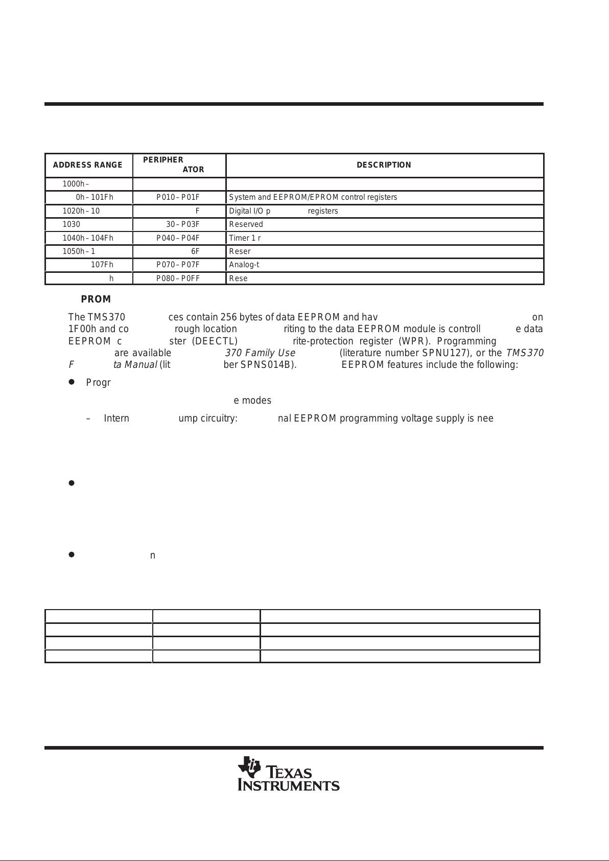
designator is P16. Table 4 shows the TMS370Cx9x peripheral files address map.
TMS370Cx9x
8-BIT MICROCONTROLLER
SPNS036B – JANUARY 1996 – REVISED FEBRUARY 1997
10
POST OFFICE BOX 1443 • HOUSTON, TEXAS 77251–1443
peripheral file (PF) (continued)
Table 4. TMS370Cx9x Peripheral File Address Map
БББББ
Á
ADDRESS RANGE
БББББ
Á
PERIPHERAL FILE
DESIGNAT OR
ББББББББББББББББББББ
Á
DESCRIPTION
1000h–100Fh
P000–P00F
Reserved
1010h–101Fh
P010–P01F
System and EEPROM/EPROM control registers
1020h–103Fh
P020–P03F
Digital I/O port control registers
1030h–103Fh
P030–P03F
Reserved
1040h–104Fh
P040–P04F
Timer 1 registers
1050h–106Fh
P050–P06F
Reserved
1070h–107Fh
P070–P07F
Analog-to-digital converter 3 registers
1080h–10FFh
P080–P0FF
Reserved
data EEPROM
The TMS370Cx9x devices contain 256 bytes of data EEPROM and have a memory map beginning at location
1F00h and continuing through location 1FFFh. Writing to the data EEPROM module is controlled by the data
EEPROM control register (DEECTL) and the write-protection register (WPR). Programming algorithm
examples are available in the
TMS370 Family User’s Guide
(literature number SPNU127), or the
TMS370
Family Data Manual
(literature number SPNS014B). The data EEPROM features include the following:
D
Programming:
– Bit, byte, and block write/erase modes
– Internal charge pump circuitry: No external EEPROM programming voltage supply is needed.
– Control register: Data EEPROM programming is controlled by the data EEPROM control register
(DEECTL) located in the PF frame beginning at location P01A.
– In-circuit programming capability: There is no need to remove the device to program.
D
Write-protection: Writes to the data EEPROM are disabled during the following conditions:
– Reset: All programming of the data EEPROM module is halted.
– Write protection active: there is one write-protect bit per 32-byte EEPROM block.
– Low-power mode operation
D
Write protection can be overridden by applying 12 V to the MC pin.
Table 5 shows the memory map of the control registers.
T able 5. Data EEPROM and Program EPROM Control Registers Memory Map
ADDRESS
SYMBOL
БББББББББББББББББББ
NAME
101Ah (P01A)
DEECTL
БББББББББББББББББББ
Data EEPROM control register
101Bh (P01B)
—
БББББББББББББББББББ
Reserved
101Ch (P01C)
EPCTL
БББББББББББББББББББ
Program EPROM control register

TMS370Cx9x
8-BIT MICROCONTROLLER
SPNS036B – JANUARY 1996 – REVISED FEBRUARY 1997
11
POST OFFICE BOX 1443 • HOUSTON, TEXAS 77251–1443
program EPROM
The TMS370C792 contains 8K bytes of program EPROM memory mapped beginning at location 6000h and
continuing through location 7FFFh as shown in Figure 3. Memory addresses 7FE0h through 7FEBh are
reserved for T exas Instruments (TI) and addresses 7FECh through 7FFFh are reserved for interrupt and reset
vectors. Trap vectors, used with TRAP0 through TRAP15 instructions, are located between addresses 7FC0h
and 7FDFh. Reading the program EPROM modules is identical to reading other internal memory. During
programming, the EPROM is controlled by the program EPROM control register (EPCTL). The program
EPROM modules’ features include:
D
Programming
– In-circuit programming capability if V
PP
is applied to the MC pin
– Control register: Program EPROM programming is controlled by the program EPROM control registers
EPCTL located at the addresses in PF frame 1 as shown in Table 5.
D
Write protection: Writes to the program EPROM are disabled under the following conditions:
– Reset: All programming to the EPROM module is halted.
– Low-power modes
– 13 V not applied to MC
program ROM
The program ROM consists of 4K bytes of mask-programmable ROM. The program ROM is used for permanent
storage of data or instructions. Programming of the mask ROM is performed at the time of device fabrication.
Memory addresses 7FE0h through 7FEBh are reserved for TI and addresses 7FECh through 7FFFh are
reserved for interrupt and reset vectors. Trap vectors, used with TRAP0 through TRAP15 instructions, are
located between addresses 7FC0h and 7FDFh.
system reset
The system-reset operation ensures an orderly start-up sequence for the TMS370Cx9x CPU-based device.
There are up to three different actions that can cause a system reset to the device. Two of these actions are
internally generated, while one (RESET) is controlled externally. These actions are as follows:
D
External RESET pin. A low level signal can trigger an external reset. To assure a reset, the external signal
should be held low for one SYSCLK cycle (it is possible, however, that a signal of less than one SYSCLK
could cause a reset). See the
TMS370 User’s Guide
(literature number SPNU127) or the
TMS370 Family
Data Manual
(SPNS014B) for more information.
D
Watchdog (WD) timer. A watchdog-generated reset occurs if an improper value is written to the WD key
register or if the re-initialization does not occur before the watchdog timer timeout . See the
TMS370 User’s
Guide
(literature number SPNU127) or the
TMS370 Family Data Manual
(SPNS014B) for more information.
D
Oscillator reset. Reset occurs when the oscillator operates outside of the recommended operating range.
See the
TMS370 User’s Guide
(literature number SPNU127) or the
TMS370 Family Data Manual
(SPNS014B) for more information.
Once a reset source is activated, the external RESET
pin is driven (active) low for a minimum of eight SYSCLK
cycles. This allows the ’x9x device to reset external system components. Additionally, if a cold start condition
(V
CC
is off for several hundred milliseconds), oscillator failure occurs, or RESET pin is held low , then the reset
logic holds the device in a reset state for as long as these actions are active.
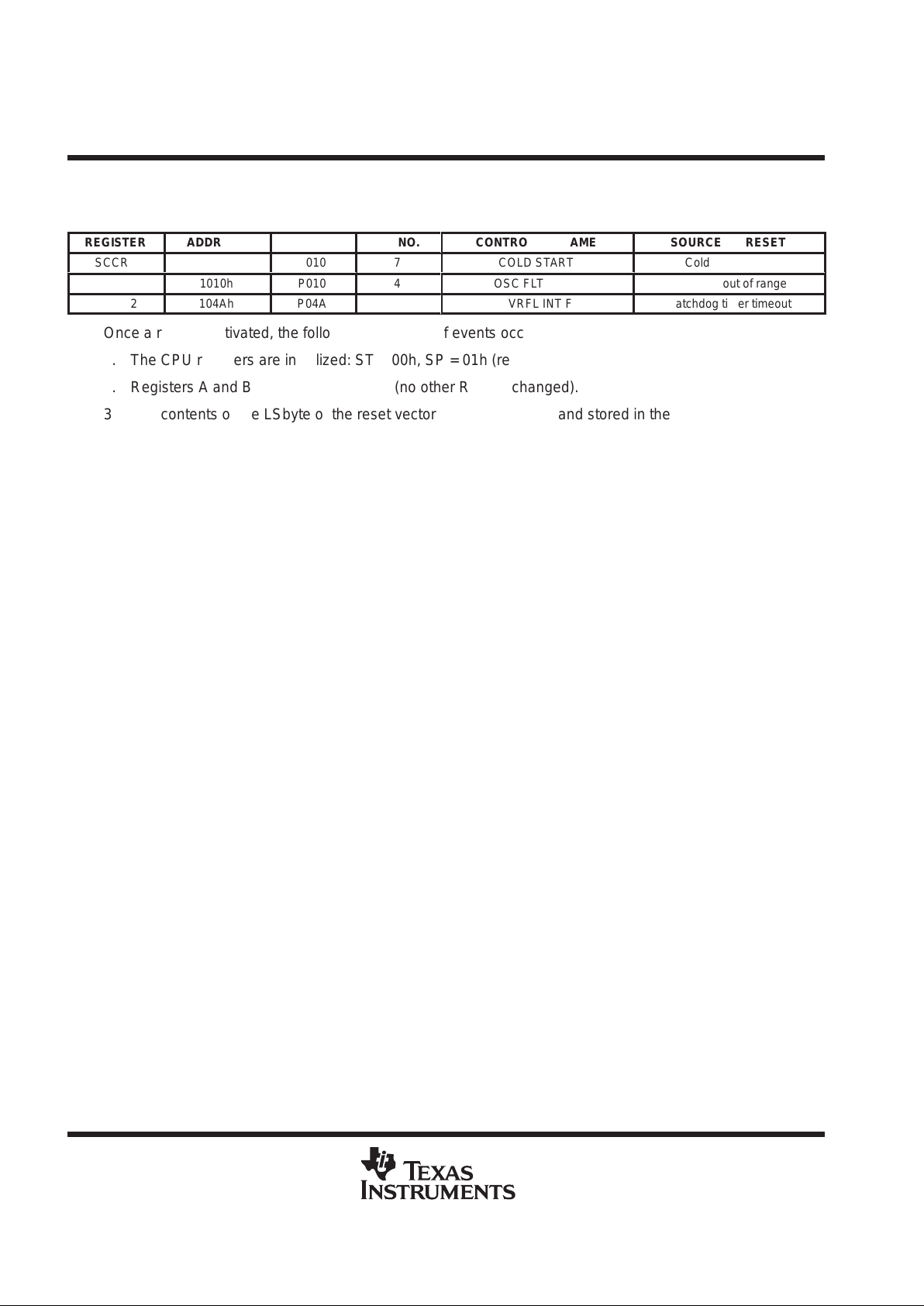
After a reset, the program can check the oscillator fault flag (OSC FLT FLAG, SCCR0.4), the cold start flag
(COLD ST ART , SCCR0.7), and the watchdog reset (WD OVRFL INT FLAG, T1CTL2.5) to determine the source
of the reset. A reset does not clear these flags. Table 6 depicts the reset sources.
TI is a trademark of Texas Instruments Incorporated.
TMS370Cx9x
8-BIT MICROCONTROLLER
SPNS036B – JANUARY 1996 – REVISED FEBRUARY 1997
12
POST OFFICE BOX 1443 • HOUSTON, TEXAS 77251–1443
system reset (continued)
Table 6. Reset Sources
REGISTER
ADDRESS
PF
BIT NO.
CONTROL BIT NAME
SOURCE OF RESET
SCCR0
1010h
P010
7
COLD START
Cold (power-up)
SCCR0
1010h
P010
4
OSC FLT FLAG
Oscillator out of range
T1CTL2
104Ah
P04A
5
WD OVRFL INT FLAG
Watchdog timer timeout
Once a reset is activated, the following sequence of events occurs:
1. The CPU registers are initialized: ST = 00h, SP = 01h (reset state).
2. Registers A and B are initialized to 00h (no other RAM is changed).
3. The contents of the LSbyte of the reset vector (07FFh) are read and stored in the PCL.
4. The contents of the MSbyte of the reset vector (07FEh) are read and stored in the PCH.
5. Program execution begins with an opcode fetch from the address pointed to by the PC.
The reset sequence takes 20 SYSCLK cycles from the time the reset pulse is released until the first opcode
fetch. During a reset, RAM contents (except for registers A and B) remain unchanged, and the module control
register bits are initialized to their reset state.
interrupts
The TMS370 family software programmable interrupt structure permits flexible on-chip and external-interrupt
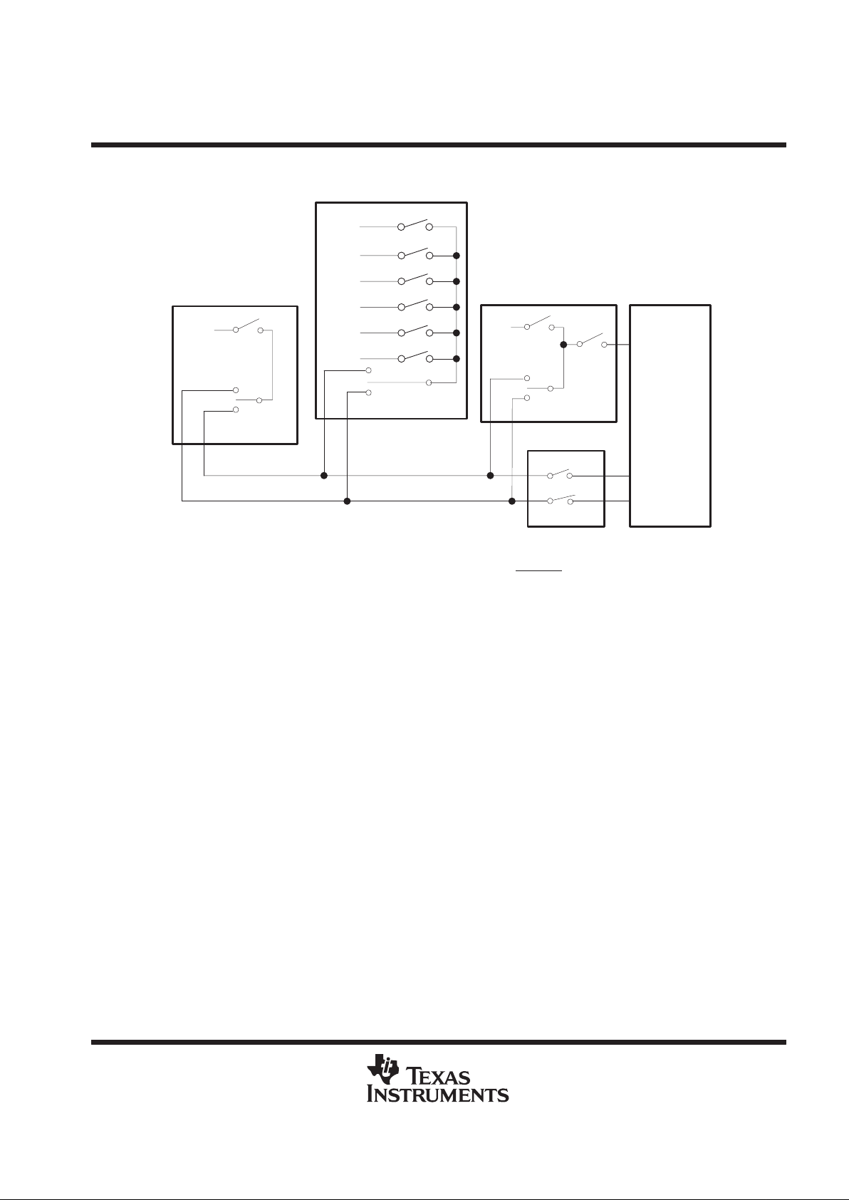
configurations to meet real-time interrupt-driven application requirements. The hardware-interrupt structure
incorporates two priority levels as shown in Figure 4. Interrupt level 1 has a higher priority than interrupt
level 2. The two priority levels can be masked independently by the global-interrupt mask bits (IE1 and IE2) of
the status register.
Each system interrupt is configured independently to either the high- or low-priority chain by the application
program during system initialization. Within each interrupt chain, the interrupt priority is fixed by the position of
the system interrupt. However, since each system interrupt is configured selectively on either the high- or
low-priority interrupt chain, the application program can elevate any system interrupt to the highest priority.
Arbitration between the two priority levels is performed within the CPU. Arbitration within each of the priority
chains is performed within the peripheral modules to support interrupt expansion for future modules. Pending
interrupts are serviced upon completion of current instruction execution, depending on their interrupt mask and
priority conditions.
TMS370Cx9x
8-BIT MICROCONTROLLER
SPNS036B – JANUARY 1996 – REVISED FEBRUARY 1997
13
POST OFFICE BOX 1443 • HOUSTON, TEXAS 77251–1443
interrupts (continued)
TIMER 1
CPU
NMI
Logic
Enable
IE1
IE2
Level 1 INT
Level 2 INT
T1 PRI
Priority
Overflow
Compare1
Ext Edge
Compare2
Input Capture 1
STATUS REG
EXT INT1
INT1 PRI
INT1
Watchdog
AD INT
AD PRI
A/D
Figure 4. Interrupt Control
The TMS370Cx9x has three hardware system interrupts (plus RESET) as shown in Table 7. Each system
interrupt has a dedicated vector located in program memory through which control is passed to the interrupt
service routines. A system interrupt can have multiple interrupt sources. All of the interrupt sources are
individually maskable by local interrupt-enable control bits in the associated PF. Each interrupt source FLAG
bit is individually readable for software polling or for determining which interrupt source generated the
associated system interrupt.
Two of the system interrupts are generated by on-chip peripheral functions, and one external interrupt is
supported. Software configuration of the external interrupt is performed through the INT1 control registers in
peripheral file frame 1. The external is software-configurable for input polarity (rising or falling edge) for ease
of system interface. External interrupt INT1 is software-configurable as either a maskable or non-maskable
interrupt. When INT1 is configured as non-maskable, it cannot be masked by the individual or global enable
mask bits. The INT1 NMI bit is protected during non-privileged operation and, therefore, should be configured
during the initialization sequence following reset. To maximize pin flexibility, external interrupt INT1 can be
software-configured as a general-purpose input pin if the interrupt function is not required.
TMS370Cx9x
8-BIT MICROCONTROLLER
SPNS036B – JANUARY 1996 – REVISED FEBRUARY 1997
14
POST OFFICE BOX 1443 • HOUSTON, TEXAS 77251–1443
interrupts (continued)
T able 7. Hardware System Interrupts
БББББББББ
Á
INTERRUPT SOURCE
БББББББ
Á
INTERRUPT FLAG
ÁÁÁÁ
Á
SYSTEM
INTERRUPT
ÁÁÁÁ
Á
VECTOR
ADDRESS
ÁÁÁÁ
Á
PRIORITY
†
БББББББББ
Á
External RESET
Watchdog overflow
Oscillator fault detect
БББББББ
Á
COLD START
WD OVRFL INT FLAG
OSC FLT FLAG
ÁÁÁÁ
Á
RESET
‡
ÁÁÁÁ
Á
7FFEh, 7FFFh
ÁÁÁÁ
Á
1
External INT1
INT1 FLAG
INT1
‡
7FFCh, 7FFDh
2
БББББББББ
Á
БББББББББ
Á
БББББББББ
Á
Timer 1 overflow
Timer 1 compare 1
Timer 1 compare 2
Timer 1 external edge
Timer 1 input capture 1
Watchdog overflow
БББББББ
Á
БББББББ
Á
БББББББ
Á
T1 OVRFL INT FLAG
T1C1 INT FLAG
T1C2 INT FLAG
T1EDGE INT FLAG
T1IC1 INT FLAG
WD OVRFL INT FLAG
ÁÁÁÁ
Á
ÁÁÁÁ
Á
ÁÁÁÁ
Á
T1INT
§
ÁÁÁÁ
Á
ÁÁÁÁ
Á
ÁÁÁÁ
Á
7FF4h, 7FF5h
ÁÁÁÁ
Á
ÁÁÁÁ
Á
ÁÁÁÁ
Á
3
A/D conversion complete
AD INT FLAG
ADINT
7FECh, 7FEDh
4
†
Relative priority within an interrupt level.
‡
Releases microcontroller from STANDBY and HALT low-power modes.
§
Releases microcontroller from STANDBY low-power mode.
privileged operation and EEPROM write-protection override
The TMS370Cx9x family has significant flexibility to enable the designer to software-configure the system and
peripherals to meet the requirements of a broad variety of applications. The nonprivileged mode of operation
ensures the integrity of the system configuration, once it is defined for an application. Following a hardware
reset, the TMS370Cx9x operates in the privileged mode, where all peripheral file registers have unrestricted
read/write access, and the application program configures the system during the initialization sequence
following reset. As the last step of system initialization, the PRIVILEGE DISABLE bit (SCCR2.0) should be set
to one to enter the nonprivileged mode; disabling write operations to specific configuration control bits within
the peripheral file. Table 8 displays the system configuration bits that are write-protected during the
nonprivileged mode and must be configured by software prior to exiting the privileged mode.
Table 8. Privilege Bits
REGISTER
¶
NAME
LOCATION
CONTROL BIT
ÁÁÁÁ
Á
SCCRO
ÁÁÁ
Á
P010.6
P010.6
БББББББББ
Á
PF AUTO WAIT
OSC POWER
SCCR1
P011.2
P011.4
MEMORY DISABLE
AUTOWAIT DISABLE
ÁÁÁÁ
Á
ÁÁÁÁ
Á
ÁÁÁÁ
Á
SCCR2
ÁÁÁ
Á
ÁÁÁ
Á
ÁÁÁ
Á
P012.0
P012.1
P012.3
P012.4
P012.6
P012.7
БББББББББ
Á
БББББББББ
Á
БББББББББ
Á
PRIVILEGE DISABLE
INT1 NMI
CPU STEST
BUS STEST
PWRDWN/IDLE
HALT/STANDBY
ÁÁÁÁ
Á
T1PRI
ÁÁÁ
Á
P04F.6
P04F.7
БББББББББ
Á
T1 PRIORITY
T1 STEST
ÁÁÁÁ
Á
ADPRI
ÁÁÁ
Á
P07F.5
P07F.6
P07F.7
БББББББББ
Á
AD ESPEN
AD PRIORITY
AD STEST
¶
The privilege bits are shown in a bold typeface in the system configuration
registers section.
TMS370Cx9x
8-BIT MICROCONTROLLER
SPNS036B – JANUARY 1996 – REVISED FEBRUARY 1997
15
POST OFFICE BOX 1443 • HOUSTON, TEXAS 77251–1443
privileged operation and EEPROM write-protection override (continued)
The write-protect override (WPO) mode provides an external hardware method of overriding the
write-protection registers of data EEPROM on the TMS370Cx9x. Applying a 12-V input to the MC pin after the
RESET input goes high (logic 1) enters the WPO mode. The high voltage on MC during the WPO mode is not
the programming voltage for the data EEPROM or program EPROM. All EEPROM programming voltages are
generated on-chip. The WPO mode provides hardware system level capability to modify the content of the data
EEPROM while the device remains in the application, but only while requiring a 12-V external input on the MC
pin (normally not available in the end application except in a service or diagnostic environment).
low-power and IDLE modes
The TMS370Cx9x devices have two low-power modes (STANDBY and HALT) and an IDLE mode. For
mask-ROM devices, low-power modes can be disabled permanently through a programmable contact at the
time when the mask is manufactured.
The STANDBY and HALT low power modes significantly reduce power consumption by reducing or stopping
the activity of the various on-chip peripherals when processing is not required. Each of the low-power modes
is entered by executing the idle instruction when the PWRDWN/IDLE bit in register SCCR2 has been set to one.
The HALT/STANDBY bit in SCCR2 controls which low-power mode is entered.
In the ST ANDBY mode (HAL T/STANDBY = 0), all CPU activity and most peripheral module activity is stopped;
however, the oscillator, internal clocks, and timer 1 remain active. System processing is suspended until a
qualified interrupt (hardware RESET
, external interrupt on INT1, or timer 1 interrupt) is detected.
In the HAL T mode (HALT/STANDBY = 1), the TMS370Cx9x is placed in its lowest power-consumption mode.
The oscillator and internal clocks are stopped, causing all internal activity to be halted. System activity is
suspended until a qualified interrupt (hardware RESET or an external interrupt on INT1) is detected. The
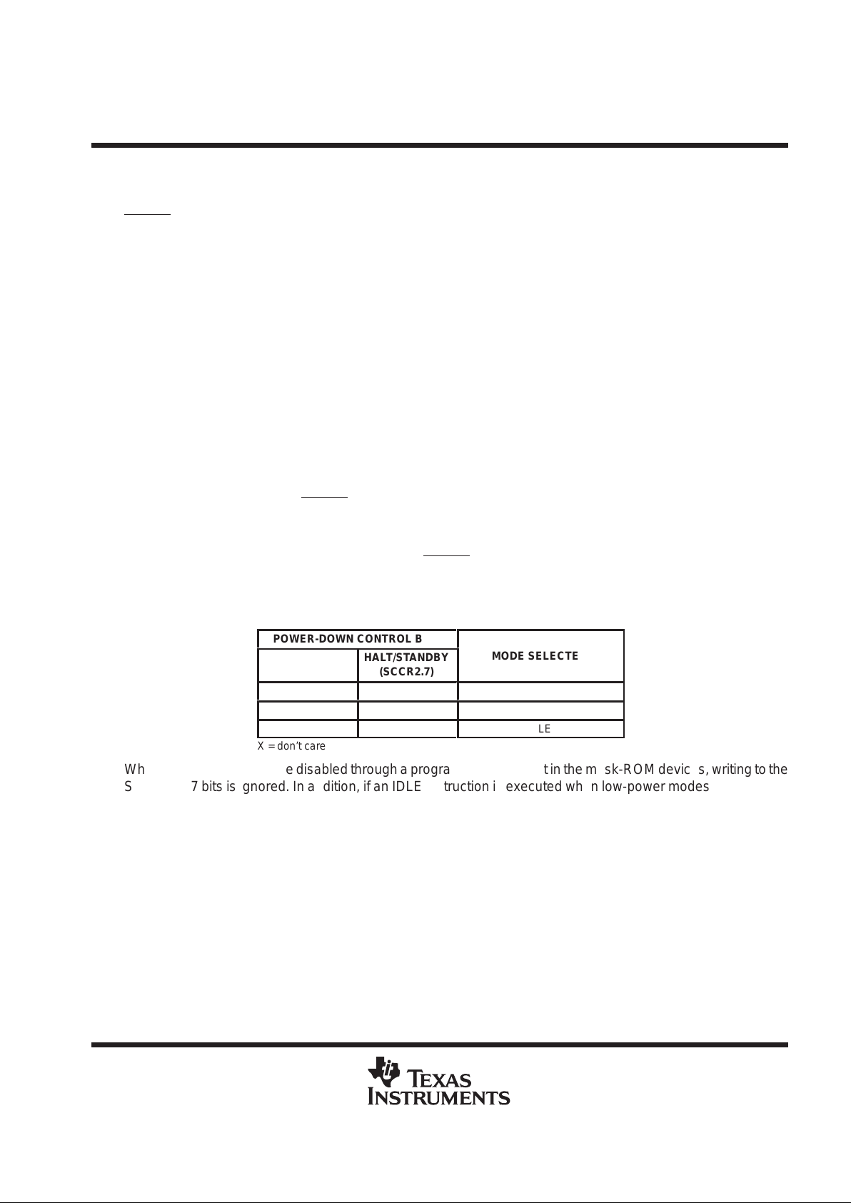
low-power mode selection bits are summarized in Table 9.
Table 9. Low-Power/Idle Control Bits
POWER-DOWN CONTROL BITS
ÁÁÁ
Á
PWRDWN/IDLE
(SCCR2.6)
ÁÁÁÁ
Á
HALT/STANDBY
(SCCR2.7)
БББББББ
Á
MODE SELECTED
1
0
STANDBY
1
1
HALT
0
X
IDLE
X = don’t care
When low-power modes are disabled through a programmable contact in the mask-ROM devices, writing to the
SCCR2.6–7 bits is ignored. In addition, if an IDLE instruction is executed when low-power modes are disabled
through a programmable contact, the device always enters the IDLE mode.
T o provide a method of always exiting low-power modes for mask-ROM devices, INT1 is enabled automatically
as a nonmaskable interrupt (NMI) during low-power modes when the hard watchdog mode is selected. This
means that the NMI is always generated, regardless of the interrupt enable flags.
The following information is preserved throughout both the STANDBY and HALT modes: RAM (register file),
CPU registers (stack pointer, program counter , and status register), I/O pin direction and output data, and status
registers of all on-chip peripheral functions. Since all CPU instruction processing is stopped during the
STANDBY and HALT modes, the clocking of the watchdog timer is inhibited.

TMS370Cx9x
8-BIT MICROCONTROLLER
SPNS036B – JANUARY 1996 – REVISED FEBRUARY 1997
16
POST OFFICE BOX 1443 • HOUSTON, TEXAS 77251–1443
clock modules
The ‘370Cx9x family provides two clock options which are referred to as divide-by-1 (PLL) and divide-by-4
(standard oscillator). Both the divide-by-1 and divide-by-4 options are configurable during the manufacturing
process of a TMS370 microcontroller. The ‘370C090A ROM-masked devices of fer both options to meet system
engineering requirements. Only one of the two clock options is allowed on the ROM device while the EPROM
device ’792 has only the divide-by-4 clock.
The divide-by-1 clock module option provides the capability for reduced electromagnetic interference (EMI) with
no added cost.
The divide-by-1 provides a 1-to-1 match of the external resonator frequency (CLKIN) to the internal system clock
(SYSCLK) frequency. The divide-by-4 produces a SYSCLK which is one-fourth the frequency of the external
resonator. Inside the divide-by-1 module, the frequency of the external resonator is multiplied by four . The clock
module then divides the resulting signal by four to provide the four-phased internal system clock signals. The
resulting SYSCLK is equal to the resonator frequency. The frequencies are formulated as follows:
Divide-by-4 option : SYSCLK
+
external resonator frequency
4
+
CLKIN
4
Divide-by-1 option : SYSCLK
+
external resonator frequency 4
4
+
CLKIN
The main advantage of choosing a divide-by-1 oscillator is that EMI is reduced. The harmonics of low-speed
resonators extend through less of the emissions spectrum than the harmonics of faster resonators. The
divide-by-1 provides the capability of reducing the resonator speed by four times, and this results in a steeper
decay of emissions produced by the oscillator.
TMS370Cx9x
8-BIT MICROCONTROLLER
SPNS036B – JANUARY 1996 – REVISED FEBRUARY 1997
17
POST OFFICE BOX 1443 • HOUSTON, TEXAS 77251–1443
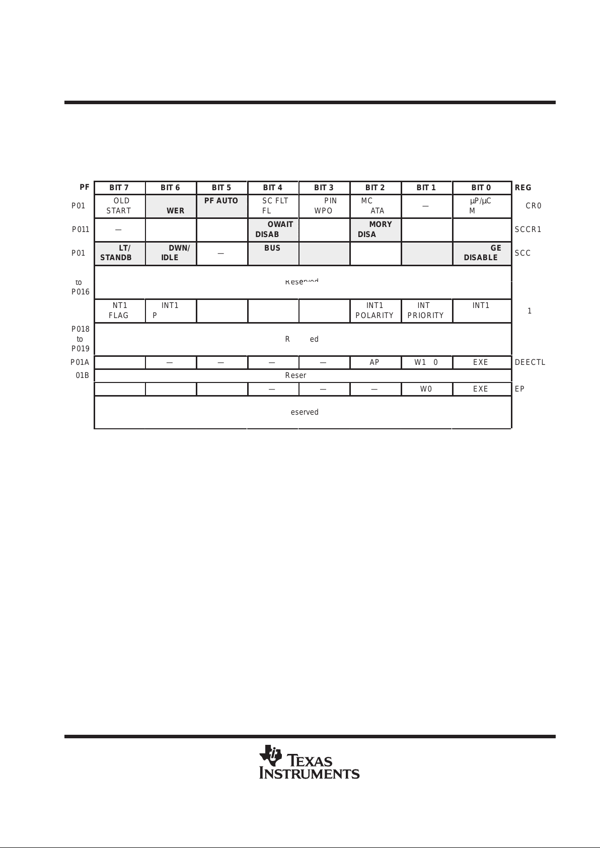
system configuration registers
Table 10 contains system configuration and control functions and registers for controlling EEPROM
programming. The privileged bits are shown in a bold typeface and shaded.
Table 10. Peripheral File Frame 1: System Configuration Registers
PF
BIT 7
BIT 6
BIT 5
BIT 4
BIT 3
BIT 2
BIT 1
BIT 0
REG
Á
Á
P010
ÁÁ
Á
COLD
START
OSC
POWER
PF AUTO
WAIT
ÁÁ
Á
OSC FLT
FLAG
ÁÁÁ
Á
MC PIN
WPO
ÁÁ
Á
MC PIN
DATA
ÁÁÁ
Á
—
ÁÁ
Á
µP/µC
MODE
ÁÁ
Á
SCCR0
P011
—
—
—
AUTOWAIT
DISABLE
—
MEMORY
DISABLE
—
—
SCCR1
Á
Á
P012
HALT/
STANDBY
PWRDWN/
IDLE
ÁÁ
Á
—
BUS
STEST
CPU
STEST
ÁÁ
Á
—
INT1
NMI
PRIVILEGE
DISABLE
ÁÁ
Á
SCCR2
P013
t
o
P016
Reserved
Á
Á
P017
ÁÁ
Á
INT1
FLAG
ÁÁÁ
Á
INT1
PIN DATA
ÁÁ
Á
—
ÁÁ
Á
—
ÁÁÁ
Á
—
ÁÁ
Á
INT1
POLARITY
ÁÁÁ
Á
INT1
PRIORITY
ÁÁ
Á
INT1
ENABLE
ÁÁ
Á
INT1
Á
Á
P018
to
P019
ББББББББББББББББББББББББББ
Á
Reserved
ÁÁ
Á
P01A
BUSY
—
—
—
—
AP
W1W0
EXE
DEECTL
P01B Reserved
P01C
BUSY
VPPS
—
—
—
—
W0
EXE
EPCTL
Á
Á
Á
Á
P01D
to
P01F
Reserved
ÁÁ
Á
ÁÁ
Á
 Loading...