

Page 1
V
(MAX)
T
A
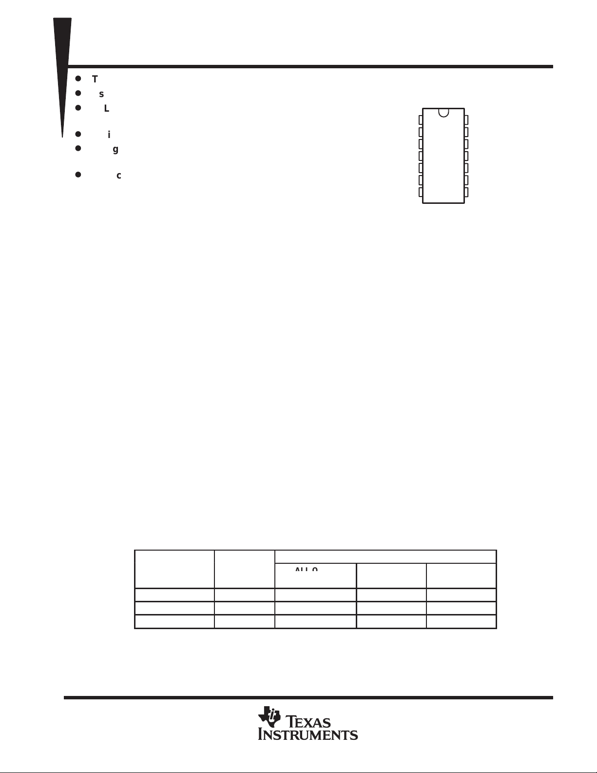
SMALL OUTLINE
CERAMIC DIP
PLASTIC DIP
(D)
(J)
(N)
现货库存、技术资料、百科信息、热点资讯,精彩尽在鼎好!
NE556, SA556, SE556
DUAL PRECISION TIMERS
SLFS023C – APRIL 1978 – REVISED DECEMBER 1999
D
Two Precision Timing Circuits per Package
D
Astable or Monostable Operation
D
TTL-Compatible Output Can Sink or Source
Up to 150 mA
D
Active Pullup or Pulldown
D
Designed to be Interchangeable With
Signetics NE556, SA556, and SE556
D
Applications Include:
– Precision Timers From Microseconds to
Hours
– Pulse-Shaping CIrcuits
– Missing-Pulse Detectors
– Tone-Burst Generators
– Pulse-Width Modulators
– Pulse-Position Modulators
– Sequential Timers
– Pulse Generators
– Frequency Dividers
– Application Timers
– Industrial Controls
– Touch-Tone Encoders
description
NE556, SA556 . . . D, OR N PACKAGE
SE556 ...J PACKAGE
(TOP VIEW)
1DISCH
1THRES
1CONT
1RESET
1OUT
1TRIG
GND
1
2
3
4
5
6
7
14
13
12
11
10
9
8
V
CC
2DISCH
2THRES
2CONT
2RESET
2OUT
2TRIG
These devices provide two independent timing circuits of the NE555, SA555, or SE555 type in each package.
These circuits can be operated in the astable or the monostable mode with external resistor-capacitor (RC)
timing control. The basic timing provided by the RC time constant can be controlled actively by modulating the
bias of the control-voltage input.
The threshold (THRES) and trigger (TRIG) levels are normally two-thirds and one-third, respectively , of V
CC
These levels can be altered by using the control-voltage (CONT) terminal. When the trigger input falls below
trigger level, the flip-flop is set and the output goes high. If the trigger input is above the trigger level and the
threshold input is above the threshold level, the flip-flop is reset and the output is low. The reset (RESET) input
can override all other inputs and can be used to initiate a new timing cycle. When the reset input goes low, the
flip-flop is reset and the output goes low. When the output is low, a low-impedance path is provided between
the discharge (DISCH) terminal and ground (GND).
The NE556 is characterized for operation from 0°C to 70°C. The SA556 is characterized for operation from
–40°C to 85°C, and the SE556 is characterized for operation over the full military range of –55°C to 125°C.
AVAILABLE OPTIONS
T
VCC = 15 V
0°C to 70°C 11.2 V NE556D – NE556N
–40°C to 85°C 11.2 V SA556D – SA556N
–55°C to 125°C 10.6 V – SE556J –
The D package is available taped and reeled. Add the suffix R to the device type (e.g., NE556DR).
PACKAGED DEVICES
.
PRODUCTION DATA information is current as of publication date.
Products conform to specifications per the terms of Texas Instruments
standard warranty. Production processing does not necessarily include
testing of all parameters.
POST OFFICE BOX 655303 • DALLAS, TEXAS 75265
Copyright 1999, Texas Instruments Incorporated
On products compliant to MIL-PRF-38535, all parameters are tested
unless otherwise noted. On all other products, production
processing does not necessarily include testing of all parameters.
1
Page 2
NE556, SA556, SE556
DUAL PRECISION TIMERS
SLFS023C – APRIL 1978 – REVISED DECEMBER 1999
RESET
Low Irrelevant Irrelevant Low On
High < 1/3 V
High > 1/3 V
High > 1/3 V
†
Voltage levels shown are nominal.
functional block diagram, each timer
TRIGGER VOLTAGE†THRESHOLD VOLTAGE†OUTPUT DISCHARGE SWITCH
DD
DD
DD
FUNCTION TABLE
(each timer)
Irrelevant High Off
> 2/3 V
> 2/3 V
DD
DD
Low On
As previously established
CC
R
THRES
CONT
R
TRIG
R
GND
RESET can override TRIG, which can override THRES.
RESETV
R1
RS1
OUT
DISCH
absolute maximum ratings over operating free-air temperature range (unless otherwise noted)
Supply voltage, VCC (see Note 1) 18 V. . . . . . . . . . . . . . . . . . . . . . . . . . . . . . . . . . . . . . . . . . . . . . . . . . . . . . . . . . . .
Input voltage (CONT, RESET, THRES, and TRIG) V
Output current ±225 mA. . . . . . . . . . . . . . . . . . . . . . . . . . . . . . . . . . . . . . . . . . . . . . . . . . . . . . . . . . . . . . . . . . . . . . . . .
Continuous total dissipation See Dissipation Rating Table. . . . . . . . . . . . . . . . . . . . . . . . . . . . . . . . . . . . . . . . . . .
Package thermal impedance, θJA (see Note 2): D package 86°C/W. . . . . . . . . . . . . . . . . . . . . . . . . . . . . . . . . .
Lead temperature 1,6 mm (1/16 inch) from case for 60 seconds: J package 300°C. . . . . . . . . . . . . . . . . . . . .
Lead temperature 1,6 mm (1/16 inch) from case for 10 seconds: D or N package 260°C. . . . . . . . . . . . . . . .
Storage temperature range, T
‡
Stresses beyond those listed under “absolute maximum ratings” may cause permanent damage to the device. These are stress ratings only, and
functional operation of the device at these or any other conditions beyond those indicated under “recommended operating conditions” is not
implied. Exposure to absolute-maximum-rated conditions for extended periods may affect device reliability.
NOTES: 1. All voltage values are with respect to network ground terminal.
2. The package thermal impedance is calculated in accordance with JESD 51.
–65°C to 150°C. . . . . . . . . . . . . . . . . . . . . . . . . . . . . . . . . . . . . . . . . . . . . . . . . . .
stg
. . . . . . . . . . . . . . . . . . . . . . . . . . . . . . . . . . . . . . . . . . . . . .
N package 80°C/W. . . . . . . . . . . . . . . . . . . . . . . . . . . . . . . . . .
‡
CC
DISSIPATION RATING TABLE
PACKAGE
J 1375 mW 11.0 mW/°C 880 mW 715 mW 275 mW
2
TA ≤ 25°C
POWER RATING
DERATING FACTOR
ABOVE TA = 25°C
POST OFFICE BOX 655303 • DALLAS, TEXAS 75265
TA = 70°C
POWER RATING
TA = 85°C
POWER RATING
TA = 125°C
POWER RATING
Page 3
Suppl
oltage, V
V
PARAMETER
TEST CONDITIONS
UNIT
VTThreshold voltage level
V
V
Trigger voltage level
V
I
Reset current
mA
V
Control voltage (open circuit)
V
V
V
VOLLow-level output voltage
V
V
V
V
15 V
,
mA
ICCSupply current
g
nA
recommended operating conditions
pp
y v
Input voltage (CONT, RESET, THRES, and TRIG), V
Output current, I
Operating free-air temperature, T
CC
O
A
NE556, SA556, SE556
DUAL PRECISION TIMERS
SLFS023C – APRIL 1978 – REVISED DECEMBER 1999
MIN MAX UNIT
NE556, SA556 4.5 16
SE556 4.5 18
I
NE556 0 70
SA556 –40 85
SE556 –55 125
V
CC
±200 mA
V
°C
electrical characteristics, V
I
T
TRIG
I
TRIG
V
RESET
RESET
I
DISCH
CONT
V
OH
NOTE 3: This parameter influences the maximum value of the timing resistors RA and RB in the circuit of Figure 1. For example, when
Threshold current (see Note 3) 30 250 30 250 nA
Trigger current TRIG at 0 V 0.5 2 0.5 0.9 µA
Reset voltage level 0.3 0.7 1 0.3 0.7 1 V
Discharge switch off-state
current
p
p
High-level output voltage
pp
VCC = 5 V, the maximum value is R = RA + RB ≈ 3.4 MΩ, and for VCC = 15 V, the maximum value is ≈ 10 MΩ.
= 5 V to 15 V, TA = 25°C (unless otherwise noted)
CC
NE556, SA556 SE556
MIN TYP MAX MIN TYP MAX
VCC = 15 V 8.8 10 11.2 9.4 10 10.6
VCC = 5 V 2.4 3.3 4.2 2.7 3.3 4
VCC = 15 V 4.5 5 5.6 4.8 5 5.2
VCC = 5 V 1.1 1.67 2.2 1.45 1.67 1.9
RESET at V
RESET at 0 V –0.4 1.5 –0.4 –1
VCC = 15 V 9 10 11 9.6 10 10.4
VCC = 5 V 2.6 3.3 4 2.9 3.3 3.8
CC
CC
CC
VCC = 5 V IOH = –100 mA 2.75 3.3 3 3.3
Output low,
No Load
Output high,
No load
= 15
= 5
=
CC
IOL = 10 mA 0.1 0.25 0.1 0.15
IOL = 50 mA 0.4 0.75 0.4 0.5
IOL = 100 mA 2 2.5 2 2.2
IOL = 200 mA 2.5 2.5
IOL = 5 mA 0.1 0.25 0.1 0.15
IOL = 8 mA 0.15 0.3 0.15 0.25
IOH = –100 mA 12.75 13.3 13 13.3
IOH = –200 mA 12.5 12.5
VCC = 15 V 20 30 20 24
VCC = 5 V 6 12 6 10
VCC = 15 V 18 26 18 20
VCC = 5 V 4 10 4 8
0.1 0.4 0.1 0.4
20 100 20 100 nA
V
POST OFFICE BOX 655303 • DALLAS, TEXAS 75265
3
Page 4

NE556, SA556, SE556
PARAMETER
UNIT
‡
g
timing interval
timing interval
L
ns
DUAL PRECISION TIMERS
SLFS023C – APRIL 1978 – REVISED DECEMBER 1999
operating characteristics, VCC = 5 V and 15 V
TEST
CONDITIONS
Each timer, monostable
Initial error of timing interval
Temperature coefficient of
Supply voltage sensitivity of
Output pulse rise time
Output pulse fall time
†
For conditions shown as MIN or MAX, use the appropriate value specified under recommended operating conditions.
‡
Timing interval error is defined as the difference between the measured value and the average value of a random sample from each process
run.
§
Values specified are for a device in a monostable circuit similar to Figure 2, with component values as follow: RA = 2 kΩ to 100 kΩ, C = 0.1µF.
¶
Values specified are for a device in an astable circuit similar to Figure 1, with component values as follow: RA = 1 kΩ to 100 kΩ, C = 0.1µF.
Each timer, astable
Timer 1 — Timer 2 ±1 ±0.5
Each timer, monostable
Each timer, astable
Timer 1 — Timer 2 ±10 ±10
Each timer, monostable
Each timer, astable
Timer 1 — Timer 2 ±0.2 ±0.1
§
¶
§
¶
§
¶
TA = 25°C
TA = MIN to MAX
TA = 25°C
CL = 15 pF,
TA = 25°C
†
NE556, SA556 SE556
MIN TYP MAX MIN TYP MAX
1 3 0.5 1.5
2.25% 1.5%
50 30 100
150 90
0.1 0.5 0.05 0.2
0.3 0.15
100 300 100 200
100 300 100 200
ppm/°C
%/V
APPLICATION INFORMATION
V
CC
(5 V to 15 V)
Open
(see Note A)
R
A
R
B
NOTE A: Bypassing the control-voltage input to ground with
a capacitor may improve operation. This should be
evaluated for individual applications.
CONT
RESET
DISCH
THRES
TRIG
C
Figure 1. Circuit for Astable Operation
V
CC
OUT
GND
R
L
OUT
V
CC
(5 V to 15 V)
0.01 µF
V
CC
OUT
GND
INPUT
R
A
C
CONT
RESET
DISCH
THRES
TRIG
Figure 2. Circuit for Monostable Operation
R
L
OUT
4
POST OFFICE BOX 655303 • DALLAS, TEXAS 75265
Page 5

IMPORTANT NOTICE
T exas Instruments and its subsidiaries (TI) reserve the right to make changes to their products or to discontinue
any product or service without notice, and advise customers to obtain the latest version of relevant information
to verify, before placing orders, that information being relied on is current and complete. All products are sold
subject to the terms and conditions of sale supplied at the time of order acknowledgement, including those
pertaining to warranty, patent infringement, and limitation of liability.
TI warrants performance of its semiconductor products to the specifications applicable at the time of sale in
accordance with TI’s standard warranty. Testing and other quality control techniques are utilized to the extent
TI deems necessary to support this warranty . Specific testing of all parameters of each device is not necessarily
performed, except those mandated by government requirements.
CERTAIN APPLICATIONS USING SEMICONDUCTOR PRODUCTS MAY INVOLVE POTENTIAL RISKS OF
DEATH, PERSONAL INJURY, OR SEVERE PROPERTY OR ENVIRONMENTAL DAMAGE (“CRITICAL
APPLICATIONS”). TI SEMICONDUCTOR PRODUCTS ARE NOT DESIGNED, AUTHORIZED, OR
WARRANTED TO BE SUITABLE FOR USE IN LIFE-SUPPORT DEVICES OR SYSTEMS OR OTHER
CRITICAL APPLICA TIONS. INCLUSION OF TI PRODUCTS IN SUCH APPLICATIONS IS UNDERST OOD TO
BE FULLY AT THE CUSTOMER’S RISK.
In order to minimize risks associated with the customer’s applications, adequate design and operating
safeguards must be provided by the customer to minimize inherent or procedural hazards.
TI assumes no liability for applications assistance or customer product design. TI does not warrant or represent
that any license, either express or implied, is granted under any patent right, copyright, mask work right, or other
intellectual property right of TI covering or relating to any combination, machine, or process in which such
semiconductor products or services might be or are used. TI’s publication of information regarding any third
party’s products or services does not constitute TI’s approval, warranty or endorsement thereof.
Copyright 1999, Texas Instruments Incorporated
 Loading...