

Product
Folder
Sample &
Buy
Technical
Documents
Tools &
Software
Support &
Community
RF430FRL15xH NFC ISO 15693 Sensor Transponder
1 Device Overview
1.1 Features
1
• ISO/IEC 15693, ISO/IEC 18000-3 (Mode 1)
Compliant RF Interface
• Power Supply System With Either Battery or
13.56-MHz H-Field Supply
• 14-Bit Sigma-Delta Analog-to-Digital Converter
(ADC)
• Internal Temperature Sensor
• Resistive Sensor Bias Interface
• CRC16 CCITT Generator
• MSP430™ Mixed-Signal Microcontroller
– 2KB of FRAM
– 4KB of SRAM
– 8KB of ROM
– Supply Voltage Range: 1.45 V to 1.65 V
– Low Power Consumption
• Active Mode (AM): 140 µA/MHz (1.5 V)
• Standby Mode (LPM3): 16 µA
– 16-Bit RISC Architecture
– Up to 2-MHz CPU System Clock
– Compact Clock System
• 4-MHz High-Frequency Clock
RF430FRL152H, RF430FRL153H, RF430FRL154H
SLAS834C –NOVEMBER 2012–REVISED DECEMBER 2014
• 256-kHz Internal Low-Frequency Clock
Source
• External Clock Input
– 16-Bit Timer_A With Three Capture/Compare
Registers
– LV Port Logic
• VOLLower Than 0.15 V at 400 µA
• VOHHigher Than (V
– 0.15 V) at 400 µA
DDB
• Timer_A PWM Signal Available on All Ports
– eUSCI_B Module Supports 3-Wire and 4-Wire
SPI and I2C
– 32-Bit Watchdog Timer (WDT_A)
– ROM Development Mode (Map ROM Addresses
to SRAM to Enable Firmware Development)
– Full 4-Wire JTAG Debug Interface
• For Complete Module Descriptions, See the
RF430FRL15xH Family Technical Reference
Manual (SLAU506)
• For Application Operation and Programming, See
the RF430FRL15xH Firmware User's Guide
(SLAU603)
1.2 Applications
• Industrial Wireless Sensors • Medical Wireless Sensors
1.3 Description
The RF430FRL15xH device is a 13.56-MHz transponder chip with a programmable 16-bit MSP430™ lowpower microcontroller. The device features embedded universal FRAM nonvolatile memory for storage of
program code or user data such as calibration and measurement data. The RF430FRL15xH supports
communication, parameter setting, and configuration through the ISO/IEC 15693, ISO/IEC 18000-3
compliant RFID interface and the SPI or I2C interface. Sensor measurements are supported by the
internal temperature sensor and the onboard 14-bit sigma-delta analog-to-digital converter (ADC), and
digital sensors can be connected through SPI or I2C.
The RF430FRL15xH device is optimized for operation in fully passive (battery-less) or single-cell batterypowered (semi-active) mode to achieve extended battery life in portable and wireless sensing applications.
FRAM is a nonvolatile memory that combines the speed, flexibility, and endurance of SRAM with the
stability and reliability of flash, all at lower total power consumption.
1
An IMPORTANT NOTICE at the end of this data sheet addresses availability, warranty, changes, use in safety-critical applications,
intellectual property matters and other important disclaimers. PRODUCTION DATA.
eUSCI_B0
SPI
I C
2
8KB
ROM
CPU and
Working
Registers
4W-JTAG
Reset
Int-Logic
VDDB
TMS, TCK,
TDI, TDO
P1.0 to P1.7
RST/NMI
Debug
support
ANT
1
ANT
2
VSS
VDDH
CLKIN
VDDSW
VDD2X
CP1
CP2
VDDD
4KB
RAM
2KB
FRAM
CRC
16 bit
Timer_A
3 CC
Registers
IO Port
8 I/Os
with
interrupt
capability
14-Bit
Sigma-
Delta
ADC
ISO
15693
Decode
and
Encode
Watchdog
WDTA
32/16 Bit
ISO
15693
Analog
Front End
Power
Supply
System
MAB
LF-OSC
HF-OSC
ACLK
SMCLK
MCLK
Clock
System
C
RES
L
RES
ADC0/ADC1/ADC2
TEMP1/TEMP2
RF430FRL152H, RF430FRL153H, RF430FRL154H
SLAS834C –NOVEMBER 2012–REVISED DECEMBER 2014
www.ti.com
PART NUMBER PACKAGE BODY SIZE
RF430FRL152H VQFN (24) 4 mm x 4 mm
RF430FRL153H VQFN (24) 4 mm x 4 mm
RF430FRL154H VQFN (24) 4 mm x 4 mm
(1) For the most current part, package, and ordering information for all available devices, see the Package
Option Addendum in Section 9, or see the TI web site at www.ti.com.
(2) The sizes shown here are approximations. For the package dimensions with tolerances, see the
Mechanical Data in Section 9.
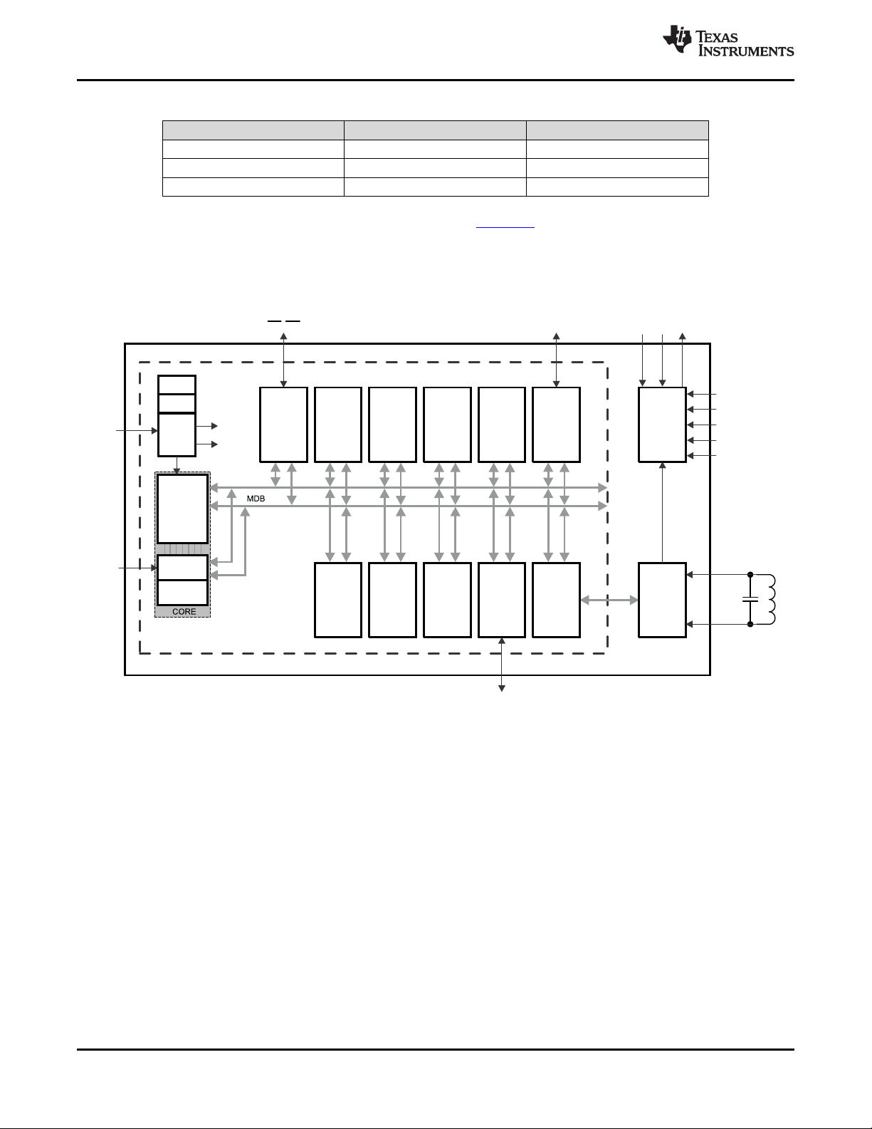
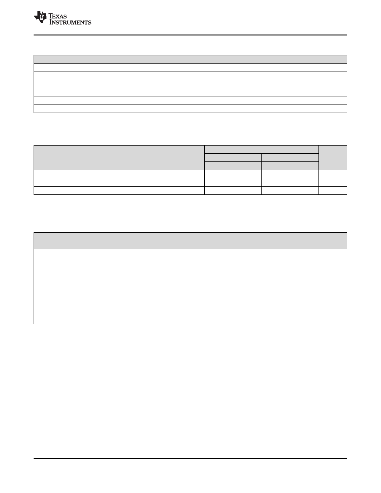
1.4 Functional Block Diagram
Figure 1-1 shows the block diagram of the RF430FRL15xH device.
Device Information
(1)
(2)
2 Device Overview Copyright © 2012–2014, Texas Instruments Incorporated
Figure 1-1. Functional Block Diagram
Submit Documentation Feedback
Product Folder Links: RF430FRL152H RF430FRL153H RF430FRL154H
RF430FRL152H, RF430FRL153H, RF430FRL154H
www.ti.com
SLAS834C –NOVEMBER 2012–REVISED DECEMBER 2014
Table of Contents
1 Device Overview ......................................... 1 5.18 RFPMM, Power Supply Switch ..................... 19
1.1 Features .............................................. 1 5.19 RFPMM, Bandgap Reference....................... 19
1.2 Applications........................................... 1 5.20 RFPMM, Voltage Doubler........................... 19
1.3 Description............................................ 1 5.21 RFPMM, Voltage Supervision ...................... 19
1.4 Functional Block Diagram ............................ 2 5.22 SD14, Performance ................................. 20
2 Revision History ......................................... 4 5.23 SVSS Generator .................................... 20
3 Device Comparison ..................................... 5 5.24 Thermistor Bias Generator.......................... 21
4 Terminal Configuration and Functions.............. 6 5.25 Temperature Sensor ................................ 21
4.1 Pin Diagram .......................................... 6
4.2 Signal Descriptions ................................... 7
4.3 Pin Multiplexing....................................... 9
4.4 Connections for Unused Pins ........................ 9
5 Specifications........................................... 10
5.1 Absolute Maximum Ratings ........................ 10
5.2 ESD Ratings ........................................ 10
5.3 Recommended Operating Conditions............... 10
5.4 Recommended Operating Conditions, Resonant
Circuit................................................ 11 6.5 Memory.............................................. 26
5.5 Active Mode Supply Current Into V
External Current .................................... 11
5.6 Low-Power Mode Supply Current (Into V
Excluding External Current.......................... 11
5.7 Digital I/Os (P1, RST/NMI).......................... 12
5.8 High-Frequency Oscillator (4 MHz), HFOSC ....... 12
5.9 Low-Frequency Oscillator (256 kHz), LFOSC ...... 12
5.10 Wake-Up From Low-Power Modes ................. 13
5.11 Timer_A ............................................. 13
5.12 eUSCI (SPI Master Mode) Recommended
Operating Conditions................................ 14
5.13 eUSCI (SPI Master Mode) .......................... 14
5.14 eUSCI (SPI Slave Mode) ........................... 16
5.15 eUSCI (I
5.16 FRAM................................................ 18
5.17 JTAG ................................................ 18
2
C Mode)................................... 18
DDB
Excluding
)
DDB
5.26 RF13M, Power Supply and Recommended
Operating Conditions................................ 21
5.27 RF13M, ISO/IEC 15693 ASK Demodulator......... 21
5.28 RF13M, ISO/IEC 15693 Compliant Load Modulator 21
6 Detailed Description ................................... 22
6.1 CPU ................................................. 22
6.2 Instruction Set....................................... 22
6.3 Operating Modes.................................... 23
6.4 Interrupt Vector Addresses.......................... 24
6.6 Peripherals .......................................... 27
6.7 Port Schematics..................................... 33
6.8 Device Descriptors (TLV) ........................... 41
7 Applications, Implementation, and Layout ....... 42
8 Device and Documentation Support ............... 43
8.1 Device Support...................................... 43
8.2 Documentation Support ............................. 44
8.3 Related Links........................................ 44
8.4 Community Resources .............................. 45
8.5 Trademarks.......................................... 45
8.6 Electrostatic Discharge Caution..................... 45
8.7 Glossary............................................. 45
9 Mechanical Packaging and Orderable
Information .............................................. 45
9.1 Packaging Information .............................. 45
Copyright © 2012–2014, Texas Instruments Incorporated Table of Contents 3
Submit Documentation Feedback
Product Folder Links: RF430FRL152H RF430FRL153H RF430FRL154H

RF430FRL152H, RF430FRL153H, RF430FRL154H
SLAS834C –NOVEMBER 2012–REVISED DECEMBER 2014
www.ti.com
2 Revision History
NOTE: Page numbers for previous revisions may differ from page numbers in the current version.
Changes from November 13, 2014 to December 8, 2014 Page
• Corrected all instances of the title of the RF430FRL15xH Family Technical Reference Manual .......................... 1
• Corrected all instances of the title of the RF430FRL15xH Firmware User's Guide ......................................... 1
• Moved T
• Changed title of Section 5.2 to ESD Ratings.................................................................................... 10
to Absolute Maximum Ratings table ................................................................................ 10
stg
4 Revision History Copyright © 2012–2014, Texas Instruments Incorporated
Submit Documentation Feedback
Product Folder Links: RF430FRL152H RF430FRL153H RF430FRL154H
www.ti.com
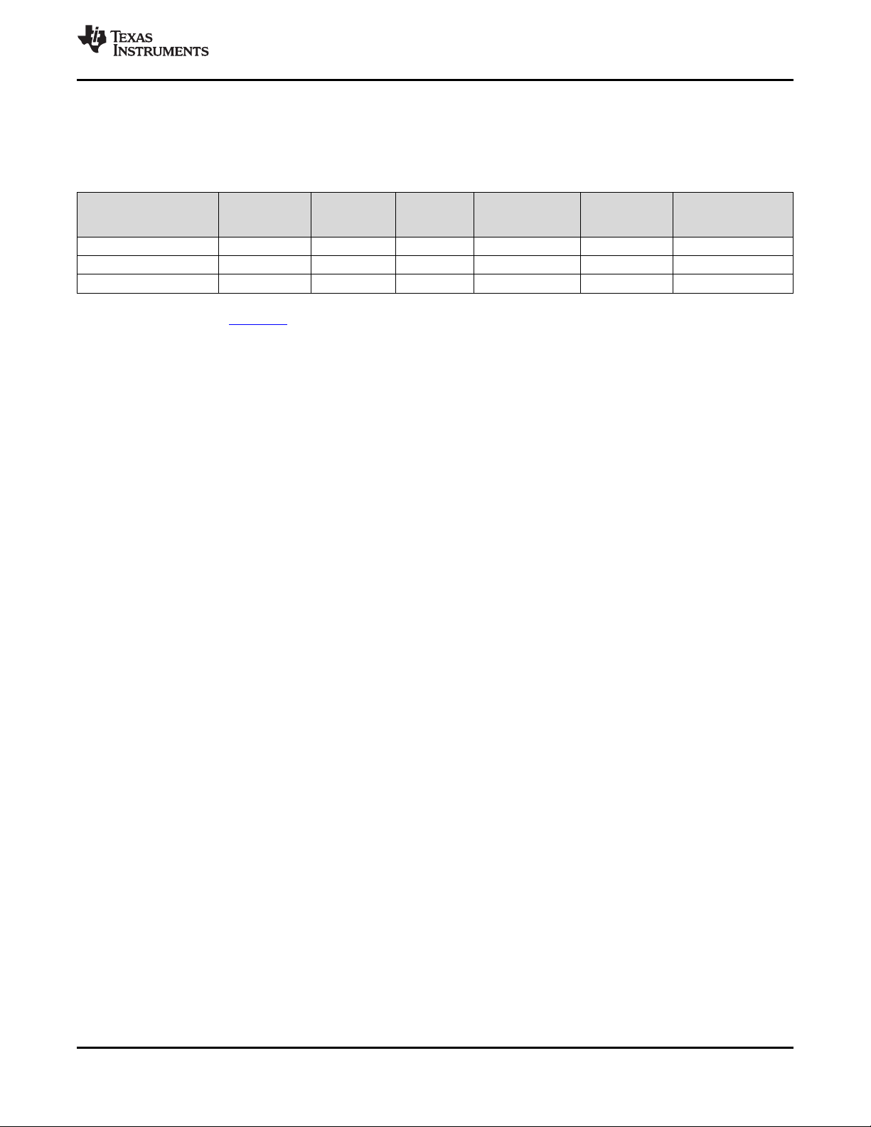
3 Device Comparison
Table 3-1 summarizes the available family members.
RF430FRL152H, RF430FRL153H, RF430FRL154H
SLAS834C –NOVEMBER 2012–REVISED DECEMBER 2014
Table 3-1. Device Comparison
Device Timer ISO/IEC 15693 eUSCI_B SD14
RF430FRL152H 2 4 Yes Yes Yes Yes
RF430FRL153H 2 4 Yes Yes No Yes
RF430FRL154H 2 4 Yes Yes Yes No
(1) For the most current part, package, and ordering information for all available devices, see the Package Option Addendum in Section 9,
or see the TI web site at www.ti.com.
FRAM SRAM
(KB) (KB)
(1)
13.56-MHz
Front End
Copyright © 2012–2014, Texas Instruments Incorporated Device Comparison 5
Submit Documentation Feedback
Product Folder Links: RF430FRL152H RF430FRL153H RF430FRL154H
VSS
Exposed die
attached pad
ADC2/TEMP2
SVSS
ADC1/TEMP1
TST1
TST2
ADC0
VDD2X
P1.3/SPI_STE/TA0.2/ACLK/TA0CLK
P1.2/SPI_CLK/MCLK/TA0.0
RST/NMI
P1.1/SPI_SOMI/SCL/ACLK/TA0.2/CCI0.0
VDDD
VDDH
TCK/P1.4/TA0.1/SMCLK/CCI0.1
TDI/P1.5/TA0.2/MCLK/CCI0.1
TDO/P1.6/TA0.0/TA0.2/CCI0.2
TMS/P1.7/TA0.1/TA0.0/CCI0.2
ANT1
VDDB
ANT2
VDDSW
CP1
CP2
1
2
3
4
5
6
18
17
16
15
14
13
7 8 9 10 11 12
24 23 22 21 20 19
RF430FRL152H, RF430FRL153H, RF430FRL154H
SLAS834C –NOVEMBER 2012–REVISED DECEMBER 2014
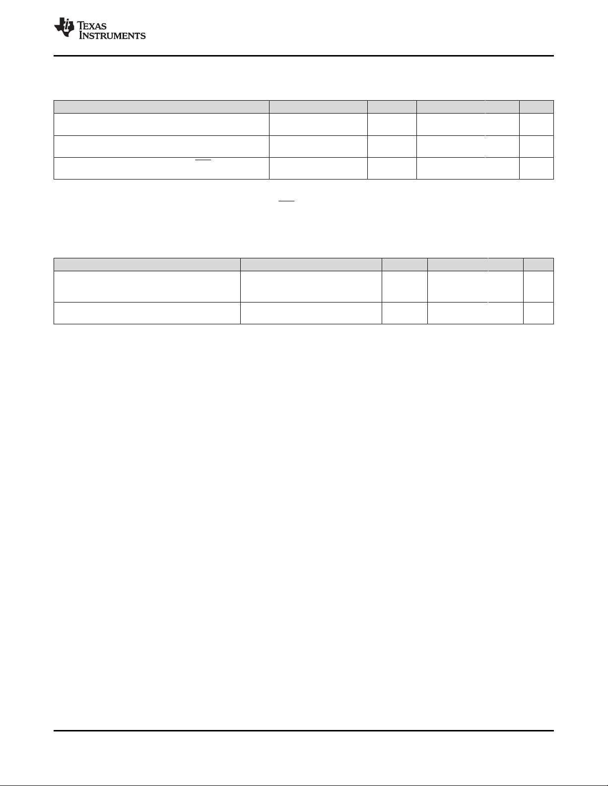
4 Terminal Configuration and Functions
4.1 Pin Diagram
Figure 4-1 shows the pin assignments on the 24-pin RGE package.
www.ti.com
Figure 4-1. 24-Pin RGE Package (Top View)
Product Folder Links: RF430FRL152H RF430FRL153H RF430FRL154H
Submit Documentation Feedback
6 Terminal Configuration and Functions Copyright © 2012–2014, Texas Instruments Incorporated
RF430FRL152H, RF430FRL153H, RF430FRL154H
www.ti.com
SLAS834C –NOVEMBER 2012–REVISED DECEMBER 2014
4.2 Signal Descriptions
Table 4-1 describes the signals.
Table 4-1. Signal Descriptions
TERMINAL
NAME NO.
ANT1 1 I Antenna input 1
ANT2 2 I Antenna input 2
V
V
DDSW
DDB
3 Switched supply voltage
4 Battery supply voltage
CP1 5 Charge pump flying cap terminal 1
CP2 6 Charge pump flying cap terminal 2
V
DD2X
7 Voltage doubler output
P1.3 General-purpose digital I/O
SPI_STE SPI slave transmit enable
TA0.2 Timer_A TA0 OUT2 output
8 I/O
ACLK ACLK output (divided by 1, 2, 4, 8, 16, or 32)
TA0CLK Timer_A TA0 clock signal TA0CLK input
I/O
(1)
DESCRIPTION
P1.2 General-purpose digital I/O
SPI_CLK SPI clock
9 I/O
MCLK MCLK output
TA0.0 Timer_A TA0 OUT0 output
RST/NMI 10 I
Reset input active low
Non-maskable interrupt input
P1.1 General-purpose digital I/O
SPI_SOMI SPI slave out master in
SCL I2C clock
11 I/O
ACLK ACLK output (divided by 1, 2, 4, or 8 )
TA0.2 Timer_A TA0 OUT2 output
CCI0.0 Timer_A TA0 CCR0 capture: CCI0B input, compare
P1.0 General-purpose digital I/O
SPI_SIMO SPI slave in master out
SDA I2C data
12 I/O
SMCLK SMCLK output
TA0.1 Timer0_A3 OUT1 output
CCI0.0 Timer_A TA0 CCR0 capture: CCI0A input, compare
ADC0 13 I ADC input pin 0
TST2 14 Internal; connect to GND
SVSS 15 Sensor reference potential
TST1 16 Internal; connect to GND
ADC1 / TEMP1 17 ADC input pin 1 / Resistive bias pin 1
ADC2 / TEMP2 18 ADC input pin 2 / Resistive bias pin 2
(1) I = input, O = output
Copyright © 2012–2014, Texas Instruments Incorporated Terminal Configuration and Functions 7
Submit Documentation Feedback
Product Folder Links: RF430FRL152H RF430FRL153H RF430FRL154H
RF430FRL152H, RF430FRL153H, RF430FRL154H
SLAS834C –NOVEMBER 2012–REVISED DECEMBER 2014
Table 4-1. Signal Descriptions (continued)
TERMINAL
NAME NO.
TMS JTAG test mode select
P1.7 General-purpose digital I/O
TA0.1 Timer_A TA0 OUT1 output
19 I/O
TA0.0 Timer_A TA0 OUT0 output
CCI0.2 Timer_A TA0 CCR2 capture: CCI2B input, compare
TDO JTAG test data output
P1.6 General-purpose digital I/O
TA0.0 Timer_A TA0 OUT0 output
20 I/O
TA0.2 Timer_A TA0 OUT2 output
CCI0.2 Timer_A TA0 CCR2 capture: CCI2A input, compare
TDI JTAG test data input
P1.5 General-purpose digital I/O
TA0.2 Timer_A TA0 OUT2 output
21 I/O
MCLK MCLK output
CCI0.1 Timer_A TA0 CCR1 capture: CCI1B input, compare
I/O
(1)
DESCRIPTION
www.ti.com
TCK JTAG test clock
P1.4 General-purpose digital I/O
TA0.1 Timer_A TA0 OUT1 output
22 I/O
SMCLK SMCLK output
CCI0.1 Timer_A TA0 CCR1 capture: CCI1A input, compare
CLKIN External clock input pin
V
DDH
V
DDD
V
SS
23 O Rectified voltage from RF-AFE
24 Digital supply voltage
Pad Ground reference, bonded to exposed pad
(2)
(2) VSS combines both digital ground (DVSS) and analog ground (AVSS)
8 Terminal Configuration and Functions Copyright © 2012–2014, Texas Instruments Incorporated
Submit Documentation Feedback
Product Folder Links: RF430FRL152H RF430FRL153H RF430FRL154H
RF430FRL152H, RF430FRL153H, RF430FRL154H
www.ti.com
SLAS834C –NOVEMBER 2012–REVISED DECEMBER 2014
4.3 Pin Multiplexing
The GPIO port pins are multiplexed with other functions including analog peripherals and serial
communication modules. The pin functions are selected by a combination of register values and device
modes. For schematics of the port pins and details of the multiplexing for each, refer to Section 6.7.
4.4 Connections for Unused Pins
The correct termination of all unused pins is listed in Table 4-2.
Table 4-2. Connection of Unused Pins
Pin Potential Comment
TDI/TMS/TCK Open When used for JTAG function
RST/NMI VCCor V
Px.0 to Px.7 Open Set to port function, output direction
TDO Open Convention: leave TDO terminal as JTAG function
SS
10-nF capacitor to GND/V
SS
Copyright © 2012–2014, Texas Instruments Incorporated Terminal Configuration and Functions 9
Submit Documentation Feedback
Product Folder Links: RF430FRL152H RF430FRL153H RF430FRL154H
RF430FRL152H, RF430FRL153H, RF430FRL154H
SLAS834C –NOVEMBER 2012–REVISED DECEMBER 2014
5 Specifications
www.ti.com
5.1 Absolute Maximum Ratings
(1)
over recommended ranges of supply voltage and operating free-air temperature (unless otherwise noted)
MIN MAX UNIT
Voltage applied at V
Voltage applied at V
Voltage applied to any pin (references to VSS) -0.3 V
Diode current at any device pin
Current derating factor when I/O ports are switched in parallel electrically and logically
Storage temperature range, T
referenced to VSS(V
DDB
referenced to VSS(V
ANT
(2)
(4) (5) (6)
stg
) -0.3 1.65 V
AMR
) -0.3 3.6 V
AMR
+ 0.3 V
DDB
±2 mA
(3)
0.9
-40 125 °C
(1) Stresses beyond those listed under Absolute Maximum Ratings may cause permanent damage to the device. These are stress ratings
only, and functional operation of the device at these or any other conditions beyond those indicated under Recommended Operating
Conditions is not implied. Exposure to absolute-maximum-rated conditions for extended periods may affect device reliability.
(2) All voltages are referenced to VSS.
(3) The diode current increases to ±4.5 mA when two pins are connected, it increases to ±6.75 mA when three pins are connected, and so
on.
(4) Soldering during board manufacturing must follow the current JEDEC J-STD-020 specification with peak reflow temperatures not higher
than classified on the device label on the shipping boxes or reels. If hand soldering is required for application prototyping, peak
temperature must not exceed 250°C for a total of 5 minutes for any single device.
(5) Data retention on FRAM memory cannot be ensured when exceeding the specified maximum storage temperature, T
(6) Programming of devices with user application code should only be performed after reflow or hand soldering. Factory programmed
.
stg
information, such as calibration values, are designed to withstand the temperatures reached in the current JEDEC J-STD-020
specification.
5.2 ESD Ratings
VALUE UNIT
V
ESD
Electrostatic discharge (ESD)
performance
Human body model (HBM), per ANSI/ESDA/JEDEC JS001
(1) JEDEC document JEP155 states that 500-V HBM allows safe manufacturing with a standard ESD control process.
(2) Low leakage pin: ADC0 has reduced ESD tolerance of ±500 V HBM.
(1)(2)
±2000 V
5.3 Recommended Operating Conditions
Typical data are based on V
V
DDB
V
SS
T
A
C
VDDB
C
VDDSW
C
FLY
C
VDD2X
C
VDDD
C
SVSS
f
SYSTEM
f
CLKIN
(1) Low equivalent series resistance (ESR) capacitor
(2) The MSP430 CPU is clocked directly with MCLK. Both the high and low phase of MCLK must not exceed the pulse duration of the
specified maximum frequency.
(3) Modules may have a different maximum input clock specification. See the specification of the respective module in this data sheet.
Supply voltage during program execution 1.45 1.65 V
Supply voltage (GND reference) 0 V
Operating free-air temperature 0 70 °C
Capacitor on V
Capacitor on V
Charge pump capacitor between CP1 and CP2.
Recommended ratio between C
Capacitor on V
Recommended ratio between C
Capacitor on V
Capacitor between SVSS and V
System frequency
External clock input frequency 32 kHz
= 1.5 V, TA= 25°C (unless otherwise noted)
DDB
(1)
DDB
(1)
DDSW
DD2x
DDD
.
(1)
(2) (3)
FLY
FLY
SS
and C
and C
(1)
VDD2X
VDD2X
is ≥ 1:10.
is ≥ 1:10.
MIN NOM MAX UNIT
100 nF
2.2 µF
(1)
(1)
10 nF
100 nF
1 µF
1 µF
2 MHz
10 Specifications Copyright © 2012–2014, Texas Instruments Incorporated
Submit Documentation Feedback
Product Folder Links: RF430FRL152H RF430FRL153H RF430FRL154H
RF430FRL152H, RF430FRL153H, RF430FRL154H
www.ti.com
SLAS834C –NOVEMBER 2012–REVISED DECEMBER 2014
5.4 Recommended Operating Conditions, Resonant Circuit
MIN NOM MAX UNIT
f
c
V
ANT_peak
Z Impedance of LC circuit 6.5 15.5 kΩ
L
RES
C
RES
QT Tank quality factor 30
(1) See the RF13M parameter section.
Carrier frequency 13.56 MHz
Antenna input voltage 3.6 V
Coil inductance 2.66 µH
Resonance capacitance 51.8 – C
(1)
IN
pF
5.5 Active Mode Supply Current Into V
over recommended operating free-air temperature (unless otherwise noted)
PARAMETER V
EXECUTION
MEMORY
Excluding External Current
DDB
(1)
Frequency (f
DDB
1 MHz 2 MHz UNIT
MCLK
= f
SMCLK
TYP MAX TYP MAX
I
AM, FRAM
I
AM, RAM
I
AM, ROM
(2)
(2)
(2)
FRAM 1.5 V 330 420 480 580 µA
RAM 1.5 V 220 300 250 320 µA
ROM 1.5 V 220 300 230 300 µA
(1) All inputs are tied to 0 V or to VCC. Outputs do not source or sink any current.
(2) f
5.6 Low-Power Mode Supply Current (Into V
= 256 kHz, CPUOFF = 0, SCG0 = 0, SCG1 = 0, OSCOFF = 0
ACLK
) Excluding External Current
DDB
over recommended ranges of supply voltage and operating free-air temperature (unless otherwise noted)
0ºC 20ºC 45ºC 70ºC
TYP MAX TYP MAX TYP MAX TYP MAX
I
LPM0
PARAMETER V
f
= off, f
MCLK
(2)
1 MHz, f
ACLK
CPUOFF = 1, SCG0 = 0,
SMCLK
= 32 kHz,
=
DDB
1.5 V 170 230 190 210 260 340 µA
SCG1 = 0, OSCOFF = 0
f
I
LPM3
= f
MCLK
f
(3)
= 16 kHz,
ACLK
CPUOFF = 1, SCG0 = 1,
SMCLK
= off,
1.5 V 12 20 13 16 25 65 µA
SCG1 = 1, OSCOFF = 0
f
I
LPM4
= f
MCLK
(4)
0 Hz
CPUOFF = 1, SCG0 = 1,
SMCLK
= f
ACLK
=
1.5 V 11 16 12 15 24 60 µA
SCG1 = 1, OSCOFF = 1
(1) Including current for WDT clocked by ACLK.
(2) CSS: SELM=SELS=HF_CLK, SELA=LF_CLK, DIVM=/2 (2MHz), DIVS=/4 (1MHz), DIVA=/8 (32kHz)
SD14: reset values
RFPMM: battery switch on (EN_BATSWITCH=1)
(3) CSS: SELM=HF_CLK, SELS=SELA=LF_CLK, DIVM=/2 (2MHz), DIVS=/32 (8kHz), DIVA=/16 (16kHz)
SD14: reset values
RFPMM: EN_BATSWITCH=1(battery switch enabled)
(4) CSS: SELM=HF_CLK, SELS=SELA=LF_CLK, DIVM=/2 (2MHz), DIVS=/32 (8kHz), DIVA=/16 (16kHz)
SD14: reset values
RFPMM: EN_BATSWITCH=1(battery switch enabled)
)
(1)
UNIT
Copyright © 2012–2014, Texas Instruments Incorporated Specifications 11
Submit Documentation Feedback
Product Folder Links: RF430FRL152H RF430FRL153H RF430FRL154H
RF430FRL152H, RF430FRL153H, RF430FRL154H
SLAS834C –NOVEMBER 2012–REVISED DECEMBER 2014
www.ti.com
5.7 Digital I/Os (P1, RST/NMI)
over recommended ranges of supply voltage and operating free-air temperature (unless otherwise noted)
PARAMETER TEST CONDITIONS MIN TYP MAX UNIT
V
V
V
V
I
I
I
t
R
R
R
C
OH
OL
IH
IL
OH
OL
LKG
INT
PULL
RST
EXT
EXT
High-level output voltage V
Low-level output voltage V
High-level input voltage V
Low-level input voltage V
High-level output current V
Low-level output current V
High-impedance leakage current V
External interrupt timing
(3)
Pullup or pulldown resistor 30 35 40 kΩ
= 1.5 V, IOH= -400 µA
DDB
= 1.5 V, IOL= 400 µA
DDB
= 1.5 V V
DDB
= 1.5 V V
DDB
= 1.45 V to 1.65 V for port P1 -400 µA
DDB
= 1.45 V to 1.65 V for port P1 400 µA
DDB
= 1.45 V to 1.65 V -100 100 nA
DDB
P1.x, V
V
DDB
For pulldown: VIN= V
= 1.45 V to 1.65 V 200 ns
DDB
=1.5 V, For pullup: VIN= VSS,
Pullup on RST/NMI 30 35 40 kΩ
External pullup resistor on RST
terminal (optional)
External capacitor on RST terminal 10 nF
(1)
for port P1 V
(2)
for port P1 0.15 V
for port P1
DDB
(1) The maximum total current IOH, for all outputs combined should not exceed 500 µA to hold the maximum voltage drop specified, limited
by low leakage switches.
(2) The maximum total current IOL, for all outputs combined should not exceed 500 µA to hold the maximum voltage drop specified.
(3) An external signal sets the interrupt flag every time the minimum interrupt pulse duration t
INT
is met.
V
DDB
– 0.15
0.7 ×
V
DDB
0.3 ×
V
DDB
47 kΩ
5.8 High-Frequency Oscillator (4 MHz), HFOSC
over recommended ranges of supply voltage and operating free-air temperature (unless otherwise noted)
PARAMETER TEST CONDITIONS MIN TYP MAX UNIT
f
HFOSC
Duty cycle 45% 50% 55%
t
START
±20% 3.04 3.8 4.56 MHz
1 µs
5.9 Low-Frequency Oscillator (256 kHz), LFOSC
over recommended ranges of supply voltage and operating free-air temperature (unless otherwise noted)
PARAMETER TEST CONDITIONS MIN TYP MAX UNIT
f
LFO
Duty cycle 45% 50% 55%
t
START
trimmed ±5% 243 256 269 kHz
11 µs
12 Specifications Copyright © 2012–2014, Texas Instruments Incorporated
Submit Documentation Feedback
Product Folder Links: RF430FRL152H RF430FRL153H RF430FRL154H
RF430FRL152H, RF430FRL153H, RF430FRL154H
www.ti.com
SLAS834C –NOVEMBER 2012–REVISED DECEMBER 2014
5.10 Wake-Up From Low-Power Modes
over recommended ranges of supply voltage and operating free-air temperature (unless otherwise noted)
t
WAKE-UP LPM0
t
WAKE-UP LPM34
t
WAKE-UP RESET
PARAMETER TEST CONDITIONS V
Wake-up time from LPM0 to active
(1)
mode
Wake-up time from LPM3 or LPM4 to
active mode
Wake-up time from RST to active
mode.
(1)
V
(2)
stable 1.5 V 210 310 µs
DDB
DDB
1.5 V 3.2 6 µs
1.5 V 160 260 µs
(1) The wake-up time is measured from the edge of an external wake-up signal (for example, port interrupt or wake-up event) until the first
instruction of the user program is fetched. This time includes the activation of the FRAM during wake-up. f
(2) The wake-up time is measured from the rising edge of the RST signal until the first instruction of the user program is fetched. This time
includes the activation of the FRAM during wake-up. f
MCLK
= 2 MHz.
MIN TYP MAX UNIT
= 2 MHz.
MCLK
5.11 Timer_A
over recommended ranges of supply voltage and operating free-air temperature (unless otherwise noted)
f
TA
t
TA,cap
PARAMETER TEST CONDITIONS V
DDB
Internal: SMCLK, ACLK
Timer_A input clock frequency External: TACLK 1.5 V 4 MHz
Duty cycle = 50% ± 10%
Timer_A capture timing 1.5 V 20 ns
All capture inputs, Minimum pulse
duration required for capture
MIN TYP MAX UNIT
Copyright © 2012–2014, Texas Instruments Incorporated Specifications 13
Submit Documentation Feedback
Product Folder Links: RF430FRL152H RF430FRL153H RF430FRL154H
RF430FRL152H, RF430FRL153H, RF430FRL154H
SLAS834C –NOVEMBER 2012–REVISED DECEMBER 2014
www.ti.com
5.12 eUSCI (SPI Master Mode) Recommended Operating Conditions
f
eUSCI
PARAMETER CONDITIONS V
eUSCI input clock frequency 1.5 V f
Internal: SMCLK, ACLK
Duty cycle = 50% ± 10%
DDB
MIN TYP MAX UNIT
SYSTEM
MHz
5.13 eUSCI (SPI Master Mode)
over recommended ranges of supply voltage and operating free-air temperature (unless otherwise noted)
PARAMETER TEST CONDITIONS V
UCSTEM = 0,
t
STE,LEAD
STE lead time, STE active to clock
UCMODEx = 01 or 10
UCSTEM = 1,
UCMODEx = 01 or 10
UCSTEM = 0,
t
STE,LAG
STE lag time, Last clock to STE UCxCLK
inactive cycles
UCMODEx = 01 or 10
UCSTEM = 1,
UCMODEx = 01 or 10
UCSTEM = 0,
t
STE,ACC
STE access time, STE active to SIMO
data out
UCMODEx = 01 or 10
UCSTEM = 1,
UCMODEx = 01 or 10
UCSTEM = 0,
t
STE,DIS
STE disable time, STE inactive to
SIMO high impedance
UCMODEx = 01 or 10
UCSTEM = 1,
UCMODEx = 01 or 10
t
SU,MI
t
HD,MI
t
VALID,MO
t
HD,MO
(1) f
For the slave's parameters t
(2) Specifies the time to drive the next valid data to the SIMO output after the output changing UCLK clock edge. See the timing diagrams
SOMI input data setup time 1.5 V 35 ns
SOMI input data hold time 1.5 V 0 ns
SIMO output data valid time
SIMO output data hold time
UCxCLK
= 1/2t
LO/HI
with t
LO/HI
= max(t
SU,SI(Slave)
(2)
(3)
VALID,MO(eUSCI)
and t
UCLK edge to SIMO valid,
CL= 20 pF
CL= 20 pF 1.5 V 0 ns
+ t
VALID,SO(Slave)
SU,SI(Slave)
, t
SU,MI(eUSCI)
see the SPI parameters of the attached slave.
+ t
VALID,SO(Slave)
DDB
1.5 V 1
1.5 V 1
1.5 V 1
1.5 V 1
1.5 V 55
1.5 V 35
1.5 V 40
1.5 V 30
1.5 V 30 ns
).
in Figure 5-1 and Figure 5-2.
(3) Specifies how long data on the SIMO output is valid after the output changing UCLK clock edge. Negative values indicate that the data
on the SIMO output can become invalid before the output changing clock edge observed on UCLK. See the timing diagrams in Figure 5-
1 and Figure 5-2.
MIN TYP MAX UNIT
(1)
UCxCLK
cycles
ns
ns
14 Specifications Copyright © 2012–2014, Texas Instruments Incorporated
Submit Documentation Feedback
Product Folder Links: RF430FRL152H RF430FRL153H RF430FRL154H
t
SU,MI
t
HD,MI
UCLK
SOMI
SIMO
t
VALID,MO
CKPL = 0
CKPL = 1
t
LOW/HIGHtLOW/HIGH
1/f
UCxCLK
t
STE,LEAD
t
STE,LAG
t
STE,ACC
t
STE,DIS
UCMODEx = 01
UCMODEx = 10
STE
t
SU,MI
t
HD,MI
UCLK
SOMI
SIMO
t
VALID,MO
CKPL = 0
CKPL = 1
t
LOW/HIGHtLOW/HIGH
1/f
UCxCLK
STE
t
STE,LEAD
t
STE,LAG
t
STE,ACC
t
STE,DIS
UCMODEx = 01
UCMODEx = 10
www.ti.com
RF430FRL152H, RF430FRL153H, RF430FRL154H
SLAS834C –NOVEMBER 2012–REVISED DECEMBER 2014
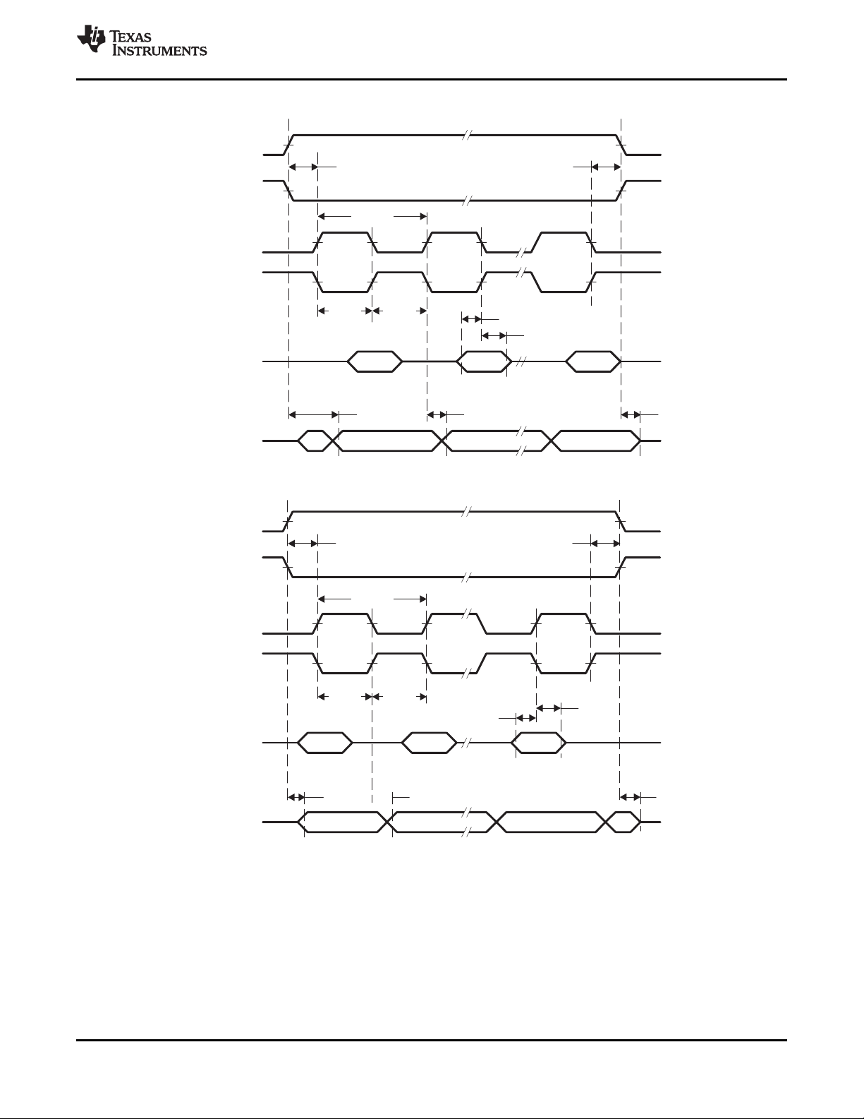
Figure 5-1. SPI Master Mode, CKPH = 0
Figure 5-2. SPI Master Mode, CKPH = 1
Copyright © 2012–2014, Texas Instruments Incorporated Specifications 15
Product Folder Links: RF430FRL152H RF430FRL153H RF430FRL154H
Submit Documentation Feedback
RF430FRL152H, RF430FRL153H, RF430FRL154H
SLAS834C –NOVEMBER 2012–REVISED DECEMBER 2014
www.ti.com
5.14 eUSCI (SPI Slave Mode)
over recommended ranges of supply voltage and operating free-air temperature (unless otherwise noted)
PARAMETER TEST CONDITIONS V
t
STE,LEAD
t
STE,LAG
t
STE,ACC
t
STE,DIS
t
SU,SI
t
HD,SI
t
VALID,SO
t
HD,SO
(1) f
For the master's parameters t
(2) Specifies the time to drive the next valid data to the SOMI output after the output changing UCLK clock edge. See the timing diagrams
STE lead time, STE active to clock 1.5 V 7 ns
STE lag time, Last clock to STE inactive 1.5 V 0 ns
STE access time, STE active to SOMI data out 1.5 V 65 ns
STE disable time, STE inactive to SOMI high
impedance
SIMO input data setup time 1.5 V 2 ns
SIMO input data hold time 1.5 V 5 ns
SOMI output data valid time
SOMI output data hold time
UCxCLK
= 1/2t
LO/HI
with t
LO/HI
(2)
(3)
≥ max(t
VALID,MO(Master)
SU,MI(Master)
and t
VALID,MO(Master)
UCLK edge to SOMI valid,
CL= 20 pF
CL= 20 pF 1.5 V 4 ns
+ t
SU,SI(eUSCI)
, t
SU,MI(Master)
see the SPI parameters of the attached slave.
+ t
VALID,SO(eUSCI)
in Figure 5-3 and Figure 5-4.
(3) Specifies how long data on the SOMI output is valid after the output changing UCLK clock edge. See the timing diagrams in Figure 5-3
and Figure 5-4.
DDB
1.5 V 40 ns
1.5 V 30 ns
).
(1)
MIN TYP MAX UNIT
16 Specifications Copyright © 2012–2014, Texas Instruments Incorporated
Submit Documentation Feedback
Product Folder Links: RF430FRL152H RF430FRL153H RF430FRL154H
UCLK
CKPL = 0
CKPL = 1
SOMI
SIMO
t
SU,SI
t
HD,SI
t
VALID,SO
t
LOW/HIGH
1/f
UCxCLK
t
LOW/HIGH
t
DIS
t
ACC
STE
t
STE,LEAD
t
STE,LAG
UCMODEx = 01
UCMODEx = 10
UCLK
CKPL = 0
CKPL = 1
SOMI
SIMO
t
SU,SIMO
t
HD,SIMO
t
VALID,SOMI
t
LOW/HIGH
1/f
UCxCLK
t
LOW/HIGH
t
DIS
t
ACC
STE
t
STE,LEAD
t
STE,LAG
UCMODEx = 01
UCMODEx = 10
www.ti.com
RF430FRL152H, RF430FRL153H, RF430FRL154H
SLAS834C –NOVEMBER 2012–REVISED DECEMBER 2014
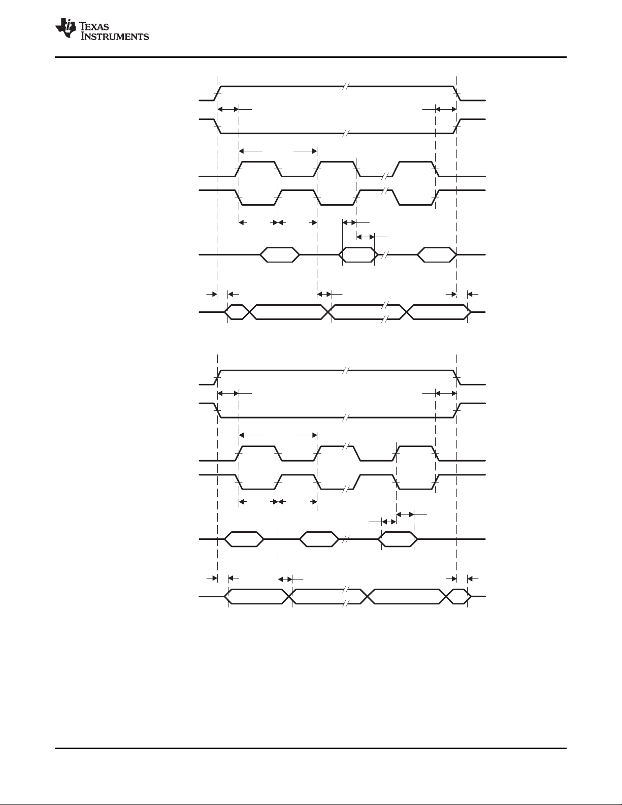
Figure 5-3. SPI Slave Mode, CKPH = 0
Figure 5-4. SPI Slave Mode, CKPH = 1
Copyright © 2012–2014, Texas Instruments Incorporated Specifications 17
Product Folder Links: RF430FRL152H RF430FRL153H RF430FRL154H
Submit Documentation Feedback

SDA
SCL
t
HD,DAT
t
SU,DAT
t
HD,STA
t
HIGH
t
LOW
t
BUF
t
HD,STA
t
SU,STA
t
SP
t
SU,STO
RF430FRL152H, RF430FRL153H, RF430FRL154H
SLAS834C –NOVEMBER 2012–REVISED DECEMBER 2014
www.ti.com
5.15 eUSCI (I2C Mode)
over recommended ranges of supply voltage and operating free-air temperature (unless otherwise noted) (see Figure 5-5)
f
eUSCI
f
SCL
t
HD,STA
t
SU,STA
t
HD,DAT
t
SU,DAT
t
SU,STO
t
SP
t
TIMEOUT
PARAMETER TEST CONDITIONS V
DDB
Internal: SMCLK, ACLK
eUSCI input clock frequency External: UCLK f
Duty cycle = 50% ± 10%
SCL clock frequency 1.5 V 0 400 kHz
f
= 100 kHz 4.0
Hold time (repeated) START 1.5 V µs
Setup time for a repeated START 1.5 V µs
SCL
f
> 100 kHz 0.6
SCL
f
= 100 kHz 4.7
SCL
f
> 100 kHz 0.6
SCL
Data hold time 1.5 V 0 ns
Data setup time 1.5 V 250 ns
f
= 100 kHz 4.0
Setup time for STOP 1.5 V µs
SCL
f
> 100 kHz 0.6
SCL
UCGLITx = 0 50 600 ns
Pulse duration of spikes suppressed by input
filter
UCGLITx = 1 25 300 ns
UCGLITx = 2 12.5 150 ns
1.5 V
UCGLITx = 3 6.25 75 ns
UCCLTOx = 1 27 ms
Clock low time-out UCCLTOx = 2 1.5 V 30 ms
UCCLTOx = 3 33 ms
MIN TYP MAX UNIT
SYSTEM
MHz
Figure 5-5. I2C Mode Timing
5.16 FRAM
over recommended ranges of supply voltage and operating free-air temperature (unless otherwise noted)
PARAMETER TEST CONDITIONS MIN TYP MAX UNIT
t
WRITE
t
Retention
Word or byte write time 125 ns
Read/write endurance 10
15
cycles
Data retention duration TJ= 25°C 10 years
5.17 JTAG
over recommended ranges of supply voltage and operating free-air temperature (unless otherwise noted)
f
TCK
(1) f
PARAMETER V
(1)
TCK input frequency, 4-wire JTAG
may be restricted to meet the timing requirements of the module selected.
TCK
DDB
1.5 V 0 4 MHz
18 Specifications Copyright © 2012–2014, Texas Instruments Incorporated
Submit Documentation Feedback
Product Folder Links: RF430FRL152H RF430FRL153H RF430FRL154H
MIN TYP MAX UNIT

RF430FRL152H, RF430FRL153H, RF430FRL154H
www.ti.com
SLAS834C –NOVEMBER 2012–REVISED DECEMBER 2014
5.18 RFPMM, Power Supply Switch
over recommended ranges of supply voltage and operating free-air temperature (unless otherwise noted)
PARAMETER TEST CONDITIONS MIN TYP MAX UNIT
V
TH+
V
TH-
V
HYST
I
BASVBAT
V
DROP
(1) Battery switch closed. Current = 400 µA
Positive going switching threshold
V
= V
TH+
DDB-VDDR
Negative going switching threshold
V
= V
TH-
DDB-VDDR
Switching voltage hysteresis
V
= V
V
V
HYST
DDB
DROP
TH+-VTH-
input leakage current V
= V
DDB
- V
DDSW
(1)
-60 -35 mV
30 70 110 mV
= 1.65 V, Battery switch open 20 nA
DDB
5.19 RFPMM, Bandgap Reference
over recommended ranges of supply voltage and operating free-air temperature (unless otherwise noted)
PARAMETER TEST CONDITIONS MIN TYP MAX UNIT
V
REF
Output voltage V
= 1.4 V to 1.65 V 892 908 mV
DDSW
5.20 RFPMM, Voltage Doubler
over recommended ranges of supply voltage and operating free-air temperature (unless otherwise noted)
PARAMETER TEST CONDITIONS MIN TYP MAX UNIT
V
V
DD2X
DD2X
Output voltage V
Output voltage V
DDSW
DDSW
= 1.4 V, I
= 1.4 V, I
= 1 µA, cont = 0 V
DD2X
= 100 µA, cont = 1 V
DD2X
2 ×
– mV
DDSW
74mV
2 ×
– mV
DDSW
104mV
35 60 mV
50 mV
5.21 RFPMM, Voltage Supervision
over recommended ranges of supply voltage and operating free-air temperature (unless otherwise noted)
PARAMETER V
V
DDBTH+
V
DDBTH-
V
DDSWTH+
V
DDSWTH-
V
DDDTH+
V
DDDTH-
V
DD2XTH+
V
DD2XTH-
Positive threshold 1.5 V 1.45 V
Negative threshold 1.5 V 1.40 V
Positive threshold 1.40 V
Negative threshold 1.35 V
Positive threshold 1.5 V 1.00 V
Negative threshold 1.5 V 0.90 V
Positive threshold 1.5 V 2.70 V
Negative threshold 1.5 V 2.475 V
DDSW
MIN TYP MAX UNIT
Copyright © 2012–2014, Texas Instruments Incorporated Specifications 19
Submit Documentation Feedback
Product Folder Links: RF430FRL152H RF430FRL153H RF430FRL154H

RF430FRL152H, RF430FRL153H, RF430FRL154H
SLAS834C –NOVEMBER 2012–REVISED DECEMBER 2014
www.ti.com
5.22 SD14, Performance
over recommended ranges of supply voltage and operating free-air temperature (unless otherwise noted)
PARAMETER TEST CONDITIONS MIN NOM MAX UNIT
f
M
Modulator clock frequency 2 kHz
RES Resolution 8 14 Bit
OSR Oversampling ratio 40 2048
B Bandwidth of input signal 1 Hz
V
I
V
offset
V
GErr
∆EG/∆T Gain error temperature coefficient.
E
Unadjusted
t
Start
Input voltage range VI= V
Offset error Complete signal chain -0.75 0.75
Gain error
(2)
(3)
Total unadjusted error -2 2
Startup time 20
(1) FSR = Full Scale Range (SD14 pre-amplifier Gain PGA gain - SD14 gain =1) .
(2) The gain error EGspecifies the deviation of the actual gain G
temperature and supply voltage variations.
(3) Not production tested.
Internal LF oscillator as clock source for
SD14 module
ADCx
- V
SVSS
0 V
REF
FSR
complete signal chain -2% 2%
complete signal chain 100 ppm/K
FSR
cycles
from the nominal gain G
act
: EG= (G
nom
– G
)/G
act
nom
. It covers process,
nom
mV
% of
% of
CLK
(1)
(1)
5.23 SVSS Generator
over recommended ranges of supply voltage and operating free-air temperature (unless otherwise noted)
PARAMETER TEST CONDITIONS MIN TYP MAX UNIT
V
SVSS
t
Settling
Output voltage I
Settling time after switching SVSS on
(95% of final voltage)
= -5uA .. 0uA 80 125 165 mV
SVSS
Switch from VIRTGND = 1 to VIRTGND = 0 400 1000 ms
20 Specifications Copyright © 2012–2014, Texas Instruments Incorporated
Submit Documentation Feedback
Product Folder Links: RF430FRL152H RF430FRL153H RF430FRL154H

RF430FRL152H, RF430FRL153H, RF430FRL154H
www.ti.com
SLAS834C –NOVEMBER 2012–REVISED DECEMBER 2014
5.24 Thermistor Bias Generator
over recommended ranges of supply voltage and operating free-air temperature (unless otherwise noted)
PARAMETER TEST CONDITIONS MIN TYP MAX UNIT
I
OUT,TH
Output current V
= 0 to 0.7 V 2.0 2.4 3.0 µA
OUT
5.25 Temperature Sensor
over recommended ranges of supply voltage and operating free-air temperature (unless otherwise noted)
PARAMETER TEST CONDITIONS MIN TYP MAX UNIT
t
Temperature coefficient 35.7 LSB/K
c
5.26 RF13M, Power Supply and Recommended Operating Conditions
over recommended ranges of supply voltage and operating free-air temperature (unless otherwise noted)
PARAMETER TEST CONDITIONS MIN TYP MAX UNIT
V
DDH
C
IN
Antenna rectified voltage I
= 100 µA 1.8 2 3.6 V
DDH
Input capacitance 2 V RMS 31.5 35 38.5 pF
5.27 RF13M, ISO/IEC 15693 ASK Demodulator
over recommended ranges of supply voltage and operating free-air temperature (unless otherwise noted)
PARAMETER MIN TYP MAX UNIT
DR
100
m100 Modulation depth 100%, test as defined in ISO10373 90% 100%
m10 Modulation depth 10%, test as defined in ISO10373 7% 30%
|t
PLH
t
, t
PLH
t
pd100
t
D100
Input signal data rate 100% downlink modulation, 100% ASK, ISO/IEC 15693 6 26 kbps
– t
| Delta propagation delay of RXD_10 to V
PHL
Propagation delay of RXD_10 to V
PHL
IN
IN
0 2.35 µs
0 7.07 µs
Propagation delay of RXD_100 7.07 µs
Minimum pulse duration of RxD_100 5 µs
5.28 RF13M, ISO/IEC 15693 Compliant Load Modulator
over recommended ranges of supply voltage and operating free-air temperature (unless otherwise noted)
PARAMETER MIN TYP MAX UNIT
f
PICC
V
A_MOD
V
SUB15
Uplink subcarrier modulation frequency 0.2 1 MHz
Modulated antenna voltage, V
= 2,3V 0.5 V
A_unmod
Uplink modulation subcarrier level, ISO/IEC 15693 10 mV
Copyright © 2012–2014, Texas Instruments Incorporated Specifications 21
Submit Documentation Feedback
Product Folder Links: RF430FRL152H RF430FRL153H RF430FRL154H

RF430FRL152H, RF430FRL153H, RF430FRL154H
SLAS834C –NOVEMBER 2012–REVISED DECEMBER 2014
6 Detailed Description
6.1 CPU
The MSP430 CPU has a 16-Bit RISC architecture that is highly transparent to the application. All
operations, other than program-flow instructions, are performed as register operations in conjunction with
seven addressing modes for source operand and four addressing modes for destination operand.
The CPU is integrated with 16 registers that provide reduced instruction execution time. The register-toregister operation execution time is one cycle of the CPU clock.
Four of the registers, R0 to R3, are dedicated as program counter, stack pointer, status register, and
constant generator respectively. The remaining registers are general-purpose registers.
Peripherals are connected to the CPU using data, address, and control buses, and can be handled with all
instructions.
6.2 Instruction Set
The instruction set consists of the original 51 instructions with three formats and seven address modes.
Each instruction can operate on word and byte data.
www.ti.com
22 Detailed Description Copyright © 2012–2014, Texas Instruments Incorporated
Submit Documentation Feedback
Product Folder Links: RF430FRL152H RF430FRL153H RF430FRL154H

www.ti.com
6.3 Operating Modes
The device has one active mode and three software selectable low-power modes of operation. An
interrupt event can wake up the device from any of the three low-power modes, service the request, and
restore back to the low-power mode on return from the interrupt program.
The software-selected low-power mode might not be reached if at least one module still
requests a clock on MCLK, SMCLK, or ACLK. The CPU, however, remains off until an
interrupt occurs.
The following operating modes can be configured by software:
• Active mode AM
– CPU is enabled
– All clocks are active.
• Low-power mode 0 (LPM0)
– CPU is disabled
– MCLK is disabled
– SMCLK is active
– ACLK is active
– HFOSC is off, if not selected for SMCLK or ACLK
• Low-power mode 3 (LPM3)
– CPU is disabled
– MCLK is disabled
– SMCLK is disabled
– ACLK is active
– HFOSC is off, if not selected for ACLK
• Low-power mode 4 (LPM4)
– CPU is disabled
– MCLK is disabled
– SMCLK is disabled
– ACLK is disabled
– HFOSC is off, LFOSC is on
RF430FRL152H, RF430FRL153H, RF430FRL154H
SLAS834C –NOVEMBER 2012–REVISED DECEMBER 2014
NOTE
LPM1 is identical to LPM0, and LPM2 is identical to LPM3, because the SCG0 bit has no influence on
HFOSC.
Copyright © 2012–2014, Texas Instruments Incorporated Detailed Description 23
Submit Documentation Feedback
Product Folder Links: RF430FRL152H RF430FRL153H RF430FRL154H

RF430FRL152H, RF430FRL153H, RF430FRL154H
SLAS834C –NOVEMBER 2012–REVISED DECEMBER 2014
6.4 Interrupt Vector Addresses
The interrupt vectors and the power-up start address are located in the address range 0FFFFh to 0FFE0h.
Address Range 0FFDFh to 0FFD0h is reserved for bootcode signatures. The vector contains the 16-bit
address of the appropriate interrupt-handler instruction sequence.
Table 6-1. Interrupt Sources, Flags, and Vectors
www.ti.com
INTERRUPT SOURCE INTERRUPT FLAG PRIORITY
SYSTEM WORD
INTERRUPT ADDRESS
System Reset
Power-Up
WDTIFG
(1)
Reset FFFEh 15, highest
External Reset
Watchdog
System NMI
SVMIFG, VMAIFG
(1)
(Non)maskable 0FFFCh 14
Vacant memory access
User NMI
NMIIFG
(1)(2)
(Non)maskable 0FFFAh 13
NMI
TimerA0_A3 TA0CCR0 CCIFG0
(3)
Maskable 0FFF8h 12
TA0CCR1 CCIFG1
TimerA0_A3 TA0CCR2 CCIFG2 Maskable 0FFF6h 11
TA0CTL TAIFGTA0IV
Watchdog,
Interval Timer Mode
WDTIFG Maskable 0FFF4h 10
(1)(3)
RF13MRXIFG, RF13MTXIFG, RF13MRXWMIFG,
RF13M Module Maskable 0FFF2h 9
RF13MTXWMIFG, RF13MSLIFG,
RF13MOUFLIFG, RF13MRXEIFG,
RF13MIVx
(1)(3)
(SPI mode)
UCB0RXIFG, UCB0TXIFG
(I2C mode)
UCB0ALIFG, UCB0NACKIFG, UCB0STTIFG,
eUSCIB UCB0STPIFG, UCB0RXIFG3, UCB0TXIFG3, Maskable 0FFF0h 8
UCB0RXIFG2, UCB0TXIFG2, UCB0RXIFG1,
UCB0TXIFG1, UCB0RXIFG0, UCB0TXIFG0,
UCB0CNTIFG, UCB0CLTOIFG, UCB0BIT9IFG
(SD14IV)
Sigma Delta ADC SD14OVIFG, SD14IFG
I/O Port P1 Maskable 0FFECh 6
RFPMM Maskable 0FFEAh 5
RFPMMIFGV2X, RFPMMIFGVH, RFPMMIFGVR,
(1)(3)
(1)(3)
P1IFG.0 to P1IFG.7
(P1IV)
(1)(3)
RFPMMIFGVB, RFPMMIFGVF, RFPMMIV
Maskable 0FFEEh 7
0FFE8h 4
Reserved Reserved
(4)
⋮ ⋮
0FFDCh 0
(1) Multiple source flags
(2) A reset is generated if the CPU tries to fetch instructions from within peripheral space or vacant memory space.
(Non)maskable: the individual interrupt-enable bit can disable an interrupt event, but the general-interrupt enable cannot disable it.
(3) Interrupt flags are located in the module.
(4) Reserved interrupt vectors at these addresses are not used in this device and can be used for regular program code if necessary. To
maintain compatibility with other devices, it is recommended to reserve these locations.
24 Detailed Description Copyright © 2012–2014, Texas Instruments Incorporated
Submit Documentation Feedback
Product Folder Links: RF430FRL152H RF430FRL153H RF430FRL154H

RF430FRL152H, RF430FRL153H, RF430FRL154H
www.ti.com
SLAS834C –NOVEMBER 2012–REVISED DECEMBER 2014
Table 6-1. Interrupt Sources, Flags, and Vectors (continued)
INTERRUPT SOURCE INTERRUPT FLAG PRIORITY
CRC Value 0FFDAh
CRC Length 0FFD8h
Signatures
Loader Signature 1 0FFD6h
Loader Signature 0 0FFD4h
JTAG Signature 1 0FFD2h
JTAG Signature 0 0FFD0h
SYSTEM WORD
INTERRUPT ADDRESS
Copyright © 2012–2014, Texas Instruments Incorporated Detailed Description 25
Submit Documentation Feedback
Product Folder Links: RF430FRL152H RF430FRL153H RF430FRL154H

RF430FRL152H, RF430FRL153H, RF430FRL154H
SLAS834C –NOVEMBER 2012–REVISED DECEMBER 2014
6.5 Memory
Table 6-2 shows the memory organization of the devices.
Table 6-2. Memory Map RF430FRL152H, RF430FRL153H, RF430FRL154H
www.ti.com
TYPE RF430FRL152H RF430FRL152H
Memory (FRAM) Total Size 2048 B = 2 KB
Main: interrupt vector FRAM 0FFFFh-0FFE0h
Main: Code Memory Bank A
Boot Data (TLV) Size 64 B 64 B
Application ROM Size 7168 B = 7 KB 3584 B = 3.5 KB
ROM Development Memory Size - 3584 B = 3.5 KB
SRAM Memory Size 4096 B = 4 KB 512 B = 0.5 KB
Peripherals Size 4096 B = 4 KB 4096 B = 4 KB
(1) Write protectable. See also Table 6-3
(2) Address range includes interrupt vector.
(1)(2)
(1)
Bank B
(1)
Bank C
Bank D 448 B
FRAM 01A3Fh-01A00h 01A3Fh-01A00h
ROM 05FFFh-04400h 051FFh-04400h
SRAM - 02BFFh-01E00h
SRAM 02BFFh-01C00h 01DFFh-01C00h
RF430FRL153H RF430FRL153H
RF430FRL154H RF430FRL154H
Normal Mode ROM Development Mode
512 B
0FFFFh-0FE00h
512 B
0FDFFh-0FC00h
512 B
0FBFFh-0FA00h
0F9FFh-0F840h
00FFFh-00000h 00FFFh-00000h
6.5.1 FRAM
The FRAM can be programmed through the JTAG port or in-system by the CPU, data are received
through RF, SPI or I2C Sensor Interface.
Features of the FRAM include:
• Low-power ultra-fast-write non-volatile memory
• Byte and word access capability
• Automated wait state generation
The following address ranges can be write protected by setting the corresponding bit in the SYSCNF
register, see the RF430FRL15xH Family Technical Reference Manual (SLAU506).
Table 6-3. Write Protectable FRAM Address Ranges
BIT Address Range
FRAMLCK2
FRAMLCK1
FRAMLCK0
512 B
0FFFFh-0FE00h
512 B
0FDFFh-0FC00h
512 B
0FBFFh-0FA00h
26 Detailed Description Copyright © 2012–2014, Texas Instruments Incorporated
Submit Documentation Feedback
Product Folder Links: RF430FRL152H RF430FRL153H RF430FRL154H

www.ti.com
6.5.2 SRAM
The SRAM memory is made up of 8 sectors. Each sector can be completely powered down to save
leakage; however, all data is lost. Features of the SRAM memory include:
• SRAM memory has 8 sectors of 512 B each.
• Each sector 0 to 8 can be complete disabled; however, data retention is lost.
• Each sector 0 to 8 automatically enters low-power retention mode when possible.
6.5.3 Application ROM
The Application ROM consists of four parts. The RF Library provides ISO/IEC 15693 functions necessary
for operating the 13.65 MHz front end. The Function library holds the device and memory function used by
the boot code and RF library. These functions are user accessible. The ROM contains the predefined
application FW. The boot code checks the password and releases control to the application or enables
JTAG on password match, enters LPM4 and waits for debug session, see the RF430FRL15xH Firmware
User's Guide (SLAU603).
6.6 Peripherals
Peripherals are connected to the CPU through data, address, and control buses. All peripherals can be
managed using all instructions. For complete module descriptions, see the RF430FRL15xH Family
Technical Reference Manual (SLAU506).
RF430FRL152H, RF430FRL153H, RF430FRL154H
SLAS834C –NOVEMBER 2012–REVISED DECEMBER 2014
6.6.1 Digital I/O, (P1.x)
There is one I/O port implemented, P1, with eight I/O lines RF430FRL15xH.
• All individual I/O bits are independently programmable.
• Any combination of input, output, and interrupt conditions is possible.
• Programmable pullup or pulldown resistor on all ports.
• Edge-selectable interrupt input capability for all ports on P1.
• Read and write access to port-control registers is supported by all instructions.
6.6.2 Versatile I/O Port P1
The versatile I/O ports P1 feature device dependent reset values. The reset values for the
RF430FRL15xH devices are shown in Table 6-4.
Table 6-4. Versatile Port Reset Values
PORT
NUMBER
P1.0 0 0 0 0 0 PUC yes P1.0, input
P1.1 0 0 0 0 0 PUC yes P1.1, input
P1.2 0 0 0 0 0 PUC yes P1.2, input
P1.3 0 0 0 0 0 PUC yes P1.3, input
P1.4 1 0 1 1 1 PUC yes JTAG TCK, P1.4, input
P1.5 1 0 1 1 1 PUC yes JTAG TDI, P1.5, input
P1.6 0 0 0 1 1 PUC yes JTAG TDO, P1.6, output
P1.7 1 0 1 1 1 PUC yes JTAG TMS, P1.7, input
PxOUT PxDIR PxREN PxSEL0 PxSEL1 RESET PORTS ON COMMENT
6.6.3 Oscillator and System Clock
The clock system in the RF430FRL15xH devices is supported by the Compact Clock System (CCS)
module that includes support for an internal trimmable 256-kHz current-controlled low-frequency oscillator
(LFOSC) and an internal 4-MHz current-controlled high-frequency oscillator (HFOSC).
Copyright © 2012–2014, Texas Instruments Incorporated Detailed Description 27
Submit Documentation Feedback
Product Folder Links: RF430FRL152H RF430FRL153H RF430FRL154H

RF430FRL152H, RF430FRL153H, RF430FRL154H
SLAS834C –NOVEMBER 2012–REVISED DECEMBER 2014
The CCS module is designed to meet the requirements of both low system cost and low power
consumption. The CCS provides a fast turn-on of the oscillators in less than 1 ms. The CCS module
provides the following clock signals:
• Auxiliary clock (ACLK), sourced from the 256-kHz internal LFOSC.
• Main clock (MCLK), the system clock used by the CPU. MCLK can be sourced by same sources made
available to ACLK.
• Sub-Main clock (SMCLK), the subsystem clock used by the peripheral modules. SMCLK can be
sourced by same sources made available to ACLK.
6.6.4 Compact System Module (C-SYS_A)
The Compact SYS module handles many of the system functions within the device. These include poweron reset and power-up clear handling, NMI source selection and management, reset interrupt vector
generators, as well as, configuration management. It also includes a data exchange mechanism through
JTAG called a JTAG mailbox that can be used in the application.
Table 6-5. System Module Interrupt Vector Registers
www.ti.com
INTERRUPT VECTOR
REGISTER
SYSRSTIV, System Reset No interrupt pending 019Eh 00h
SYSSNIV, System NMI No interrupt pending 019Ch 00h
SYSUNIV, User NMI No interrupt pending 019Ah 00h
SYSBERRIV, Bus Error No interrupt pending 0198h 00h
INTERRUPT VECTOR WORD ADDRESS OFFSET PRIORITY
Brownout (BOR) 02h Highest
SVMBOR (BOR) 04h
RST/NMI (BOR) 06h
DoBOR (BOR) 08h
Security violation (BOR) 0Ah
DoPOR (POR) 0Ch
WDT time-out (PUC) 0Eh
WDT key violation (PUC) 10h
CCS key violation 12h
PMM key violation 14h
Peripheral area fetch (PUC) 16h
Reserved 18h-3Eh Lowest
SVMIFG 02h Highest
VMAIFG 04h
JMBINIFG 06h
JMBOUTIFG 08h
Reserved 0Ah-3Eh Lowest
NMIFG 02h Highest
OFIFG 04h
BERR 06h
Reserved 08h-3Eh Lowest
Reserved 02h-3Eh Lowest
6.6.5 Watchdog Timer (WDT_A)
The primary function of the watchdog timer (WDT_A) module is to perform a controlled system restart
after a software problem occurs. If the selected time interval expires, a system reset is generated. If the
watchdog function is not needed in an application, the module can be configured as an interval timer and
can generate interrupts at selected time intervals.
28 Detailed Description Copyright © 2012–2014, Texas Instruments Incorporated
Submit Documentation Feedback
Product Folder Links: RF430FRL152H RF430FRL153H RF430FRL154H

www.ti.com
6.6.6 Reset, NMI, SVMOUT System
The reset system of the RF430FRL15xH devices features the function reset input, reset output, and NMI
input.
6.6.7 Timer_A (Timer0_A3)
Timer_A is a 16-bit timer/counter with three capture/compare registers. Timer_A can support multiple
capture/compares, PWM outputs, and interval timing. Timer_A also has extensive interrupt capabilities.
Interrupts may be generated from the counter on overflow conditions and from each of the
capture/compare registers.
Table 6-6. Timer0_A3 Signal Connections
RF430FRL152H, RF430FRL153H, RF430FRL154H
SLAS834C –NOVEMBER 2012–REVISED DECEMBER 2014
INPUT PIN DEVICE INPUT MODUL INPUT MODULE DEVICE OUTPUT OUTPUT PIN
NUMBER SIGNAL SIGNAL OUTPUT SIGNAL SIGNAL NUMBER
8 – P1.3 TA0CLK TACLK
ACLK (internal) ACLK
SMCLK (internal) SMCLK
TA0CLK TACLK
12 – P1.0 TA0.0 CCI0A 9 – P1.2
11 – P1.1 TA0.0 CCI0B 20 – P1.6
V
SS
V
DDB
22 – P1.4 TA0.1 CCI1A 12 – P1.0
21 – P1.5 TA0.1 CCI1B 22 – P1.4
V
SS
V
DDB
20 – P1.6 TA0.2 CCI2A 11 – P1.1
19 – P1.7 TA0.2 CCI2B 8 – P1.3
V
SS
V
DDB
GND 19 – P1.7
Vcc
GND 19 – P1.7
Vcc
GND 21 – P1.5
Vcc 20 – P1.6
MODULE BLOCK
Timer NA NA
CCR0 TA0 TA0.0
CCR1 TA1 TA0.1
CCR2 TA2 TA0.2
6.6.8 Enhanced Universal Serial Communication Interface (eUSCI_B0)
The eUSCI_B0 module is used for serial data communication. The eUSCI module supports synchronous
communication protocols such as SPI (3 pin or 4 pin) and I2C.
The eUSCI_B0 module provides support for SPI (3 pin or 4 pin) or I2C.
6.6.9 ISO/IEC 15693 Analog Front End (RF13M)
The ISO/IEC 15693 module supports contact-less communication over the analog front end according to
ISO/IEC 15693 with data rates up to 26.48 kbps for receive and 26.48 kbps for transmit. It includes
decode of receive data and encode of transmit data, both synchronous with the AFE carrier clock.
6.6.10 ISO/IEC 15693 Decoder/Encoder (RF13M)
The module interfaces directly to the analog front end to ensure correct timing for transmit and receive of
data derived from the 13.56-MHz carrier frequency.
6.6.11 CRC16 Module (CRC16)
The CRC16 module produces a signature based on a sequence of entered data values and can be used
for data
checking purposes. The CRC16 module is compliant with ISO/IEC 13239, it is 16 bits long, polynominal is:
x16+ x12+ x5+ 1, direction is backward, and preset is 0xFFFF. For more information see ISO/IEC 13239.
Copyright © 2012–2014, Texas Instruments Incorporated Detailed Description 29
Submit Documentation Feedback
Product Folder Links: RF430FRL152H RF430FRL153H RF430FRL154H

RF430FRL152H, RF430FRL153H, RF430FRL154H
SLAS834C –NOVEMBER 2012–REVISED DECEMBER 2014
6.6.12 14-Bit Sigma-Delta ADC (SD14)
A sigma-delta modulator is provided for high resolution analog-to-digital conversion of quasi-dc voltages:
• First-order integrator, 1-bit comparator, 1-bit DAC
• Sampling frequency of up to 2 kHz
• Fully differential
6.6.13 Programmable Gain Amplifier (SD14)
The PGA features a very high-impedance input and a programmable gain combined with full offset
compensation, very low offset drift, and low noise.
6.6.14 Peripheral Register Map
Table 6-7. Peripheral Register Map
www.ti.com
MODULE NAME REGISTER DESCRIPTION REGISTER OFFSET
RF13M RF13M RX/TX High/Low Watermark Configuration Register RF13MWMCFG 0800h 0Eh
RF13M RX/TX FIFO Fill Level register RF13MFIFOFL 0Ch
RF13M CRC accumulator Register RF13MCRC 0Ah
RF13M Transmit Data FIFO Register RF13MTXF 08h
RF13M Receive Data FIFO Register RF13MRXF 06h
RF13M Interrupt Vector Register RF13MIV 04h
RF13M Interrupt Register RF13MINT 02h
RF13M Control Register RF13MCTL 00h
SD14 SD14 Interrupt Vector Register SD14IV 0700h 0Ch
SD14 Intermediate Conversion Result Register SD14MEM3 0Ah
SD14 Intermediate Conversion Result Register SD14MEM2 08h
SD14 Intermediate Conversion Result Register SD14MEM1 06h
SD14 Conversion Result SD14MEM0 04h
SD14 Control Register 1 SD14CTL1 02h
SD14 Control Register 0 SD14CTL0 00h
eUSCI_B0 Interrupt Vector Word Register UCB0IV 0640h 2Eh
Interrupt Flags Register UCB0IFG 2Ch
Interrupt Enable Register UCB0IE 2Ah
I2C Slave Address Register UCB0I2CSA 20h
Address Mask Register UCB0ADDMASK 1Eh
Received Address Register UCB0ADDRX 1Ch
I2C Own Address 3 Register UCB0I2COA3 1Ah
I2C Own Address 2 Register UCB0I2COA2 18h
I2C Own Address 1 Register UCB0I2COA1 16h
I2C Own Address 0 Register UCB0I2COA0 14h
Transmit Buffer Register UCB0TXBUF 0Eh
Receive Buffer Register UCB0RXBUF 0Ch
Byte Counter Threshold Register UCB0TBCNT 0Ah
Status Word Register UCB0STATW 08h
Bit Rate 1 Register UCB0BR1 07h
Bit Rate 0 Register UCB0BR0 06h
Control Word 1 Register UCB0CTLW1 02h
Control Word 0 Register UCB0CTLW0 00h
BASE
ADDRESS
30 Detailed Description Copyright © 2012–2014, Texas Instruments Incorporated
Submit Documentation Feedback
Product Folder Links: RF430FRL152H RF430FRL153H RF430FRL154H

RF430FRL152H, RF430FRL153H, RF430FRL154H
www.ti.com
SLAS834C –NOVEMBER 2012–REVISED DECEMBER 2014
Table 6-7. Peripheral Register Map (continued)
MODULE NAME REGISTER DESCRIPTION REGISTER OFFSET
Timer0_A3 Timer0_A Interrupt Vector Register TA0IV 0340h 2Eh
Capture/Compare Register 2 TA0CCR2 16h
Capture/Compare Register 1 TA0CCR1 14h
Capture/Compare Register 0 TA0CCR0 12h
Timer0_A Counter Register TA0R 10h
Capture/Compare Control 2 Register TA0CCTL2 06h
Capture/Compare Control 1 Register TA0CCTL1 04h
Capture/Compare Control 0 Register TA0CCTL0 02h
Timer0_A Control Register TA0CTL 00h
Port P1 Port P1 Interrupt Flag Register P1IFG 0200h 1Ch
Port P1 Interrupt Enable Register P1IE 1Ah
Port P1 Interrupt Edge Select Register P1IES 18h
Port P1 Interrupt Vector Word Register P1IV 0Eh
Port P1 Selection 1 Register P1SEL1 0Ch
Port P1 Selection 0 Register P1SEL0 0Ah
Port P1 Pullup/Pulldown Enable Register P1REN 06h
Port P1 Direction Register P1DIR 04h
Port P1 Outout Register P1OUT 02h
Port P1 Input Register P1IN 00h
CSYS_A Reset Vector Generator Register SYSRSTIV 0180h 1Eh
System NMI Vector Generator Register SYSSNIV 1Ch
User NMI Vector Generator Register SYSUNIV 1Ah
Bus Error Vector Generator Register SYSBERRIV 18h
System Configuration Actuator 0 Register SYSCA0 14h
System Configuration Register SYSCNF 10h
JTAG Mailbox Output Register 1 SYSJMBO1 0Eh
JTAG Mailbox Output Register 0 SYSJMBO0 0Ch
JTAG Mailbox Input Register 1 SYSJMBI1 0Ah
JTAG Mailbox Input Register 0 SYSJMBI0 08h
JTAG Mailbox Control Register SYSJMBC 06h
System Control Register SYSCTL 00h
CCS CCS Control 8 Register CCSCTL8 0160h 10h
CCS Control 7 Register CCSCTL7 0Eh
CCS Control 6Register CCSCTL6 0Ch
CCS Control 5 Register CCSCTL5 0Ah
CCS Control 4 Register CCSCTL4 08h
CCS Control 1 Register CCSCTL1 02h
CCS Control 0 Register CCSCTL0 00h
WDT_A, CRC Watchdog Timer Control Register WDTCTL 0150h 0Ch
CRC Result Reverse Register CRCRESR 06h
CRC Initialization and Result Register CRCINIRES 04h
CRC Data In Reverse Byte Register CRCDIRB 02h
CRC Data In Register CRCDI 00h
FRAM Control General Control 1 Register GCCTL1 0140h 06h
General Control 0 Register GCCTL0 04h
FRAM Control 0 Register FRCTL0 00h
BASE
ADDRESS
Copyright © 2012–2014, Texas Instruments Incorporated Detailed Description 31
Submit Documentation Feedback
Product Folder Links: RF430FRL152H RF430FRL153H RF430FRL154H

RF430FRL152H, RF430FRL153H, RF430FRL154H
SLAS834C –NOVEMBER 2012–REVISED DECEMBER 2014
www.ti.com
Table 6-7. Peripheral Register Map (continued)
MODULE NAME REGISTER DESCRIPTION REGISTER OFFSET
RFPMM RFPMM Interrupt Vector Register RFPMMIV 0120h 08h
RFPMM Interrupt Flag Register RFPMMIFG 06h
RFPMM Interrupt Enable Register RFPMMIE 04h
RFPMM Control Register 1 RFPMMCTL1 02h
RFPMM Control Register 0 RFPMMCTL0 00h
Special Functions SFR Reset Pin Control Register SFRRPCR 0100h 04h
SFR Interrupt Flag Register SFRIFG1 02h
SFR Interrupt Enable Register SFRIE1 00h
BASE
ADDRESS
32 Detailed Description Copyright © 2012–2014, Texas Instruments Incorporated
Submit Documentation Feedback
Product Folder Links: RF430FRL152H RF430FRL153H RF430FRL154H

P1REN.x
00
01
10
11
P1DIR.x
00
01
10
11
P1OUT.x
TA0.1
SPI_SIMO/SDA
SMCLK
P1SEL0.x
P1SEL1.x
0
1Vcc
Vss
P1IN.x
EN1
EN2
DModul x IN
#
Pad Logic
P1.0/SPI_SIMO/SDA/SMCLK /TA0 .1/CCI 0.0
PortsOn
P1IRQ.x
P1IE.x
P1IES.x Set
Q
P1IFG.x
eUSCI_B0
Bus
Keeper
www.ti.com
6.7 Port Schematics
6.7.1 Port P1.0 Input/Output
RF430FRL152H, RF430FRL153H, RF430FRL154H
SLAS834C –NOVEMBER 2012–REVISED DECEMBER 2014
(1) X = Don't care
(2) Module controls direction of port, depending on whether RF430 device is master or slave.
Copyright © 2012–2014, Texas Instruments Incorporated Detailed Description 33
Table 6-8. Port P1.0 Pin Functions
CONTROL BITS OR SIGNALS
PIN NAME (P1.x) x FUNCTION
P1.0/SPI_SIMO/SDA/SMCLK/TA0.1/CCI0.0 0 SMCLK 1 1 0 0
P1.0 (I/O) I:0; O:1 0 0 0
SPI_SIMO/SDA
TA0.1 1 1 1 0
Timer A0, CCI0A 0 ≠0 ≠0 X
(2)
P1DIR.x P1SEL1.x P1SEL0.x
1 0 1 0
(1)
RSELx/
ASELx
Submit Documentation Feedback
Product Folder Links: RF430FRL152H RF430FRL153H RF430FRL154H

P1REN.x
00
01
10
11
P1DIR.x
00
01
10
11
P1OUT.x
TA0.2
SPI_SOMI/SCL
ACLK
P1SEL0.x
P1SEL1.x
0
1Vcc
Vss
P1IN.x
EN1
EN2
DModul x IN
#
Pad Logic
P1.1/SPI_SOMI/SCL/ACLK/TA0.2/CCI0.0
PortsOn
P1IRQ.x
P1IE.x
P1IES.x Set
Q
P1IFG.x
eUSCI_B0
Bus
Keeper
RF430FRL152H, RF430FRL153H, RF430FRL154H
SLAS834C –NOVEMBER 2012–REVISED DECEMBER 2014
6.7.2 Port P1.1 Input/Output
www.ti.com
(1) X = Don't care
(2) Module controls direction of port, depending on whether RF430 device is master or slave.
34 Detailed Description Copyright © 2012–2014, Texas Instruments Incorporated
Table 6-9. Port P1.1 Pin Functions
CONTROL BITS OR SIGNALS
1 0 1 0
P1DIR.x P1SEL1.x P1SEL0.x
P1.1 (I/O) I:0; O:1 0 0 0
SPI_SOMI/SCL
TA0.2 1 1 1 0
Timer A1, CCI0B 0 ≠0 ≠0 X
(2)
PIN NAME (P1.x) x FUNCTION
P1.1/SPI_SOMI/SCL/ACLK/TA0.2/CCI0.0 1 ACLK 1 1 0 0
Submit Documentation Feedback
Product Folder Links: RF430FRL152H RF430FRL153H RF430FRL154H
(1)
RSELx/ASE
Lx

P1REN.x
00
01
10
11
P1DIR.x
00
01
10
11
P1OUT.x
TA0.0
SPI_CLK
MCLK
P1SEL0.x
P1SEL1.x
0
1Vcc
Vss
P1IN.x
EN1
EN2
DModul x IN
#
Pad Logic
P1.2/SPI_CLK/MCLK/TA0.0
PortsOn
P1IRQ.x
P1IE.x
P1IES.x Set
Q
P1IFG.x
eUSCI_B0
Bus
Keeper
www.ti.com
6.7.3 Port P1.2 Input/Output
RF430FRL152H, RF430FRL153H, RF430FRL154H
SLAS834C –NOVEMBER 2012–REVISED DECEMBER 2014
P1.2/SPI_CLK/MCLK/TA0.0 2
(1) X = Don't care
(2) Module controls direction of port, depending on whether RF430 device is master or slave.
Copyright © 2012–2014, Texas Instruments Incorporated Detailed Description 35
Table 6-10. Port P1 (P1.2) Pin Functions
PIN NAME (P1.x) x FUNCTION
P1.2 (I/O) I:0; O:1 0 0 0
SPI_CLK
MCLK 1 1 0 0
TA0.0 1 1 1 0
(2)
Submit Documentation Feedback
Product Folder Links: RF430FRL152H RF430FRL153H RF430FRL154H
CONTROL BITS OR SIGNALS
P1DIR.x P1SEL1.x P1SEL0.x
1 0 1 0
(1)
RSELx/ASEL
x

P1REN.x
00
01
10
11
P1DIR.x
00
01
10
11
P1OUT.x
SPI_STE
TA0.2
P1SEL0.x
P1SEL1.x
0
1Vcc
Vss
P1IN.x
EN1
EN2
DModul x IN
#
Pad Logic
P1.3/SPI_STE/TA0.2/ACLK/TA0CLK
PortsOn
P1IRQ.x
P1IES.x Set
Q
P1IFG.x
eUSCI_B0
Bus
Keeper
RF430FRL152H, RF430FRL153H, RF430FRL154H
SLAS834C –NOVEMBER 2012–REVISED DECEMBER 2014
6.7.4 Port P1.3 Input/Output
www.ti.com
P1.3/SPI_STE/TA0.2/ACLK/TA0CLK 3 TA0.2 1 1 0 0
(1) X = Don't care
(2) Module controls direction of port, depending on whether RF430 device is master or slave.
36 Detailed Description Copyright © 2012–2014, Texas Instruments Incorporated
PIN NAME (P1.x) x FUNCTION
Table 6-11. Port P1 (P1.3) Pin Functions
P1.3 (I/O) I:0; O:1 0 0 0
SPI_STE
ACLK 1 1 1 0
TA0CLK X ≠0 ≠0 X
Submit Documentation Feedback
Product Folder Links: RF430FRL152H RF430FRL153H RF430FRL154H
CONTROL BITS OR SIGNALS
P1DIR.x P1SEL1.x P1SEL0.x
(2)
1 0 1 0
(1)
RSELx/ASE
Lx

P1REN.x
00
01
10
11
P1DIR.x
00
01
10
11
P1OUT.x
RFU
TA0.1
SMCLK
P1SEL0.x
P1SEL1.x
0
1Vcc
Vss
P1IN.x
EN1
EN2
DModule X IN
#
Pad Logic
P1.4/TA0.1/SMCLK/TCK /CCI0.1/CLKIN
TCK to JTAG logic
PortsOn
P1IRQ.x
P1IES.x Set
Q
P1IFG.x
Bus
Keeper
Pad Logic
to clock system
www.ti.com
6.7.5 Port P1.4 Input/Output
RF430FRL152H, RF430FRL153H, RF430FRL154H
SLAS834C –NOVEMBER 2012–REVISED DECEMBER 2014
TCK/P1.4/TA0.1/SMCLK/CCI0.1 4 Reserved 1 1 1 0
(1) X = Don't care
(2) JTAG signals TMS, TCK, and TDI read as 1 when not configured as explicit JTAG terminals.
(3) JTAG overrides digital output control when configured as explicit JTAG terminals.
(4) JTAG function with enabled pullup resistors is default after power up.
PIN NAME (P1.x) x FUNCTION
Table 6-12. Port P1.4 Pin Functions
P1.4 (I/O) I:0; O:1 0 0 0
Timer_A0.1 1 0 1 0
SMCLK 1 1 0 0
Timer_A0.CCI1A 0 ≠0 ≠0 0
JTAG-TCK
CLKIN from bypass X X X 0
(2)(3)(4)
CONTROL BITS OR SIGNALS
P1DIR.x P1SEL1.x P1SEL0.x JTAG Mode
X X X 1
(1)
Copyright © 2012–2014, Texas Instruments Incorporated Detailed Description 37
Product Folder Links: RF430FRL152H RF430FRL153H RF430FRL154H
Submit Documentation Feedback

P1REN.x
00
01
10
11
P1DIR.x
00
01
10
11
P1OUT.x
RFU
TA 0.2
MCLK
P1SEL0.x
P1SEL1.x
0
1Vcc
Vss
P1IN.x
EN1
EN2
DModule X IN
#
Pad Logic
P1.5/TA0.2/MCLK/TDI/CCI0.1
TDI to JTAG logic
PortsOn
P1IRQ.x
P1IE.x
P1IES.x Set
Q
P1IFG.x
Bus
Keeper
RF430FRL152H, RF430FRL153H, RF430FRL154H
SLAS834C –NOVEMBER 2012–REVISED DECEMBER 2014
6.7.6 Port P1.5 Input/Output
www.ti.com
Table 6-13. Port P1.5 Pin Functions
PIN NAME (P1.x) x FUNCTION
TDI/P1.5/TA0.2/MCLK/CCI0.1 5
(1) X = Don't care
(2) JTAG signals TMS, TCK, and TDI read as 1 when not configured as explicit JTAG terminals.
(3) JTAG overrides digital output control when configured as explicit JTAG terminals.
(4) JTAG function with enabled pullup resistors is default after power up.
P1.5 (I/O) I:0; O:1 0 0 0
Timer_A0.2 1 0 1 0
MCLK 1 1 0 0
Timer_A0 CCI1B 0 ≠0 ≠0 0
JTAG-TDI
(2)(3)(4)
P1DIR.x P1SEL1.x P1SEL0.x JTAG Mode
CONTROL BITS OR SIGNALS
1 1 1 0
X X X 1
(1)
38 Detailed Description Copyright © 2012–2014, Texas Instruments Incorporated
Product Folder Links: RF430FRL152H RF430FRL153H RF430FRL154H
Submit Documentation Feedback

P1REN.x
00
01
10
11
P1DIR.x
00
01
10
11
P1OUT.x
TDO from JTAG
TA0.0
TA0.2
P1SEL0.x
P1SEL1.x
0
1Vcc
Vss
P1IN.x
EN1
EN2
DModule X IN
#
Pad Logic
TDO/P1.6/TA0.0/TA0.2/CCI0.2
from JTAG logic
PortsOn
P1IRQ.x
P1IE.x
P1IES.x
Set
Q
P1IFG.x
Bus
Keeper
www.ti.com
6.7.7 Port P1.6 Input/Output
RF430FRL152H, RF430FRL153H, RF430FRL154H
SLAS834C –NOVEMBER 2012–REVISED DECEMBER 2014
TDO/P1.6/TA0.0/TA0.2/CCI0.2 6 Timer_A0.2 1 1 0
(1) JTAG signals TMS, TCK, and TDI read as 1 when not configured as explicit JTAG terminals.
(2) JTAG overrides digital output control when configured as explicit JTAG terminals.
Table 6-14. Port P1.6 Pin Functions
PIN NAME (P1.x) x FUNCTION
P1.6 (I/O) I:0; O:1 0 0
Timer_A0.0 1 0 1
JTAG-TDO
Timer_A0 CCI2A 0 ≠0 ≠0
(1)(2)
CONTROL BITS OR SIGNALS
P1DIR.x P1SEL1.x P1SEL0.x
1 1 1
Copyright © 2012–2014, Texas Instruments Incorporated Detailed Description 39
Submit Documentation Feedback
Product Folder Links: RF430FRL152H RF430FRL153H RF430FRL154H

P1REN.x
00
01
10
11
P1DIR.x
00
01
10
11
P1OUT.x
RFU
TA0.1
TA0.0
P1SEL0.x
P1SEL1.x
0
1Vcc
Vss
P1IN.x
EN1
EN2
DModule X IN
#
Pad Logic
P1.7/TA0.1/TA0.0/TMS/CCI0.2
TMS to JTAG logic
PortsOn
P1IRQ.x
P1IES.x Set
Q
P1IFG.x
Bus
Keeper
RF430FRL152H, RF430FRL153H, RF430FRL154H
SLAS834C –NOVEMBER 2012–REVISED DECEMBER 2014
6.7.8 Port P1.7 Input/Output
www.ti.com
PIN NAME (P1.x) x FUNCTION
TMS/P1.7/TA0.1/TA0.0/CCI0.2 7
(1) X = Don't care
(2) JTAG signals TMS, TCK, and TDI read as 1 when not configured as explicit JTAG terminals.
(3) JTAG overrides digital output control when configured as explicit JTAG terminals.
(4) JTAG function with enabled pullup resistors is default after power up.
Table 6-15. Port P1.7 Pin Functions
CONTROL BITS OR SIGNALS
P1DIR.x P1SEL1.x P1SEL0.x JTAG Mode
P1.7 (I/O) I:0; O:1 0 0 0
Timer_A0.1 1 0 1 0
Timer_A0.0 1 1 0 0
Reserved 1 1 1 0
Timer_A0.CCI2B 0 ≠0 ≠0 0
JTAG-TMS
(2)(3)(4)
X X X 1
(1)
40 Detailed Description Copyright © 2012–2014, Texas Instruments Incorporated
Product Folder Links: RF430FRL152H RF430FRL153H RF430FRL154H
Submit Documentation Feedback

RF430FRL152H, RF430FRL153H, RF430FRL154H
www.ti.com
SLAS834C –NOVEMBER 2012–REVISED DECEMBER 2014
6.8 Device Descriptors (TLV)
Table 6-16 list the complete contents of the device descriptor tag-length-value (TLV) structure for each
device type.
Table 6-16. RF430FRL15xH Boot Data and Device Descriptor Table
Description Address FRL152H FRL153H FRL154H
Info Block Boot Data Length 01A00h 1 03h 03h 03h
CRC length 01A01h 1 03h 03h 03h
Boot Data CRC value 01A02h 2 per unit per unit per unit
Device ID 01A04h 1 E7h FBh FCh
Device ID 01A05h 1 81h 81h 81h
Die Record Lot #0 01A06h 1 per unit per unit per unit
Lot #1 01A07h 1 per unit per unit per unit
UID0 01A08h 1 per unit per unit per unit
UID1 01A09h 1 per unit per unit per unit
UID2 01A0Ah 1 per unit per unit per unit
UID3 01A0Bh 1 per unit per unit per unit
UID4 01A0Ch 1 per unit per unit per unit
UID5 01A0Dh 1 A2h / A3h A2h / A3h A2h / A3h
Lot #2 01A0Eh 1 per unit per unit per unit
Fab ID / Wafer Number 01A0Fh 1 per unit per unit per unit
Reserved 01A10h 2 0FFFFh 0FFFFh 0FFFFh
Reserved 01A12h 2 0FFFFh 0FFFFh 0FFFFh
Calibration Calibration Pointer 01A14h 2 01A14h 01A14h 01A14h
Reserved 01A16h 2 per unit per unit per unit
Reserved 01A18h 2 per unit per unit per unit
Reserved 01A1Ah 2 per unit per unit per unit
Reserved 01A1Ch 2 per unit per unit per unit
Reserved 01A1Eh 2 per unit per unit per unit
ECC ECC of previous data 32 per unit per unit per unit
01A3E 01A20h
Size
bytes
Table 6-17. UID (Unique Identifier) Definition
Description Address Bit7 Bit6 Bit5 Bit4 Bit3 Bit2 Bit1 Bit0
Lot ID 0 0x1A06 LotNr[7] LotNr[6] LotNr[5] LotNr[4] LotNr[3] LotNr[2] LotNr[1] LotNr[0]
Lot ID 1 0x1A07 LotNr[15] LotNr[14] LotNr[13] LotNr[12] LotNr[11] LotNr[10] LotNr[9] LotNr[8]
UID0 0x1A08 TI[7] TI[6] TI[5] TI[4] TI[3] TI[2] TI[1] TI[0]
UID1 0x1A09 TI[15] TI[14] TI[13] TI[12] TI[11] TI[10] TI[9] TI[8]
UID2 0x1A0A TI[23] TI[22] TI[21] TI[20] TI[19] TI[18] TI[17] TI[16]
UID3 0x1A0B TI[31] TI[30] TI[29] TI[28] TI[27] TI[26] TI[25] TI[24]
UID4 0x1A0C TI[39] TI[38] TI[37] TI[36] TI[35] TI[34] TI[33] TI[32]
UID5 0x1A0D 1 0 1 0 0 0 1 TI[40]
Lot ID 2 0x1A0E LotNr[23] LotNr[22] LotNr[21] LotNr[20] LotNr[19] LotNr[18] LotNr[17] LotNr[16]
FabID 0x1A0F Wafer[4] Wafer[3] Wafer[2] Wafer[1] Wafer[0] FabNr[2] FabNr[1] FabNr[0]
Copyright © 2012–2014, Texas Instruments Incorporated Detailed Description 41
Submit Documentation Feedback
Product Folder Links: RF430FRL152H RF430FRL153H RF430FRL154H

1
2
3
4
5
6
18
17
16
15
14
13
ADC1/TEMP1
ADC0
ADC2
7 8 9 10 11 12
24 23 22 21 20 19
VDD2X
VDD2X
RST/NMI
SCL
SDA
VDD
VDDH
SVSS
ANT1
VDDB
ANT2
C1
C8
C9
C2
C3
C5
C6
C7
B1
C4
L1
VDDSW
CP1
CP2
SVSS SVSS
JTAG signals
Analog
Sensor 1
Analog
Sensor 2
R2
TCK
TDI
TDO
TMS
Two analog sensors connected through I C, supplied by VDD2X ( 3 V)2≈
TST1
TST2
RF430FRL152H, RF430FRL153H, RF430FRL154H
SLAS834C –NOVEMBER 2012–REVISED DECEMBER 2014
7 Applications, Implementation, and Layout
www.ti.com
Figure 7-1. Application Circuit
Table 7-1 lists the bill of materials for this application.
Table 7-1. Bill of Materials
Name Value Description
L1 3 µH RF inductance (nominal)
C1 8.2 pF RF tuning capacitor (nominal)
C2 2.2 µF Decoupling cap at VDDSW
C3 100 nF Decoupling cap at VDDB
C4 10 nF Charge pump capacitor
C5 100 nF Decoupling cap at VDD2X
C6 10 nF Decoupling cap at RST
C7 1µF Bypass capacitor between SVSS and V
C8 100 nF Decoupling cap at VDD
C9 100 nF Decoupling cap at VDDH
B1 1.5 V Battery
R2 100 kΩ Reference resistor
SS
42 Applications, Implementation, and Layout Copyright © 2012–2014, Texas Instruments Incorporated
Submit Documentation Feedback
Product Folder Links: RF430FRL152H RF430FRL153H RF430FRL154H

www.ti.com
8 Device and Documentation Support
8.1 Device Support
8.1.1 Development Support
TI offers an extensive line of development tools, including tools to evaluate the performance of the
processors, generate code, develop algorithm implementations, and fully integrate and debug software
and hardware modules. The tool's support documentation is electronically available within the Code
Composer Studio™ Integrated Development Environment (IDE).
For an overview of the development tool and driver support for NFC transponders, visit the Tools &
Software for NFC / RFID page.
8.1.2 Device and Development Tool Nomenclature
To designate the stages in the product development cycle, TI assigns prefixes to the part numbers of all
RF430 MCU devices and support tools. Each commercial family member has one of three prefixes: RF, P,
or X (for example, RF430FRL152H). Texas Instruments recommends two of three possible prefix
designators for its support tools: RF and X. These prefixes represent evolutionary stages of product
development from engineering prototypes (with X for devices and tools) through fully qualified production
devices and tools (with RF for devices tools).
RF430FRL152H, RF430FRL153H, RF430FRL154H
SLAS834C –NOVEMBER 2012–REVISED DECEMBER 2014
Device development evolutionary flow:
X – Experimental device that is not necessarily representative of the final device's electrical specifications
P – Final silicon die that conforms to the device's electrical specifications but has not completed quality
and reliability verification
RF – Fully qualified production device
Support tool development evolutionary flow:
X – Development-support product that has not yet completed Texas Instruments internal qualification
testing.
RF – Fully-qualified development-support product
X and P devices and X development-support tools are shipped against the following disclaimer:
"Developmental product is intended for internal evaluation purposes."
RF devices and RF development-support tools have been characterized fully, and the quality and reliability
of the device have been demonstrated fully. TI's standard warranty applies.
Predictions show that prototype devices (X and P) have a greater failure rate than the standard production
devices. Texas Instruments recommends that these devices not be used in any production system
because their expected end-use failure rate still is undefined. Only qualified production devices are to be
used.
TI device nomenclature also includes a suffix with the device family name. This suffix indicates the
package type (for example, RGE) and temperature range (for example, T). Figure 8-1 provides a legend
for reading the complete device name for any family member.
Copyright © 2012–2014, Texas Instruments Incorporated Device and Documentation Support 43
Submit Documentation Feedback
Product Folder Links: RF430FRL152H RF430FRL153H RF430FRL154H

Processor Family
RF = Embedded RF Radio
X = Experimental Silicon
P = Prototype Device
430 MCU Platform TI’s Low Power Microcontroller Platform
Device Type FR = FRAM Memory
L = Low-Power Series
Wireless Technology
Device Designator
Various Levels of Integration Within a Series
Optional: Revision A = Device Revision
Optional: Temperature Range S = 0°C to 50 C
C to 70 C
I = -40 C to 85 C
T = -40 C to 105 C
°
C = 0° °
° °
° °
Packaging
www.ti.com/packaging
Optional: Tape and Reel T = Small Reel (7 inch)
R = Large Reel (11 inch)
No Markings = Tube or Tray
Optional: Additional Features -EP = Enhanced Product (-40°C to 105°C)
-HT = Extreme Temperature Parts (-55°C to 150°C)
RF 430 FRL
152
H A I
RGE
R XX
Processor Family
Device Designator
Optional: Temperature Range
430 MCU Platform
PackagingDevice Type
Optional: Revision
Optional: Tape and Reel
Wireless Technology
Optional: Additional Features
HF = High Frequency
RF430FRL152H, RF430FRL153H, RF430FRL154H
SLAS834C –NOVEMBER 2012–REVISED DECEMBER 2014
www.ti.com
Figure 8-1. Device Nomenclature
8.2 Documentation Support
The following documents describe the RF430FRL15xH devices.
SLAU506 RF430FRL15xH Family Technical Reference Manual. Detailed description of all modules
and peripherals available in this device family.
SLAU603 RF430FRL15xH Firmware User's Guide. Detailed description of the firmware that is provided
for these devices.
8.3 Related Links
Table 8-1 lists quick access links. Categories include technical documents, support and community
resources, tools and software, and quick access to sample or buy.
PARTS PRODUCT FOLDER SAMPLE & BUY
RF430FRL152H Click here Click here Click here Click here Click here
RF430FRL153H Click here Click here Click here Click here Click here
RF430FRL154H Click here Click here Click here Click here Click here
44 Device and Documentation Support Copyright © 2012–2014, Texas Instruments Incorporated
Product Folder Links: RF430FRL152H RF430FRL153H RF430FRL154H
Table 8-1. Related Links
TECHNICAL TOOLS & SUPPORT &
DOCUMENTS SOFTWARE COMMUNITY
Submit Documentation Feedback

www.ti.com
8.4 Community Resources
The following links connect to TI community resources. Linked contents are provided "AS IS" by the
respective contributors. They do not constitute TI specifications and do not necessarily reflect TI's views;
see TI's Terms of Use.
TI E2E™ Community
TI's Engineer-to-Engineer (E2E) Community. Created to foster collaboration among engineers. At
e2e.ti.com, you can ask questions, share knowledge, explore ideas, and help solve problems with fellow
engineers.
TI Embedded Processors Wiki
Texas Instruments Embedded Processors Wiki. Established to help developers get started with embedded
processors from Texas Instruments and to foster innovation and growth of general knowledge about the
hardware and software surrounding these devices.
8.5 Trademarks
MSP430, Code Composer Studio, E2E are trademarks of Texas Instruments.
All other trademarks are the property of their respective owners.
8.6 Electrostatic Discharge Caution
This integrated circuit can be damaged by ESD. Texas Instruments recommends that all integrated circuits be handled with
appropriate precautions. Failure to observe proper handling and installation procedures can cause damage.
ESD damage can range from subtle performance degradation to complete device failure. Precision integrated circuits may be more
susceptible to damage because very small parametric changes could cause the device not to meet its published specifications.
RF430FRL152H, RF430FRL153H, RF430FRL154H
SLAS834C –NOVEMBER 2012–REVISED DECEMBER 2014
8.7 Glossary
SLYZ022 — TI Glossary.
This glossary lists and explains terms, acronyms, and definitions.
9 Mechanical Packaging and Orderable Information
9.1 Packaging Information
The following pages include mechanical packaging and orderable information. This information is the most
current data available for the designated devices. This data is subject to change without notice and
revision of this document. For browser-based versions of this data sheet, refer to the left-hand navigation.
Copyright © 2012–2014, Texas Instruments Incorporated Mechanical Packaging and Orderable Information 45
Submit Documentation Feedback
Product Folder Links: RF430FRL152H RF430FRL153H RF430FRL154H

PACKAGE OPTION ADDENDUM
www.ti.com
10-Dec-2020
PACKAGING INFORMATION
Orderable Device Status
RF430FRL152HCRGER ACTIVE VQFN RGE 24 3000 RoHS & Green NIPDAU Level-2-260C-1 YEAR 0 to 70 RF430
RF430FRL153HCRGER ACTIVE VQFN RGE 24 3000 RoHS & Green NIPDAU Level-2-260C-1 YEAR 0 to 70 RF430
RF430FRL154HCRGER ACTIVE VQFN RGE 24 3000 RoHS & Green NIPDAU Level-2-260C-1 YEAR 0 to 70 RF430
(1)
The marketing status values are defined as follows:
ACTIVE: Product device recommended for new designs.
LIFEBUY: TI has announced that the device will be discontinued, and a lifetime-buy period is in effect.
NRND: Not recommended for new designs. Device is in production to support existing customers, but TI does not recommend using this part in a new design.
PREVIEW: Device has been announced but is not in production. Samples may or may not be available.
OBSOLETE: TI has discontinued the production of the device.
Package Type Package
(1)
Drawing
Pins Package
Qty
Eco Plan
(2)
Lead finish/
Ball material
(6)
MSL Peak Temp
(3)
Op Temp (°C) Device Marking
(4/5)
FRL152H
FRL153H
FRL154H
(2)
RoHS: TI defines "RoHS" to mean semiconductor products that are compliant with the current EU RoHS requirements for all 10 RoHS substances, including the requirement that RoHS substance
do not exceed 0.1% by weight in homogeneous materials. Where designed to be soldered at high temperatures, "RoHS" products are suitable for use in specified lead-free processes. TI may
reference these types of products as "Pb-Free".
RoHS Exempt: TI defines "RoHS Exempt" to mean products that contain lead but are compliant with EU RoHS pursuant to a specific EU RoHS exemption.
Green: TI defines "Green" to mean the content of Chlorine (Cl) and Bromine (Br) based flame retardants meet JS709B low halogen requirements of <=1000ppm threshold. Antimony trioxide based
flame retardants must also meet the <=1000ppm threshold requirement.
(3)
MSL, Peak Temp. - The Moisture Sensitivity Level rating according to the JEDEC industry standard classifications, and peak solder temperature.
(4)
There may be additional marking, which relates to the logo, the lot trace code information, or the environmental category on the device.
(5)
Multiple Device Markings will be inside parentheses. Only one Device Marking contained in parentheses and separated by a "~" will appear on a device. If a line is indented then it is a continuation
of the previous line and the two combined represent the entire Device Marking for that device.
(6)
Lead finish/Ball material - Orderable Devices may have multiple material finish options. Finish options are separated by a vertical ruled line. Lead finish/Ball material values may wrap to two
lines if the finish value exceeds the maximum column width.
Important Information and Disclaimer:The information provided on this page represents TI's knowledge and belief as of the date that it is provided. TI bases its knowledge and belief on information
provided by third parties, and makes no representation or warranty as to the accuracy of such information. Efforts are underway to better integrate information from third parties. TI has taken and
continues to take reasonable steps to provide representative and accurate information but may not have conducted destructive testing or chemical analysis on incoming materials and chemicals.
TI and TI suppliers consider certain information to be proprietary, and thus CAS numbers and other limited information may not be available for release.
Samples
Addendum-Page 1

PACKAGE OPTION ADDENDUM
www.ti.com
In no event shall TI's liability arising out of such information exceed the total purchase price of the TI part(s) at issue in this document sold by TI to Customer on an annual basis.
10-Dec-2020
Addendum-Page 2

PACKAGE MATERIALS INFORMATION
www.ti.com 21-Aug-2020
TAPE AND REEL INFORMATION
*All dimensions are nominal
Device Package
Type
RF430FRL152HCRGER VQFN RGE 24 3000 330.0 12.4 4.3 4.3 1.5 8.0 12.0 Q2
RF430FRL153HCRGER VQFN RGE 24 3000 330.0 12.4 4.3 4.3 1.5 8.0 12.0 Q2
RF430FRL154HCRGER VQFN RGE 24 3000 330.0 12.4 4.3 4.3 1.5 8.0 12.0 Q2
Package
Drawing
Pins SPQ Reel
Diameter
(mm)
Reel
Width
W1 (mm)
A0
(mm)B0(mm)K0(mm)P1(mm)W(mm)
Quadrant
Pin1
Pack Materials-Page 1

PACKAGE MATERIALS INFORMATION
www.ti.com 21-Aug-2020
*All dimensions are nominal
Device Package Type Package Drawing Pins SPQ Length (mm) Width (mm) Height (mm)
RF430FRL152HCRGER VQFN RGE 24 3000 338.1 338.1 20.6
RF430FRL153HCRGER VQFN RGE 24 3000 338.1 338.1 20.6
RF430FRL154HCRGER VQFN RGE 24 3000 338.1 338.1 20.6
Pack Materials-Page 2

GENERIC PACKAGE VIEW
RGE 24 VQFN - 1 mm max height
PLASTIC QUAD FLATPACK - NO LEAD
Images above are just a representation of the package family, actual package may vary.
Refer to the product data sheet for package details.
4204104/H

NOTES:
1. All linear dimensions are in millimeters. Any dimensions in parenthesis are for reference only. Dimensioning and tolerancing
per ASME Y14.5M.
2. This drawing is subject to change without notice.
3. The package thermal pad must be soldered to the printed circuit board for thermal and mechanical performance.
PACKAGE OUTLINE
www.ti.com
4224376 / B 04/2021
VQFN - 1 mm max height
PLASTIC QUAD FLATPACK- NO LEAD
RGE0024C
A
0.08 C
0.1 C A B
0.05 C
B
SYMM
SYMM
4.1
3.9
4.1
3.9
PIN 1 INDEX AREA
1 MAX
0.05
0.00
SEATING PLANE
C
2X 2.5
2.1±0.1
2X
2.5
20X 0.5
1
6
7
12
13
18
19
24
24X
0.30
0.18
24X
0.50
0.30
(0.2) TYP
PIN 1 ID
(OPTIONAL)
25

NOTES: (continued)
4. This package is designed to be soldered to a thermal pad on the board. For more information, see Texas Instruments
literature number SLUA271 (www.ti.com/lit/slua271).
5. Solder mask tolerances between and around signal pads can vary based on board fabrication site.
EXAMPLE BOARD LAYOUT
4224376 / B 03/2021
www.ti.com
VQFN - 1 mm max height
RGE0024C
PLASTIC QUAD FLATPACK- NO LEAD
SYMM
SYMM
LAND PATTERN EXAMPLE
SCALE: 20X
2X
(0.8)
2X(0.8)
(3.8)
( 2.1)
1
6
7 12
13
18
1924
25
24X (0.6)
24X (0.24)
20X (0.5)
(R0.05)
SOLDER MASK DETAILS
NON SOLDER MASK
DEFINED
(PREFERRED)
SOLDER MASK
DEFINED
0.07 MAX
ALL AROUND
0.07 MIN
ALL AROUND
METAL
SOLDER MASK
OPENING
SOLDER MASK
OPENING
METAL UNDER
SOLDER MASK
(Ø0.2) VIA
TYP
(3.8)

NOTES: (continued)
6. Laser cutting apertures with trapezoidal walls and rounded corners may offer better paste release. IPC-7525 may have alternate
design recommendations..
EXAMPLE STENCIL DESIGN
4224376 / B 03/2021
www.ti.com
VQFN - 1 mm max height
RGE0024C
PLASTIC QUAD FLATPACK- NO LEAD
SYMM
SYMM
SOLDER PASTE EXAMPLE
BASED ON 0.125 mm THICK STENCIL
EXPOSED PAD
80% PRINTED COVERAGE BY AREA
SCALE: 20X
(3.8)
(0.57)
TYP
(0.57)
TYP
4X ( 0.94)
1
6
7
12
13
18
19
24
24X (0.24)
24X (0.58)
20X (0.5)
(R0.05) TYP
METAL
TYP
25
(3.8)

IMPORTANT NOTICE AND DISCLAIMER
TI PROVIDES TECHNICAL AND RELIABILITY DATA (INCLUDING DATASHEETS), DESIGN RESOURCES (INCLUDING REFERENCE
DESIGNS), APPLICATION OR OTHER DESIGN ADVICE, WEB TOOLS, SAFETY INFORMATION, AND OTHER RESOURCES “AS IS”
AND WITH ALL FAULTS, AND DISCLAIMS ALL WARRANTIES, EXPRESS AND IMPLIED, INCLUDING WITHOUT LIMITATION ANY
IMPLIED WARRANTIES OF MERCHANTABILITY, FITNESS FOR A PARTICULAR PURPOSE OR NON-INFRINGEMENT OF THIRD
PARTY INTELLECTUAL PROPERTY RIGHTS.
These resources are intended for skilled developers designing with TI products. You are solely responsible for (1) selecting the appropriate
TI products for your application, (2) designing, validating and testing your application, and (3) ensuring your application meets applicable
standards, and any other safety, security, or other requirements. These resources are subject to change without notice. TI grants you
permission to use these resources only for development of an application that uses the TI products described in the resource. Other
reproduction and display of these resources is prohibited. No license is granted to any other TI intellectual property right or to any third party
intellectual property right. TI disclaims responsibility for, and you will fully indemnify TI and its representatives against, any claims, damages,
costs, losses, and liabilities arising out of your use of these resources.
TI’s products are provided subject to TI’s Terms of Sale (https:www.ti.com/legal/termsofsale.html) or other applicable terms available either
on ti.com or provided in conjunction with such TI products. TI’s provision of these resources does not expand or otherwise alter TI’s
applicable warranties or warranty disclaimers for TI products.IMPORTANT NOTICE
Mailing Address: Texas Instruments, Post Office Box 655303, Dallas, Texas 75265
Copyright © 2021, Texas Instruments Incorporated
 Loading...