

www.ti.com
1
6
2
3
7
V
I
C2*
4x 4.7 F
Ceramic
(Required)
m
C1*
100 F
Electrolytic
(Required)
m
C3*
100 F
(Required)
m
GND GND
V
O
PTN78020A
(Top View)
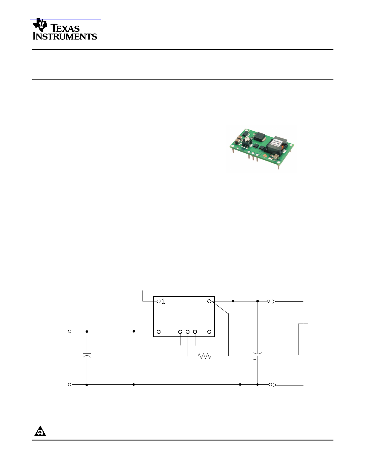
*See the for capacitor recommendation.Application Information
#R
SET
is required to adjust the output voltage lower than -3 V. See the for values.Application Information
STANDARD APPLICATION
4 5
R
SET
#
1 %, 0.05 W
(Required)
L
O
A
D
查询PTN78020A供应商
25-W, WIDE-INPUT ADJUSTABLE POSITIVE-TO-NEGATIVE VOLTAGE
FEATURES APPLICATIONS
• 4-A Output Current
• Wide-Input Voltage
(9 V to 29 V)
• Wide-Output Voltage Adjust
(–15 V to –3 V)
• High Efficiency (Up to 87%)
• Output Current Limit
• Overtemperature Shutdown
• Undervoltage Lockout
• Operating Temperature: –40°C to 85°C
• Surface-Mount Package Available
PTN78020A
SLTS244A – APRIL 2005 – REVISED MAY 2005
REGULATOR MODULE
• General-Purpose, Industrial Controls,
HVAC Systems, Test and Measurement,
Medical Instrumentation, AC/DC Adaptors,
Vehicles, Marine, and Avionics
DESCRIPTION
The PTN78020A is a series of high-efficiency buck-boost-integrated switching regulators (ISR), that represent the
third generation in the evolution of high-performance power modules designed for industrial use. The wide-input
voltage range makes these modules suitable for a variety of applications that operate off 12–V, 24–V, and
tightly-regulated 28–V dc power. In new designs, they should be considered in place of the PT6640 and
PT78NR100 series of single in-line pin (SIP) products. The PTN78020A is smaller and lighter than its
predecessors, and has either similar or improved electrical performance characteristics. The caseless,
double-sided package has excellent thermal characteristics, and is compatible with TI's roadmap for RoHS and
lead-free compliance.
The PTN78020A operates over an input voltage range of 9 V to 29 V, and provides high-efficiency,
positive-to-negative voltage conversion for loads of up to 4 A. The output voltage is set using a single external
resistor, and may be adjusted to any value within the range, –15 V to –3 V.
PRODUCTION DATA information is current as of publication date.
Products conform to specifications per the terms of the Texas
Instruments standard warranty. Production processing does not
necessarily include testing of all parameters.
Please be aware that an important notice concerning availability, standard warranty, and use in critical applications of Texas
Instruments semiconductor products and disclaimers thereto appears at the end of this data sheet.
Copyright © 2005, Texas Instruments Incorporated
www.ti.com
PTN78020A
SLTS244A – APRIL 2005 – REVISED MAY 2005
These devices have limited built-in ESD protection. The leads should be shorted together or the device
placed in conductive foam during storage or handling to prevent electrostatic damage to the MOS gates.
ORDERING INFORMATION
PTN78020 (Basic Model)
Output Voltage Part Number Description Package Designator
PTN78020AAH Horizontal T/H (Pb-free) EUK-7
–15 V to –3 V PTN78020AAS
PTN78020AAZ
(1) Add a T suffix for tape and reel option on SMD packages.
(2) Standard option specifies Sn/Pb solder ball material.
(3) Lead (Pb) - free option specifies Sn/Ag solder ball material.
(1) (2)
(1) (3)
Horizontal SMD (standard) EUL-7
Horizontal SMD (Pb-free) EUL-7
ABSOLUTE MAXIMUM RATINGS
(1)
over operating free-air temperature range unless otherwise noted
all voltages with respect to GND
T
A
T
S
P
O
(1) Stresses beyond those listed under absolute maximum ratings may cause permanent damage to the device. These are stress ratings
Operating free-air temperature Over VIrange –40°C to 85°C
Solder reflow temperature
Surface temperature of module body or
pins
Horizontal SMD (suffix AS) 235°C
Horizontal SMD (suffix AZ) 260 ° C
Storage temperature –40°C to 125°C
Output power |V
| ≥ 12 V 25 W
O
only, and functional operation of the device at these or any other conditions beyond those indicated under recommended operating
conditions is not implied. Exposure to absolute-maximum-rated conditions for extended periods may affect device reliability.
RECOMMENDED OPERATING CONDITIONS
MIN MAX UNIT
V
I
T
A
Input voltage 9 32 – |VO| V
Operating free-air temperature -40 85 °C
PACKAGE SPECIFICATIONS
PTN78020x (Suffix AH, AS, & AZ)
Weight 7.3 grams
Flammability Meets UL 94 V-O
Mechanical shock
Per Mil-STD-883D, Method 2002.3, 1 ms, ½ sine,
mounted
Mechanical vibration Mil-STD-883D, Method 2007.2, 20-2000 Hz
(1) Qualification limit.
Horizontal T/H (suffix AH) 250 Gs
Horizontal SMD (suffix AS and AZ) 125 Gs
Horizontal T/H (suffix AH) 20 Gs
Horizontal SMD (suffix AS and AZ) 10 Gs
UNIT
(1)
(1)
(1)
(1)
2
www.ti.com
PTN78020A
SLTS244A – APRIL 2005 – REVISED MAY 2005
ELECTRICAL CHARACTERISTICS
operating at 25°C free-air temperature, VI= 20 V, VO= –5 V, IO= IO(max), CI= 100 µF and 4x 4.7 µF, C
otherwise noted)
PARAMETER TEST CONDITIONS MIN TYP MAX UNIT
VO= -3 V 0.1 4
I
O
V
I
Output current A
Input voltage range Over IOrange V
TA= 25 ° C, natural convection airflow
Set-point voltage tolerance TA= 25°C ±2%
Temperature variation -40°C to +85°C -0.5%
V
O
Line regulation Over VIrange -10 mV
Load regulation Over IOrange -10 mV
Total output voltage variation -3%
Includes set point, line, load
-40 < TA< 85°C
VO(adj) Output voltage adjust range 9 V ≤ VI≤ (32 – |VO|) V -15 - 3 V
η Efficiency
VI= 12 V, R
VI= 12 V, R
VI= 20 V, R
VI= 24 V, R
= 100 Ω, VO= –15 V 87%
SET
= 2 k Ω, VO= –12 V 86%
SET
= 28.7 k Ω, VO= –5 V 82%
SET
= 221 k Ω, VO= –3.3 V 77%
SET
Output voltage ripple 20-MHz bandwidth 1% V
I
O (LIM)
Current limit threshold ∆ VO= –50 mV 8.5 A
1 A/µs load step from 50% to 100%
IOmax
Transient response
VOover/undershoot 5 %V
F
S
Switching frequency Over VIand IOranges 440 550 660 kHz
UVLO Undervoltage lockout VIincreasing 5.5 V
C
I
External input capacitance µF
Ceramic 18.8
Nonceramic 100
Ceramic 200
C
O
External output capacitance Nonceramic 100
Equivalent series resistance (nonceramic) 10
MTBF Calculated reliability 5.6
Per Telcordia SR-332, 50% stress,
TA= 40°C, ground benign
VO= -5 V 0.1 4
VO= -12 V 0.1 2.1
VO= -15 V 0.1 1.67
VO= -3 V 9 29
VO= -5 V 9 27
VO= -12 V 9 20
VO= -15 V 9 17
Recovery time 200 µs
(4)
(4)
(5)
(6)
= 100 µF (unless
O
(1)
(1)
(1)
(1)
(2)
(2)
(2)
(2)
(3)
(3)
O
2,000
V
(PP)
O
µF
m Ω
6
10
Hrs
(1) The maximum output current is 4 A, or a maximum output power of 25 W, whichever is less.
(2) The maximum input voltage is limited and defined to be (32 – |VO|) volts.
(3) The set-point voltage tolerance is affected by the tolerance and stability of R
tolerance of 1% with 100 ppm/°C or better temperature stability.
(4) A minimum 100-µF electrolytic and four 4.7-µF ceramic capacitors are required across the input (V
Locate the ceramic capacitors close to the module.
. The stated limit is unconditionally met if R
SET
and GND) for proper operation.
I
SET
(5) 100 µF of output capacitance is required for proper operation. See the application information for further guidance.
(6) This is the typical ESR for all the electrolytic (nonceramic) capacitance. Use 17 m Ω as the minimum when using max-ESR values to
calculate.
has a
3
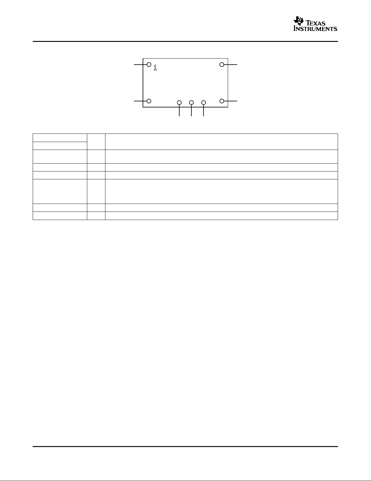
www.ti.com
PTN78020A
(Top View)
1
2
7
6
543
PTN78020A
SLTS244A – APRIL 2005 – REVISED MAY 2005
PIN ASSIGNMENT
TERMINAL FUNCTIONS
TERMINAL
NAME NO.
V
O
V
I
N/C 3 This pin is active and must be isolated from any electrical connection.
VOAdjust 4 I
N/C 5 This pin is active and must be isolated from any electrical connection.
GND 6 I/O The common ground connection for VIand VOpower connections.
1, 7 O
2 I The positive input voltage power node to the module, which is referenced to common GND.
I/O DESCRIPTION
The negative output voltage power connection. It is also the reference for the VOAdjust control input. For
proper operation, pins 1 and 7 must be connected.
A 1% resistor must be connected between pin 4 and pin 7 to set the output voltage of the module lower
than -3 V. If left open-circuit, the output voltage defaults to -3 V. The temperature stability of the resistor
should be 100 ppm/°C (or better). The set-point range is -15 V to -3 V. The standard resistor value for a
number of common output voltages is provided in the application information.
4
www.ti.com
0
1 2
3
4
50
40
55
45
65
60
70
75
80
85
95
90
100
V = -5 V
O
V = -3 V
O
V = -12 V
O
V = -15 V
O
Efficiency - %
I - Output Current - A
O
0
1 2
3
4
I - Output Current - A
O
0
50
100
150
250
200
300
V = -5 V
O
V = -3 V
O
V = -12 V
O
V = -15 V
O
V - Output Voltage Ripple - mV
O PP
0 1 2 3 4
I - Output Current - A
O
0
1
0.5
1.5
2
3
2.5
3.5
4
4.5
5
V = -5 V
O
V = -3 V
O
V = -12 V
O
V = -15 V
O
P - Power Dissipation - W
D
0 0.4 0.8 1.2 1.6
I - Output Current - A
O
20
30
50
40
60
70
80
90
V = -15 V
O
200 LFM
100 LFM
Nat conv
Ambient Temperature - C
o
0 0.3 0.6 0.9 1.51.2 1.8 2.1
I - Output Current - A
O
20
30
50
40
60
70
80
90
Ambient Temperature - C
o
200 LFM
100 LFM
Nat conv
V = -12 V
O
0
1 2
3
4
I - Output Current - A
O
20
30
50
40
60
70
80
90
V = -5 V
O
200 LFM
100 LFM
Nat conv
Ambient Temperature - C
o
SLTS244A – APRIL 2005 – REVISED MAY 2005
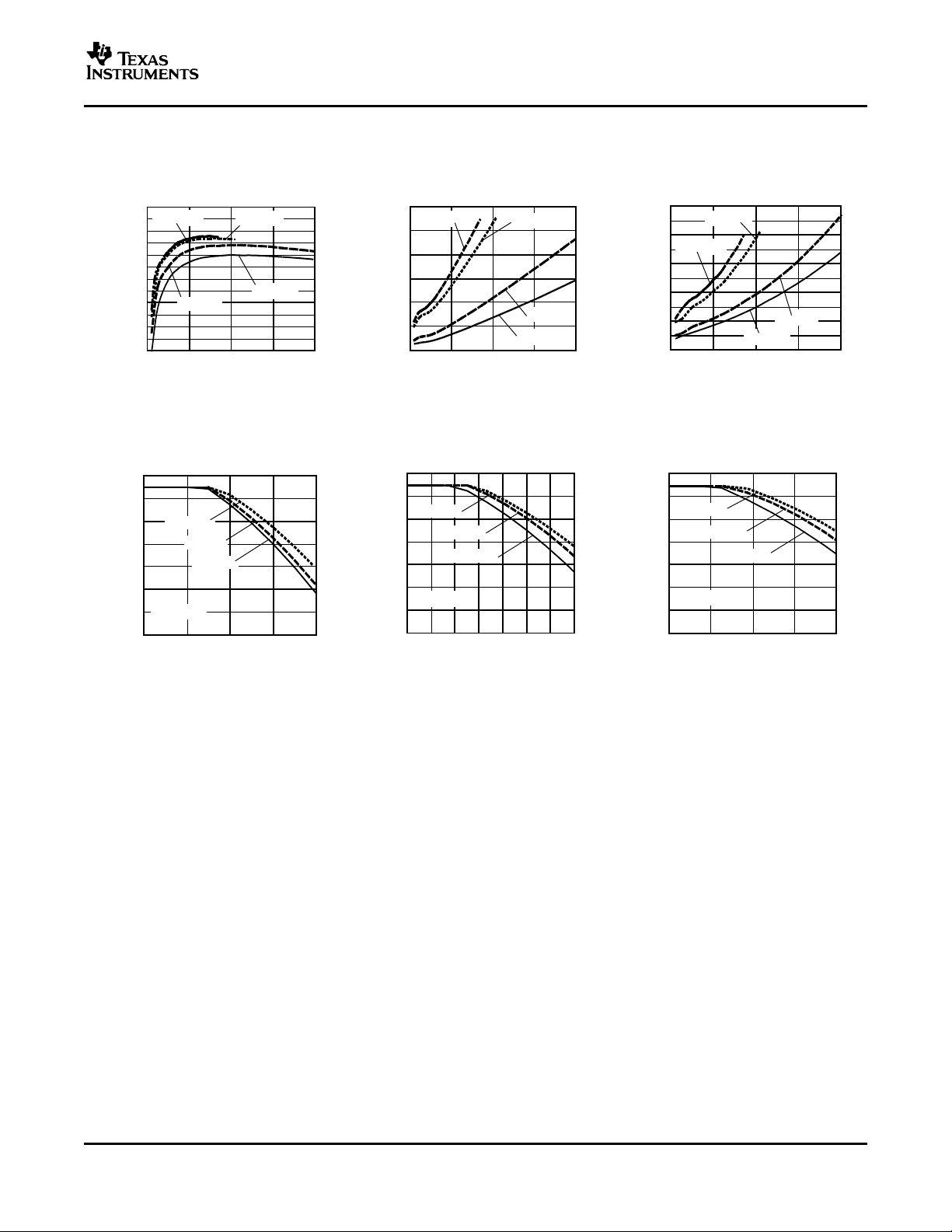
TYPICAL CHARACTERISTICS (9-V INPUT)
(1) (2)
EFFICIENCY OUTPUT VOLTAGE RIPPLE POWER DISSIPATION
vs vs vs
OUTPUT CURRENT OUTPUT CURRENT OUTPUT CURRENT
Figure 1. Figure 2. Figure 3.
PTN78020A
TEMPERATURE DERATING TEMPERATURE DERATING TEMPERATURE DERATING
vs vs vs
OUTPUT CURRENT OUTPUT CURRENT OUTPUT CURRENT
Figure 4. Figure 5. Figure 6.
(1) The electrical characteristic data has been developed from actual products tested at 25 ° C. This data is considered typical for the
converter. Applies to Figure 1 , Figure 2 , and Figure 3 .
(2) The temperature derating curves represent the conditions at which internal components are at or below the manufacturer's maximum
operating temperatures. Derating limits apply to modules soldered directly to a 100 mm x 100 mm, double-sided PCB with 2 oz. copper.
Applies to Figure 4 , Figure 5 , and Figure 6 .
5
www.ti.com
0 1 2 3 4
50
40
55
45
65
60
70
75
80
85
95
90
100
V = -5 V
O
V = -3 V
O
V = -12 V
O
V = -15 V
O
Efficiency - %
I - Output Current - A
O
0
1 2
3
4
I - Output Current - A
O
0
50
100
150
250
200
300
V = -5 V
O
V = -3 V
O
V = -12 V
O
V = -15 V
O
V - Output Voltage Ripple - mV
O PP
0 1 2 3 4
I - Output Current - A
O
0
1
0.5
1.5
2
3
2.5
3.5
4
4.5
5
V = -5 V
O
V = -3 V
O
V = -12 V
O
V = -15 V
O
P - Power Dissipation - W
D
0 0.3 0.6 0.9 1.51.2 1.8 2.1
I - Output Current - A
O
20
30
50
40
60
70
80
90
V = -12 V
O
200 LFM
100 LFM
Nat conv
Ambient Temperature - C
o
0 0.4 0.8 1.2 1.6
I - Output Current - A
O
20
30
50
40
60
70
80
90
V = -15 V
O
200 LFM
100 LFM
Nat conv
Ambient Temperature - C
o
0 1 2 3 4
I - Output Current - A
O
20
30
50
40
60
70
80
90
V = -5 V
O
200 LFM
100 LFM
Nat conv
Ambient Temperature - C
o
PTN78020A
SLTS244A – APRIL 2005 – REVISED MAY 2005
EFFICIENCY OUTPUT VOLTAGE RIPPLE POWER DISSIPATION
vs vs vs
OUTPUT CURRENT OUTPUT CURRENT OUTPUT CURRENT
Figure 7. Figure 8. Figure 9.
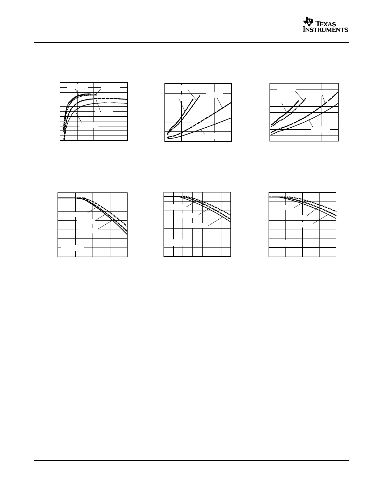
TYPICAL CHARACTERISTICS (12-V INPUT)
(1) (2)
TEMPERATURE DERATING TEMPERATURE DERATING TEMPERATURE DERATING
vs vs vs
OUTPUT CURRENT OUTPUT CURRENT OUTPUT CURRENT
Figure 10. Figure 11. Figure 12.
(1) The electrical characteristic data has been developed from actual products tested at 25 ° C. This data is considered typical for the
converter. Applies to Figure 7 , Figure 8 , and Figure 9 .
(2) The temperature derating curves represent the conditions at which internal components are at or below the manufacturer's maximum
operating temperatures. Derating limits apply to modules soldered directly to a 100 mm x 100 mm, double-sided PCB with 2 oz. copper.
Applies to Figure 10 , Figure 11 , and Figure 12 .
6

www.ti.com
TYPICAL CHARACTERISTICS (24-V INPUT)
0 1 2 3 4
50
40
60
70
80
90
V = -5 V
O
V = -3 V
O
Efficiency - %
I - Output Current - A
O
0
1 2
3
4
I - Output Current - A
O
0
20
40
60
100
80
120
140
V = -5 V
O
V = -3 V
O
V - Output Voltage Ripple - mV
O PP
0 1 2 3 4
I - Output Current - A
O
0
1
0.5
1.5
2
3
2.5
3.5
4
4.5
5
V = -5 V
O
V = -3 V
O
P - Power Dissipation - W
D
0 1 2 3 4
I - Output Current - A
O
20
30
50
40
60
70
80
90
V = -5 V
O
200 LFM
100 LFM
Nat conv
Ambient Temperature - C
o
EFFICIENCY OUTPUT VOLTAGE RIPPLE
vs vs
OUTPUT CURRENT OUTPUT CURRENT
Figure 13. Figure 14.
PTN78020A
SLTS244A – APRIL 2005 – REVISED MAY 2005
(1) (2)
POWER DISSIPATION TEMPERATURE DERATING
vs vs
OUTPUT CURRENT OUTPUT CURRENT
Figure 15. Figure 16.
(1) The electrical characteristic data has been developed from actual products tested at 25 ° C. This data is considered typical for the
converter. Applies to Figure 13 , Figure 14 , and Figure 15 .
(2) The temperature derating curves represent the conditions at which internal components are at or below the manufacturer's maximum
operating temperatures. Derating limits apply to modules soldered directly to a 100 mm x 100 mm, double-sided PCB with 2 oz. copper.
Applies to Figure 16 .
7

www.ti.com
R = 54.9 k
SET
W ´
1.25 V
| |V - 3 V
O
- 5.62 kW
GND GND
PTN78020A
6
1, 72
Adj
GND
V
O
V
I
V
I
V
O
4
+
C2C1
R
SET
0.05 W
1%
C3
+
PTN78020A
SLTS244A – APRIL 2005 – REVISED MAY 2005
APPLICATION INFORMATION
Adjusting the Output Voltage of the PTN78020A Wide-Output Adjust Power Modules
General
A resistor must be connected directly between the V
the output voltage lower than –3 V. The adjustment range is from –15 V to –3 V. If pin 4 is left open, the output
voltage defaults to the highest value, –3 V.
Table 1 gives the standard resistor value for a number of common voltages, and with the actual output voltage
that the value produces. For other output voltages, the resistor value can either be calculated using the following
formula, or simply selected from the range of values given in Table 2 . Figure 17 shows the placement of the
required resistor.
Input Voltage Considerations
The PTN78020A is a buck-boost switching regulator. In order that the output remains in regulation, the input
voltage must not exceed the output by a maximum differential voltage.
Another consideration is the pulse width modulation (PWM) range of the regulator's internal control circuit. For
stable operation, its operating duty cycle should not be lower than some minimum percentage. This defines the
maximum advisable ratio between the regulator's input and output voltage magnitudes.
For satisfactory performance, the maximum operating input voltage range must be equal to (32 - |V
Adjust control (pin 4) and the output voltage (pin 7) to set
O
|) volts.
O
As an example, Table 1 gives the operating input voltage range for the common output bus voltages. In addition,
the Electrical Characteristics define the available output voltage adjust range for various input voltages.
Table 1. Standard Values of R
V
O
(Required) (Standard Value) (Actual) VIRange
–15 V 100 Ω –14.997 V 9 V to 17 V
–12 V 2 k Ω –12.006 V 9 V to 20 V
–5 V 28.7 k Ω –5.000 V 9 V to 27 V
–3.3 V 221 k Ω –3.303 V 9 V to 28.7 V
(1) A 0.05-W rated resistor may be used. The tolerance should be 1%, with a temperature stability of 100 ppm/°C (or
better). Place the resistor as close to the regulator as possible. Connect the resistor directly between pins 4 and 1
using dedicated PCB traces.
(2) Never connect capacitors from VOAdjust to either GND or V
the stability of the regulator.
Figure 17. V
8
R
SET
O
Voltages
Adjust Resistor Placement
for Common Output
set
V
O
. Any capacitance added to the VOAdjust pin affects
out
Operating

www.ti.com
SLTS244A – APRIL 2005 – REVISED MAY 2005
Table 2. Output Voltage Set-Point Resistor Values
VORequired R
–15.0 V 99 Ω –11.9 V 2.09 k Ω –8.8 V 6.21 k Ω
–14.9 V 147 Ω –11.8 V 2.18 k Ω –8.6 V 6.63 k Ω
–14.8 V 196 Ω –11.7 V 2.27 k Ω –8.4 V 7.09 k Ω
–14.7 V 245 Ω –11.6 V 2.36 k Ω –8.2 V 7.58 k Ω
–14.6 V 296 Ω –11.5 V 2.45 k Ω –8.0 V 8.11 k Ω
–14.5 V 347 Ω –11.4 V 2.55 k Ω –7.8 V 8.68 k Ω
–14.4 V 400 Ω –11.3 V 2.65 k Ω –7.6 V 9.30 k Ω
–14.3 V 453 Ω –11.2 V 2.75 k Ω –7.4 V 9.98 k Ω
–14.2 V 507 Ω –11.1 V 2.82 k Ω –7.2 V 10.7 k Ω
–14.1 V 562 Ω –11.0 V 2.96 k Ω –7.0 V 11.5 k Ω
–14.0 V 619 Ω –10.9 V 3.07 k Ω –6.8 V 12.4 k Ω
–13.9 V 676 Ω –10.8 V 3.18 k Ω –6.6 V 13.4 k Ω
–13.8 V 734 Ω –10.7 V 3.29 k Ω –6.4 V 14.6 k Ω
–13.7 V 794 Ω –10.6 V 3.41 k Ω –6.2 V 15.8 k Ω
–13.6 V 854 Ω –10.5 V 3.53 k Ω –6.0 V 17.3 k Ω
–13.5 V 916 Ω –10.4 V 3.65 k Ω –5.8 V 18.9 k Ω
–13.4 V 979 Ω –10.3 V 3.78 k Ω –5.6 V 20.7 k Ω
–13.3 V 1.04 k Ω –10.2 V 3.91 k Ω –5.4 V 22.9 k Ω
–13.2 V 1.11 k Ω –10.1 V 4.04 k Ω –5.2 V 25.6 k Ω
–13.1 V 1.18 k Ω –10.0 V 4.18 k Ω –5.0 V 28.7 k Ω
–13.0 V 1.24 k Ω –9.9 V 4.33 k Ω –4.8 V 32.5 k Ω
–12.9 V 1.31 k Ω –9.8 V 4.47 k Ω –4.6 V 37.2 k Ω
–12.8 V 1.38 k Ω –9.7 V 4.62 k Ω –4.4 V 43.4 k Ω
–12.7 V 1.46 k Ω –9.6 V 4.78 k Ω –4.2 V 51.6 k Ω
–12.6 V 1.52 k Ω –9.5 V 4.94 k Ω –4.0 V 63.0 k Ω
–12.5 V 1.60 k Ω –9.4 V 5.10 k Ω –3.8 V 80.1 k Ω
–12.4 V 1.68 k Ω –9.3 V 5.27 k Ω –3.6 V 109 k Ω
–12.3 V 1.76 k Ω –9.2 V 5.45 k Ω –3.4 V 166 k Ω
–12.2 V 1.84 k Ω –9.1 V 5.63 k Ω –3.2 V 338 k Ω
–12.1 V 1.92 k Ω –9.0 V 5.82 k Ω –3.0 V OPEN
–12.0 V 2.01 k Ω –8.9 V 6.01 k Ω
SET
VORequired R
SET
VORequired R
PTN78020A
SET
9

www.ti.com
PTN78020A
SLTS244A – APRIL 2005 – REVISED MAY 2005
CAPACITOR RECOMMENDATIONS FOR THE PTN78020 WIDE-OUTPUT
ADJUST POWER MODULES
Input Capacitor
The minimum requirement for the input capacitance is 18.8-µF (4× 4.7-µF) ceramic capacitance, in either a X5R
or X7R temperature characteristic, and 100-µF of nonceramic capacitance. Ceramic capacitors should be located
within 0.5 inch (1,27 cm) of the regulator's input pins. Electrolytic capacitors must be used at the input in addition
to the required ceramic capacitance. The minimum ripple current rating for any nonceramic capacitance must be
at least 750 mA rms for output currents of 3 A or less. The ripple current rating of electrolytic capacitors is a
major consideration when they are used at the input. This ripple current requirement can be reduced by placing
more ceramic capacitors at the input, in addition to the minimum required 18.8-µF.
Tantalum capacitors are not recommended for use at the input bus, as none were found to meet the minimum
voltage rating of 2 × (maximum dc voltage + ac ripple). This voltage derating is standard practice for regular
tantalum capacitors to ensure reliability. Polymer-tantalum capacitors are more reliable, and are available with a
maximum rating of typically 20 V. These can be used with input voltages up to 16 V.
Output Capacitor
The minimum electrolytic capacitance required to ensure stability is a 100-µF capacitor. Either ceramic or
electrolytic-type capacitors can be used. The minimum ripple current rating for the nonceramic capacitance must
be at least 250 mA rms. The stability of the module and voltage tolerances is compromised if the capacitor is not
placed near the output bus pins. A high-quality, computer-grade electrolytic capacitor should be adequate. A
ceramic capacitor can be also be located within 0.5 inch (1,27 cm) of the output pin.
For applications with load transients (sudden changes in load current), the regulator response improves with
additional capacitance. Additional electrolytic capacitors should be located close to the load circuit. These
capacitors provide decoupling over the frequency range, 2 kHz to 150 kHz. Aluminum electrolytic capacitors are
suitable for ambient temperatures above 0°C. For operation below 0°C, tantalum or Os-Con-type capacitors are
recommended. When using one or more nonceramic capacitors, the calculated equivalent ESR should be no
lower than 10 mΩ (17 m Ω using the manufacturer's maximum ESR for a single capacitor). A list of recommended
capacitors and vendors are identified in Table 3 .
Ceramic Capacitors
Above 150 kHz, the performance of aluminum electrolytic capacitors becomes less effective. To further reduce
the reflected input ripple current or the output transient response, multilayer ceramic capacitors must be added.
Ceramic capacitors have low ESR, and their resonant frequency is higher than the bandwidth of the regulator.
When placed at the output, their combined ESR is not critical as long as the total value of ceramic capacitance
does not exceed 200 µF.
Tantalum Capacitors
Tantalum-type capacitors may be used at the output, and are recommended for applications where the ambient
operating temperature can be less than 0°C. The AVX TPS, Sprague 593D/594/595, and Kemet
T495/T510/T520 capacitors series are suggested over many other tantalum types due to their rated surge, power
dissipation, and ripple current capability. As a caution, many general-purpose tantalum capacitors have
considerably higher ESR, reduced power dissipation, and lower ripple current capability. These capacitors are
also less reliable as they have lower power dissipation and surge current ratings. Tantalum capacitors that do not
have a stated ESR or surge current rating are not recommended for power applications. When specifying
Os-Con and polymer-tantalum capacitors for the output, the minimum ESR limit is encountered well before the
maximum capacitance value is reached.
Capacitor Table
The capacitor table, Table 3 , identifies the characteristics of capacitors from vendors with acceptable ESR and
ripple current (rms) ratings. The recommended number of capacitors required at both the input and output buses
is identified for each capacitor type. This is not an extensive capacitor list. Capacitors from other vendors are
available with comparable specifications. Those listed are for guidance. The rms rating and ESR (at 100 kHz) are
critical parameters necessary to ensure both optimum regulator performance and long capacitor life.
10

www.ti.com
PTN78020A
SLTS244A – APRIL 2005 – REVISED MAY 2005
Designing for Load Transients
The transient response of the dc/dc converter has been characterized using a load transient with a di/dt of
1 A/µs. The typical voltage deviation for this load transient is given in the data sheet specification table using the
required value of output capacitance. As the di/dt of a transient is increased, the response of a converter's
regulation circuit ultimately depends on its output capacitor decoupling network. This is an inherent limitation of
any dc/dc converter once the speed of the transient exceeds its bandwidth capability. If the target application
specifies a higher di/dt or lower voltage deviation, the requirement can only be met with additional output
capacitor decoupling. In these cases, special attention must be paid to the type, value, and ESR of the
capacitors selected.
Table 3. Recommended Input/Output Capacitors
CAPACITOR CHARACTERISTICS QUANTITY
CAPACITOR VENDOR/
COMPONENT
SERIES
WORKING MAXIMUM PHYSICAL
VOLTAGE RIPPLE SIZE
VALUE SERIES INPUT OUTPUT
(V) CURRENT (mm)
EQUIVALENT
(µF) RESISTANCE BUS BUS
(ESR) ( Ω )
FC( Radial) 35 180 0.090 755 10 × 16 1 1 EEUFC1V331 (VI< 30 V)
FK (SMD) 50 330 0.12 900 12,5 × 13,5 1
United Chemi-Con PXA (SMD) 16 150 0.026 3430 10 × 12,2 ≤ 1 PXA16VC151MJ80TP (VI, |VO|
PS 25 100 0.020 4320 10 × 12,5 1
LXZ 35 220 0.090 760 10 × 12,5 1
MVZ (SMD) 25 470 0.090 670 10 × 10 1 1 MVZ25VC471MJ10TP (VI< 20
Nichicon UWG (SMD) 35 330 0.15 670 10 × 10 1 1 UWG1V331MNR1GS
F550 (Tantalum) 10 100 0.055 2000 7,7 × 4,3 N/R
HD 50 150 0.061 979 10 × 12,5 1 1 UHD1H151MHR
Sanyo Os-Con SVP (SMD) 20 150 0.020 4300 10 × 12,7 1
SP 20 120 0.024 3110 8 × 10,5 1
20 100 0.085 1543 7,3 L × 4,3 N/R
AVX Tantalum TPS (SMD)
20 100 0.200 > 817 3225 N/R
Murata X5R Ceramic 6.3 100 0.002 >1000 3225 N/R
TDK X5R Ceramic 6.3 100 0.002 >1000 3225 N/R
Murata X5R Ceramic 16 47 0.002 >1000 3225 4
Kemet X5R Ceramic 6.3 47 0.002 >1000 3225 N/R
TDK X5R Ceramic 6.3 47 0.002 >1000 3225 N/R
Murata X5R Ceramic 6.3 47 0.002 >1000 3225 N/R
TDK X7R Ceramic 25 2.2 0.002 >1000 3225 ≥ 8
Murata X7R Ceramic 25 2.2 0.002 >1000 3225 ≥ 8
Kemet X7R Ceramic 25 2.2 0.002 >1000 3225 ≥ 8
AVX X7R Ceramic 25 2.2 0.002 >1000 3225 ≥ 8
85°C
VENDOR
NUMBER
(mArms)
(1)
1 EEVFK1H181Q
(1)
1
(1)
(1)
< 14 V)
≤ 1 25PS100M J12 (VI< 20 V)
1 LXZ35VB221M10X12LL
V)
(2)
(1)
(1)
(2)
W × 4,1 H (|V
(2)
(2)
(2)
(1)
(2)
(2)
(2)
(4)
(4)
(4)
(3)
≤ 3
F551A107MN (VO≤ 5 V)
≤ 1 20SVP150M (VI≤ 16 V)
≤ 1 20SP180M (VI≤ 16 V)
≤ 3 TPSV107M020R0085
| ≤ 10 V)
O
≤ 3 TPSE107M020R0200
(|V
| ≤ 10 V)
O
≤ 2 GRM32ER60J107M
(|V
| ≤ 5.5 V)
O
≤ 2 C3225X5R0J107MT
(|V
| ≤ 5.5 V)
O
≤ 4 GRM32ER61C476M
(|V
| ~ VI≤ 13.5 V)
o
≤ 4 C1210C476K9PAC
(|V
| ≤ 5.5 V)
O
≤ 4 C3225X5R0J476MT
(|V
| ≤ 5.5 V)
O
≤ 4 GRM42-2X5R476M6.3
(|V
| ≤ 5.5 V)
O
1 C3225X7R1E225KT/MT
(|V
| ≤ 20 V)
O
1 GRM32RR71E225K
(|V
| ≤ 20 V)
O
1 C1210C225K3RAC
(VI, |VO| ≤ 20 V)
(4)
1 C12103C225KAT2A
(VI, |VO| ≤ 20 V)
(1) The voltage rating of the input capacitor must be selected for the desired operating input voltage range of the regulator. To operate the
regulator at a higher input voltage, select a capacitor with the next higher voltage rating.
(2) Not recommended (N/R). The voltage rating does not meet the minimum operating limits in most applications.
(3) The maximum voltage rating of the capacitor must be selected for the desired set-point voltage (V
voltage, select a capacitor with a higher voltage rating.
). To operate at a higher output
O
(4) The maximum rating of the ceramic capacitor limits the regulator operating input voltage to 20 V. Select a alternative ceramic
component to operate at a higher input voltage.
11
www.ti.com
PTN78020A
SLTS244A – APRIL 2005 – REVISED MAY 2005
Table 3. Recommended Input/Output Capacitors (continued)
CAPACITOR CHARACTERISTICS QUANTITY
CAPACITOR VENDOR/
COMPONENT
SERIES
Kemet X7R Ceramic 50 1.0 0.002 >1000 3225 N/R
Murata X7R Ceramic 50 4.7 0.002 >1000 3225 ≥ 4 1 GRM32ER71H475KA88L
TDK X7R Ceramic 50 2.2 0.002 >1000 3225 ≥ 8 1 C3225X7R1H225KT
Murata X7R Ceramic 50 1.0 0.002 >1000 3225 N/R
TDK X7R Ceramic 50 1.0 0.002 >1000 3225 N/R
Kemet Radial Through-hole 50 1.0 0.002 >1000 5,08 × 7,62 N/R
Murata Radial Through-hole 50 2.2 0.004 >1000 10 H × 10 ≥ 8 1 RPER71H2R2KK6F03
WORKING MAXIMUM PHYSICAL
VOLTAGE RIPPLE SIZE
(V) CURRENT (mm)
VALUE SERIES INPUT OUTPUT
EQUIVALENT
(µF) RESISTANCE BUS BUS
(ESR) ( Ω )
85°C
(mArms)
× 9,14 H
W × 4 D
VENDOR
NUMBER
(2)
1 C1210C105K5RAC
(2)
1 GRM32RR71H105KA01L
(2)
1 C3225X7R1H105KT
(2)
1 C330C105K5R5CA
12
www.ti.com
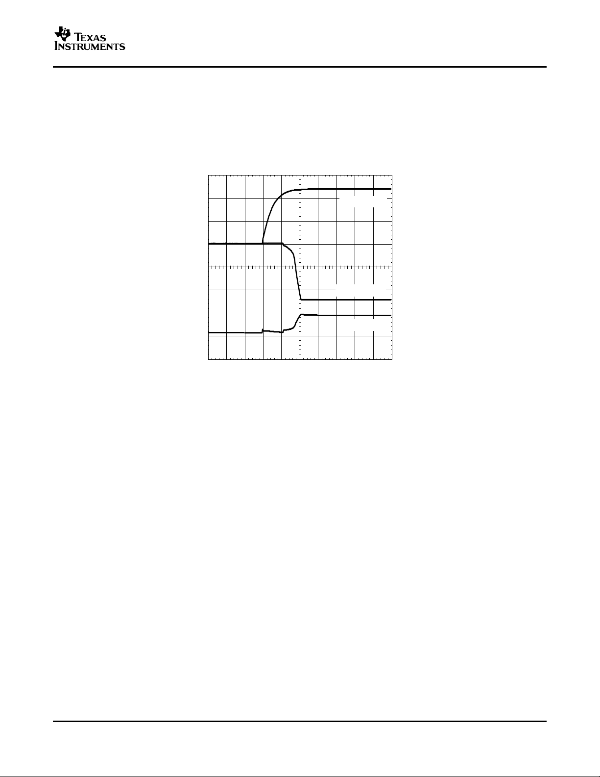
t - Time = 5 ms/div
VI(5 V/div)
VO(2 V/div)
II(2 A/div)
PTN78020A
SLTS244A – APRIL 2005 – REVISED MAY 2005
Power-Up Characteristics
When configured per the standard application, the PTN78020A power module produces a regulated output
voltage following the application of a valid input source voltage. During power up, internal soft-start circuitry slows
the rate that the output voltage rises, thereby limiting the amount of in-rush current that can be drawn from the
input source. The soft-start circuitry introduces a short time delay (typically 5 ms – 10 ms) into the power-up
characteristic. This is from the point that a valid input source is recognized. Figure 18 shows the power-up
waveforms for a PTN78020A, operating from a 12-V input and with the output voltage adjusted to –5-V. The
waveforms were measured with a 3-A resistive load.
Figure 18. Power-Up Waveforms
Undervoltage Lockout
The undervoltage lockout (UVLO) circuit prevents the module from attempting to power up until the input voltage
is above the UVLO threshold. This prevents the module from drawing excessive current from the input source at
power up. Below the UVLO threshold, the module is held off.
Current Limit Protection
The PTN78020 modules protect against load faults with a continuous current limit characteristic. Under a load
fault condition, the output current cannot exceed the current limit value. Attempting to draw current that exceeds
the current limit value causes the module to progressively reduce its output voltage. Current is continuously
supplied to the fault until it is removed. On removal of the fault, the output voltage promptly recovers. When
limiting output current, the regulator experiences higher power dissipation, which increases its temperature. If the
temperature increase is excessive, the module overtemperature protection begins to periodically turn the output
voltage completely off.
Overtemperature Protection
A thermal shutdown mechanism protects the module's internal circuitry against excessively high temperatures. A
rise in temperature may be the result of a drop in airflow, a high ambient temperature, or a sustained current limit
condition. If the junction temperature of the internal control IC rises excessively the module turns itself off,
reducing the output voltage to zero. The module instantly restarts when the sensed temperature decreases by a
few degrees.
Overtemperature protection is a last-resort mechanism to prevent damage to the module. It should not be relied
on as permanent protection against thermal stress. Always operate the module within its temperature derated
limits, for the worst-case operating conditions of output current, ambient temperature, and airflow. Operating the
module above these limits, albeit below the thermal shutdown temperature, reduces the long-term reliability of
the module.
13

www.ti.com
C4
100 F
(Required)
#
m
C3*
4 x 4.7 F
Ceramic
(Required)
m
C2
100 F
Electrolytic
m
C1
1 F
50 V
m
R
SET
C5
1 F
Ceramic
m
GND
GND
PTN78020A
4
1, 72
V
I
V
I
V
O
V
O
GND
6
Adjust
* See the specifications for required value and type.
# See the for suggested value and type.Application Information
PTN78020A
SLTS244A – APRIL 2005 – REVISED MAY 2005
Optional Input/Output Filters
Power modules include internal input and output ceramic capacitors in all of their designs. However, some
applications require much lower levels of either input reflected or output ripple/noise. This application describes
various filters and design techniques found to be successful in reducing both input and output ripple/noise.
Input/Output Capacitors
The easiest way to reduce output ripple and noise is to add one or more 1-µF ceramic capacitors, such as C5
shown in Figure 19 . Ceramic capacitors should be placed close to the output power terminals. A single 1-µF
capacitor reduces the output ripple/noise by 10% to 30% for modules with a rated output current of less than 3 A.
(Note: C4 is required to improve the regulator transient response, and does not reduce output ripple and noise.)
Switching regulators draw current from the input line in pulses at their operating frequency. The amount of
reflected (input) ripple/noise generated is directly proportional to the equivalent source impedance of the power
source including the impedance of any input lines. The addition of C1, minimum 1-µF ceramic capacitor, near the
input power pins, reduces reflected conducted ripple/noise by 10% to 30%.
Figure 19. Adding High-Frequency Bypass Capacitors to the Input and Output
π Filters
If a further reduction in ripple/noise level is required for an application, higher order filters must be used. A π (pi)
filter, employing a ferrite bead (Fair-Rite Pt. No. 2673000701 or equivalent) in series with the input or output
terminals of the regulator reduces the ripple/noise by at least 20 db (see Figure 20 and Figure 21 ). In order for
the inductor to be effective in reduction of ripple and noise-ceramic capacitors are required. (See Capacitor
Recommendations for the PTN78020A for additional information on vendors and component suggestions.)
These inductors plus ceramic capacitors form an excellent filter because of the rejection at the switching
frequency (650 kHz - 1 MHz). The placement of this filter is critical. It must be located as close as possible to the
input or output pins to be effective. The ferrite bead is small (12,5 mm × 3 mm), easy to use, low cost, and has
low dc resistance. Fair-Rite also manufactures a surface-mount bead (part number 2773021447), through hole
(part number 2673000701) rated to 5 A. 1-µH to 5-µH inductors can be used in place of the ferrite inductor bead.
14

www.ti.com
GND
GND
C6
†
L1
1 - 5 Hm
L2
1 - 5 Hm
PTN78020A
4
1, 72
GND
6
Adjust
C4
100 F
(Required)
#
m
C3*
18.8 F
Ceramic
(Required)
m
C2
100 F
Electrolytic
(Required)
m
C1
1 F
Ceramic
m
C5
1 F
Ceramic
m
R
SET
V
I
V
I
V
O
V
O
* See the specifications for required value and type.
# See the for suggested value and type.
† Recommended for applications with load transients.
Application Information
10
15
20
25
30
35
40
45
0 0.5 1 1.5 2 2.5 3
1 MHz
600 kHz
Attenuation − dB
Load Current − A
PTN78020A
SLTS244A – APRIL 2005 – REVISED MAY 2005
Figure 20. Adding π Filters (I
Figure 21. π -Filter Attenuation vs. Load Current
≤ 4 A)
O
15

PACKAGE OPTION ADDENDUM
www.ti.com
19-Aug-2005
PACKAGING INFORMATION
Orderable Device Status
PTN78020AAH ACTIVE DIP MOD
(1)
Package
Type
Package
Drawing
Pins Package
Qty
Eco Plan
EUK 7 20 TBD Call TI Level-1-235C-UNLIM
ULE
PTN78020AAS ACTIVE DIP MOD
EUL 7 20 TBD Call TI Level-1-235C-UNLIM
ULE
PTN78020AAST ACTIVE DIP MOD
EUL 7 200 TBD Call TI Level-1-235C-UNLIM
ULE
PTN78020AAZ ACTIVE DIP MOD
EUL 7 20 Pb-Free
ULE
PTN78020AAZT ACTIVE DIP MOD
EUL 7 200 Pb-Free
ULE
(1)
The marketing status values are defined as follows:
ACTIVE: Product device recommended for new designs.
LIFEBUY: TI has announced that the device will be discontinued, and a lifetime-buy period is in effect.
NRND: Not recommended for new designs. Device is in production to support existing customers, but TI does not recommend using this part in
a new design.
PREVIEW: Device has been announced but is not in production. Samples may or may not be available.
OBSOLETE: TI has discontinued the production of the device.
(2)
Eco Plan - The planned eco-friendly classification: Pb-Free (RoHS) or Green (RoHS & no Sb/Br) - please check
http://www.ti.com/productcontent for the latest availability information and additional product content details.
TBD: The Pb-Free/Green conversion plan has not been defined.
Pb-Free (RoHS): TI's terms "Lead-Free" or "Pb-Free" mean semiconductor products that are compatible with the current RoHS requirements
for all 6 substances, including the requirement that lead not exceed 0.1% by weight in homogeneous materials. Where designed to be soldered
at high temperatures, TI Pb-Free products are suitable for use in specified lead-free processes.
Green (RoHS & no Sb/Br): TI defines "Green" to mean Pb-Free (RoHS compatible), and free of Bromine (Br) and Antimony (Sb) based flame
retardants (Br or Sb do not exceed 0.1% by weight in homogeneous material)
(RoHS)
(RoHS)
(2)
Lead/Ball Finish MSL Peak Temp
Call TI Level-3-260C-168 HR
Call TI Level-3-260C-168 HR
(3)
(3)
MSL, Peak Temp. -- The Moisture Sensitivity Level rating according to the JEDEC industry standard classifications, and peak solder
temperature.
Important Information and Disclaimer:The information provided on this page represents TI's knowledge and belief as of the date that it is
provided. TI bases its knowledge and belief on information provided by third parties, and makes no representation or warranty as to the
accuracy of such information. Efforts are underway to better integrate information from third parties. TI has taken and continues to take
reasonable steps to provide representative and accurate information but may not have conducted destructive testing or chemical analysis on
incoming materials and chemicals. TI and TI suppliers consider certain information to be proprietary, and thus CAS numbers and other limited
information may not be available for release.
In no event shall TI's liability arising out of such information exceed the total purchase price of the TI part(s) at issue in this document sold by TI
to Customer on an annual basis.
Addendum-Page 1


IMPORTANT NOTICE
Texas Instruments Incorporated and its subsidiaries (TI) reserve the right to make corrections, modifications,
enhancements, improvements, and other changes to its products and services at any time and to discontinue
any product or service without notice. Customers should obtain the latest relevant information before placing
orders and should verify that such information is current and complete. All products are sold subject to TI’s terms
and conditions of sale supplied at the time of order acknowledgment.
TI warrants performance of its hardware products to the specifications applicable at the time of sale in
accordance with TI’s standard warranty. Testing and other quality control techniques are used to the extent TI
deems necessary to support this warranty . Except where mandated by government requirements, testing of all
parameters of each product is not necessarily performed.
TI assumes no liability for applications assistance or customer product design. Customers are responsible for
their products and applications using TI components. To minimize the risks associated with customer products
and applications, customers should provide adequate design and operating safeguards.
TI does not warrant or represent that any license, either express or implied, is granted under any TI patent right,
copyright, mask work right, or other TI intellectual property right relating to any combination, machine, or process
in which TI products or services are used. Information published by TI regarding third-party products or services
does not constitute a license from TI to use such products or services or a warranty or endorsement thereof.
Use of such information may require a license from a third party under the patents or other intellectual property
of the third party, or a license from TI under the patents or other intellectual property of TI.
Reproduction of information in TI data books or data sheets is permissible only if reproduction is without
alteration and is accompanied by all associated warranties, conditions, limitations, and notices. Reproduction
of this information with alteration is an unfair and deceptive business practice. TI is not responsible or liable for
such altered documentation.
Resale of TI products or services with statements different from or beyond the parameters stated by TI for that
product or service voids all express and any implied warranties for the associated TI product or service and
is an unfair and deceptive business practice. TI is not responsible or liable for any such statements.
Following are URLs where you can obtain information on other Texas Instruments products and application
solutions:
Products Applications
Amplifiers amplifier.ti.com Audio www.ti.com/audio
Data Converters dataconverter.ti.com Automotive www.ti.com/automotive
DSP dsp.ti.com Broadband www.ti.com/broadband
Interface interface.ti.com Digital Control www.ti.com/digitalcontrol
Logic logic.ti.com Military www.ti.com/military
Power Mgmt power.ti.com Optical Networking www.ti.com/opticalnetwork
Microcontrollers microcontroller.ti.com Security www.ti.com/security
Telephony www.ti.com/telephony
Video & Imaging www.ti.com/video
Wireless www.ti.com/wireless
Mailing Address: Texas Instruments
Post Office Box 655303 Dallas, Texas 75265
Copyright 2005, Texas Instruments Incorporated
 Loading...