

Page 1
(25,4 mm x 15,75 mm)
NOMINAL SIZE
1 in. x 0.62 in
查询PTH05060Y供应商
PTH03060Y
PTH05060Y, PTH12060Y
www.ti.com
SLTS222A–MARCH 2004 – REVISED OCTOBER 2005
10-A NON-ISOLATED DDR/QDR
MEMORY BUS TERMINATION MODULES
FEATURES
• VTTBus Termination Output • 57 W/in3Power Density
(Output Tracks the System V
• 10 A Output Current UL/cUL60950, EN60950, VDE
• 3.3-V, 5-V or 12-V Input Voltage • Point-of-Load Alliance (POLA™) Compatible
• DDR and QDR Compatible
• On/Off Inhibit (for VTTStandby)
• Undervoltage Lockout
• Operating Temperature: –40°Cto85°C
• Efficiencies up to 91%
• Output Overcurrent Protection (Non-Latching,
Auto-Reset)
DESCRIPTION
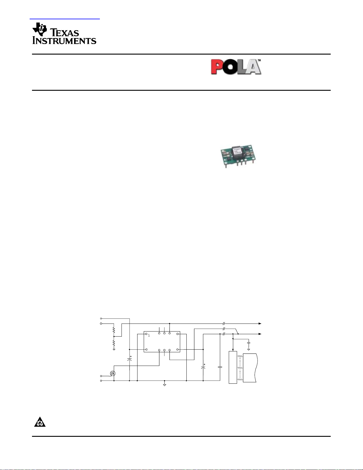
The PTHxx060Y are a series of ready-to-use switching regulator modules from Texas Instruments designed
specifically for bus termination in DDR and QDR memory applications. Operating from either a 3.3-V, 5-V or 12-V
input, the modules generate a VTToutput that will source or sink up to 10 A of current to accurately track their
V
input. VTTis the required bus termination supply voltage, and V
REF
and chipset bus receiver comparators. V
Both the PTHxx060Y series employs an actively switched synchronous rectifier output to provide state-of-the-art
stepdown switching conversion. The products are small in size (1 in × 0.62 in), and are an ideal choice where
space, performance, and high efficiency are desired, along with the convenience of a ready-to-use module.
Operating features include an on/off inhibit and output over-current protection (source mode only). The on/off
inhibit feature allows the VTTbus to be turned off to save power in a standby mode of operation. To ensure tight
load regulation, an output remote sense is also provided. Package options include both throughhole and surface
mount configurations.
REF
)
is usually set to half the V
REF
• Safety Agency Approvals:
is the reference voltage for the memory
REF
power supply voltage.
DDQ
V
IN
V
DDQ
1 k
1 %
1 k
1 %
C
IN
(Required)
Q
1
Standby
GND
CIN = Required Capacitor; 330µF (3.3 ± 5 V Input), 560 µF (12 V Input).
Co
= Required Low-ESR Electrolyitic Capacitor; 470 µF (3.3 ± 5 V Input), 940 µF (12 V Input).
1
= Ceramic Capacitance for Optimum Response to a 3 A (+ 1.5 A) Load Transient; 200 µF (3.3 ± 5 V Input), 400 µF (12 V Input).
Co
2
Co
= Distributed hf-Ceramic Decoupling Capacitors for VTT bus; as Recommended for DDR Memory Applications.
n
BSS138
(Optional)
Please be aware that an important notice concerning availability, standard warranty, and use in critical applications of Texas
Instruments semiconductor products and disclaimers thereto appears at the end of this data sheet.
POLA is a trademark of Texas Instruments.
PRODUCTION DATA information is current as of publication date.
Products conform to specifications per the terms of the Texas
Instruments standard warranty. Production processing does not
necessarily include testing of all parameters.
STANDARD APPLICATION
1
2
10 9 8
PTHxx060Y
(Top View)
3
7
6
54
Co
Low−ESR
(Required)
Co
1
Ceramic
(Optional)
V
REF
V
TT
Co
n
hf−Ceramic
V
TT
Termination Island
2
SSTL−2
Bus
Copyright © 2004–2005, Texas Instruments Incorporated
Page 2
www.ti.com
PTH03060Y
PTH05060Y, PTH12060Y
SLTS222A–MARCH 2004 – REVISED OCTOBER 2005
ORDERING INFORMATION
PTHXX060Y (Base Part Number)
Input Voltage Part Number
PTH03060YAH Horizontal T/H Yes
3.3 V PTH03060YAS Standard SMD No
PTH03060YAZ Optional SMD Yes
PTH05060YAH Horizontal T/H Yes
5 V PTH05060YAS Standard SMD No
PTH05060YAZ Optional SMD Yes
PTH12060YAH Horizontal T/H Yes
12 V PTH12060YAS Standard SMD No
PTH12060YAZ Optional SMD Yes
(1) Add T to end of part number for tape and reel on SMD packages only.
(2) Reference the applicable package reference drawing for the dimensions and PC board layout.
(3) Lead (Pb) –free option specifies Sn/Ag pin solder material.
(4) Standard option specifies 63/37, Sn/Pb pin solder material.
(1)
DESCRIPTION Pb – free and Mechanical Package
RoHS
(4)
(4)
(4)
(2)
(3)
EUW
EUY
(3)
(3)
EUY
EUW
EUY
(3)
(3)
EUY
EUW
EUY
(3)
EUY
ENVIRONMENTAL AND ABSOLUTE MAXIMUM RATINGS
voltages are with respect to GND
UNIT
V
T
T
T
T
(1) For operation below 0°C, the external capacitors must have stable characteristics, use either a low ESR tantalum, Os-Con, or ceramic
(2) During soldering of package version, do not elevate peak temperature of the module, pins or internal components above the stated
Control input voltage –0.3 V to Vin+03 V
REF
Operating temperature Over VINrange –40°Cto85°C
A
range
Wave solder temperature Surface temperature of module body or pins PTHXX060YAH 260°C
wave
Solder reflow temperature Surface temperature of module body or pins
reflow
Storage temperature –40°Cto125°C
s
(5 seconds)
PTHXX060YAS 235°C
PTHXX060YAZ 260°C
Mechanical shock Per Mil-STD-883D, Method 2002.3 1 msec, 1/2 Sine, mounted 500 G
Mechanical vibration Mil-STD-883D, Method 2007.2 20-2000 Hz 20 G
Weight 3.7 grams
Flammability Meets UL 94V-O
capacitor.
maximum.
(1)
(2)
(2)
(2)
2
Page 3
PTH03060Y
PTH05060Y, PTH12060Y
www.ti.com
SLTS222A–MARCH 2004 – REVISED OCTOBER 2005
ELECTRICAL SPECIFICATIONS
TA=25°C; nominal VIN;V
PARAMETER TEST CONDITIONS MIN TYP MAX UNIT
I
O
V
IN
∆V
REF
|V
TT–VREF
η Efficiency I
V
r
trip Overcurrent threshold Reset, followed by auto recovery 20 A
I
o
t
tr
V
tr
UVLO Under-voltage lockout
V
IH
V
IL
I
inhibit Pin to GND 130 µA
IL
inh Input standby current Inhibit control (pin 4) to GND 10 mA
I
IN
f
s
C
IN
CO1, CO2 External output capacitance PTH03060Y/PTH05060Y 200
MTBF Reliability Per Bellcore TR-332 50 % stress, T
Output current Over ∆V
Input voltage range Over IOrange PTH05060Y 4.5 5.5 V
Tracking range for V
| Tracking tolerance to V
VoRipple (pk-pk) 20 MHz bandwidth 20 mVpp
Load transient response
Inhibit control (pin 4) V
Input high voltage
Inhibit control (pin 4) –0.2 0.6
Input low voltage
Inhibit control (pin 4)
Input low curent
Switching frequency Over VINand IOranges kHz
External input capacitance µF
=1.25V;CIN,CO1, and CO2 = typical values; and IO=IOmax (unless otherwise stated)
REF
range Continuous 0 ±10
REF
PTH03060Y 2.95 3.65
PTH12060Y 10.8 13.2
REF
REF
Over line, load and temperature –10 10 mV
0.55 1.8 V
PTH03060Y 86%
= 8 A PTH05060Y 86%
o
PTH12060Y 83%
15 A/µs load step, from:
–1.5 A to 1.5 A
Recovery time 30 µsec
VOover/undershoot 25 40 mV
PTH03060Y 2.45 2.8
Increasing PTH05060Y 4.3 4.45 V
V
IN
PTH12060Y 9.5 10.4
PTH03060Y 2.0 2.40
Dncreasing PTH05060Y 3.4 3.7 V
V
IN
PTH12060Y 8.8 9
–0.5 Open
IN
Referenced to GND
PTH03060Y/PTH05060Y 250 300 350
PTH12060Y 200 250 300
PTH03060Y/PTH05060Y 330
(3)
PTH12060Y 560
Capacitance value: Nonceramic PTH03060Y/PTH05060Y 470
PTH12060Y 940
Capacitance value: Ceramic µF
PTH12060Y 400
Equuivanent series resistance (non-ceramic) 4
=40°C, ground benign 6
A
(4)
(4)
(6)
(1)
(2)
(5)
5500
(5)
5500
(4)
300
(4)
600
A
V
V
µF
mΩ
6
Hrs
10
(1) Rating is conditional on the module being directly soldered to a 4-layer PCB with 1 oz. copper. See the SOA curves or contact the
factory for appropriate derating.
(2) This control pin has an internal pull-up to the input voltage VIN. If it is left open-circuit the module will operate when input power is
applied. A small low-leakage (<100 nA) MOSFET is recommended for control. For further information, consult the related application
note.
(3) An input capacitor is required for proper operation. The capacitor must be rated for a minimum of 300 mA rms (750 mA rms for 12-V
input) of ripple current.
(4) The minimum value of external output capacitance value ensures that VTT meets the specified transient performance requirements for
the memory bus terminations. Lower values of capacitance may be possible when the measured peak change in output current is
consistently less than 3 A.
(5) This is the calculated maximum. The minimum ESR limitation will often result in a lower value. Consult the capacitor application notes
for further guidance.
(6) This is the typcial ESR for all the electrolytic (non-ceramic) output capacitance. Use 7 mΩ as the minimum when using max-ESR values
to calculate.
3
Page 4
www.ti.com
PTH03060Y
PTH05060Y, PTH12060Y
SLTS222A–MARCH 2004 – REVISED OCTOBER 2005
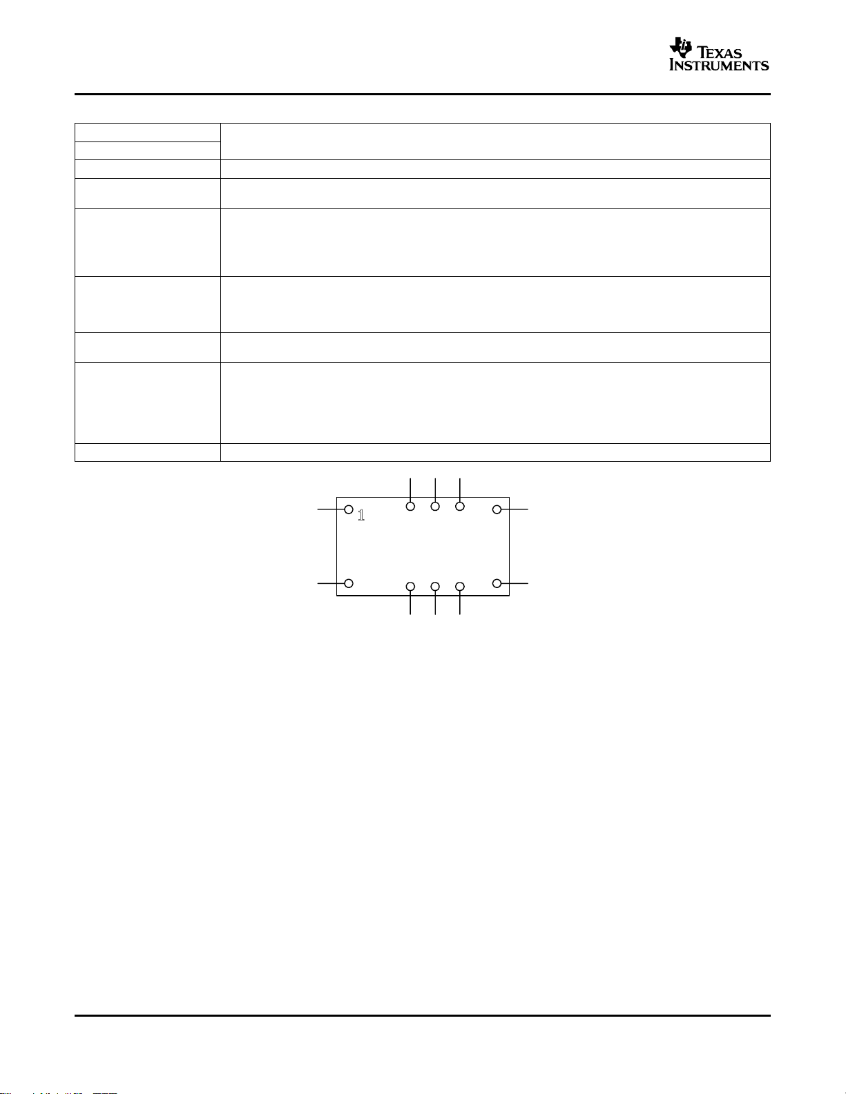
TERMINAL
NAME NO.
V
IN
GND 1, 7
V
REF
V
TT
VoSense 5
Inhibit 3
N/C 4, 9, 10 No connect
DESCRIPTION
2 The positive input voltage power node to the module, which is referenced to common GND.
This is the common ground connection for the VINand VTTpower connections. It is also the 0-VDC reference
for the control inputs.
The module senses the voltage at this input to regulate the output voltage, VTT. The voltage at V
the reference voltage for the system bus receiver comparators. It is normally set to precisely half the bus
8 driver supply voltage (V
V
pin should not exceed 500 Ω. See the Typical DDR Application Diagram in the Application Information
REF
section for reference.
This is the regulated power output from the module with respect to the GND node, and the tracking
termination supply for the application data and address buses. It is precisely regulated to the voltage applied
6
to the module's V
module. Once active it will track the voltage applied at V
The sense input allows the regulation circuit to compensate for voltage drop between the module and the
load. For optimal voltage accuracy VoSense should be connected to VTT.
The Inhibit pin is an open-collector/drain negative logic input that is referenced to GND. Applying a low-level
ground signal to this input turns off the output voltage, VTT. Although the module is inhibited, a voltage, V
will be present at the output terminals, fed through the DDR memory. When the Inhibit is active, the input
current drawn by the regulator is significantly reduced. If the Inhibit pin is left open circuit, the module will
produce an output whenever a valid input source is applied. See the Typical DDR Application Diagram in the
Application Information section for reference.
Terminal Functions
÷ 2), using a resistor divider. The Thevenin impedance of the network driving the
DDQ
input, and is active active about 20 ms after a valid input source is applied to the
REF
REF
.
REF
is also
DDQ
1
7
PTHXX060
(Top View)
10 9 8
2
6
543
4
Page 5
0
1
2
3
4
2468100
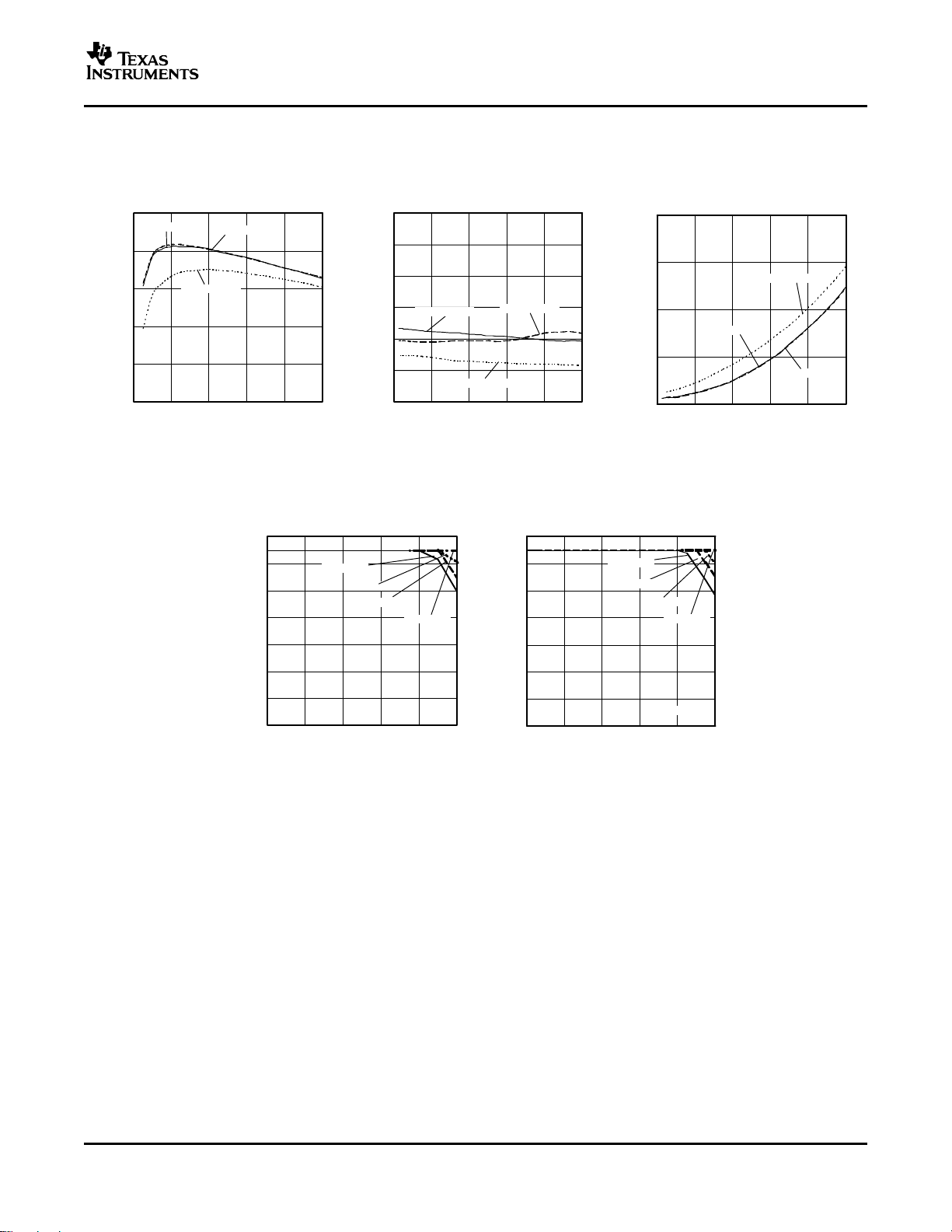
IL − Load Current − A
VIN = 3.3 V
VIN = 12 V
VIN = 5 V
− Power Dissipation − W
P
D
20
30
40
50
60
70
80
90
400 LFM
200 LFM
100 LFM
Nat Cinv
VIN = 12 V
24680
I
L
− Load Current − A
10
T
A
− Ambient Temperature −
5
C
PTH03060Y
PTH05060Y, PTH12060Y
www.ti.com
10 0
90
80
70
Efficiency − %
60
50
SLTS222A–MARCH 2004 – REVISED OCTOBER 2005
TYPICAL CHARACTERISTICS (V
=1.25 V)
REF
(1)(2)
EFFICIENCY OUTPUT RIPPLE POWER DISSIPATION
vs vs vs
LOAD CURRENT LOAD CURRENT LOAD CURRENT
Output Ripple − mV
60
50
40
30
20
10
VIN = 5 V
0
2
− Load Current − A
I
L
VIN = 3.3 V
VIN = 12 V
46 8100
VIN = 5 V
2468100
VIN = 3.3 V
VIN = 12 V
IL − Load Current − A
Figure 1. Figure 2. Figure 3.
PTH03060Y/PTH05060Y AT PTH12060Y ONLY; VIN=12V
NOMINAL V
TEMPERATURE DERATING vs LOAD CURRENT
IN
TEMPERATURE DERATING
vs LOAD CURRENT
90
80
C
5
70
60
50
40
− Ambient Temperature −
A
T
30
20
Nat Cinv
200 LFM
100 LFM
400 LFM
2468100
IL − Load Current − A
Figure 4. Figure 5.
(1) The electrical characteristic data has been developed from actual products tested at 25°C. This data is considered typical for the
converter. Applies to Figure 1, Figure 2, and Figure 3.
(2) The temperature derating curves represent the conditions at which internal components are at or below the manufacturer's maximum
operating temperatures. Derating limits apply to modules soldered directly to a 4 in x 4 in double-sided PCB with 1 oz. copper. For
surface mount packages (AS and AZ suffix), multiple vias (plated through holes) are required to add thermal paths around the power
pins. Please refer to the mechanical specification for more information. Applies to Figure 4, and Figure 5.
5
Page 6
www.ti.com
PTH03060Y
PTH05060Y, PTH12060Y
SLTS222A–MARCH 2004 – REVISED OCTOBER 2005
TYPICAL CHARACTERISTICS
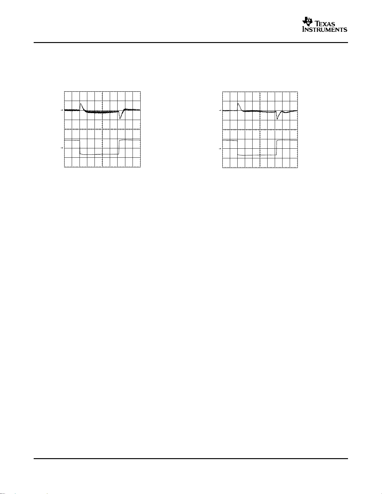
TRANSIENT PERFORMANCE FOR ∆3-A LOAD CHANGE
PTH03060Y/PTH05060Y: SOURCE-SINK-SOURCE PTH12060Y: SOURCE-SINK-SOURCE TRANSIENT
TRANSIENT
50 ms/div
VTT − V
(50 mV/div)
(52A/div)
I
TT
REF
50 ms/div
VTT − V
(50 mV/div)
(2A/div)
I
TT
REF
Figure 6. Figure 7.
6
Page 7

PTH03060Y
PTH05060Y, PTH12060Y
www.ti.com
Typical DDR Application Diagram
Auto-Track
= 5V
V
I
470 µF
+
220 µF
V
I
Inhibit ++
47 µF
V
I
Inhibit +
47 µF
APPLICATION INFORMATION
+SenseMargin ±
PTH05010W
VDDQ I/O Memory
5.51 kΩ
PTH05050Y
DDR Termination
+V
+V
V
ADJ
V
REF
O
2 ×
330 µF
TT
2 ×
330 µF
SLTS222A–MARCH 2004 – REVISED OCTOBER 2005
V
= 1.8 V
DDQ
2 ×
22 µF
2 ×
22 µF
VTT= 0.9 V
1 kΩ
1 kΩ
DDRII/
QDRII
UDG−05096
CAPACITOR RECOMMENDATIONS FOR THE PTH03060Y AND PTH05060Y DDR POWER
MODULES (3.3-V/5-V OPTION)
Input Capacitor
The recommended input capacitor(s) is determined by the 330 µF
minimum ripple current rating.
Ripple current and less than 160 mΩ equivalent series resistance (ESR) values are the major considerations,
along with temperature, when designing with different types of capacitors. Unlike polymer tantalum, regular
tantalum capacitors have a recommended minimum voltage rating of 2 × (maximum DC voltage + AC ripple).
This is standard practice to insure reliability.
For improved ripple reduction on the input bus, ceramic capacitors may be substituted for electrolytic types using
the minimum required capacitance.
Output Capacitors
For applications with load transients (sudden changes in load current), regulator response will benefit from
external output capacitance. The recommended output capacitance of 470 µF will allow the module to meet its
transient response specification (see Electrical Specifications table). For most applications, a high quality
computer-grade aluminum electrolytic capacitor is adequate. These capacitors provide decoupling over the
frequency range, 2 kHz to 150 kHz, and are suitable when ambient temperatures are above 0°C. For operation
below 0°C tantalum, ceramic or Os-Con type capacitors are recommended. When using one or more
non-ceramic capacitors, the calculated equivalent ESR should be no lower than 4 mΩ (7 mΩ using the
manufacturer's maximum ESR for a single capacitor). A list of preferred low-ESR type capacitors are identified in
Table 1.
(1)
minimum capacitance and 300 mArms
7
Page 8

www.ti.com
PTH03060Y
PTH05060Y, PTH12060Y
SLTS222A–MARCH 2004 – REVISED OCTOBER 2005
APPLICATION INFORMATION (continued)
Ceramic Capacitors
Above 150 kHz the performance of aluminum electrolytic capacitors becomes less effective. To further improve
the reflected input ripple current or the output transient response. Multilayer ceramic capacitors have very low
ESR and their resonant frequency higher than the bandwidth of the regulator. They can be used to reduce the
reflected ripple current at the input as well as improve the transient response of the output. When used on the
output their combined ESR is not critical as long as the total value of ceramic capacitance does not exceed
300 µF. Also, to prevent the formation of local resonances, do not place more than five identical ceramic
capacitors in parallel with values of 10 µF or greater.
Tantalum Capacitors
Tantalum type capacitors can be used at both the input and output, and are recommended for applications where
the ambient operating temperature can be less than 0°C. The AVX TPS, Sprague 593D/594/595 and Kemet
T495/T510 capacitor series are suggested over many other tantalum types due to their higher rated surge, power
dissipation, and ripple current capability. As a caution many general purpose tantalum capacitors have
considerably higher ESR, reduced power dissipation and lower ripple current capability. These capacitors are
also less reliable when determining their power dissipation and surge current rating. Tantalum capacitors that do
not have a stated ESR or surge current rating are not recommended for power applications.
When specifying Os-Con and polymer tantalum capacitors for the output, the minimum ESR limit will be
encountered well before the maximum capacitance value is reached.
Capacitor Table
Table 1 identifies the characteristics of capacitors from a number of vendors with acceptable ESR and ripple
current (rms) ratings. The recommended number of capacitors required at both the input and output buses is
identified for each capacitor type.
This is not an extensive capacitor list. Capacitors from other vendors are available with comparable
specifications. Those listed are for guidance. The RMS ripple current rating and ESR (at 100 kHz) are critical
parameters necessary to insure both optimum regulator performance and long capacitor life.
Table 1. Input/Output Capacitors
Capacitor Characteristics Quantity
Capacitor Vendor, Vendor
Type/Series (Style) Part Number
Panasonic, Aluminum
FC (Radial) 10 470 0.117 555 8×11,5 1 1 EEUFC1A471
FK (SMD) 10 470 0.160 600 8×10,2 1 1 EEVFK1A471P
FC (SMD) 10 470 0.150 670 10×10,2 1 1 EEVFC1A471P
United Chemi-Con
PXA, Poly-Aluminum (SMD) 10 470 0.012 5300 10×12,2 1 ≤1 PXA10VC471MJ12TP
PS, Poly-Aluminum (Radial) 10 470 0.012 5300 8×12,2 1 ≤1 10PS470MJ12
LXZ, Aluminum (Radial) 10 470 0.120 555 8×12 1 1 LXZ10VB471M8X12LL
Nichicon Aluminum
WG (SMD) 10 470 0.150 670 10×10 1 1 UWG1A471MNR1GS
HD (Radial) 10 470 0.072 760 8×11.5 1 1 UHD1A471MPR
PM (Radial) 16 330 0.120 625 10×12,5 1 2 UPM1C331MPH6
(1) Capacitor Supplier Verification
Please verify availability of capacitors identified in this table. Capacitor suppliers may recommend alternative part numbers because of
limited availability or obsolete products. In some instances, the capacitor product life cycle may be in decline and have short-term
consideration for obsolescence.
RoHS, Lead-free and Material Details
Please consult capacitor suppliers regarding material composition, RoHS status, lead-free status, and manufacturing process
requirements. Component designators or part number deviations can occur when material composition or soldering requirements are
updated.
Working Max ESR Max Ripple Physical
Voltage at 100 kHz Current at 85°CSize
(V) (Ω) (Irms) (mA) (mm)
Value Input Output
(µF) Bus Bus
(1)
8
Page 9

PTH03060Y
PTH05060Y, PTH12060Y
www.ti.com
SLTS222A–MARCH 2004 – REVISED OCTOBER 2005
APPLICATION INFORMATION (continued)
Table 1. Input/Output Capacitors (continued)
Capacitor Characteristics Quantity
Capacitor Vendor, Vendor
Type/Series (Style) Part Number
Panasonic, Poly-Aluminum:
S/SE (SMD) 6.3 180 0.005 4000 7,.3×4,3×4,2 2 N/R
Sanyo
SEPC, Os-con (Radial) 16 470 0.010 6100 10×13 1 ≤1 16SEPC470M
SVP (SMD) 6.3 470 0.015 4210 8×11,9 1 ≤2 6SVP470M
TPE, Poscap (SMD) 6.3 330 0.025 2400 7.3×4.3 1 ≤3 6TPE330ML
AVX, Tantalum
TPS Series III 10 470 0.045 1915 1 ≤5 TPSE477M010R0045
TPS (SMD) 10 470 0.100 1432 1 ≤5 TPSV477M010R0100
Kemet, Poly-Tantalum
T520 (SMD) 10 330 0.040 1800 1 1 T520X337M010AS
T530 (SMD) 10 330 0.010 >5200 1 ≤1 T530X337M010ASE010
Vishay-Sprague
595D, Tantalum (SMD) 10 330 0.100 1040 1 ≤5 595D377x0010D2T
594D, Tantalum (SMD) 10 330 0.045 2360 1 ≤5 594D337X0016R2T
94SA,Poly-Aluminum (SMD) 6.3 330 0.025 3500 1 ≤3 94SA337X06R3FBP
94SVP, Poly-Aluminum 6.3 470 0.017 3960 10 ×10,5 1 ≤2 94SVP477X06R3E12
(SMD) 8,3x12
Kemet, Ceramic X5R (SMD) 16 10 0.002 – 3225 mm 1 ≤5 C1210C106M4PAC
Murata, Ceramic X5R (SMD) 6.3 100 0.002 – 3225 mm 1
TDK, Ceramic X5R (SMD) 6.3 100 0.002 – 3225 mm 1
(2) N/R – Not recommended. The capacitor does not meet the minimum operating limits.
(3) A ceramic capacitor may be used to compliment electrolytic types at the input to further reduce high-frequency ripple current.
Working Max ESR Max Ripple Physical
Voltage at 100 kHz Current at 85°CSize
(V) (Ω) (Irms) (mA) (mm)
6.3 47 0.002 3225 mm 1 ≤5 C1210C476K9PAC
6.3 47 3225 mm 1
16 22 1
16 10 1
6.3 47 3225 mm 1
16 22 1
16 10 1
Value Input Output
(µF) Bus Bus
(2)
7.3L ×5.7W
×4.1H
4.3W ×7.3L
×4.0H
7.2L×6W
×4.1H
(3)
≤3 GRM32ER60J107M
(3)
≤5 GRM32ER60J476M
(3)
≤5 GRM32ER61C226K
(3)
≤5 GRM32DR61C106K
(3)
≤3 C3225X5R0J107MT
(3)
≤5 C3225X5R0J476MT
(3)
≤5 C3225X5R1C226MT
(3)
≤5 C3225X5R1C106MT
EEFSE0J181R
Designing for Very Fast Load Transients
The transient response of the DC/DC converter has been characterized using a load transient with a di/dt of 1
A/µs. The typical voltage deviation for this load transient is given in the data sheet specification table using the
optional value of output capacitance. As the di/dt of a transient is increased, the response of a converter's
regulation circuit ultimately depends on its output capacitor decoupling network. This is an inherent limitation with
any DC/DC converter once the speed of the transient exceeds its bandwidth capability. If the target application
specifies a higher di/dt or lower voltage deviation, the requirement can only be met with additional output
capacitor decoupling. In these cases special attention must be paid to the type, value and ESR of the capacitors
selected.
If the transient performance requirements exceed that specified in the data sheet, or the total amount of load
capacitance is above 5500 µF, the selection of output capacitors becomes more important.
9
Page 10

www.ti.com
PTH03060Y
PTH05060Y, PTH12060Y
SLTS222A–MARCH 2004 – REVISED OCTOBER 2005
CAPACITOR RECOMMENDATIONS FOR THE PTH12060Y DDR POWER MODULES
(12-V OPTION)
Input Capacitor
The recommended input capacitance is determined by the 560 µF
minimum ripple current rating. A 10-µF X5R/X7R ceramic capacitor can be added to reduce the reflected input
ripple current. The ceramic capacitor should be located between the input electrolytic and the module.
Ripple current, less than 100 mΩ equivalent series resistance (ESR) and temperature, are major considerations
when selecting input capacitors. Unlike polymer-tantalum capacitors, regular tantalum capacitors have a
recommended minimum voltage rating of 2 × (max. dc voltage + ac ripple). No tantalum capacitors were found
with sufficient voltage rating to meet this requirement. At temperatures below 0°C, the ESR of aluminum
electrolytic capacitors increases. For these applications, Os-Con, polymer-tantalum, and polymer-aluminum types
should be considered.
Output Capacitors
For applications with load transients (sudden changes in load current), regulator response will benefit from
external output capacitance. The recommended output capacitance of 940µF will allow the module to meet its
transient response specification (See Electrical Specifications table). For most applications, a high quality,
computer-grade aluminum electrolytic capacitor is adequate. These capacitors provide decoupling over the
frequency range, 2 kHz to 150 kHz, and are suitable for ambient temperatures above 0°C. Below 0°C, tantalum,
ceramic, or Os-Con type capacitors are recommended. When using one or more nonceramic capacitors, the
calculated equivalent ESR should be no lower than 4 mΩ (7 mΩ using the manufacturer's maximum ESR for a
single capacitor).
A list of preferred low-ESR type capacitors are identified in Table 2.
In addition to electrolytic capacitance, adding a 10-µF to 22-µF X5R/X7R ceramic capacitor to the output reduces
the output ripple voltage and improves the regulator's transient response. The measurement of both the output
ripple and transient response is also best achieved across a 10-µF ceramic capacitor.
[1]
minimum capacitance and 750 mArms
Ceramic Capacitors
Above 150 kHz, the performance of aluminum electrolytic capacitors is less effective. Multilayer ceramic
capacitors have a low ESR and a resonant frequency higher than the bandwidth of the regulator. They can be
used to reduce the reflected ripple current at the input, and improve the transient response of the output. When
used on the output, their combined ESR is not critical as long as the total value of ceramic capacitance does not
exceed 600 µF. Also, to prevent the formation of local resonances, do not place more than five identical ceramic
capacitors in parallel with values of 10 µF or greater.
Tantalum Capacitors
Tantalum type capacitors are most suited for use on the output bus, and are recommended for applications
where the ambient operating temperature can be less than 0°C. The AVX TPS, Sprague 593D/594/595, and
Kemet T495/T510 capacitor series are suggested over other tantalum types due to their higher rated surge,
power dissipation, and ripple current capability. As a caution, many general-purpose tantalum capacitors have
considerably higher ESR, reduced power dissipation, and lower ripple current capability. These capacitors are
also less reliable as they have lower power dissipation and surge current ratings. Tantalum capacitors that do not
have a stated ESR or surge current rating are not recommended for power applications.
When specifying Os-con and polymer tantalum capacitors for the output, the minimum ESR limit is encountered
well before the maximum capacitance value is reached.
Capacitor Table
Table 2 identifies the characteristics of capacitors from a number of vendors with acceptable ESR and ripple
current (rms) ratings. The recommended number of capacitors required at both the input and output buses is
identified for each capacitor type.
Note: This is not an extensive capacitor list. Capacitors from other vendors are available with comparable
specifications. Those listed are for guidance. The RMS ripple current rating and ESR (at 100 kHz) are critical
parameters necessary to insure both optimum regulator performance and long capacitor life.
10
Page 11

PTH03060Y
PTH05060Y, PTH12060Y
www.ti.com
SLTS222A–MARCH 2004 – REVISED OCTOBER 2005
Designing for Very Fast Load Transients
The transient response of the dc/dc converter is characterized using a load transient with a di/dt of 1 A/µs. The
typical voltage deviation for this load transient is given in the data sheet specification table using the optional
value of output capacitance. As the di/dt of a transient is increased, the response of a converter's regulation
circuit ultimately depends on its output capacitor decoupling network. This is an inherent limitation with any dc/dc
converter once the speed of the transient exceeds its bandwidth capability. If the target application specifies a
higher di/dt or lower voltage deviation, the requirement is met with additional output capacitor decoupling. In
these cases, special attention must be paid to the type, value, and ESR of the capacitors selected.
If the transient performance requirements exceed that specified in this data sheet, or the total amount of load
capacitance is above 5500 µF, the selection of output capacitors becomes more important.
Table 2. Input/Output Capacitors
Capacitor Characteristics Quantity
Capacitor Vendor,
Type/Series (Style)
Panasonic, Aluminum 25 560 0.065 1205 12,5 × 15 1 1 EEUFC1E561S
FC (Radial) 25 1000 0.060 1100 12,5 × 13,5 1 1 EEVFK1E102Q
FK (SMD) 35 680 0.060 1100 12,5 × 13,5 1 1 EEVFK1V681Q
United Chemi-Con
LXZ, Aluminum (Radial) 16 330 0.0014 5050 10 × 12,5 2 ≤2 16PS330MJ12
PS, Poly-Aluminum (Radial) 16 680 0.068 1050 10 × 16 1 1 LXZ16VB681M10X16LL
PXA, Poly-Aluminum (SMD) 16 330 0.014 5050 10 × 12,2 2 ≤2 PXA16VC331MJ12
Nichicon Aluminum 25 560 0.060 1060 12,5 × 15 1 1 UPM1E561MHH6
PM (Radial) 16 680 0.038 1430 10 × 16 1 1 UHD1C681MHR
HD (Radial) 35 560 0.048 1360 16 × 15 1 1 UPM1V561MHH6
Sanyo
TPE, pos-cap (SMD) 10 330 0.025 3000 7,3 L × 5,7 W N/R
SEPC, Os-con (Radial) 16 270 0.011 5000 8 × 12 2
SVP, Os-con (SMD) 16 330 0.016 4700 11 × 12 2 ≤2 16SVP330M
SVPC, Os-con (SMD) 4 1200 0.010 4700 8 × 11,9 N/R
AVX, Tantalum
TPS Series III (SMD) 10 470 0.045 >1723 7,3 L× 5,7 W N/R
TPS (SMD) 10 330 0.045 >1723 7,3 L ×4,3 W ×4,3 N/R
Kemet
T520, Poly-Tantalum ( SMD) 10 470 0.040 1800 7,3 L ×4,3 W ×4,3 N/R
T530, Tantalum/Organic 4 680 0.010 >5100 7,3 L ×4,3 W ×4,3 N/R
(SMD) H
Vishay-Sprague
594D, Tantalum (SMD) 10 470 0.100 1440 7,2 L ×6W× 4,1 H N/R
94SA, organic (Radial ) 16 1000 0.015 >9700 16 × 25 1 ≤2 94Sa108X0016HBP
94SVP, Organic (SMD) 16 330 0.017 >4500 10 × 12,7 2 ≤2 94SVP477X0016F12
Working Max ESR
Voltage at 100 kHz
(V) (Ω)
6.3 470 0.010 5200 7,3 L ×4,3 W ×4,3 N/R
Value Current at Physical Size Input Output
(µF) 85°C (Irms) (mm) Bus Bus
Max Ripple
(mA)
(1)
×4,1H
H
H
H
Vendor Number
(2)
≤3 10TPE330M
(3)
≤1 16SP270M
(2)
≤1 4SVPC1200M
(2)
≤5 TPSE477M019R0045
(2)
≤5 TPSE337M019R0045
(2)
≤5 T520X477M006ASE040
(2)
≤1 T530X687M004ASE010
(2)
≤1 T530X477M006ASE010
(2)
≤5 595D477X0010R2T
(1) Capacitor Supplier Verification
Please verify availability of capacitors identified in this table. Capacitor suppliers may recommend alternative part numbers because of
limited availability or obsolete products. In some instances, the capacitor product life cycle may be in decline and have short-term
consideration for obsolescence.
RoHS, Lead-free and Material Details
Please consult capacitor suppliers regarding material composition, RoHS status, lead-free status, and manufacturing process
requirements. Component designators or part number deviations can occur when material composition or soldering requirements are
updated.
(2) N/R – Not recommended. The capacitor voltage rating does not meet the minimum operating limits.
(3) A total capacitance of 540 µF is acceptable based on the combined ripple current rating.
11
Page 12

www.ti.com
PTH03060Y
PTH05060Y, PTH12060Y
SLTS222A–MARCH 2004 – REVISED OCTOBER 2005
Table 2. Input/Output Capacitors (continued)
Capacitor Characteristics Quantity
Capacitor Vendor,
Type/Series (Style)
Working Max ESR
Voltage at 100 kHz
(V) (Ω)
Value Current at Physical Size Input Output
(µF) 85°C (Irms) (mm) Bus Bus
Kemet, Ceramic X5R (SMD) 16 10 0.002 3225 mm 1
6.3 47 0.002 3225 mm N/R
Murata, Ceramic X5R (SMD) 6.3 100 0.002 3225 mm N/R
6.3 47 3225 mm N/R
16 22 1
16 10 1
TDK, Ceramic X5R (SMD) 6.3 100 0.002 3225 mm N/R
6.3 47 3225 mm N/R
16 22 1
16 10 1
(4) Ceramic capacitors are recommended to complement electrolytic types at the input bus by reducing high-frequency ripple current.
Max Ripple
(mA)
(4)
≤5 C1210C106M4PAC
(2)
≤5 C1210C476K9PAC
(2)
≤4 GRM32ER60J107M
(2)
≤5 GRM32ER60J476M
(4)
≤5 GRM32ER61C226K
(4)
≤5 GRM32DR61C106K
(2)
≤4 C3225X5R0J107MT
(2)
≤5 C3225X5R0J476MT
(4)
≤5 C3225X5R1C226MT
(4)
≤5 C3225X5R1C106MT
Vendor Number
12
Page 13

PTH03060Y
PTH05060Y, PTH12060Y
www.ti.com
SLTS222A–MARCH 2004 – REVISED OCTOBER 2005
TAPE AND REEL SPECIFICATION
13
Page 14

www.ti.com
PTH03060Y
PTH05060Y, PTH12060Y
SLTS222A–MARCH 2004 – REVISED OCTOBER 2005
TRAY SPECIFICATION
14
Page 15

PACKAGE OPTION ADDENDUM
www.ti.com
12-Jan-2006
PACKAGING INFORMATION
Orderable Device Status
PTH03060YAH ACTIVE DIP MOD
(1)
Package
Type
Package
Drawing
Pins Package
Qty
Eco Plan
EUW 10 36 Pb-Free
ULE
PTH03060YAS ACTIVE DIP MOD
EUY 10 36 TBD Call TI Level-1-235C-UNLIM
ULE
PTH03060YAST ACTIVE DIP MOD
EUY 10 250 TBD Call TI Level-1-235C-UNLIM
ULE
PTH03060YAZ ACTIVE DIP MOD
EUY 10 36 Pb-Free
ULE
PTH03060YAZT ACTIVE DIP MOD
EUY 10 250 Pb-Free
ULE
PTH05060YAH ACTIVE DIP MOD
EUW 10 36 Pb-Free
ULE
PTH05060YAS ACTIVE DIP MOD
EUY 10 36 TBD Call TI Level-1-235C-UNLIM
ULE
PTH05060YAST ACTIVE DIP MOD
EUY 10 250 TBD Call TI Level-1-235C-UNLIM
ULE
PTH05060YAZ ACTIVE DIP MOD
EUY 10 36 Pb-Free
ULE
PTH05060YAZT ACTIVE DIP MOD
EUY 10 250 Pb-Free
ULE
PTH12060YAH ACTIVE DIP MOD
EUW 10 36 Pb-Free
ULE
PTH12060YAS ACTIVE DIP MOD
EUY 10 36 TBD Call TI Level-1-235C-UNLIM
ULE
PTH12060YAST ACTIVE DIP MOD
EUY 10 250 TBD Call TI Level-1-235C-UNLIM
ULE
PTH12060YAZ ACTIVE DIP MOD
EUY 10 36 Pb-Free
ULE
PTH12060YAZT ACTIVE DIP MOD
EUY 10 250 Pb-Free
ULE
(1)
The marketing status values are defined as follows:
ACTIVE: Product device recommended for new designs.
LIFEBUY: TI has announced that the device will be discontinued, and a lifetime-buy period is in effect.
NRND: Not recommended for new designs. Device is in production to support existing customers, but TI does not recommend using this part in
a new design.
PREVIEW: Device has been announced but is not in production. Samples may or may not be available.
OBSOLETE: TI has discontinued the production of the device.
(RoHS)
(RoHS)
(RoHS)
(RoHS)
(RoHS)
(RoHS)
(RoHS)
(RoHS)
(RoHS)
(2)
Lead/Ball Finish MSL Peak Temp
Call TI N / A for Pkg Type
Call TI Level-3-260C-168 HR
Call TI Level-3-260C-168 HR
Call TI N / A for Pkg Type
Call TI Level-3-260C-168 HR
Call TI Level-3-260C-168 HR
Call TI N / A for Pkg Type
Call TI Level-3-260C-168 HR
Call TI Level-3-260C-168 HR
(3)
(2)
Eco Plan - The planned eco-friendly classification: Pb-Free (RoHS), Pb-Free (RoHS Exempt), or Green (RoHS & no Sb/Br) - please check
http://www.ti.com/productcontent for the latest availability information and additional product content details.
TBD: The Pb-Free/Green conversion plan has not been defined.
Pb-Free (RoHS): TI's terms "Lead-Free" or "Pb-Free" mean semiconductor products that are compatible with the current RoHS requirements
for all 6 substances, including the requirement that lead not exceed 0.1% by weight in homogeneous materials. Where designed to be soldered
at high temperatures, TI Pb-Free products are suitable for use in specified lead-free processes.
Pb-Free (RoHS Exempt): This component has a RoHS exemption for either 1) lead-based flip-chip solder bumps used between the die and
package, or 2) lead-based die adhesive used between the die and leadframe. The component is otherwise considered Pb-Free (RoHS
compatible) as defined above.
Green (RoHS & no Sb/Br): TI defines "Green" to mean Pb-Free (RoHS compatible), and free of Bromine (Br) and Antimony (Sb) based flame
retardants (Br or Sb do not exceed 0.1% by weight in homogeneous material)
(3)
MSL, Peak Temp. -- The Moisture Sensitivity Level rating according to the JEDEC industry standard classifications, and peak solder
temperature.
Addendum-Page 1
Page 16

PACKAGE OPTION ADDENDUM
www.ti.com
Important Information and Disclaimer:The information provided on this page represents TI's knowledge and belief as of the date that it is
provided. TI bases its knowledge and belief on information provided by third parties, and makes no representation or warranty as to the
accuracy of such information. Efforts are underway to better integrate information from third parties. TI has taken and continues to take
reasonable steps to provide representative and accurate information but may not have conducted destructive testing or chemical analysis on
incoming materials and chemicals. TI and TI suppliers consider certain information to be proprietary, and thus CAS numbers and other limited
information may not be available for release.
In no event shall TI's liability arising out of such information exceed the total purchase price of the TI part(s) at issue in this document sold by TI
to Customer on an annual basis.
12-Jan-2006
Addendum-Page 2
Page 17

Page 18

Page 19

IMPORTANT NOTICE
Texas Instruments Incorporated and its subsidiaries (TI) reserve the right to make corrections, modifications,
enhancements, improvements, and other changes to its products and services at any time and to discontinue
any product or service without notice. Customers should obtain the latest relevant information before placing
orders and should verify that such information is current and complete. All products are sold subject to TI’s terms
and conditions of sale supplied at the time of order acknowledgment.
TI warrants performance of its hardware products to the specifications applicable at the time of sale in
accordance with TI’s standard warranty. Testing and other quality control techniques are used to the extent TI
deems necessary to support this warranty. Except where mandated by government requirements, testing of all
parameters of each product is not necessarily performed.
TI assumes no liability for applications assistance or customer product design. Customers are responsible for
their products and applications using TI components. To minimize the risks associated with customer products
and applications, customers should provide adequate design and operating safeguards.
TI does not warrant or represent that any license, either express or implied, is granted under any TI patent right,
copyright, mask work right, or other TI intellectual property right relating to any combination, machine, or process
in which TI products or services are used. Information published by TI regarding third-party products or services
does not constitute a license from TI to use such products or services or a warranty or endorsement thereof.
Use of such information may require a license from a third party under the patents or other intellectual property
of the third party, or a license from TI under the patents or other intellectual property of TI.
Reproduction of information in TI data books or data sheets is permissible only if reproduction is without
alteration and is accompanied by all associated warranties, conditions, limitations, and notices. Reproduction
of this information with alteration is an unfair and deceptive business practice. TI is not responsible or liable for
such altered documentation.
Resale of TI products or services with statements different from or beyond the parameters stated by TI for that
product or service voids all express and any implied warranties for the associated TI product or service and
is an unfair and deceptive business practice. TI is not responsible or liable for any such statements.
Following are URLs where you can obtain information on other Texas Instruments products and application
solutions:
Products Applications
Amplifiers amplifier.ti.com Audio www.ti.com/audio
Data Converters dataconverter.ti.com Automotive www.ti.com/automotive
DSP dsp.ti.com Broadband www.ti.com/broadband
Interface interface.ti.com Digital Control www.ti.com/digitalcontrol
Logic logic.ti.com Military www.ti.com/military
Power Mgmt power.ti.com Optical Networking www.ti.com/opticalnetwork
Microcontrollers microcontroller.ti.com Security www.ti.com/security
Telephony www.ti.com/telephony
Video & Imaging www.ti.com/video
Wireless www.ti.com/wireless
Mailing Address: Texas Instruments
Post Office Box 655303 Dallas, Texas 75265
Copyright 2006, Texas Instruments Incorporated
 Loading...