

Page 1
查询PCI1031供应商
D
3.3-V Core Logic With Universal PCI
Interface Compatible and 3.3-V or 5-V PCI
Signaling Environments
D
Supports PCI Local Bus Specification 2.1
D
Mix-and-Match 5-V/3.3-V PC Card16 Cards
D
Supports T wo PC Card Slots With Hot
Insertion and Removal
D
1995 PC Card Standard Compliant
D
Low-Power Advanced Submicron CMOS
T echnology
D
Uses Serial Interface to Texas Instruments
(TI) TPS2206 Dual Power Switch
D
System Interrupts Can Be Programmed as
PCI-Style or ISA IRQ-Style Interrupts
D
ISA IRQ Interrupts Can Be Serialized Onto a
Single IRQSER Pin
D
Independent Read and Write Buffers for
Each Direction
PCI1031
PCI-TO-PC CARD16 CONTROLLER UNIT
SCPS008B – FEBRUARY 1996 – REVISED DECEMBER 1997
D
Multifunction PCI Device With Separate
Configuration Spaces for Each Socket
D
Five PCI Memory Windows and T wo I/O
Windows Available to Each PC Card16
Socket
D
Exchangeable Card Architecture
(ExCA)-Compatible Registers Are Mapped
in Memory and I/O Space
D
TI Extension Registers Are Mapped in the
PCI Configuration Space
D
Intel 82365SL-DF Register Compatible
D
Supports 16-Bit Distributed Direct Memory
Access (DMA) on Both PC Card Sockets
D
Supports PC/PCI DMA on Both PC Card
Sockets
D
Supports Zoom Video Mode
D
Supports Ring Indicate
D
Packaged in a 208-Pin Thin Plastic Quad
Flatpack
Table of Contents
Description 2. . . . . . . . . . . . . . . . . . . . . . . . . . . . . . . . . . . . . . . . . . . .
System Block Diagram – 16-Bit PC Card Interface 3. . . . . . . . . .
Terminal Assignments – PCI-to-PC Card (16 Bit) 4. . . . . . . . . . . .
Signal Names/Pin Number Sort Tables 5. . . . . . . . . . . . . . . . . . . .
Terminal Functions 7. . . . . . . . . . . . . . . . . . . . . . . . . . . . . . . . . . . . .
Architecture 13. . . . . . . . . . . . . . . . . . . . . . . . . . . . . . . . . . . . . . . . . .
PC Card DMA and Distributed DMA 28. . . . . . . . . . . . . . . . . . . . . .
Ring Indicate 31. . . . . . . . . . . . . . . . . . . . . . . . . . . . . . . . . . . . . . . . .
Zoom Video 32. . . . . . . . . . . . . . . . . . . . . . . . . . . . . . . . . . . . . . . . . .
Power Management 33. . . . . . . . . . . . . . . . . . . . . . . . . . . . . . . . . . .
PCI Configuration Header Registers 35. . . . . . . . . . . . . . . . . . . . .
ExCA Registers 54. . . . . . . . . . . . . . . . . . . . . . . . . . . . . . . . . . . . . . .
CardBus Socket Registers 75. . . . . . . . . . . . . . . . . . . . . . . . . . . . . .
DMA Registers 83. . . . . . . . . . . . . . . . . . . . . . . . . . . . . . . . . . . . . . . .
Please be aware that an important notice concerning availability, standard warranty, and use in critical applications of
Texas Instruments semiconductor products and disclaimers thereto appears at the end of this data sheet.
Absolute Maximum Ratings 89. . . . . . . . . . . . . . . . . . . . . . . . . . . . . . . .
Recommended Operating Conditions 89. . . . . . . . . . . . . . . . . . . . . . .
Recommended Operating Conditions for PCI Interface 89. . . . . . . .
Recommended Operating Conditions for PC Cards A and B 90. . . .
Electrical Characteristics 91. . . . . . . . . . . . . . . . . . . . . . . . . . . . . . . . . .
PCI Clock/Reset Timing Requirements 92. . . . . . . . . . . . . . . . . . . . . .
PCI Timing Requirements 92. . . . . . . . . . . . . . . . . . . . . . . . . . . . . . . . .
Parameter Measurement Information 93. . . . . . . . . . . . . . . . . . . . . . . .
PCI Bus Parameter Measurement Information 94. . . . . . . . . . . . . . . .
PC Card Cycle Timing 95. . . . . . . . . . . . . . . . . . . . . . . . . . . . . . . . . . . .
Timing Requirements 96. . . . . . . . . . . . . . . . . . . . . . . . . . . . . . . . . . . . .
Switching Characteristics 97. . . . . . . . . . . . . . . . . . . . . . . . . . . . . . . . . .
PC Card Parameter Measurement Information 97. . . . . . . . . . . . . . . .
Mechanical Data 99. . . . . . . . . . . . . . . . . . . . . . . . . . . . . . . . . . . . . . . . .
Intel and MPIIX are trademarks of Intel Corp.
PC Card is a trademark of Personal Computer Memory Card International Association (PCMCIA).
TI is a trademark of Texas Instruments Incorporated.
PRODUCTION DATA information is current as of publication date.
Products conform to specifications per the terms of Texas Instruments
standard warranty. Production processing does not necessarily include
testing of all parameters.
POST OFFICE BOX 655303 • DALLAS, TEXAS 75265
Copyright 1997, Texas Instruments Incorporated
1
Page 2

PCI1031
PCI-TO-PC CARD16 CONTROLLER UNIT
SCPS008B – FEBRUARY 1996 – REVISED DECEMBER 1997
description
The TI PCI1031 is a high-performance PCI-to-PC Card16 controller that supports two independent PC Card
sockets compliant with the1995 PC Card standard. The PCI1031 provides a set of features that makes it ideal
for bridging between PCI and PC Cards in both notebook and desktop computers. The 1995 PC Card standard
retains the 16-bit PC Card specification defined in PCMCIA release 2.1 and is capable of full 16-bit data transfers
at 33 MHz. The PCI1031 supports any combination of 16-bit and PC Cards in its two sockets, powered at 3.3 V
or 5 V, as required.
The PCI1031 is compliant with the PCI local bus specification revision 2.1, and its PCI interface can act as either
a PCI master device or a PCI slave device. The PCI bus mastering is initiated during 16-bit PC Card
DMA transfers.
All card signals are internally buffered to allow hot insertion and removal without external buffering. The PCI1031
is register compatible with the Intel 82365SL-DF PC Card interface controller. The PCI1031 internal datapath
logic allows the host to access 8- and 16-bit cards using full 32-bit PCI cycles for maximum performance.
Independent 32-bit write buffers allow fast-posted writes to improve system-bus utilization.
An advanced CMOS process is used to achieve low system-power consumption while operating at PCI clock
rates up to 33 MHz. Low-power modes allow the host power-management system to further reduce
power consumption.
All unused PCI1031 pins should be pulled high by a 43-kΩ resistor.
2
POST OFFICE BOX 655303 • DALLAS, TEXAS 75265
Page 3
PCI-TO-PC CARD16 CONTROLLER UNIT
SCPS008B – FEBRUARY 1996 – REVISED DECEMBER 1997
system block diagram – 16-bit PC Card interface
A simplified system block diagram using the PCI1031 is provided below. The PCI950 IRQ deseralizer and the
PCI930 zoomed video (ZV) switch are optional functions that can be used when the system requires that
capability.
The PCI interface includes all address/data and control signals for PCI protocol. The 68-pin PC Card interface
includes all address/data and control signals for 16-bit (R2) protocols. When zoomed video (ZV) is enabled (in
16-bit PC Card mode) 23 of the 68 signals are redefined to support the ZV protocol.
The interrupt interface includes terminals for parallel PCI, parallel ISA, and serialized PCI and ISA signaling.
Other miscellaneous system interface terminals are available on the PCI1031 that include:
D
Multifunction IRQ terminals
D
SUSPEND, RI_OUT (power management control signals)
D
SPKROUT.
PCI Bus
PCI1031
INTA
INTB
TPS22xx
Power
Switch
PC Card
Socket A
PC Card
Socket B
External ZV Port
NOTE: The PC Card interface is 68 pins for CardBus and 16-bit PC Cards. In zoomed-video mode 23 pins are used for routing the zoomed
video signals too the VGA controller.
3
PCI1031
68 68
23
23
IRQSER
3
PCI930
ZV Switch
PCI950
IRQSER
Deserializer
Zoom Video
19
Zoom Video
4
Interrupt
Controller
IRQ2–15
VGA
Controller
Audio
Sub-System
POST OFFICE BOX 655303 • DALLAS, TEXAS 75265
3
Page 4
PCI1031
PCI-TO-PC CARD16 CONTROLLER UNIT
SCPS008B – FEBRUARY 1996 – REVISED DECEMBER 1997
terminal assignments – PCI-to-PC Card (16 bit)
PDV PACKAGE
(TOP VIEW)
IRQ7/PCDMAREQ
IRQ9/IRQSER
IRQ10/CLKRUN
IRQ11/PCDMAGNT
IRQ12
IRQ14
IRQ15/RI_OUT
V
PCLK
RSTIN
GND
GNT
REQ
AD31
AD30
V
CCP
AD29
AD28
V
AD27
AD26
AD25
AD24
C/BE3
GND
IDSEL
AD23
AD22
AD21
AD20
V
AD19
AD18
AD17
AD16
C/BE2
FRAME
GND
IRDY
TRDY
DEVSEL
STOP
PERR
SERR
V
PAR
C/BE1
AD15
AD14
AD13
GND
AD12
A_D10
A_D2
146
147
A_D9
144
145
CC
A_D1
V
143
A_D8
A_D0
142
141
A_CD2
A_WP(IOIS16)
140
139
A_A1
A_A0
A_BVD2(SPKR)
A_BVD1(STSCHG/RI)
A_WAIT
A_VS1
A_READY(IREQ)
A_A2
132
131
134
133
136
135
138
137
PCI1031 CorePCI
A_REG
GND
130
129
A_A3
128
A_INPACK
127
A_A4
A_A5
126
125
Card A
Card B
IRQ3/INTA
154
153
156
155
157
158
159
160
161
162
163
164
CC
165
166
167
168
169
170
171
172
173
174
175
CC
176
177
178
179
180
181
182
183
184
185
186
CC
187
188
189
190
191
192
193
194
195
196
197
198
199
200
201
CC
202
203
204
205
206
207
208
214365871091211141316151817201922212423262528273029323134333635383740394241444346454847504952
V
SPKROUT/SUSPEND
148
150
149
152
151
CCP
DATA
CLOCK
LATCH
GND
IRQ4/INTB
IRQ5
A_VS2
A_A6
A_RESET
122
124
123
CCA
A_A25
V
120
121
A_A7
119
A_A24
118
A_A12
A_A23
116
117
A_A15
A_A22
114
115
V
113
CC
112
A_A16
A_A21
111
A_A20
A_WE
110
109
A_A14
A_A19
108
107
A_A13
A_A18
106
105
104
103
102
101
100
51
99
98
97
96
95
94
93
92
91
90
89
88
87
86
85
84
83
82
81
80
79
78
77
76
75
74
73
72
71
70
69
68
67
66
65
64
63
62
61
60
59
58
57
56
55
54
53
A_A8
A_A17
A_A9
A_IOWR
A_A11
A_IORD
A_OE
A_CE2
GND
A_A10
A_CE1
A_D15
A_D7
A_D14
A_D6
A_D13
A_D5
A_D12
V
CC
A_D4
A_D11
A_D3
A_CD1
B_D10
B_D2
B_D9
B_D1
B_D8
B_D0
GND
B_CD2
B_WP(IOIS16)
B_BVD1(STSCHG/RI)
B_BVD2(SPKR)
B_WAIT
B_READY(IREQ)
B_VS1
B_A0
B_A1
B_A2
V
CC
B_REG
B_A3
B_INPACK
B_A4
B_A5
B_RESET
B_A6
B_VS2
B_A25
B_A7
B_A24
CC
AD9
AD8
AD7
AD6
AD5
AD3
AD2
AD1
C/BE0
V
AD11
AD10
AD4
4
AD0
GND
B_D3
B_CD1
POST OFFICE BOX 655303 • DALLAS, TEXAS 75265
B_D11
B_D4
B_D5
B_D12
GND
B_D6
B_D13
B_D7
B_D14
B_D15
B_CE1
B_A10
B_CE2
CC
V
B_OE
B_A11
B_IORD
B_IOWR
B_A9
CCB
V
B_A17
B_A8
B_A18
B_A19
B_A13
GND
B_A14
B_WE
B_A20
B_A16
B_A21
B_A15
B_A22
B_A23
B_A12
Page 5
PCI-TO-PC CARD16 CONTROLLER UNIT
SCPS008B – FEBRUARY 1996 – REVISED DECEMBER 1997
Table 1. Signal Names Sorted Alphabetically – 16-Bit PC Card
SIGNAL NAME NO. SIGNAL NAME NO. SIGNAL NAME NO. SIGNAL NAME NO.
A_A0
A_A1
A_A2
A_A3
A_A4
A_A5
A_A6
A_A7
A_A8
A_A9
A_A10
A_A11
A_A12
A_A13
A_A14
A_A15
A_A16
A_A17
A_A18
A_A19
A_A20
A_A21
A_A22
A_A23
A_A24
A_A25
A_BVD1(STSCHG
A_BVD2(SPKR
A_CD1
A_CD2
A_CE1
A_CE2
A_D0
A_D1
A_D2
A_D3
A_D4
A_D5
A_D6
A_D7
A_D8
A_D9
A_D10
A_D11
A_D12
A_D13
A_D14
A_D15
A_INPACK
A_IORD
A_IOWR
A_OE
)
/RI)
133
132
131
128
126
125
123
119
104
102
95
100
117
106
108
115
112
103
105
107
109
111
114
116
118
121
138
137
82
140
94
97
141
144
146
83
85
88
90
92
142
145
147
84
87
89
91
93
127
99
101
98
A_READY(IREQ)
A_REG
A_RESET
A_VS1
A_VS2
A_WAIT
A_WE
A_WP(IOSI16)
AD0
AD1
AD2
AD3
AD4
AD5
AD6
AD7
AD8
AD9
AD10
AD11
AD12
AD13
AD14
AD15
AD16
AD17
AD18
AD19
AD20
AD21
AD22
AD23
AD24
AD25
AD26
AD27
AD28
AD29
AD30
AD31
B_A0
B_A1
B_A2
B_A3
B_A4
B_A5
B_A6
B_A7
B_A8
B_A9
B_A10
B_A11
135
130
124
134
122
136
110
139
15
14
12
11
10
9
8
6
4
3
2
1
208
206
205
204
191
190
189
188
186
185
184
183
179
178
177
176
174
173
171
170
67
66
65
62
60
59
57
54
39
36
29
34
B_A12
B_A13
B_A14
B_A15
B_A16
B_A17
B_A18
B_A19
B_A20
B_A21
B_A22
B_A23
B_A24
B_A25
B_BVD1(STSCHG
B_BVD2(SPKR)
B_CD1
B_CD2
B_CE1
B_CE2
B_D0
B_D1
B_D2
B_D3
B_D4
B_D5
B_D6
B_D7
B_D8
B_D9
B_D10
B_D11
B_D12
B_D13
B_D14
B_D15
B_INPACK
B_IORD
B_IOWR
B_OE
B_READY(IREQ)
B_REG
B_RESET
B_VS1
B_VS2
B_WAIT
B_WE
B_WP(IOSI16)
C/BE0
C/BE1
C/BE2
C/BE3
/RI)
52
CLOCK
41
DATA
43
DEVSEL
50
FRAME
48
GND
37
GND
40
GND
42
GND
45
GND
47
GND
49
GND
51
GND
53
GND
55
GND
72
GND
71
GNT
16
IDSEL
74
IRDY
28
IRQ3/INTA
30
IRQ4/INTB
76
IRQ5
78
IRQ7/PCDMAREQ
80
IRQ9/IRQSER
17
IRQ10/CLKRUN
19
IRQ11/PCDMAGNT
21
IRQ12
24
IRQ14
26
IRQ15/RI_OUT
77
LATCH
79
PAR
81
PCLK
18
PERR
20
REQ
23
RSTIN
25
SPKROUT/SUSPEND
27
STOP
61
SERR
33
TRDY
35
V
V
V
V
V
V
V
V
V
V
V
V
V
V
CC
CC
CC
CC
CC
CC
CC
CC
CC
CC
CCA
CCB
CCP
CCP
32
69
63
58
68
56
70
46
73
5
203
192
180
PCI1031
151
152
197
193
13
22
44
75
96
129
153
167
181
194
207
168
182
195
154
155
156
157
158
159
160
161
162
163
150
202
165
199
169
166
149
198
200
196
7
31
64
86
113
143
164
175
187
201
120
38
148
172
POST OFFICE BOX 655303 • DALLAS, TEXAS 75265
5
Page 6
PCI1031
PCI-TO-PC CARD16 CONTROLLER UNIT
SCPS008B – FEBRUARY 1996 – REVISED DECEMBER 1997
Table 2. Signal Names Sorted by Terminal Number – 16-Bit PC Card
NO. SIGNAL NAME NO. SIGNAL NAME NO. SIGNAL NAME NO. SIGNAL NAME
1
2
3
4
5
6
7
8
9
10
11
12
13
14
15
16
17
18
19
20
21
22
23
24
25
26
27
28
29
30
31
32
33
34
35
36
37
38
39
40
41
42
43
44
45
46
47
48
49
50
51
52
AD11
AD10
AD9
AD8
C/BE0
AD7
V
CC
AD6
AD5
AD4
AD3
AD2
GND
AD1
AD0
B_CD1
B_D3
B_D11
B_D4
B_D12
B_D5
GND
B_D13
B_D6
B_D14
B_D7
B_D15
B_CE1
B_A10
B_CE2
V
CC
B_OE
B_IORD
B_A11
B_IOWR
B_A9
B_A17
V
CCB
B_A8
B_A18
B_A13
B_A19
B_A14
GND
B_A20
B_WE
B_A21
B_A16
B_A22
B_A15
B_A23
B_A12
53
54
55
56
57
58
59
60
61
62
63
64
65
66
67
68
69
70
71
72
73
74
75
76
77
78
79
80
81
82
83
84
85
86
87
88
89
90
91
92
93
94
95
96
97
98
99
100
101
102
103
104
B_A24
B_A7
B_A25
B_VS2
B_A6
B_RESET
B_A5
B_A4
B_INPACK
B_A3
B_REG
V
CC
B_A2
B_A1
B_A0
B_VS1
B_READY(IREQ)
B_WAIT
B_BVD2(SPKR)
B_BVD1(STSCHG/RI)
B_WP(IOIS16
B_CD2
GND
B_D0
B_D8
B_D1
B_D9
B_D2
B_D10
A_CD1
A_D3
A_D11
A_D4
V
CC
A_D12
A_D5
A_D13
A_D6
A_D14
A_D7
A_D15
A_CE1
A_A10
GND
A_CE2
A_OE
A_IORD
A_A11
A_IOWR
A_A9
A_A17
A_A8
)
105
A_A18
106
A_A13
107
A_A19
108
A_A14
109
A_A20
110
A_WE
111
A_A21
112
A_A16
113
V
114
A_A22
115
A_A15
116
A_A23
117
A_A12
118
A_A24
119
A_A7
120
V
121
A_A25
122
A_VS2
123
A_A6
124
A_RESET
125
A_A5
126
A_A4
127
A_INPACK
128
A_A3
129
GND
130
A_REG
131
A_A2
132
A_A1
133
A_A0
134
A_VS1
135
A_READYIREQ)
136
A_WAIT
137
A_BVD2(SPKR)
138
A_BVD1(STSCHG
139
A_WP(IOIS16)
140
A_CD2
141
A_D0
142
A_D8
143
V
144
A_D1
145
A_D9
146
A_D2
147
A_D10
148
V
149
SPKROUT
150
LATCH
151
CLOCK
152
DATA
153
GND
154
IRQ3/INTA
155
IRQ4/INTB
156
IRQ5
CC
CCA
CC
CCP
/RI)
/SUSPEND
157
IRQ7/PCDMAREQ
158
IRQ9/IRQSER
159
IRQ10/CLKRUN
160
IRQ11/PCDMAGNT
161
IRQ12
162
IRQ14
163
IRQ15/RI_OUT
164
V
165
PCLK
166
RSTIN
167
GND
168
GNT
169
REQ
170
AD31
171
AD30
172
V
173
AD29
174
AD28
175
V
176
AD27
177
AD26
178
AD25
179
AD24
180
C/BE3
181
GND
182
IDSEL
183
AD23
184
AD22
185
AD21
186
AD20
187
V
188
AD19
189
AD18
190
AD17
191
AD16
192
C/BE2
193
FRAME
194
GND
195
IRDY
196
TRDY
197
DEVSEL
198
STOP
199
PERR
200
SERR
201
V
202
PAR
203
C/BE1
204
AD15
205
AD14
206
AD13
207
GND
208
AD12
CC
CCP
CC
CC
CC
6
POST OFFICE BOX 655303 • DALLAS, TEXAS 75265
Page 7
FUNCTION
FUNCTION
PCI system
TERMINAL
NAME NO.
PCLK 165 I
RSTIN
166 I
PCI address and data
TERMINAL
NAME NO.
AD31
AD30
AD29
AD28
AD27
AD26
AD25
AD24
AD23
AD22
AD21
AD20
AD19
AD18
AD17
AD16
AD15
AD14
AD13
AD12
AD11
AD10
AD9
AD8
AD7
AD6
AD5
AD4
AD3
AD2
AD1
AD0
C/BE3
C/BE2
C/BE1
C/BE0
PAR 202 I/O
170
171
173
174
176
177
178
179
183
184
185
186
188
189
190
191
204
205
206
208
180
192
203
10
11
12
14
15
I/O
TYPE
PCI bus clock. PCLK provides timing for all transactions on the PCI bus. All PCI signals are sampled at the rising
edge of PCLK.
PCI reset. When the RSTIN signal is asserted low, the PCI1031 forces all output buffers to the high-impedance
state and resets all internal registers. When asserted, the PCI1031 is nonfunctional. After RSTIN
the PCI1031 returns to the default state. When the PCI1031 SUSPEND
from any RSTIN
I/O
TYPE
Address/data bus. AD31–AD0 are the multiplexed PCI address and data bus. During the address phase of a PCI
cycle, AD31–AD0 contain a 32-bit address or other destination information. During the data phase, AD31–AD0
I/O
contain data.
1
2
3
4
6
8
9
Bus commands and byte enables. C/BE3–C/BE0 are multiplexed on the same PCI terminals. During the address
phase, C/BE3
I/O
5
The byte enables determine which byte lanes carry meaningful data. C/BE0
applies to byte 1 (AD15–AD8), C/BE2 applies to byte 2 (AD23–AD16), and C/BE3 applies to byte 3 (AD31–AD24).
Parity. As a PCI target during PCI read cycles, or as PCI bus master during PCI write cycles, the PCI1031 calculates
even parity across the AD and C/BE
PCI1031
PCI-TO-PC CARD16 CONTROLLER UNIT
SCPS008B – FEBRUARY 1996 – REVISED DECEMBER 1997
Terminal Functions
reset (i.e., the PCI1031 internal register contents are preserved). See
–C/BE0 define the bus command. During the data phase, C/BE3–C/BE0 are used as byte enables.
buses and outputs the results on PAR, delayed by one clock.
mode is enabled, the device is protected
power management
applies to byte 0 (AD7–AD0), C/BE1
is deasserted,
.
POST OFFICE BOX 655303 • DALLAS, TEXAS 75265
7
Page 8
PCI1031
FUNCTION
FUNCTION
PCI-TO-PC CARD16 CONTROLLER UNIT
SCPS008B – FEBRUARY 1996 – REVISED DECEMBER 1997
Terminal Functions (Continued)
PCI interface control
TERMINAL
NAME NO.
DEVSEL
FRAME
GNT
IDSEL 182 I
IRDY
PERR
REQ
SERR
STOP
TRDY
197 I/O
193 I/O
168 I
195 I/O
199 I/O Parity error. PERR is driven by the PCI target during a write to indicate that a data parity error has been detected.
169 O Request. REQ asserted by the PCI1031 to request access to the PCI bus as a master.
200 O
198 I/O Stop. STOP is driven by the current PCI target to request the master to stop the current transaction.
196 I/O
I/O
TYPE
Device select. As a PCI target, the PCI1031 asserts DEVSEL to claim the current cycle. As a PCI master, the
PCI1031 monitors DEVSEL
Cycle frame. FRAME is driven by the current master to indicate the beginning and duration of an access.
FRAME
is low (asserted) to indicate that a bus transaction is beginning. While FRAME is asserted, data
transfers continue. When FRAME
Grant. GNT is driven by the PCI arbiter to grant the PCI1031 access to the PCI bus after the current data
transaction is complete. If distributed DMA is not implemented, GNT
Initialization device select. IDSEL selects the PCI1031 during configuration accesses. IDSEL can be connected
to one of the upper 24 PCI address lines.
Initiator ready. IRDY indicates the bus master’s ability to complete the current data phase of the transaction.
IRDY
is used with TRDY. A data phase is completed on any clock where both IRDY and TRDY are sampled
low (asserted). During a write, IRDY
indicates that the master is prepared to accept data. Wait cycles are inserted until both IRDY and TRDY are
low (asserted) at the same time. IRDY
the PCI bus is the target.
System error. SERR pulsed from the PCI1031 indicates an address parity error has occurred. If SERR is not
used, it must be pulled high with a 43-kΩ resistor.
T arget ready. TRDY indicates the ability of the PCI1031 to complete the current data phase of the transaction.
TRDY
is used with IRDY. A data phase is completed on any clock where both TRDY and IRDY are sampled
asserted. During a read, TRDY
indicates that the PCI1031 is prepared to accept data. Wait cycles are inserted until both IRDY and TRDY are
asserted together. TRDY
the PCI bus master.
until a target responds or a time-out occurs.
is an output when the PCI1031 is the PCI target and an input when the PCI1031 is
is sampled high (deasserted), the transaction is in the final data phase.
must be pulled high with a 43-kΩ resistor.
indicates that valid data is present on AD31–AD0. During a read, IRDY
is an output when the PCI1031 is the PCI bus master and an input when
indicates that valid data is present on AD31– AD0. During a write, TRDY
power supply
TERMINAL
NAME NO.
GND 13, 22, 44, 75, 96, 129, 153, 167, 181, 194, 207 Device ground terminals
V
V
V
V
CC
CCA
CCB
CCP
7, 31, 64, 86, 113, 143, 164, 175, 187, 201 Power-supply terminals for core logic (3.3 V)
120 Power-supply terminal for PC Card A (5 V or 3.3 V)
38 Power-supply terminal for PC Card B (5 V or 3.3 V)
148, 172 Power-supply terminals for PCI interface (5 V or 3.3 V)
8
POST OFFICE BOX 655303 • DALLAS, TEXAS 75265
Page 9
FUNCTION
FUNCTION
FUNCTION
interrupt
TERMINAL
NAME NO.
IRQ3/INTA
IRQ4/INTB
IRQ7/PCDMAREQ 157 O
IRQ9/IRQSER 158
IRQ10/CLKRUN 159 O
IRQ11/PCDMAGNT 160 I/O
IRQ5
IRQ12
IRQ14
IRQ15/RI_OUT 163 I/O
154
155
156
161
162
I/O
TYPE
O
O
I/O
O
PCI1031
PCI-TO-PC CARD16 CONTROLLER UNIT
SCPS008B – FEBRUARY 1996 – REVISED DECEMBER 1997
Terminal Functions (Continued)
Interrupt request 3 and interrupt request 4. IRQ3/INTA–IRQ4/INTB can be connected to either PCI
or ISA interrupts. IRQ3/INTA
. When configured for IRQ3 and IRQ4, IRQ3/INTA–IRQ4/INTB must be connected to the ISA
or INTB
IRQ programmable interrupt controller. When IRQ3/INTA
INTB
, IRQ3/INTA–IRQ4/INTB must be connected to available interrupts on the PCI bus.
Interrupt request 7. IRQ7/PCDMAREQ is software configurable and is used by the PCI1031 to
request PC/PCI DMA transfers from chipsets that support the PC/PCI DMA scheme. When
IRQ7/PCDMAREQ
appropriate request (REQ
DMA
).
Interrupt request 9/serial IRQ. IRQ9/IRQSER is software configurable and indicates an interrupt
request from a PC Card to the PCI1031. When IRQ9/IRQSER is configured for IRQ9, it must be
connected to the system programmable interrupt controller. IRQSER allowa all IRQ signals to be
serialized onto one pin. IRQ9/IRQSER is configured via bits 2–1 in the device control register of the
TI extension registers (see
Interrupt requests 10. IRQ10/CLKRUN is software configurable and is used by the PCI1031 to
support the PCI CLKRUN
control register at offset 80h, IRQ10/CLKRUN
Interrupt request 11. IRQ11/PCDMAGNT is software configurable and is used by the PCI1031 to
accept a grant for PC/PCI DMA transfers from chipsets that support the PC/PCI DMA scheme. When
IRQ11/PCDMAGNT
appropriate grant (GNT
Interrupt requests 5, 12, and 14. These signals are ISA interrupts. These terminals indicate an
interrupt request from one of the PC Cards. The interrupt mode is selected in the device control
register of the TI extension registers (see
Interrupt request 15. IRQ15/RI_OUT indicates an interrupt request from one of the PC Cards.
RI_OUT
allows the RI input from the 16-bit PC Card to be output to the system. IRQ15/RI_OUT is
configured in the card control register of the TI extension registers (see
is configured for PC/PCI DMA request (IRQ7), it must be connected to the
–IRQ4/INTB are software configurable as IRQ3 or INTA and as IRQ4
–IRQ4/INTB are configured for INTA and
) pin on the Intel Mobile Triton PCI I/O accelerator (MPIIX) (see
device control register
protocol. When configured as CLKRUN by setting bit 0 in the system
is configured for PC/PCI DMA grant (IRQ11), it must be connected to the
) pin on the Intel MPIIX controller (see
).
is an open drain output (see
PC/PCI DMA
device control register
).
system control register
).
card control register
PC/PCI
).
).
PC Card power switch
TERMINAL
NAME NO.
CLOCK 151 O
DATA 152 O Power switch data. DATA is used by the PCI1031 to serially communicate socket power control information.
LATCH 150 O
I/O
TYPE
Power switch clock. Information on the DATA line is sampled at the rising edge of CLOCK. The frequency of
the clock is derived from dividing PCICLK by 36. The maximum frequency of CLOCK is 2 MHz (see
PC Card power control interface
Power switch latch. LATCH is asserted by the PCI1031 to indicate to the PC Card power switch that the data
on the DATA line is valid.
).
speaker control
TERMINAL
NAME NO.
SPKROUT/
SUSPEND
149 O
I/O
TYPE
Speaker. SPKROUT carries the digital audio signal from the PC Card. SUSPEND, when enabled, places
the PCI1031 in PCI suspend/resume (see
card control register (see
POST OFFICE BOX 655303 • DALLAS, TEXAS 75265
card control register
power management
) of the TI extension registers.
). SPKROUT/SUSPEND is configured in the
TPS2206
9
Page 10

PCI1031
FUNCTION
PCI-TO-PC CARD16 CONTROLLER UNIT
SCPS008B – FEBRUARY 1996 – REVISED DECEMBER 1997
Terminal Functions (Continued)
16-bit PC Card address and data (slots A and B)
TERMINAL
NUMBER
NAME
†
Terminal name is preceded with A_. For example, the full name for terminal 121 is A_A25.
‡
Terminal name is preceded with B_. For example, the full name for terminal 55 is B_A25.
A25
A24
A23
A22
A21
A20
A19
A18
A17
A16
A15
A14
A13
A12
A11
A10
A9
A8
A7
A6
A5
A4
A3
A2
A1
A0
D15
D14
D13
D12
D11
D10
D9
D8
D7
D6
D5
D4
D3
D2
D1
D0
SLOT
†
A
121
118
116
114
111
109
107
105
103
112
115
108
106
117
100
95
102
104
119
123
125
126
128
131
132
133
93
91
89
87
84
147
145
142
92
90
88
85
83
146
144
141
SLOT
I/O
TYPE
‡
B
55
53
51
49
47
45
42
40
37
48
50
43
41
52
34
29
36
39
54
57
59
60
62
65
66
67
27
25
23
20
18
81
79
77
26
24
21
19
17
80
78
76
O PC Card address. 16-bit PC Card address lines. A25 is the most-significant bit.
I/O PC Card data. 16-bit PC Card data lines. D15 is the most-significant bit.
10
POST OFFICE BOX 655303 • DALLAS, TEXAS 75265
Page 11

FUNCTION
PCI-TO-PC CARD16 CONTROLLER UNIT
SCPS008B – FEBRUARY 1996 – REVISED DECEMBER 1997
Terminal Functions (Continued)
16-bit PC Card interface control signals (slots A and B)
TERMINAL
NUMBER
NAME
BVD1
(STSCHG
BVD2(SPKR)
CD1
CD2
CE1
CE2
INPACK 127 61 I
IORD
IOWR
OE 98 32 O
†
Terminal name is preceded with A_. For example, the full name for terminal 138 is A_BVD1.
‡
Terminal name is preceded with B_. For example, the full name for terminal 72 is B_BVD1.
/RI)
SLOT
SLOT
†
A
138 72 I
137 71 I
82
1401674
94
97
99 33 O
101 35 O
I/O
TYPE
‡
B
Battery voltage detect 1. Generated by 16-bit memory PC Cards that include batteries. BVD1
is used with BVD2 as an indication of the condition of the batteries on a memory PC Card. Both
BVD1 and BVD2 are kept high when the battery is good. When BVD2 is low and BVD1 is high,
the battery is weak and needs to be replaced. When BVD1 is low, the battery is no longer
28
30
serviceable and the data in the memory PC Card is lost. See
configuration register
status register
Status change. STSCHG
or battery voltage dead condition of a 16-bit I/O PC Card.
Ring indicate. RI
Battery voltage detect 2. Generated by 16-bit memory PC Cards that include batteries. BVD2
is used with BVD1 as an indication of the condition of the batteries on a memory PC Card. Both
BVD1 and BVD2 are high when the battery is good. When BVD2 is low and BVD1 is high, the
battery is weak and needs to be replaced. When BVD1 is low, the battery is no longer
serviceable and the data in the memory PC Card is lost. See
configuration register
status register
Speaker. SPKR
been configured for the 16-bit I / O interface. The audio signals from cards A and B can be
combined by the PCI1031 and output on SPKROUT
DMA request. BVD2 can be used as the DMA request signal during DMA operations to a 16-bit
PC Card that supports DMA. If used, the PC Card asserts BVD2 to request a DMA operation.
PC Card detect 1 and PC Card detect 2. CD1 and CD2 are internally connected to ground on
the PC Card. When a PC Card is inserted into a socket, CD1
I
status, see
Card enable 1 and card enable 2. CE1 and CE2 enable even- and odd-numbered address
bytes. CE1 enables even-numbered address bytes, and CE2 enables odd-numbered address
O
bytes.
Input acknowledge. INP ACK is asserted by the PC Card when it can respond to an I/O read cycle
at the current address.
DMA request. INPACK
16-bit PC Card that supports DMA. If used, the PC Card asserts INP ACK
for a DMA operation.
I/O read. IORD is asserted by the PCI1031 to enable 16-bit I/O PC Card data output during host
I/O read cycles.
DMA write. IORD
that supports DMA. The PCI1031 asserts IORD
memory.
I/O write. IOWR is driven low by the PCI1031 to strobe write data into 16-bit I/O PC Cards during
host I/O write cycles.
DMA read. IOWR is used as the DMA read strobe during DMA operations to a 16-bit PC Card
that supports DMA. The PCI1031 asserts IOWR
PC Card.
Output enable. OE is driven low by the PCI1031 to enable 16-bit memory PC Card data output
during host memory read cycles.
DMA terminal count. OE
PC Card that supports DMA. The PCI1031 asserts OE
ExCA interface status register
for enable bits. See
for the status bits for this signal.
is used to alert the system to a change in the READY, write protect,
is used by 16-bit modem cards to indicate ring detection.
for enable bits. See
for the status bits for this signal.
is an optional binary audio signal available only when the card and socket have
can be used as the DMA request signal during DMA operations to a
is used as the DMA write strobe during DMA operations from a 16-bit PC Card
is used as terminal count (TC) during DMA operations to a 16-bit
ExCA card status-change register
ExCA card status-change register
.
during DMA transfers from the PC Card to host
during DMA transfers from host memory to the
ExCA card status-change interrupt
ExCA card status-change interrupt
.
and CD2 are pulled low. For signal
to indicate TC for a DMA write operation.
and
ExCA interface
and
ExCA interface
to indicate a request
PCI1031
POST OFFICE BOX 655303 • DALLAS, TEXAS 75265
11
Page 12
PCI1031
FUNCTION
PCI-TO-PC CARD16 CONTROLLER UNIT
SCPS008B – FEBRUARY 1996 – REVISED DECEMBER 1997
Terminal Functions (Continued)
16-bit PC Card interface control signals (slots A and B) (continued)
TERMINAL
NUMBER
NAME
READY(IREQ)
REG
RESET 124 58 O PC Card reset. RESET forces a hard reset to a 16-bit PC Card.
WAIT 136 70 I
WE 110 46 O
WP(IOIS16) 139 73 I
VS1
VS2
†
Terminal name is preceded with A_. For example, the full name for terminal 135 is A_READY(IREQ).
‡
Terminal name is preceded with B_. For example, the full name for terminal 69 is B_READY(IREQ
SLOT
SLOT
†
A
135 69 I
130 63 O
134
1226856
I/O
TYPE
‡
B
Ready. The ready function is provided by READY when the 16-bit PC Card and the host socket
are configured for the memory-only interface. READY is driven low by the 16-bit memory PC
Cards to indicate that the memory card circuits are busy processing a previous write command.
READY is driven high when the 16-bit memory PC Card is ready to accept a new data transfer
command.
Interrupt request. IREQ
on the 16-bit I/O PC Card requires service by the host software. IREQ
no interrupt is requested.
Attribute memory select. REG remains high for all common memory accesses. When REG is
asserted, access is limited to attribute memory (OE
or IOWR active). Attribute memory is a separately accessed section of card memory and is
generally used to record card capacity and other configuration and attribute information.
DMA acknowledge. REG is used as DMA acknowledge (DACK) during DMA operations to a
16-bit PC Card that supports DMA. The PCI1031 asserts REG
REG
is used with the DMA read (IOWR) or DMA write (IORD) strobes to transfer data.
Bus cycle wait. WAIT is driven by a 16-bit PC Card to delay the completion of (i.e., extend) the
memory or I/O cycle in progress.
Write enable. WE is used to strobe memory write data into 16-bit memory PC Cards. WE also
is used for memory PC Cards that employ programmable memory technologies.
DMA terminal count. WE is used as TC during DMA operations to a 16-bit PC Card that supports
DMA. The PCI1031 asserts WE to indicate TC for a DMA read operation.
Write protect. WP applies to 16-bit memory PC Cards. WP reflects the status of the write-protect
switch on 16-bit memory PC Cards. For 16-bit I/O cards, WP is used for the 16-bit port (IOIS16)
function. The status of WP can be read from the ExCA interface status register.
I/O is 16 bits. WP applies to 16-bit I/O PC Cards. IOIS16
the address on the bus corresponds to an address to which the 16-bit PC Card responds, and
the I/O port that is addressed is capable of 16-bit accesses.
DMA request. WP can be used as the DMA request signal during DMA operations to a 16-bit
PC Card that supports DMA. If used, the PC Card asserts WP to request a DMA operation.
Voltage sense 1 and voltage sense 2. VS1 and VS2, when used together, determine the
operating voltage of the 16-bit PC Card.
I/O
DMA request. VS1
a 16-bit PC Card that supports DMA. If used, the PC Card asserts VS1
for request a DMA operation.
is asserted by a 16-bit I/O PC Card to indicate to the host that a device
and VS2 can be used as the DMA request signal during DMA operations to
is high (deasserted) when
or WE active) and to the I/O space (IORD
to indicate a DMA operation.
is asserted by the 16-bit PC Card when
and VS2 to indicate a
).
12
POST OFFICE BOX 655303 • DALLAS, TEXAS 75265
Page 13

PCI-TO-PC CARD16 CONTROLLER UNIT
SCPS008B – FEBRUARY 1996 – REVISED DECEMBER 1997
architecture
This section provides an overview of the PCI1031 PCI-to-PC Card/CardBus controller, followed by detailed
descriptions of PCI and PC Card interfaces, the TPS2206 interface, and interrupt support. Both hardware
protocols and software programming models are discussed.
introduction to the PCI1031
The PCI1031 is a bridge between the PCI local bus and two PC Card sockets supporting 16-bit PC Cards, and
is compliant with the PCI local bus specification revision 2.1 and PCMCIA’s 1995 PC Card standard. The
PCI1031 PC Card interface recognizes and identifies PC Cards installed at power up or run-time. The PCI1031
includes support for 16-bit PC Card features such as multifunction cards, 3.3-V cards, and DMA, as well as
backward compatibility to the PCMCIA release 2.1-compliant PC Cards. The PCI1031 core is powered at 3.3 V
to provide low power dissipation, but can independently support either 3.3-V or 5-V signaling on the PCI and
PC Card interfaces.
Host software interacts with the PCI1031 through a variety of internal registers that provide status and control
information about the PC Cards currently in use and the internal operation of the PCI1031 itself. These internal
registers are accessed by application software either through the PCI configuration header, or through
programmable windows mapped into PCI memory or I/O address space. The PCI1031 uses a windows format
to pass cycles between PCI and PC Card address spaces. Host software must program the location and size
of these windows when the PCI1031 or PC Card is initialized.
PCI1031
The PCI1031 also communicates via a three-line serial protocol to the TI TPS2206 dual PCMCIA power switch.
The TPS2206 switches V
has indirect control over the TPS2206 by writing to internal PCI1031 registers.
The PCI1031 can notify the host system via interrupts when an event occurs that requires attention from the
host. Such events are either card status-change (CSC) events or functional interrupts from a PC Card. CSC
events occur within the PCI1031 or at the PC Card interface, and indicate a change in the status of the socket
(i.e., card insertion or removal). Functional interrupts originate from the PC Card application and are passed
from the card to the host system. Both CSC and functional interrupts can be individually masked and routed
to a variety of system interrupts. The PCI1031 can signal the system interrupt controller via PCI-style interrupts,
ISA IRQs, or with the serialized IRQ protocol.
The following sections describe in greater detail how the PCI1031 interacts at an electrical, protocol, and
software level at its PCI interface, PC Cards, TPS2206 PC Card power control, and interrupts.
and VPP supply voltage to the two PC Card sockets independently . Host software
CC
POST OFFICE BOX 655303 • DALLAS, TEXAS 75265
13
Page 14
PCI1031
PCI-TO-PC CARD16 CONTROLLER UNIT
SCPS008B – FEBRUARY 1996 – REVISED DECEMBER 1997
PCI interface
This section describes the PCI interface of the PCI1031, how the device responds and participates in PCI bus
cycles, and how the major internal registers appear in the PCI address space. The PCI1031 provides all required
signals for PCI master/slave (initiator/target) devices, and can operate in either 5-V or 3.3-V PCI signaling
environments by connecting the two V
The PCI1031 is a true multifunction PCI device, with two different PCI functions residing within the device. PCI
function 0 is associated with PC Card socket A and PCI function 1 is associated with PC Card socket B. The
PCI1031 behaves in accordance to the PCI specification for multifunction devices. Functions 0 and 1 have
separately addressable PCI configuration headers, and can use PCI INTA and INTB, respectively.
The PCI1031 responds as a PCI target device to PCI bus cycles based on its decode of the address phase of
each cycle and internal register settings of the device. T able 3 lists the valid PCI bus cycles and their encoding
on the 4-bit C/BE bus during the address phase of a bus cycle. The most common PCI bus commands are read
and write cycles to one of the three PCI address spaces: memory, I/O, and configuration address spaces.
Table 3. PCI Command Definition
terminals to the desired switching level.
CCP
C/BE3–C/BE0
0000 Interrupt acknowledge
0001 Special cycle
0010 I/O read
0011 I/O write
0100 Reserved
0101 Reserved
0110 Memory read
0111 Memory write
1000 Reserved
1001 Reserved
1010 Configuration read
1011 Configuration write
1100 Memory read multiple
1101 Dual address cycle
1110 Memory read line
1111 Memory write and invalidate
COMMAND
The PCI1031 never responds as a PCI target device to the interrupt acknowledge, special cycle, dual address
cycle, or reserved commands, nor will it initiate them as a PCI master device. The remaining PCI commands
address one of the three PCI address spaces mentioned earlier, and each is described in the following three
sections. The PCI1031 accepts PCI cycles by asserting DEVSEL
as a medium-speed device.
The ability of the PCI1031 to respond to PCI memory or I/O bus cycles is dictated by register bits in the PCI
command register (see
PCI command
). This register is located in the PCI configuration header at offset 04h
and is required by the PCI local bus specification. Bits 0 and 1 of this register enable the PCI1031 to respond
to I/O and memory cycles, respectively . Host software must set these bits during initialization of the device. Bit 2
of this register enables/disables the bus-mastering capability of the PCI1031 on the PCI bus. Host software must
also set this bit during device initialization.
14
POST OFFICE BOX 655303 • DALLAS, TEXAS 75265
Page 15
PCI1031
PCI-TO-PC CARD16 CONTROLLER UNIT
SCPS008B – FEBRUARY 1996 – REVISED DECEMBER 1997
PCI configuration address space and bus hierarchy
The PCI local bus specification defines two types of PCI configuration read and write cycles: type 0 and type 1.
The PCI1031 decodes each type differently . Type 0 configuration cycles are intended for devices on the current
bus, while type 1 configuration cycles are intended for devices at a subordinate bus. The difference between
these two types of cycles is the encoding of the PCI address AD bus during the address phase of the cycle. The
address AD bus encoding during the address phase of a type 0 configuration cycle is shown in Figure 1. The
6-bit register number field represents an 8-bit address but with two lower bits masked to 0. This results in a
256-byte configuration address space (per PCI function) with a 32-bit (or double-word) granularity. Individual
byte addresses can be selected for read/write using the C/BE
31 11 10 8 721 0
Reserved
Figure 1. PCI AD31–AD0 During Address Phase of a Type 0 Configuration Cycle
The PCI1031 claims type 0 configuration cycles only when IDSEL is asserted during the address phase of the
cycle, and the PCI function number encoded in the cycle is 0 or 1. If the function number is 2 or greater, the
PCI1031 accepts the command. If the command is a read, it returns all Fs. If the command is a write, the data
is dropped. The PCI1031 services valid type 0 configuration read or write cycles by accessing internal registers
from the appropriate configuration header. Table 12 shows a PCI configuration header in the PCI1031.
T able 12 can represent either PCI1031 function. Blocks with a dagger (
or in part, common between the two functions. Blocks without a dagger are registers that are separate and
distinct between the two functions. Refer to
PCI configuration header register
of the registers shown in Table 12.
signals during the data phase of the cycle.
Function
number
†
) represent registers that are, in whole
Register
number
0 0
for a complete description of all
Because type 1 configuration cycles are issued to devices on subordinate buses, the PCI1031 does not claim
type 1 configuration cycles. The address AD bus encoding during the address phase of a type 1 configuration
cycle is shown in Figure 2. The device number and bus number fields define the destination bus and device for
the cycle.
31 24 23 16 15 11 10 8 721 0
Reserved Bus number
Device
number
Function number
Register
number
0 1
Figure 2. PCI AD31–AD0 During Address Phase of a Type 1 Configuration Cycle
If the type 1 configuration write cycle is decoded because of the values in the configuration registers 18h–1Ah,
the cycle is accepted but no information is passed through the PCI1031. In the case of a type 1 configuration
read cycle, the PCI1031 returns all 1s. Type 1 cycles to other than device 00h are claimed but are not passed
on. Reads return all 1s. Also, the PCI1031 never issues PCI configuration read or write cycles on the PCI bus
as a PCI bus master.
POST OFFICE BOX 655303 • DALLAS, TEXAS 75265
15
Page 16

PCI1031
PCI-TO-PC CARD16 CONTROLLER UNIT
SCPS008B – FEBRUARY 1996 – REVISED DECEMBER 1997
PCI I/O address space
The PCI local bus specification defines an I/O address space accessed using 32-bit addresses, yielding a
4G-byte usable address space. The PCI1031 decodes PCI I/O cycles as a PCI target device only if host software
has enabled it to do so (see bit 0 of the
the address on the PCI address AD bus and claims the cycle if a hit is detected to a programmed I/O window.
Such a window can be mapped either to internal PCI1031 registers or to PC Card address space.
There are two instances where the PCI1031 maps internal registers to PCI I/O address space. The first is the
legacy 16-bit PC Card index/data registers (used to access the ExCA registers), and the second is DMA socket
registers (used to access registers in distributed DMA). In both cases, the locations of these windows are
programmed by base address registers in PCI configuration space. The legacy 16-bit PC Card base address
(see
PC Card 16-bit I/F legacy-mode base address
both PCI1031 functions 0 and 1. This base address locates a 2-byte window in I/O space anywhere in the 32-bit
I/O address space. The socket DMA base address register (see
configuration offset 98h, and is separate and distinct for functions 0 and 1. This base address locates a 16-byte
window in I/O space in the lower 64K bytes of PCI I/O address space. For a complete description of this base
address register and the socket DMA registers, see
The PCI1031 provides the ability for host software to program PCI I/O windows to PC Card address spaces.
These windows provide the bounds upon which the PCI1031 positively decodes I/O cycles from PCI to a
PC Card, and are the primary means for applications to communicate with PC Cards. See
windows, ExCA registers
, and
CardBus PC Cards and windows
PCI command register
) is located at configuration offset 44h, and is common to
socket DMA register
). If so enabled, the PCI1031 positively decodes
socket DMA register 1
1 and
DMA registers
) is located at
.
16-bit PC Cards and
.
PCI memory address space
The PCI local bus specification also defines a memory address space accessed using 32-bit addresses, yielding
a 4G-byte usable address space. The PCI1031 decodes PCI memory cycles as a PCI target device only if host
software has enabled it to do so (see bit 1 of the
decodes the address on the PCI address AD bus and claims the cycle if a hit is detected to a programmed
memory window. Such a window can be mapped either to internal PCI1031 registers or to PC Card
address space.
The only case where the PCI1031 maps internal registers to PCI memory address space is the CardBus/ExCA
registers that are mapped into a 4K-byte window for each socket. The location of these windows is programmed
by a base address register in PCI configuration space. The CardBus socket/ExCA base address (see
socket registers/ExCA registers base address register
and distinct from functions 0 and 1. Each base address locates a 4K-byte window in memory space anywhere
in the 32-bit memory address space. For a description of this base address register and the CardBus socket
registers, see
The PCI1031 enables host software to program PCI memory windows to PC Card address spaces. These
windows provide the bounds on which the PCI1031 positively decodes memory cycles from PCI to a PC Card
and are the primary means for applications to communicate with PC Cards (see
and
ExCA registers)
CardBus socket registers/ExCA registers base address register
. A memory read always disconnects after the first data phase.
PCI command register
) is located at configuration offset 10h and is separate
). If so enabled, the PCI1031 positively
.
16-bit PC Cards and windows
compliance to PCI local bus specification revision 2.1
The most significant additions to the PCI local bus specification revision 2.1 are the latency requirements on
PCI peripherals. Minimum response times are specified for a PCI device to respond with valid data. These
requirements are intended to improve throughput and reduce latencies on the PCI bus. The PCI1031 is fully
compliant with these guidelines.
CardBus
Other additions to revision 2.1 of the PCI local bus specification include the subsystem ID and subsystem vendor
ID registers in the PCI configuration header.
16
POST OFFICE BOX 655303 • DALLAS, TEXAS 75265
Page 17
PCI-TO-PC CARD16 CONTROLLER UNIT
SCPS008B – FEBRUARY 1996 – REVISED DECEMBER 1997
PC Cards
The 1995 PC Card standard provides a hardware- and software-interface standard for connecting
credit-card-sized memory and I/O cards to personal computers. By implementing compliant card slots, PC
manufacturers allow customers to use industry-standard PCMCIA memory and I/O cards from many different
vendors. The 1995 PC Card standard defines 16-bit and 32-bit PC Cards. The 16-bit PC Cards are an extension
of the PCMCIA 2.1/JEIDA 4.1 standards and are sometimes referred to as 16-bit cards or as R2 cards. The
32-bit PC Cards are a newly defined architecture called CardBus cards, with all 60 signals on the PC Card
interface redefined for a synchronous, 32-bit bus environment patterned after PCI.
PC Card insertion/removal and recognition
Prior to the PCMCIA 1995 PC Card standard, only two types of PC Cards existed: 16-bit memory cards and
16-bit I/O cards. Both types of cards were designed for 5-V VCC supply , and could be hot-inserted into a fully
powered socket. Upon insertion, 16-bit I/O cards were required to use the memory card signaling conventions
until host software had read the card information structure (CIS) and switched the socket and card to an
I/O mode.
The 1995 PC Card standard introduced several features, such as CardBus and 3.3-V/5-V card support, which
have challenged the idea of hot insertion and introduced a new card recognition scheme. Both CardBus cards
and 16-bit PC Cards can now be designed for 3.3-V V
in card damage if such a card were inserted into a socket powered at 5 V. Similarly, the socket can no longer
automatically power a PC Card to 5-V VCC, so a method of detecting the voltage requirements and card type
is needed. The 1995 PC Card standard addresses this by describing an interrogation procedure that the socket
must initiate upon card insertion into a cold, unpowered socket.
supply , which of fers power savings, but could result
CC
PCI1031
This scheme uses the card CD1
, CD2, VS1 and VS2 signals (called CCD1, CCD2, CVS1, and CVS2 for
CardBus cards). A PC Card designer connects these four pins in a certain configuration, depending on the type
of card (16-bit or CardBus) and the supply voltage (5 V , 3.3 V, X.X V , and/or Y.Y V). The encoding scheme for
this is defined in the 1995 PC Card standard and in Table 4.
Table 4. PC Card Card Detect and Voltage Sense Connections
CD2//CCD2 CD1//CCD1 VS2//CVS2 VS1//CVS1 KEY INTERFACE VOLTAGE
Ground Ground Open Open 5 V 16-bit PC Card 5 V
Ground Ground Open Ground 5 V 16-bit PC Card 5 V and 3.3 V
Ground Ground Ground Ground 5 V 16-bit PC Card 5 V, 3.3 V, and X.X V
Ground Ground Open Ground LV 16-bit PC Card 3.3 V
Ground Connect to CVS1 Open Connect to CCD1 LV CardBus PC Card 3.3 V
Ground Ground Ground Ground LV 16-bit PC Card 3.3 V and X.X V
Connect to CVS2 Ground Connect to CCD2 Ground LV CardBus PC Card 3.3 V and X.X V
Connect to CVS1 Ground Ground Connect to CCD2 LV CardBus PC Card 3.3 V, X.X V, and Y.Y V
Ground Ground Ground Open LV 16-bit PC Card X.X V
Connect to CVS2 Ground Connect to CCD2 Open LV CardBus PC Card X.X V
Ground Connect to CVS2 Connect to CCD1 Open LV CardBus PC Card X.X V and Y .Y V
Connect to CVS1 Ground Open Connect to CCD2 LV CardBus PC Card Y.Y V
Ground Connect to CVS1 Ground Connect to CCD1 Reserved
Ground Connect to CVS2 Connect to CCD1 Ground Reserved
POST OFFICE BOX 655303 • DALLAS, TEXAS 75265
17
Page 18

PCI1031
PCI-TO-PC CARD16 CONTROLLER UNIT
SCPS008B – FEBRUARY 1996 – REVISED DECEMBER 1997
PC Card insertion/removal and recognition (continued)
Based on the information described in Table 4, the PCI1031 executes an algorithm upon card insertion that
alternatively drives the VS1
inserted. This process is completed without VCC ever being applied to the socket. Once the PCI1031 has
successfully determined the card type and voltage requirements, it updates the appropriate status bits in the
socket present state register (see
Host software must then read the CardBus socket registers to determine the card type and voltage requirements
and respond accordingly.
16-bit PC Cards and windows
The PCMCIA revision 1.0 defined the original 16-bit memory card, and the later PCMCIA revisions 2.0 and 2.1
defined the 16-bit I/O card. Both types of 16-bit PC Cards have the 16-bit datapaths and a 26-bit address bus
defined. Status and control signals differ between the two card types. The PCI1031 fully supports both types
of cards. The ExCA register set is implemented in the PCI1031, which provides the industry standard Intel
82365SL-DF programming model.
The 16-bit memory cards can have two types of memory address space: attribute memory and common
memory. The attribute memory address space contains the CIS, and common memory is the memory space
used by the application. The CIS is defined by PCMCIA and contains a variety of information about the card
capabilities and resource requirements. Host software reads and parses the CIS to set up the system resources
to use the card application. Both attribute and common memory are accessed with 26-bit addresses, resulting
in a total addressable memory address space of 64M bytes.
and VS2 pins to low and high levels to determine which of the card types has been
socket present state register
) and asserts a CSC interrupt to the host system.
The 16-bit I/O cards can possess attribute and common memory, but also have an I/O address space. This
address space is accessed via 16-bit I/O addresses, resulting in a 64K-byte I/O address space.
The PCI1031 provides a windowing mechanism to link the PCI address space to 16-bit PC Card address space.
Both of these memory and I/O windows are programmed by host software in the ExCA registers. The PCI1031
provides up to five memory windows per socket and two I/O windows per socket. Once enabled, the PCI1031
positively decodes and claims bus cycles that fall within these windows. Bus cycles to the PC Card are then
initiated to write data to the card (in the case of a PCI write cycle) or to read data from the card (in the case of
a PCI read cycle).
Memory and I/O windows to 16-bit PC Cards have several programmable options associated with them. Host
software can choose among these options by setting the appropriate bits in the appropriate ExCA registers.
These options include:
D
Window start address
D
Window end address
D
Window offset address
D
Page address (for 16-bit PC Card memory windows only)
D
Attribute or common memory access (for 16-bit PC Card memory windows only)
D
PC Card datapath width (8 bit or 16 bit)
D
Wait state timing (ISA bus timing or minimum)
D
Write protection (enable/disable writes to memory windows)
The start, end, offset, and page address define the bounds of the memory window in PCI and PC Card memory
address spaces. The page address is necessary to take into account the difference in addressable memory
between PCI (4G bytes) and 16-bit PC Cards (64M bytes). The 8-bit page address appended to the 26-bit start
and end addresses define the bounds of the window in PCI memory address space. When a PCI memory cycle
is decoded and claimed, the PCI1031 adds the offset address to the PCI address before passing the lower 26
bits to the PC Card. The memory windows need not be aligned between the two address spaces.
18
POST OFFICE BOX 655303 • DALLAS, TEXAS 75265
Page 19

PCI-TO-PC CARD16 CONTROLLER UNIT
SCPS008B – FEBRUARY 1996 – REVISED DECEMBER 1997
ExCA registers
The PCI1031 is fully register compatible with the Intel 82365SL-DF PC Card interface controller. The ExCA
compatibility registers can be accessed indirectly via PCI I/O address space or directly via PCI memory address
space. For I/O access, the PCI1031 uses the same index and data I/O port scheme introduced by Intel. This
index/data window is located in PCI I/O space by the PC Card 16-bit I/F legacy base address (see
I/F legacy-mode base address
legacy-mode base address is shared by both sockets and the ExCA registers run contiguously from index
00h–3Fh for socket A and 40h–7Fh for socket B. Accesses to ExCA indices 80–FFh returns 0s when read.
Writes have no effect.
The compatibility registers can also be accessed directly through the CardBus socket/ExCA register window.
This window in PCI memory address space is located by the CardBus socket registers/ExCA base address
register (see
configuration space. The ExCA compatibility registers are directly mapped into this memory window, starting
at an offset of 800h from the bottom of this window . Each socket has a separate CardBus socket register/ExCA
registers base address register for accessing the ExCA registers. ExCA I/O windows are accessed on word
(16-bit) boundaries.
The ExCA registers provide bits to control many 16-bit PC Card functions. These functions include:
D
Explicit writeback/clear on read of interrupt flag mode selection
CardBus socket registers/ExCA registers base address register
), found at offset 44h in PCI configuration space. The PC Card 16-bit
), found at offset 10h in PCI
PC Card 16-bit
PCI1031
D
PC Card CSC and functional interrupt control
D
Interrupt mode select: level/edge interrupt modes
D
PC Card socket status information
D
ExCA registers configuration after PC Card removal – reset upon card removal or save the register values
upon card removal
D
Memory and I/O windows configuration for 16-bit PC Cards
T able 5 classifies the basic functionality of each register in the ExCA register set. The functional classifications
are: card status register, card control register, memory window, and I/O window. Some of the registers are
classified as both card status and card control since some bits within the register provide status information and
other bits provide card control.
When a 16-bit PC Card is installed in a socket, the entire ExCA register set associated with that socket is
enabled. Some status and control functions in the CardBus socket registers are maintained when a16-bit PC
Card is present, such as the socket power control register. Software is expected to use either ExCA or CardBus
socket registers to control socket power, but not both. The intent is to be fully backward compatible with present
card and socket services, but take advantage of the easy access of some of the newly defined registers in the
CardBus/ExCA socket registers.
POST OFFICE BOX 655303 • DALLAS, TEXAS 75265
19
Page 20

PCI1031
PCI-TO-PC CARD16 CONTROLLER UNIT
SCPS008B – FEBRUARY 1996 – REVISED DECEMBER 1997
T able 5. ExCA Registers
REGISTER NAME STATUS CONTROL
Identification and revision X 00
Interface status X 01
Power control X 02
Interrupt and general control X 03
Card status change X 04
Card status-change interrupt configuration X 05
Address window enable X X 06
I/O window control X 07
I/O window 0 start-address low byte X 08
I/O window 0 start-address high byte X 09
I/O window 0 end-address low byte X 0A
I/O window 0 end-address high byte X 0B
I/O window 1 start-address low byte X 0C
I/O window 1 start-address high byte X 0D
I/O window 1 end-address low byte X 0E
I/O window 1 end-address high byte X 0F
Memory window 0 start-address low byte X 10
Memory window 0 start-address high byte X 11
Memory window 0 end-address low byte X 12
Memory window 0 end-address high byte X 13
Memory window 0 offset-address low byte X 14
Memory window 0 offset-address high byte X 15
Card detect and general control X X 16
Reserved 17
Memory window 1 start-address low byte X 18
Memory window 1 start-address high byte X 19
Memory window 1 end-address low byte X 1A
Memory window 1 end-address high byte X 1B
Memory window 1 offset-address low byte X 1C
Memory window 1 offset-address high byte X 1D
Global control X 1E
Reserved 1F
Memory window 2 start-address low byte X 20
Memory window 2 start-address high byte X 21
Memory window 2 end-address low byte X 22
Memory window 2 end-address high byte X 23
Memory window 2 offset-address low byte X 24
Memory window 2 offset-address high byte X 25
Reserved 26
Reserved 27
MEMORY
WINDOW
I/O
WINDOW
ExCA
OFFSET
20
POST OFFICE BOX 655303 • DALLAS, TEXAS 75265
Page 21
PCI1031
PCI-TO-PC CARD16 CONTROLLER UNIT
SCPS008B – FEBRUARY 1996 – REVISED DECEMBER 1997
Table 5. ExCA Registers (Continued)
REGISTER NAME STATUS CONTROL
Memory window 3 start-address low byte X 28
Memory window 3 start-address high byte X 29
Memory window 3 end-address low byte X 2A
Memory window 3 end-address high byte X 2B
Memory window 3 offset-address low byte X 2C
Memory window 3 offset-address high byte X 2D
Reserved 2E
Reserved 2F
Memory window 4 start-address low byte X 30
Memory window 4 start-address high byte X 31
Memory window 4 end-address low byte X 32
Memory window 4 end-address high byte X 33
Memory window 4 offset-address low byte X 34
Memory window 4 offset-address high byte X 35
I/O window 0 offset-address low byte X 36
I/O window 0 offset-address high byte X 37
I/O window 1 offset-address low byte X 38
I/O window 1 offset-address high byte X 39
Reserved 3A
Reserved 3B
Reserved —
Reserved 3D
Reserved 3E
Reserved 3F
Memory window 0–4 page X N/A
MEMORY
WINDOW
I/O
WINDOW
ExCA
OFFSET
†
†
The memory window page register is mapped by the CardBus socket register/ExCA register base address register into PCI memory space.
TPS2206 PC Card power control interface
The attribute of PC Card technology that enables PC Cards to be inserted and removed in a system during run
time requires that power to the PC Card sockets be managed. The TI TPS2206 PC Card power switch performs
this duty by switching VCC and VPP to two card sockets under the control of the PCI1031. Another TI power
switch, the TPS2202A, also can be used. Both the TPS2206 and TPS2202A are pin compatible and provide
the same signaling interface to the PCI1031. The TPS2202A provides RESET and RESET
pins that allow the
socket VCC and VPP to be shut down via external control from either system reset or a power supervisory device
in the system. References in this document to the TPS2206 apply identically to the TPS2202A device.
The PCI1031 and TPS2206 communicate via a 3-line serial interface called P2C (PCMCIA peripheral control).
This serial interface is a significant savings in pin count over the 8-line signaling convention. The P2C signaling
is transparent to host software; the PCI1031 generates the proper signal protocols when its internal VCC/V
control registers are written. Figure 3 illustrates the protocol used to communicate from the PCI1031 to
the TPS2206.
PP
POST OFFICE BOX 655303 • DALLAS, TEXAS 75265
21
Page 22

PCI1031
PCI-TO-PC CARD16 CONTROLLER UNIT
SCPS008B – FEBRUARY 1996 – REVISED DECEMBER 1997
TPS2206 PC Card power control interface (continued)
DATA
LATCH
CLOCK
D8 D7 D6 D5 D4 D3 D2 D1 D0
Figure 3. Serial-Interface Timing
The DA TA, LATCH, and CLOCK terminals on the PCI1031 are connected to the terminals of the same names
on the TPS2206. The PCI1031 generates the TPS2206 CLOCK signal by dividing the PCI CLK input by 36. A
PCI CLK frequency of 33 MHz results in a TPS2206 CLOCK frequency of approximately 1 MHz. To conserve
power, the PCI1031 switches the TPS2206 CLOCK signal only when transmitting information to the power
switch; otherwise, the PCI1031 stops the clock in a logic low state.
The encoding of the serial data stream is shown in Table 6. The ninth data bit, D8, is not shown. This bit (D8)
is the active low shutdown (SHDN
) bit. When D8 is reset to 0, the values of bits D0 through D7 are ignored and
the power switch removes all power to both PC Card sockets. The PCI1031 sets D8 to a logic high value at
all times.
Table 6. TPS2206 Control Logic
CONTROL SIGNALS
A
D0 D1
0 0 0 V 0 0 0 V 0 0 0 V 0 0 0 V
0 1 A V
1 0 12 V 1 0 3.3 V 1 0 12 V 1 0 5 V
1 1 Hi Z 1 1 0 V 1 1 Hi Z 1 1 0 V
V
PP
CC
D2 D3
0 1 5 V 0 1 B V
A
V
CC
D4 D5
B
V
PP
CC
D6 D7
0 1 3.3 V
V
B
CC
interrupts
Interrupts are an integral component in any computer architecture. The dynamic nature of PCMCIA and the
abundance of PC Card I/O applications mean that interrupts are an integral part of the PCI1031. The PCI1031
provides several interrupt signaling schemes to accommodate the needs of a variety of platforms. The different
mechanisms for dealing with interrupts in this device are based on various specifications and industry
standards. The ExCA register set provides interrupt control for 16-bit PC Card functions.
The PCI1031 detects interrupts and/or events at the PC Card interface and notifies the host interrupt controller
via one of several interrupt signaling protocols. T o simplify the discussion and use of interrupts in the PCI1031,
PC Card interrupts are classified as either CSC interrupts or functional interrupts. Functional interrupts are
explicit requests for interrupt servicing directly from the PC Card. Such requests are communicated over a
dedicated PC Card signal defined for this purpose. CSC interrupts indicate a change in the state of the PC Card
(i.e., card removal or insertion, or power up complete). All sources of functional and CSC interrupts are
discussed in detail in the following sections, as well as any specific options to be configured by host software.
The method by which either type of PC Card interrupt is communicated to the host interrupt controller varies
from system to system. The PCI1031 offers system designers the choice of using PCI interrupt signaling,
traditional ISA IRQ signaling, serialized IRQ protocol, or PCI with ISA interrupts.
22
POST OFFICE BOX 655303 • DALLAS, TEXAS 75265
Page 23
y
16-bit I/O
All PC Cards
PCI-TO-PC CARD16 CONTROLLER UNIT
SCPS008B – FEBRUARY 1996 – REVISED DECEMBER 1997
functional and CSC interrupts
Functional interrupts are defined as requests from a PC Card for interrupt service, and are indicated by asserting
specially defined signals on the PC Card interface. Functional interrupts are generated by 16-bit I/O PC Cards.
CSC interrupts are defined as events at the PC Card interface that are detected by the PCI1031 and can warrant
notification of host software for service. Such events include transitions on certain PC Card signals or card
removal/insertion. The specific examples of functional and CSC interrupts depend on the type of PC Card(s)
installed in the socket at any given time. The 16-bit interrupt sources differ between memory and I/O PC Cards.
Table 7 summarizes the sources of interrupts and the type of PC Card associated with them. The functional
interrupt events are valid only for 16-bit I/O Cards. Card insertion and removal events are independent of the
card type since the same card-detect signals are used in both cases and the PCI1031 cannot distinguish
between card types upon card insertion.
Table 7. PC Card Interrupt Events and Description
CARD TYPE EVENT TYPE SIGNAL DESCRIPTION
A transition on BVD1 indicates a change in the PC Card
battery conditions.
A transition on BVD2 indicates a change in the PC Card
battery conditions.
A transition on READY indicates a change in the ability of the
memory PC Card to accept or provide data.
The assertion of STSCHG indicates a status change on the
PC Card.
The assertion of IREQ indicates an interrupt request from
the PC Card.
A transition on either CD1 // CCD1 or CD2 // CCD2 indicates
an insertion or removal of a 16-bit // CardBus PC Card.
An interrupt is generated when a PC Card power up cycle
is complete.
16-bit memory
Battery conditions
(BVD1, BVD2)
Wait states
(READY)
Change in card status
(STSCHG
Interrupt request
Card insertion
or removal
Power cycle complete CSC N/A
)
(IREQ)
CSC BVD1(STSCHG)
CSC BVD2(SPKR)
CSC READY(IREQ)
CSC BVD1(STSCHG)
Functional READY(IREQ)
CSC
CD1//CCD1,
CD2
//CCD2
PCI1031
The signal-naming convention for PC Card signals describes the function for 16-bit memory and I/O cards. The
16-bit memory card signal name is first, with the I/O card signal name second, enclosed in parentheses. The
16-bit I/O cards use two signal lines to signal interrupts: one to indicate a change in card status and another
dedicated to request interrupt servicing from the host. A 16-bit memory PC Card uses the BVD1 and BVD2
signals to indicate changes in battery conditions on the card, and it uses the READY signal to insert wait states
during memory card data transfers.
The PC Card standard describes the power-up sequence that must be followed by the PCI1031 when an
insertion event occurs and the host requests that the socket V
and VPP be powered. Upon completion of this
CC
power-up sequence, the PCI1031 interrupt scheme can be used to notify the host system denoted by “power
cycle complete” (see T able 7). This interrupt source is considered a PCI1031 internal event because it does not
depend on a signal change at the PC Card interface, but rather the completion of applying power to the socket.
Host software can individually mask (disable) each of the potential CSC interrupt sources listed in Table 7 by
setting the appropriate bits in the PCI1031. By individually masking the interrupt sources listed in T able 7, host
software can control which events cause a PCI1031 interrupt. Host software has some control over which
system interrupt the PCI1031 asserts by programming the appropriate routing registers. The PCI1031 allows
host software to route PC Card CSC and functional interrupts to separate system interrupts. Interrupt routing
is specific to the interrupt signaling method used and is discussed in the following sections.
POST OFFICE BOX 655303 • DALLAS, TEXAS 75265
23
Page 24
PCI1031
y
16-bit I/O
PCI-TO-PC CARD16 CONTROLLER UNIT
SCPS008B – FEBRUARY 1996 – REVISED DECEMBER 1997
functional and CSC interrupts (continued)
When an interrupt is signaled by the PCI1031, the interrupt service routine must be able to discern which of the
events in T able 8 caused the interrupt. This is of particular interest with CSC interrupts, where a variety of events
at the card interface can cause interrupts. Internal registers in the PCI1031 provide flags that report to the host
interrupt service routine which of the interrupt sources was the cause of an interrupt. By first reading these status
bits, the interrupt service routine can determine which action to take.
T able 8 describes the valid PC Card interrupt events and details the internal PCI1031 registers associated with
masking and reporting them.
Table 8. PC Card Interrupt Mask and Flag Registers
CARD TYPE EVENT MASK FLAG
Battery conditions
16-bit memory
All PC Cards Card insertion or removal Socket mask register, Bits 2 and 1
(BVD1, BVD2)
Wait states (READY) ExCA offset 05h/45h/805h, Bit 2 ExCA offset 04h/44h/804h, Bit 2
Change in card status
(STSCHG
Interrupt request (IREQ)
Power cycle complete
)
ExCA offset 05h/45h/805h, Bits 1 and 0 ExCA offset 04h/44h/804h, Bits 1 and 0
ExCA offset 05h/45h/805h, Bit 0
Always enabled
Always enabled PCI configuration offset 91h, Bit 0
ExCA offset 04h/44h/804h, Bit 0
Socket event register, Bits 2 and 1
ExCA offset 04h/44h/804h, Bit 3
There are various methods of clearing the interrupt flag bit. ExCA provides two methods to clear 16-bit
PC Card-related interrupt flags. One is a write of 1 to the bit in question, and the other is a read from the register .
This selection is made by bit 2 in ExCA offset 1Eh/5Eh/81Eh (see
high-byte register
).
ExCA I/O window 0–1 offset-address
There is a single exception to Table 8, when PCI interrupt signaling is used. The enable/disable bits for
functional and CSC interrupts are found in separate registers in PCI configuration register 91h, bits 4 and 3 (see
card control register
). Refer to the section on PCI interrupt signaling for details.
ISA IRQ interrupts
NOTE:
All unused interrupt pins should be pulled high by a 43-kΩ resistor.
Among the PCI1031 interrupt signaling schemes is the traditional ISA IRQ signaling, available in most x86 PCs.
Dedicated terminals on the PCI1031 can be used to assert 10 of the 15 ISA IRQs: IRQ3, IRQ4, IRQ5, IRQ7,
IRQ9, IRQ10, IRQ11, IRQ12, IRQ14, and IRQ15. These IRQs represent the common interrupts expected by
PC Card applications and several free IRQs for CSC routing.
In a system using ISA IRQs, the host software must first configure the PCI1031 to use ISA signaling by setting
bits 2–1 of PCI configuration register, offset 92h, to 01b (see
device control register
). The ten IRQ terminals
remain in the high-impedance state until the ExCA Card CSC and functional interrupt routing registers are set
to a valid state. The step-by-step series of events that host software must follow to successfully configure the
PCI1031 for ISA IRQ signaling follows. These steps assume that the system has powered up and RSTIN
(deasserted). In cases where only selected bits of a register are to be modified, host software must leave the
remaining register bits unchanged by reading the current contents of the register first, modifying the desired bits,
then writing the new value back to the respective PCI1031 register.
is high
24
POST OFFICE BOX 655303 • DALLAS, TEXAS 75265
Page 25

PCI-TO-PC CARD16 CONTROLLER UNIT
SCPS008B – FEBRUARY 1996 – REVISED DECEMBER 1997
ISA IRQ interrupts (continued)
1. Set bits 2–1 of PCI configuration register 92h (function 0) to 01b for interrupt mode selection.
2. Write to the upper four bits of ExCA register 05h/45h/805h for desired CSC routing for each socket (note
the restrictions placed on interrupt routing with ISA IRQ signaling; only ten IRQs are valid in this mode).
3. If a PC Card is installed in the socket and requires functional interrupts, write to the lower nibble of ExCA
register 03h/43h/803h for desired functional interrupt routing for the socket (note the restrictions placed on
interrupt routing with ISA IRQ signaling).
4. Using T able 9, write to the appropriate mask register bits to enable interrupt generation for desired events.
5. Upon card-removal events, host software should unroute any functional interrupts that were set for that
socket.
6. Upon card-insertion events, host software should reconfigure the mask and routing registers to support the
new card requirements.
PCI interrupts
NOTE:
PCI interrupts can be used with ISA interrupts. All unused INTA
high by a 43-kΩ resistor.
and INTB lines should be pulled
PCI1031
The PCI1031 also supports interrupt signaling compliant with the PCI local bus specification. Consistent with
this specification, the PCI1031 can use one PCI interrupt for each of its functions: INTA is used for PC Card
socket A interrupts, and INTB
dual-function pins with the ISA-mode interrupts IRQ3 and IRQ4. When the PCI1031 is configured for PCI
interrupt signaling, these pins behave as open-drain PCI interrupts. Systems that prefer a single interrupt line
from the PCI1031 can connect these two interrupt terminals together.
PCI configuration register offset 91h must be written in order to route CSC and functional interrupts from each
socket. The step-by-step series of events for host software to successfully configure the PCI1031 for PCI
signaling follows. These steps assume that the system has powered up and RSTIN is high (deasserted). In
cases where only selected bits of a register are to be modified, host software must leave the remaining register
bits unchanged by reading the current contents of the register first, modifying the desired bits, then writing the
new value back to the register.
1. Set bit 5 of PCI configuration register 91h (function 0) to a value of 1 (enabled).
2. Set bit 3 of PCI configuration register 91h (functions 0 and 1 separately) to route CSC interrupts to INTA
(for socket A) or INTB (for socket B).
3. If a PC Card is installed in the socket and requires functional interrupts, write to bit 4 of the PCI Card control
register 91h (for the socket) to route functional interrupts from the PC Card to INT A (for socket A) or INTB
(for socket B).
4. Using T able 8, write to the appropriate mask register bits to enable interrupt generation for desired events.
5. Upon card-removal events, host software should disable any functional interrupts generation.
6. Upon card insertion events, host software should reconfigure the mask and routing registers to support the
new card requirements.
is used for socket B. These pins are on the PCI1031 at pins 154 and 155 and are
POST OFFICE BOX 655303 • DALLAS, TEXAS 75265
25
Page 26
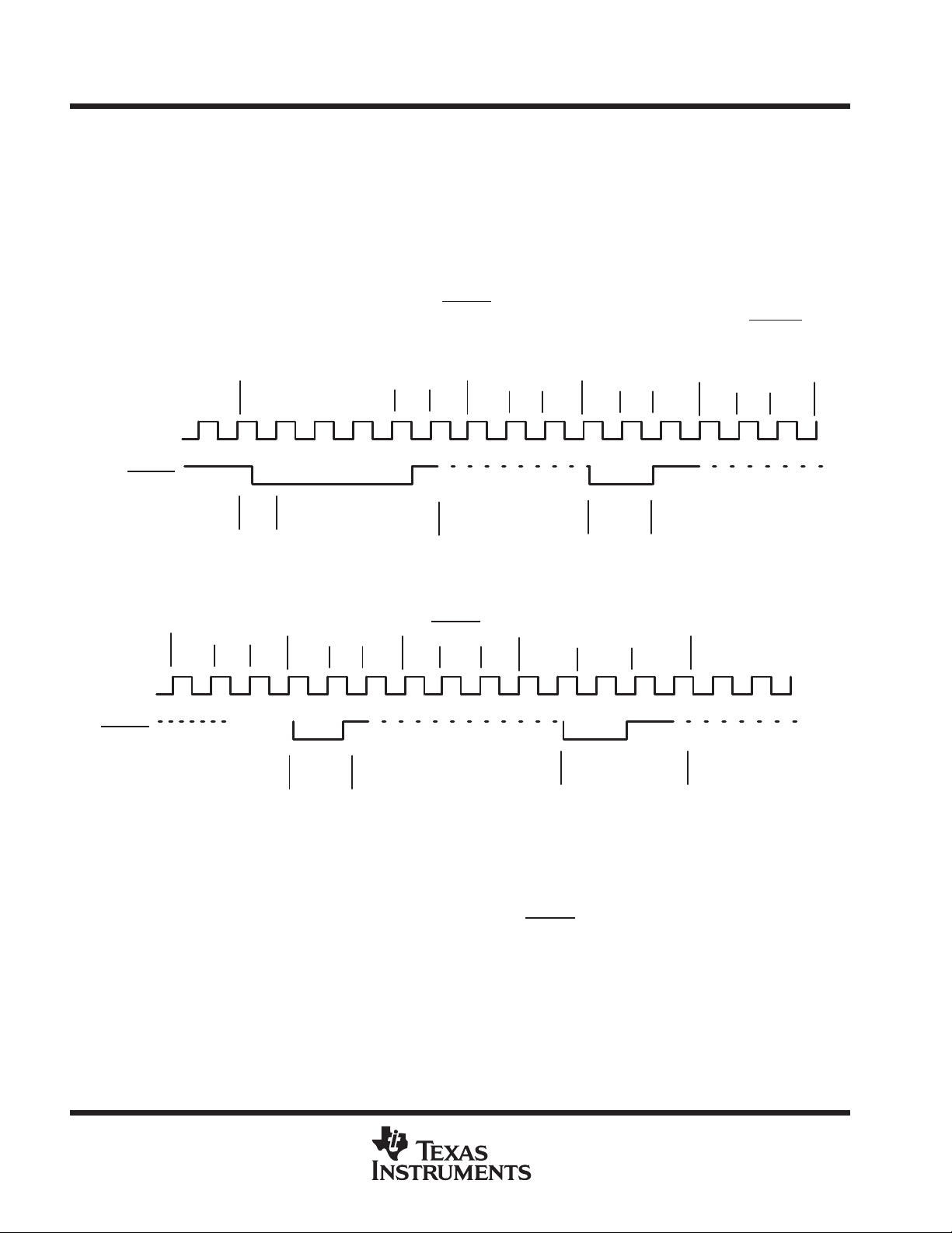
PCI1031
PCI-TO-PC CARD16 CONTROLLER UNIT
SCPS008B – FEBRUARY 1996 – REVISED DECEMBER 1997
serialized IRQ signaling
The serialized interrupt protocol implemented in the PCI1031 uses a single PCI1031 terminal to communicate
all interrupt status information to the host interrupt controller. The protocol defines a serial packet consisting of
a start cycle, a stop cycle, and multiple interrupt cycles. All data in the packet is synchronous with PCLK. The
duration of the stop and interrupt cycles is a fixed number of clock periods, but the start cycle is variable (four
to eight clock periods). This allows the serial packet to retain coherence on either side of a PCI-to-PCI bridge.
Figures 4 and 5 illustrate how the serialized IRQ protocol works. Figure 4 shows the start cycle and the first
several IRQ sampling periods, and Figure 5 shows the final IRQ sampling periods and the stop cycle. The
intermediate IRQ sampling periods are not shown, but the sampling periods occur in ascending IRQ order:
IRQ0, IRQ1, SMI, IRQ3, IRQ4 . . . IRQ15, and IOCHK
illustrations, IRQ1 and IRQ15 are sampled deasserted. The stop cycle only can occur after the IOCHK period,
but can be extended to allow more sampling periods for platform-specific functions.
Start Cycle
. The IRQ signals are active high. In the following
IRQ0 IRQ1
SMI (IRQ2)
PCLK
IRQSER
Drive Source
PCLK
IRQSER
Drive Source
IRQx
H
Start
Host Controller
H = Host Control; R = Recovery; T = Turnaround; S = Sample
RT
S RT
None None
S RT
IRQ1
not
asserted
Figure 4. Serial-Interrupt Timing – Start Cycle and IRQ Sampling Periods
IRQ14 IRQ15
S
RT
None
H = Host Control; R = Recovery; T = Turnaround; S = Sample
S
IRQ15
not
asserted
RT
IOCHCK
S RT
None
STOP
H
Stop
Host Controller
RT
Figure 5. Serial-Interrupt Timing – Stop Cycle
S RT
None
In a system using the serialized IRQ protocol, the host software must configure the PCI1031 to use serialized
IRQs by setting bits 2–1 of the PCI configuration register at offset 92h to 10b. The step-by-step series of events
that host software must follow to successfully configure the PCI1031 for serialized IRQ signaling follows. These
steps assume that the system has powered up, PCI reset, and RSTIN
is high (deasserted). In cases where only
select bits of a register are to be modified, host software must leave the remaining register bits unchanged by
reading the current contents of the register first, modifying the desired bits, then writing the new value back to
the register.
26
POST OFFICE BOX 655303 • DALLAS, TEXAS 75265
Page 27

PCI-TO-PC CARD16 CONTROLLER UNIT
SCPS008B – FEBRUARY 1996 – REVISED DECEMBER 1997
serialized IRQ signaling (continued)
1. Set bits 2–1 of PCI device control register 92h (function 0) to 10b.
2. Write to the upper nibble of ExCA register 05h/45h/805h for desired CSC routing for each socket (all 15 IRQs
are available for routing when serialized IRQ signaling has been selected).
3. If a PC Card is installed in the socket and requires functional interrupts, write to the lower nibble of ExCA
register 03h/43h/803h for desired functional interrupt routing for the socket.
4. Using T able 8, write to the appropriate mask register bits to enable interrupt generation for desired events.
5. On card-removal events, host software should unroute any functional interrupts that were set for that
socket.
6. Upon card-insertion events, host software should reconfigure the mask and routing registers to support the
new card requirements.
PCI clock run
PCI1031
The PCI1031 supports PCI clock run (CLKRUN
determine the status of CLK as an open-drain output to request the CLK to restart or to speed up. PCI CLKRUN
is enabled by setting bit 0 in the system control register (see
resource manager informs the PCI1031 that the PCI clock is stopped or slowed, the PCI1031 ensures that no
transactions are in progress for either of the two PC Card sockets before allowing the clock resource manager
to stop or slow the PCI clock. CLKRUN
information on configuring the clock run option.
CLKRUN configuration
Bits 1–0 in the TI extension registers at offset 80h are used to enable and configure CLKRUN. Bit 0 enables
CLKRUN. Bit 1, when set, keeps the PCI clock running in response to a PCI CLKRUN deassertion (see
control register
conditions for stopping/slowing the PCI clock
Before allowing the central resource to slow or stop the PCI clock, the following conditions are checked:
D
The PCI CLKRUN enable bit is set and the KEEP CLOCK bit is cleared (see
D
Neither socket is in the process of powering up or powering down.
D
The 16-bit resource managers are not busy.
D
The PCI master is not busy.
D
No socket interrogation is underway.
D
No card interrupts are pending.
conditions for restarting the PCI clock
The PCI clock restarts when any PC Card is installed in a socket or removed from a socket. For 16-bit cards,
if the PCI clock stops or slows, the PCI1031 requests that the clock be restarted under the following conditions:
).
shares the IRQ10 pin on the PCI1031. See
). CLKRUN is an optional signal that is used as an input to
system control register
). When the PCI clock
system control register
system control register, bit 1
for
system
).
D
A 16-bit I/O card asserts IREQ.
D
A 16-bit I/O card asserts STSCHG/RI.
D
A 16-bit DMA card asserts DREQ.
POST OFFICE BOX 655303 • DALLAS, TEXAS 75265
27
Page 28
PCI1031
PCI-TO-PC CARD16 CONTROLLER UNIT
SCPS008B – FEBRUARY 1996 – REVISED DECEMBER 1997
PC Card DMA and distributed DMA
DMA is a concept with many different interpretations and implementations, depending on the context and
application. In fact, DMA support within the PCI1031 has different connotations, depending on whether the
subject is PCI or PC Card DMA. On the PC Card side, the PCI1031 supports the DMA protocol defined in the
1995 PC Card standard on both sockets. On the PCI side, the PCI1031 supports a distributed DMA protocol,
compliant with the distributed DMA on the PCIWay, revision 6.0, specification. It also supports PC/PCI DMA in
systems designed with the Intel MPIIX.
DMA on PCI is accomplished by compliance with the distributed DMA specification. The PCI1031 complies with
this specification as it applies to DMA devices, and implements two DMA channels; one per socket. Each DMA
channel is controlled by the host via a 16-byte window in PCI I/O address space. This window is mapped in
internal PCI1031 registers that are similar to the 8237 DMA controller programming model. By programming
these registers, the PCI1031 services DMA requests from PC Card applications by initiating PCI bus mastering
cycles to host memory address space.
DMA configuration
Host software must program the PCI1031 socket DMA registers 0 and 1 to set up the socket for DMA transfers.
These registers are found in the PCI configuration header, offsets 94h and 98h (see
DMA register 0
). Socket DMA register 0 applies to the PC Card portion of DMA transfers. Socket DMA register 1
applies to the PCI portion of DMA transfers and complies with the distributed DMA specification.
test register
and
socket
Socket DMA register 0 has only two significant bits. Bits1–0 encode the DREQ signal used by the PC Card. This
field must be programmed with a valid value before the PCI1031 initiates a DMA transfer. Socket DMA register 1
has 16 significant bits, and the encoding is shown in Table 9. The most important field in socket DMA register 1
is the base address that locates the DMA registers in PCI I/O address space. This is how the host communicates
and configures the DMA transfer process.
Table 9. Socket DMA Register 1
BIT TYPE FUNCTION
31–16 R Reserved. Bits 31–16 are read only and return 0s when read. Writes have no effect.
DMA base address. Bits 15–4 locate the socket DMA registers in PCI I/O space. This field represents a 16-bit PCI I/O
15–4 R/W
3 R Nonlegacy extended addressing. This is not supported on the PCI1031 and always returns a 0.
2–1 R/W
0 R/W
address. The upper 16 bits of the address are hardwired to 0, forcing this window to within the lower 64K bytes of I/O
address space. The lower four bits are hardwired to 0, forcing the window to a natural 16-byte boundary.
Transfer size. Bits 2–1 specify the width of the DMA transfer on the PCI interface. This field is encoded as:
00 = 8-bit transfer (default)
01 = 16-bit transfer
10 = Reserved
11 = Reserved
Decode enable. Enables the decoding of the DMA base address by the PCI1031. Bit 0 is encoded as:
0 = Disabled (default)
1 = Enabled
When host software initializes the PCI1031, the base address in socket DMA register 1 can be programmed,
but not enabled. When a particular DMA-capable PC Card is installed in the socket, host software can proceed
to program the DREQ
signaling option, the datapath width, and enable the DMA register decode in I/O space.
These options are specific to the PC Card and must be set when the card is configured, but not when the socket
is configured. After setting these options and enabling the DMA register decode, the DMA registers can be
programmed. The DMA register programming model is shown in Table 10.
28
POST OFFICE BOX 655303 • DALLAS, TEXAS 75265
Page 29
Reserved
Page
00h
Reserved
Reserved
04h
Reserved
08h
Multichannel mask
Reserved
Reserved
0Ch
DMA configuration (continued)
PCI1031
PCI-TO-PC CARD16 CONTROLLER UNIT
SCPS008B – FEBRUARY 1996 – REVISED DECEMBER 1997
Table 10. DMA Registers
R/W REGISTER NAME
R
W
R
W
R NA
W Mode
R
W
Current address
Base address
Current word
Base word
NA Status
Request Command
NA
Master clear
DMA BASE
ADDRESS OFFSET
The DMA registers contain control and status information consistent with the 8237 DMA controller; however,
the register locations are reordered and expanded in some cases. Refer to
DMA registers
for a detailed
description of the individual bits contained in the DMA registers. While the DMA register definitions are identical
to those in the 8237 DMA controller of the same name, some register bits defined in the 8237 DMA controller
do not apply to distributed DMA in a PCI environment. In such cases, the PCI1031 implements these obsolete
register bits as read-only , nonfunctional bits. The reserved registers shown in T able 10 are implemented as read
only, and return 0s when read. Writes to reserved registers have no effect.
DMA transfers
The DMA transfer is prefaced by several configuration steps that are specific to the PC Card and must be
completed after the PC Card is inserted and interrogated, as follows:
1. Set the proper DMA request (DREQ) signal assignment in the PCI configuration, offset 94h (bits 1–0).
2. Set the proper data width of the DMA transfer in the PCI configuration, offset 98h (bits 2–1).
3. Enable I/O window decoding of the DMA registers by setting bit 0 in the PCI configuration offset 98h.
These steps assume that host software has already powered the PC Card, interrogated its CIS, and set the
appropriate bits in the PCI1031 that identify the card as a 16-bit I/O PC Card. Also, both I/O access and bus
mastering must be enabled in the PCI command register. Host software can then program the DMA registers
with the transfer count, direction of the transfer, and memory location of the data. Once this programming is
complete, the PCI1031 awaits the assertion of DREQ
to initiate the transfer.
DMA writes transfer data from the PC Card to PCI memory addresses. The PCI1031 accepts data 8 or 16 bits
at a time (depending on the programming of the data width register field), then requests access to the PCI bus
by asserting its REQ
signal. Once granted access to the bus and the bus returns to an idle state, the PCI1031
initiates a PCI memory write command to the current memory address and transfers the data in a single data
phase. After terminating the PCI cycle, the PCI1031 accepts the next byte(s) from the PC Card until the transfer
count expires.
DMA reads transfer data from PCI memory addresses to the PC Card application. Upon the assertion of DREQ,
the PCI1031 asserts its PCI REQ signal to request access to the PCI bus. Once access is granted and the bus
is idle, the PCI1031 initiates a PCI memory read operation to the current memory address and accepts 8 or
16 bits of data (depending on the programming of the socket DMA register 1 field). After terminating the PCI
cycle, the data is passed on to the PC Card. After terminating the PC Card cycle, the PCI1031 requests access
to the PCI bus again until the transfer count expires.
POST OFFICE BOX 655303 • DALLAS, TEXAS 75265
29
Page 30
PCI1031
PCI-TO-PC CARD16 CONTROLLER UNIT
SCPS008B – FEBRUARY 1996 – REVISED DECEMBER 1997
DMA transfers (continued)
PCI I/O read and write cycles to the DMA registers are accepted and serviced during DMA transfers. If, while
a DMA transfer is in progress, the host resets the DMA channel, the PCI1031 asserts TC and ends the PC Card
cycle(s). TC is indicated in the DMA status register. At the PC Card interface, the PCI1031 supports demand
mode transfers. The PCI1031 asserts DACK the entire duration of the transfer unless DREQ is high
(deasserted) before TC. There is no performance penalty for long wait states during this mode of operation as
there is in the legacy ISA system, because the DMA channel is a dedicated resource localized at the
PC Card socket.
PC/PCI DMA
The PC/PCI DMA protocol provides a way for legacy I/O devices to do DMA transfers on the PCI bus in systems
equipped with the Intel MPIIX. The Intel MPIIX supports PC/PCI DMA expansion for docking station applications
where I/O devices require DMA transfers between the docking station PCI bus or extended I/O bus and a PCI
bus in the notebook docking computer.
In the PC/PCI DMA protocol, the PCI1031 acts as a PCI slave device. The Intel MPIIX DMA controller uses
request/grant pairs, REQ
as the PCI1031. The Intel MPIIX REQ and GNT pins correspond to the PCI1031 IRQ7 and IRQ11 pins,
respectively . Under the PC/PCI protocol, a PCI DMA slave device requests a DMA transfer using a serialized
protocol on REQ. The Intel MPIIX, as a bus master , arbitrates for the PCI bus. When the Intel MPIIX gets control
of the PCI bus, it asserts GNT
memory cycles on the PCI bus.
[A–B] and GNT[A–B], which are configured to support a PCI DMA slave device such
on the PCI1031 and, for the selected DMA channel, runs the DMA I/O cycles and
PC/PCI DMA is enabled for each PC Card16 slot by setting bit 19 in the respective system control register (see
T able 16). On power up, bit 19 is cleared, disabling PC/PCI DMA. Bit 3 of each PCI1031 system control register
is a global PC/PCI enable bit. When bit 3 is set, the PCI1031 can request a DMA transfer by asserting IRQ7
(REQ) and encoding the channel request information using the serialized protocol. When the Intel MPIIX gets
control of the PCI bus, it encodes the granted channel on the PCI1031 IRQ11 (GNT) pin. On power up, bit 3
is cleared and PC/PCI DMA is disabled. When the PCI1031 receives a GNT
signal, it looks at the DMA I/O
address to determine the type of transfer. The cycle types are as follows:
DMA I/O ADDRESS DMA CYCLE TYPE TERMINAL COUNT PCI CYCLE TYPE
00h Normal 0 I/O read/write
04h Normal TC 1 I/O read/write
C0h Verify 0 I/O read
C4h Verify TC 1 I/O read
30
POST OFFICE BOX 655303 • DALLAS, TEXAS 75265
Page 31

DMA CHANNEL
PC/PCI DMA (continued)
To do PC/PCI DMA transfers, the following conditions must be met:
D
Bit 3 in the system control register must be set to enable the PCI1031 to do PC/PCI DMA transfers.
D
The desired DMA channel for each PC Card16 slot (slot A and slot B) must be configured via bits 18–16
in the respective system control register (see Table 16). The Intel MPIIX uses this channel to do the DMA
transfers. The channels are configured as follows:
BITS
18 17 16
0 0 0 Channel 0
0 0 1 Channel 1
0 1 0 Channel 2
0 1 1 Channel 3
1 0 0 Channel 4
1 0 1 Channel 5
1 1 0 Channel 6
1 1 1 Channel 7
PCI1031
PCI-TO-PC CARD16 CONTROLLER UNIT
SCPS008B – FEBRUARY 1996 – REVISED DECEMBER 1997
D
Each PC Card16 slot must be enabled by setting bit 19 of the respective system control register.
DMA channels 0–3 are used for 8-bit DMA transfers and channels 5–7 are used for 16-bit DMA transfers. On
power up, the system control register bits 18–16 default to 100 (channel 4). DMA channel 4 is used by PCI
master devices to request the bus; hence, PC/PCI DMA is not the default mode.
The REQ and GNT signal pairs can be configured to support slave devices on the primary bus (i.e., the same
bus as the Intel MPIIX) or slave devices on a secondary bus such as a PCI-to-ISA bridge. The REQ/GNT pairs
are configured by setting the PCI DMA expansion register (offset 088h and 089h, respectively). If the REQ
pairs are configured to support a slave device on a secondary bus, the signals must be properly routed to the
Intel MPIIX DMA controller, either through the docking station bridge chip or through the docking
station connector.
ring indicate
When a 16-bit I/O PC Card is inserted into a socket, the PCI1031 can be configured to allow a ring detect signal
to be passed from the PC Card to the system on the IRQ15/RI_OUT
the RI_OUT function on IRQ15 by setting bit 7 of the card control register (see
extension registers. Next, bit 7 of the ExCA interrupt and general control register (see
general control register
) of the ExCA registers must be set to enable the RI input for the 16-bit I/O PC Card to
support the RI function. When RI sees a low, it is passed through to the IRQ15/RI_OUT (see Figure 6). The
status of the RI
register
) of the ExCA registers.
input is reflected in bit 0 of the card status-change register (see
pin. This is accomplished by first enabling
card control register
ExCA interrupt and
ExCA card status-change
/GNT
) of the TI
POST OFFICE BOX 655303 • DALLAS, TEXAS 75265
31
Page 32

PCI1031
PCI-TO-PC CARD16 CONTROLLER UNIT
SCPS008B – FEBRUARY 1996 – REVISED DECEMBER 1997
ring indicate (continued)
PCI1031
A
RI
IRQ15/RI_OUT
RI
Figure 6. Ring Indicate Enabled on PCI1031
zoom video
The PCI1031 allows the implementation of the zoom video proposal before the PCMCIA. Zoom video is
supported by setting bit 6 of the card control register (see
Setting bit 6 puts address lines A25–A4 of the PC Card interface in the high-impedance state. These lines can
then be used to transfer video and audio data directly to the appropriate controller. Address lines A3–A0 can
still be used by the PCI1031 to access PC Card CIS registers for PC Card configuration (see Figure 7).
card control register
CARD A
B
CARD B
) in the TI extension registers.
PCI
Local Bus
VGA
Controller
ZV-Port
(video)
PCI1031
19
Motherboard
PCM
Audio
Input
Audio
Codec
4
SpeakersCRT
PC Card
Socket
PC Card
4
PCMCIA
Interface
19
Video and Control
Audio
Video
32
Figure 7. Zoom-Video Implementation on the PCI1031
POST OFFICE BOX 655303 • DALLAS, TEXAS 75265
Page 33

PCI-TO-PC CARD16 CONTROLLER UNIT
SCPS008B – FEBRUARY 1996 – REVISED DECEMBER 1997
power management
The PCI1031 provides four methods of power management. These methods relate to the primary bus (PCI) and
the secondary bus. Managing the PCI clock is the main method of conserving power on the PCI1031.
PCI power management
The PCI clock run feature is the primary method of power management on the PCI bus side of the PCI1031.
To enable the PCI1031 to fit into the suspend and resume schemes of all the various chipsets, the PCI1031
implements SUSPEND that allows RSTIN (PCIRST) to be asserted as the system resumes, while preserving
the state of the PCI1031 internal registers.
PCI clock run
The PCI1031 supports the PCI clock run protocol as defined in the PCI mobile design guide revision 1.0. When
the system’s central resource signals the system to stop the PCI clock by driving CLKRUN
either signals that it is acceptable to stop the PCI clock by not driving CLKRUN or signals to the system to keep
the clock running by pulling CLKRUN low.
The PCI1031 CLKRUN is multiplexed on the IRQ10 interrupt line. The PCI1031 clock run feature is enabled
by setting bit 0 in the system control register, 80h (see
clock run functionality of the multiplexed pin IRQ10/CLKRUN. Bit 1 of the system control register allows software
to enable the PCI1031 keep clock running mode to prevent the system from stopping the PCI clock. When bit
1 of the system control register is set, the PCI1031 signals back to the system to keep the PCI clock running
(not stop the clock). Figure 8 shows a diagram of the PCI bus clock states and the logic level of CLKRUN
each state.
system control register
). Bit 0 enables/disables the PCI
high, the PCI1031
PCI1031
for
The PCI1031 signals the system to restart the clock when one of the following events occurs:
D
A card is inserted or removed. The PCI1031 signals to start the PCI clock and generates a card
status-change interrupt on the CSC interrupt routing.
D
A functional interrupt is generated by a PC Card. The PCI1031 signals to start the PCI clock and generates
a functional interrupt on the appropriate routing.
D
A ring indicate (RI) signal is detected by PC Card16. The PCI1031 signals to start the PCI clock and a ring
indicate output (RI_OUT
) signal is provided to the system.
POST OFFICE BOX 655303 • DALLAS, TEXAS 75265
33
Page 34

PCI1031
PCI-TO-PC CARD16 CONTROLLER UNIT
SCPS008B – FEBRUARY 1996 – REVISED DECEMBER 1997
PCI clock run (continued)
Bus Busy
(CLKRUN
low)
Clock
Running
PCI1031 Clock Continue (CLKRUN
low)
Bus Idle (CLKRUN
Four PCI Clocks Minimum
high)
Clock
Stop/Slow
Request
Clock
Stopped/
Slowed
(CLKRUN
high)
CardBus Clock Running
Stop CardBus Clock (CLKRUN
PCI1031 Clock Restart (CLKRUN
low)
low)
Figure 8. Clock Run and Bus States
PCI suspend/resume
The PCI1031 implements a suspend feature that allows (RSTIN) to be asserted without resetting the PCI1031
internal registers. SPKROUT is multiplexed with SUSPEND. The multiplex control is provided in the PCI
configuration space by setting bit 1 of the card control register, 92h (see
card control register
). Some chipsets
provide a PCIRESET signal that is asserted when the system resumes after a suspend period. With these
particular chipsets, the PCI1031 suspend feature must be implemented to allow the system to activate suspend
without clearing the internal registers on the PCI1031 (see Figure 9). If a chipset does not require suspend,
SUSPEND
can be pulled high or SPKROUT can be activated. The default state for SUSPEND is active.
Any bus contention between SPKROUT and SUSPEND is avoided because the PCI1031 implements a
three-PCI-clock-cycle delay after the control bit in the card control register is changed. This allows the pullup
resistor on the pin to pull the line high so that an erroneous suspend mode does not occur.
34
POST OFFICE BOX 655303 • DALLAS, TEXAS 75265
Page 35

PCI suspend/resume (continued)
PCI1031
PCI-TO-PC CARD16 CONTROLLER UNIT
SCPS008B – FEBRUARY 1996 – REVISED DECEMBER 1997
Power Up Active Suspend Active
Needs SUSPEND
Does Not Need SUSPEND
PCIRESET
SUSPEND
NotOnResume
SUSPEND (high)
Figure 9. PCI Reset and Suspend Mode
PC Card16 mode
When a 16-bit legacy PC Card is inserted into a socket, there are two options for minimizing power consumption.
The first is to use the card output enable (COE) bit (see bit 7 of the
ExCA power control register
). When bit 7
is set, the outputs on the PC Card socket are placed in the high-impedance state. Bit 7 is software controlled.
Socket services must clear bit 7 to activate the socket. The second method is to set the power-down bit (see
bit 0 of the
ExCA global control register
). When bit 0 is set, it enables an automated COE bit. When a card access
to a PC Card16 card is complete, the PCI1031 automatically places the card outputs in the high-impedance
state. When there is any activity on the socket, the outputs are automatically enabled.
The major difference between the use of the COE bit and the POWERDWN bit is that the COE bit resets the
PC Card16 PC Card and the POWERDWN bit does not. The POWERDWN bit continues to drive the Card
RESET line inactive, while the COE bit puts the RESET line in the high-impedance state.
PCI configuration header registers
A number of registers found in the PCI1031 PCI configuration space are defined in the PCI-to-PCI bridge
architecture specification revision 1.0, which, in turn, are common to the PCI local bus specification revision 2.1.
Registers common to both specifications are the device ID, vendor ID, status, command, class code, revision
ID, BIST, header type, latency timer, cache line size, interrupt pin, and interrupt line registers.
The following PCI specific registers listed in the previous paragraph are applicable to the entire device and are
not specific to any one PCI function (i.e., PC Card socket) on the PCI1031. These registers include the
device ID, vendor ID, status, command, class code, revision ID, BIST, header type, latency timer, cache line
size, interrupt pin, and interrupt line registers. Each register is mapped to the same location in both PCI
configuration spaces. Access is possible by addressing the configuration space of either function, but host
software should consistently access PCI specific registers through a single function. Detailed descriptions of
the PCI specific registers follow and are listed in T able 12. Most of the registers are implemented in the PCI1031
as defined in either the PCI local bus specification revision 2.1, the PCI-to-PCI bridge architecture specification
revision 1.0, or the Yenta specification revision 2.1. References to these documents are made where
appropriate. Additional register bits defined in the bridge control register (see
specific to CardBus memory windows.
POST OFFICE BOX 655303 • DALLAS, TEXAS 75265
bridge control
) enable features
35
Page 36

PCI1031
PCI-TO-PC CARD16 CONTROLLER UNIT
SCPS008B – FEBRUARY 1996 – REVISED DECEMBER 1997
PCI configuration headers (continued)
Host software exerts control and retrieves status information on PC Cards via a standard set of internal PCI1031
registers: ExCA registers for 16-bit PC Cards. The PCI1031 maps these registers into PCI address space for
access by host software. The locations of these registers are set by the CardBus socket registers/ExCA
registers base address (see
configuration space, which locates a 4K-byte nonprefetchable memory window in PCI memory address space.
Within this memory window, the PCI1031 maps both the socket registers and the ExCA registers. Each socket
has a separate CardBus socket register/ExCA registers base address register for accessing the ExCA registers.
The 16-bit PC Cards use the ExCA register set for card status and control purposes. Traditionally, these
registers have been accessed by host software through an index/data register pair. Software would write the
index of the desired ExCA register to the index register, and read or write the desired data to the data register.
The PCI1031 departs from this scheme by directly mapping the ExCA register set to a 4K-byte memory window
located by the CardBus socket registers/ExCA registers base address register. The ExCA registers are of fset
from this base address by 800h. The PCI1031 also supports the index/data scheme of accessing the ExCA
registers through the use of the PC Card 16-bit I/F legacy-mode base address register (see
legacy-mode base address
the address+1 becomes the address for the data address. Using this access method, applications requiring
index/data type ExCA access can be supported. This PC Card 16-bit legacy-mode base address is shared by
both sockets and the ExCA registers run contiguously from offset 00h–3Fh for Socket A and 40h–7Fh for
socket B.
CardBus socket registers/ExCA registers base address register
) register in PCI
PC Card 16-bit I/F
). An address written to this register becomes the address for the index register and
The PCI1031 implements two PCI configuration headers, one for each PC Card socket; therefore, all memory
and I/O window functionality for socket A are repeated, but separate from, socket B. Host software must
program nonoverlapping memory and I/O resources for each socket.
The TI extension registers are specific PCI1031 value-added features that are not part of currently defined PC
Card industry specifications. The TI extension registers are a collection of control and status bits that are
required to support various PCI1031 functions. These functions typically do not exist within the register models
implemented elsewhere within the device. T ables 1 1 and 12 show the TI extension registers and their locations
in PCI configuration space.
Table 11. TI Extension Registers
REGISTER NAME OFFSET
System control
Retry status
Card control
Device control
†
Test
†
One or more bits in the register are
common to PCI functions 0 and 1.
†
†
†
†
80h
90h
91h
92h
93h
The PCI1031 supports the DMA specification defined in the 1995 PC Card standard by providing one DMA
channel per socket. The PC Card standard stipulates the signaling and timing associated with DMA transfers
to and from a PC Card. This defines DMA transfers from the PC Card to the socket only . On the PCI side, the
PCI1031 implements a set of status and control registers similar to the programming model of the original dual
8237 DMA controller found in PC-A T systems. These registers comply with the specification for distributed DMA
in a PCI environment, particularly as it defines DMA devices. The PCI1031 provides two registers in its
configuration header that set up both the PCI interface and PC Card socket for DMA. See
distributed DMA
for a complete discussion of DMA support on the PCI1031.
PC Card DMA
and
36
POST OFFICE BOX 655303 • DALLAS, TEXAS 75265
Page 37

PCI-TO-PC CARD16 CONTROLLER UNIT
SCPS008B – FEBRUARY 1996 – REVISED DECEMBER 1997
PCI configuration headers (continued)
Host software must program the PCI1031 socket DMA registers 0 and 1 to set up the socket for DMA transfers.
Socket DMA register 0 applies to the PC Card portion of DMA transfers. Socket DMA register 1 applies to the
PCI portion of DMA transfers specifically to set up the DMA support required in distributed DMA. Socket DMA
register 1 provides register bits to program the DMA transfer width. This transfer width refers to both the PC Card
interface and the PCI interface.
Descriptions of each of the registers follow. Before writing data to any of the TI extension registers, host software
must first read the register to preserve the current contents. After reading the register, software can modify the
desired bits and write back the new data. This preserves current register settings and prevents unpredictable
or undesirable behavior.
The PCI1031 configuration header is shown in Table 12.
Table 12. PCI1031 Configuration Header
REGISTER NAME OFFSET
Device ID Vendor ID 00h
Status Command 04h
Class code Revision ID 08h
BIST Header type Latency timer
CardBus socket registers/ExCA base-address register 10h
Secondary status (unused)
CardBus latency timer
†
Test
†
One or more bits in the register are common to PCI functions 0 and 1.
‡
Unused registers are read only.
†
Bridge control
Subsystem ID Subsystem vendor ID 40h
Subordinate bus number CardBus bus number PCI bus number
‡
CardBus memory base register 0 (unused)
CardBus memory limit register 0 (unused)
CardBus memory base register 1 (unused)
CardBus memory limit register 1 (unused)
CardBus I/O base register 0 (unused)
CardBus I/O limit register 0 (unused)
CardBus I/O base register 1 (unused)
CardBus I/O limit register 1 (unused)
†
PC Card 16-Bit I/F legacy-mode base address
Reserved 48h–7Ch
System control
Reserved 84h–8Ch
Device control
†
Socket DMA register 0 94h
Socket DMA register 1 98h
Reserved 9Ch–FFh
†
Reserved 14h
‡
‡
‡
‡
‡
‡
‡
‡
Interrupt pin Interrupt line 3Ch
†
†
Card control
†
Cache line size
Retry status
†
†
†
PCI1031
0Ch
18h
1Ch
20h
24h
28h
2Ch
30h
34h
38h
44h
80h
90h
POST OFFICE BOX 655303 • DALLAS, TEXAS 75265
37
Page 38

PCI1031
PCI-TO-PC CARD16 CONTROLLER UNIT
SCPS008B – FEBRUARY 1996 – REVISED DECEMBER 1997
PCI vendor ID register
Bit 15 14 13 12 11 10 9 8 7 6 5 4 3 2 1 0
Name PCI vendor ID
Type R R R R R R R R R R R R R R R R
Default 0 0 0 1 0 0 0 0 0 1 0 0 1 1 0 0
Register: PCI vendor ID
Type: Read only
Offset: 00h
Default: 104Ch
Description: This 16-bit value is allocated by the PCI special interest group (SIG) and identifies TI as the
manufacturer of this device. The vendor ID assigned to TI is 104Ch.
PCI device ID register
Bit 15 14 13 12 11 10 9 8 7 6 5 4 3 2 1 0
Name PCI device ID
Type R R R R R R R R R R R R R R R R
Default 1 0 1 0 1 1 0 0 0 0 0 1 0 0 1 1
Register: PCI device ID
Type: Read only
Offset: 02h
Default: AC13h
Description: This 16-bit value is allocated by the vendor. The device ID for the PCI1031 is AC13h.
PCI command register
Bit 15 14 13 12 11 10 9 8 7 6 5 4 3 2 1 0
Name PCI command
Type R R R R R R R R/W R R/W R R R R/W R/W R/W
Default 0 0 0 0 0 0 0 0 0 0 0 0 0 0 0 0
Register: PCI command
Type: Read only, read/write (see individual bit descriptions)
Offset: 04h
Default: 0000h
Description: The PCI command register provides control over the PCI1031’s ability to generate and
respond to PCI cycles. In its default state, or when 0000h is written, the PCI1031 can respond
to PCI configuration cycles only; all other PCI functionality is disabled. The PCI1031 does not
claim PCI cycles as a target, nor request access to the bus as an initiator in this state. Refer to
Table 13 for a complete description of the register contents.
38
POST OFFICE BOX 655303 • DALLAS, TEXAS 75265
Page 39

T able 13. PCI Command Register
BIT TYPE FUNCTION
15–10 R Reserved. Bits 15–10 are read only and return 0s when read.
9 R
8 R/W
7 R
6 R/W
5 R
4 R
3 R
2 R/W
1 R/W
0 R/W
Fast back-to-back enable. Bit 9 indicates whether the device is enabled for the fast back-to-back transaction function. The
PCI1031 does not support fast back-to-back PCI cycles. Bit 9 is read only and returns 0s when read.
System error (SERR) enable. Bit 8 and bit 6 must be set for the PCI1031 to report address parity errors.
Wait cycle control. Bit 7 indicates whether a PCI device is capable of address/data stepping. The PCI1031 does not
support address/data stepping; therefore, bit 7 is hardwired to 0. Bit 7 is read only and returns 0s when read. Writes to
bit 7 have no effect.
Parity error response. Data parity errors are indicated by asserting PERR, while address parity errors are indicated by
asserting SERR
VGA palette snoop. Bit 5 controls how PCI devices handle accesses to VGA palette registers. The PCI1031 does not
support VGA palette snooping; therefore, bit 5 is hardwired to 0. Bit 5 is read only and returns 0s when read. Writes to
bit 5 have no effect.
Memory write and invalidate enable. Bit 4 controls whether a PCI initiator device can generate memory write and invalidate
commands. The PCI1031 controller uses memory-write commands instead of memory-write- and-invalidate commands;
therefore, bit 4 is hardwired to 0. Bit 4 is read only and returns 0s when read. Writes to bit 4 have no effect.
Special cycles. Bit 3 controls whether or not a PCI device ignores PCI special cycles. The PCI1031 does not monitor
special cycle operations; therefore, bit 3 is hardwired to 0. Bit 3 is read only and returns 0s when read. Writes to bit 3 have
no effect.
Bus initiator control. Bit 2 controls whether or not a PCI device can act as a PCI bus initiator. Bit 2 is used for distributed
DMA only.
Memory space control. Bit 1 controls whether or not a PCI device can claim cycles in PCI memory space.
I/O space control. Bit 0 controls whether or not a PCI device can claim cycles in PCI I/O space.
0 = Disable the SERR
1 = Enable the SERR
.
0 = PCI1031 ignores detected parity error (default)
1 = PCI1031 responds to detected parity errors
0 = Disables the PCI1031’s ability to generate PCI bus accesses (default)
1 = Enables the PCI1031’s ability to generate PCI bus accesses
0 = Disables the PCI1031’s response to memory space accesses (default)
1 = Enables the PCI1031’s response to memory space accesses
0 = Disables the PCI1031’s response to I/O space accesses (default)
1 = Enables the PCI1031’s response to I/O space accesses
output driver (default)
output driver
PCI1031
PCI-TO-PC CARD16 CONTROLLER UNIT
SCPS008B – FEBRUARY 1996 – REVISED DECEMBER 1997
PCI status register
Bit 15 14 13 12 11 10 9 8 7 6 5 4 3 2 1 0
Name PCI status
Type R/W R/W R/W R/W R/W R R R/W R R R R R R R R
Default 0 0 0 0 0 0 1 0 0 0 0 0 0 0 0 0
Register: PCI status
Type: Read only, read/write (see individual bit descriptions)
Offset: 06h
Default: 0200h
Description: The PCI status register provides PCI -related device information to the host system. Bits in this
register can be read normally; however, writes behave dif ferently. A bit in the status register is
reset when a 1 is written to that bit location; a 0 written to a bit location has no effect. Refer to
Table 14 for a complete description of the register contents.
POST OFFICE BOX 655303 • DALLAS, TEXAS 75265
39
Page 40

PCI1031
PCI-TO-PC CARD16 CONTROLLER UNIT
SCPS008B – FEBRUARY 1996 – REVISED DECEMBER 1997
Table 14. PCI Status Register
BIT TYPE FUNCTION
Parity error status
15 R/W
System error status
14 R/W
Initiator abort status
13 R/W
Target abort status. A target abort terminates a PCI1031 bus master transaction.
12 R/W
Target abort status. The PCI1031 target abort terminates a bus master transaction.
11 R/W
10–9 R
8 R/W
7 R Fast back-to-back capable. The PCI1031 cannot accept fast back-to-back transactions; therefore, bit 7 is hardwired to 0.
6 R User-definable feature (UDF) support. The PCI1031 does not support the UDF option; therefore, bit 6 is hardwired to 0.
5 R 66 MHz capable. The PCI1031 operates at a maximum frequency of 33 MHz; therefore, bit 5 is hardwired to 0.
4–0 R Reserved. Bits 4–0 are read only alnd return 0s when read. Writes have no effect.
Device select timing status. Bits 10–9 are encoded with the DEVSEL timing. These read-only bits are hardwired as 01b,
indicating a medium-speed device.
Data parity status
0 = PCI1031 does not detect a parity error (default).
1 = PCI1031 detects a parity error.
0 = PCI1031 does not generate a system error on the SERR
1 = PCI1031 generates a system error on the SERR
0 = A bus initiator abort does not terminate a bus initiator’s transaction (default).
1 = A bus initiator abort terminates a bus initiator’s transaction.
0 = A target abort does not terminate a PCI1031 bus master transaction (default).
1 = A target abort terminates a bus master transaction.
0 = A PCI1031 target abort does not terminate a bus master transaction (default).
1 = A PCI1031 target abort terminates a bus master transaction.
0 = No data parity errors occur (default).
1 = Data parity errors occur; the following conditions are met:
a. PERR
b. The agent that set the bit is the bus initiator during the transaction when the error occurred.
c. Parity error response (bit 6 in the command register) is enabled.
is asserted by the bus initiator or the bus initiator observed PERR asserted.
line (default).
line.
PCI revision ID register
Bit 7 6 5 4 3 2 1 0
Name PCI revision ID
Type R R R R R R R R
Default 0 0 0 0 0 0 0 0
Register: PCI revision ID
Type: Read only
Offset: 08h
Default: 02h
Description: The PCI revision ID register is selected by TI and indicates the silicon revision.
40
POST OFFICE BOX 655303 • DALLAS, TEXAS 75265
Page 41

PCI1031
PCI-TO-PC CARD16 CONTROLLER UNIT
SCPS008B – FEBRUARY 1996 – REVISED DECEMBER 1997
PCI class code register
Bit 23 22 21 20 19 18 17 16 15 14 13 12 11 10 9 8 7 6 5 4 3 2 1 0
Name PCI class code
Byte Base Class Sub class Programming Interface
Type R R R R R R R R R R R R R R R R R R R R R R R R
Default 0 0 0 0 0 1 1 0 0 0 0 0 0 1 0 1 0 0 0 0 0 0 0 0
Register: PCI class code
Type: Read only
Offset: 09h
Default: 060500h
Description: The PCI class code indicates that the PCI1031 is a bridge device (06h), a PCMCIA bridge
(05h), with 00h programming interface.
cache line size register
Bit 7 6 5 4 3 2 1 0
Name Cache line size
Type R/W R/W R/W R/W R/W R/W R/W R/W
Default 0 0 0 0 0 0 0 0
Register: Cache line size
Type: Read/write, nonfunctional
Offset: 0Ch
Default: 00h
Description: This register is nonfunctional.
PCI latency timer register
Bit 7 6 5 4 3 2 1 0
Name PCI latency timer
Type R/W R/W R/W R/W R/W R/W R/W R/W
Default 0 0 0 0 0 0 0 0
register: pci latency timer
Type: Read/write, nonfunctional
Offset: 0Dh
Default: 00h
Description: This register is nonfunctional.
PCI header-type register
Bit 7 6 5 4 3 2 1 0
Name PCI header type
Type R R R R R R R R
Default 1 0 0 0 0 0 1 0
Register: PCI header type
Type: Read only
Offset: 0Eh
Default: 82h
Description: The PCI header type register indicates that the PCI1031 uses a CardBus bridge configuration
header. It also identifies the PCI1031 as a multifunction device.
POST OFFICE BOX 655303 • DALLAS, TEXAS 75265
41
Page 42

PCI1031
PCI-TO-PC CARD16 CONTROLLER UNIT
SCPS008B – FEBRUARY 1996 – REVISED DECEMBER 1997
BIST register
Bit 7 6 5 4 3 2 1 0
Name BIST
Type R R R R R R R R
Default 0 0 0 0 0 0 0 0
Register: BIST
Type: Read only
Offset: 0Fh
Default: 00h
Description: The PCI1031 does not support built-in self test (BIST); therefore, this register is considered
reserved. The BIST register is read only and returns 0s when read. Writes to this register have
no effect.
CardBus socket registers/ExCA base-address register
Bit 31 30 29 28 27 26 25 24 23 22 21 20 19 18 17 16
Name CardBus socket registers/ExCA base-address register
Type R/W R/W R/W R/W R/W R/W R/W R/W R/W R/W R/W R/W R/W R/W R/W R/W
Default 0 0 0 0 0 0 0 0 0 0 0 0 0 0 0 0
Bit 15 14 13 12 11 10 9 8 7 6 5 4 3 2 1 0
Name CardBus socket registers/ExCA base-address register
Type R/W R/W R/W R/W R R R R R R R R R R R R
Default 0 0 0 0 0 0 0 0 0 0 0 0 0 0 0 0
Register: CardBus socket registers/ExCA base-address register
Type: Read only, read/write
Offset: 10h
Default: 0000 0000h
Description: This register points to the nonprefetchable memory window where the PCI1031 maps both
the CardBus socket registers and the ExCA registers. The register is separated into two fields.
Bits 31–12 are read/write and allow the CardBus socket registers/ExCA registers to be
located anywhere in the 32-bit PCI I/O address space on 4K-byte boundaries. Bits 1 1–0 are
read only and are hardwired to 0 to indicate that this register represents a memory base
address. When software writes a value of all 1s to this register, the value read back is
FFFF F000h, indicating that at least 4K bytes of memory address space are required.
NOTE:
ExCA status and control registers start at offset 000h and the 16-bit card registers begin at
offset 800h.
secondary status register
Bit 15 14 13 12 11 10 9 8 7 6 5 4 3 2 1 0
Name Secondary status
Type R/W R/W R/W R/W R/W R R R/W R R R R R R R R
Default 0 0 0 0 0 0 1 0 0 0 0 0 0 0 0 0
Register: Secondary status
Type: Read only, read/write, not used
Offset: 16h
Default: 0200h
Description: This register is read only and is not used. Reads return 0s, writes have no effect.
42
POST OFFICE BOX 655303 • DALLAS, TEXAS 75265
Page 43

PCI1031
PCI-TO-PC CARD16 CONTROLLER UNIT
SCPS008B – FEBRUARY 1996 – REVISED DECEMBER 1997
PCI bus number register
Bit 7 6 5 4 3 2 1 0
Name PCI bus number
Type R/W R/W R/W R/W R/W R/W R/W R/W
Default 0 0 0 0 0 0 0 0
Register: PCI bus number
Type: Read/write, nonfunctional
Offset: 18h
Default: 00h
Description: This register is nonfunctional.
CardBus bus number register
Bit 7 6 5 4 3 2 1 0
Name CardBus bus number
Type R/W R/W R/W R/W R/W R/W R/W R/W
Default 0 0 0 0 0 0 0 0
Register: CardBus bus number
Type: Read/write, nonfunctional
Offset: 19h
Default: 00h
Description: This register is nonfunctional.
subordinate bus number register
Bit 7 6 5 4 3 2 1 0
Name Subordinate bus number
Type R/W R/W R/W R/W R/W R/W R/W R/W
Default 0 0 0 0 0 0 0 0
Register: Subordinate bus number
Type: Read/write, nonfunctional
Offset: 1Ah
Default: 00h
Description: This register is nonfunctional.
CardBus latency timer register
Bit 7 6 5 4 3 2 1 0
Name CardBus latency timer
Type R/W R/W R/W R/W R/W R/W R/W R/W
Default 0 0 0 0 0 0 0 0
Register: CardBus latency timer
Type: Read/write, nonfunctional
Offset: 1Bh
Default: 00h
Description: This register is nonfunctional.
POST OFFICE BOX 655303 • DALLAS, TEXAS 75265
43
Page 44

PCI1031
PCI-TO-PC CARD16 CONTROLLER UNIT
SCPS008B – FEBRUARY 1996 – REVISED DECEMBER 1997
memory base registers 0, 1
Bit 31 30 29 28 27 26 25 24 23 22 21 20 19 18 17 16
Name Memory base registers 0, 1
Type R R R R R R R R R R R R R R R R
Default 0 0 0 0 0 0 0 0 0 0 0 0 0 0 0 0
Bit 15 14 13 12 11 10 9 8 7 6 5 4 3 2 1 0
Name Memory base registers 0, 1
Type R R R R R R R R R R R R R R R R
Default 0 0 0 0 0 0 0 0 0 0 0 0 0 0 0 0
Register: Memory base registers 0, 1
Type: Read only, nonfunctional
Offset: 1Ch, 24h
Default: 0000 0000h
Description: The memory base registers are nonfunctional.
memory limit registers 0, 1
Bit 31 30 29 28 27 26 25 24 23 22 21 20 19 18 17 16
Name Memory limit registers 0, 1
Type R R R R R R R R R R R R R R R R
Default 0 0 0 0 0 0 0 0 0 0 0 0 0 0 0 0
Bit 15 14 13 12 11 10 9 8 7 6 5 4 3 2 1 0
Name Memory limit registers 0, 1
Type R R R R R R R R R R R R R R R R
Default 0 0 0 0 0 0 0 0 0 0 0 0 0 0 0 0
Register: Memory limit registers 0, 1
Type: Read only
Offset: 20h, 28h
Default: 0000 0000h
Description: The memory limit registers are nonfunctional.
I/O base registers 0, 1
Bit 31 30 29 28 27 26 25 24 23 22 21 20 19 18 17 16
Name I/O base registers 0, 1
Type R R R R R R R R R R R R R R R R
Default 0 0 0 0 0 0 0 0 0 0 0 0 0 0 0 0
Bit 15 14 13 12 11 10 9 8 7 6 5 4 3 2 1 0
Name I/O base registers 0, 1
Type R R R R R R R R R R R R R R R R
Default 0 0 0 0 0 0 0 0 0 0 0 0 0 0 0 0
Register: I/O base registers 0, 1
Type: Read only
Offset: 2Ch, 34h
Default: 0000 0000h
Description: This register is not used.
44
POST OFFICE BOX 655303 • DALLAS, TEXAS 75265
Page 45

PCI1031
PCI-TO-PC CARD16 CONTROLLER UNIT
SCPS008B – FEBRUARY 1996 – REVISED DECEMBER 1997
I/O limit registers 0, 1
Bit 31 30 29 28 27 26 25 24 23 22 21 20 19 18 17 16
Name I/O limit registers 0, 1
Type R R R R R R R R R R R R R R R R
Default 0 0 0 0 0 0 0 0 0 0 0 0 0 0 0 0
Bit 15 14 13 12 11 10 9 8 7 6 5 4 3 2 1 0
Name I/O limit registers 0, 1
Type R R R R R R R R R R R R R R R R
Default 0 0 0 0 0 0 0 0 0 0 0 0 0 0 0 0
Register: I/O limit registers 0, 1
Type: Read only
Offset: 30h, 38h
Default: 0000 0000h
Description: This register is not used.
interrupt line register
Bit 7 6 5 4 3 2 1 0
Name Interrupt line
Type R/W R/W R/W R/W R/W R/W R/W R/W
Default 1 1 1 1 1 1 1 1
Register: Interrupt line
Type: Read/write
Offset: 3Ch
Default: FFh
Description: The contents of this register default to the FFh (the unknown condition).
interrupt pin register
Bit 7 6 5 4 3 2 1 0
Name Interrupt pin
Type R R R R R R R R
Function 0 (socket A) default 0 0 0 0 0 0 0 1
Function 1 (socket B) default 0 0 0 0 0 0 1 0
Register: Interrupt pin
Type: Read only
Offset: 3Dh
Default: 01h for function 0 (socket A) and 02h for function 1 (socket B)
Description: This register is hardwired and writes to the register have no effect. The return values for the
register are 01h for function 0 (socket A) and 02h for function 1 (socket B).
POST OFFICE BOX 655303 • DALLAS, TEXAS 75265
45
Page 46

PCI1031
PCI-TO-PC CARD16 CONTROLLER UNIT
SCPS008B – FEBRUARY 1996 – REVISED DECEMBER 1997
bridge control register
Bit 15 14 13 12 11 10 9 8 7 6 5 4 3 2 1 0
Name Bridge control
Type R R R R R R/W R/W R/W R/W R/W R/W R R/W R/W R/W R/W
Default 0 0 0 0 0 0 1 1 0 1 0 0 0 0 0 0
Register: Bridge control
Type: Read only, read/write (see individual bit descriptions)
Offset: 3Eh
Default: 0340h
Description: This register provides control over PCI1031 bridging functions. Refer to Table 15 for a
complete description of the register contents.
Table 15. Bridge Control Register
BIT TYPE FUNCTION
15–1 1 R Reserved. Bits 15–11 are read only and return 0s when read. W rites have no effect.
Write posting enable. Enables posting of write data to and from the socket. If bit 10 is not set, the bridge must drain any
data in its buffers before accepting data for or from the socket. Each data word must then be accepted by the target before
10 R/W
9 R/W Memory window 1 type (nonfunctional)
8 R/W Memory window 0 type (nonfunctional)
7 R/W
6 R/W CardBus reset (nonfunctional)
5 R/W
4 R Reserved. Bit 4 is read only and returns 0, when read. Writes have no effect.
3 R/W
2 R/W Reserved. Bit 2 is nonfunctional.
1 R/W SERR enable (nonfunctional)
0 R/W Parity error response enable (nonfunctional)
the bridge can accept the next word from the source master. The bridge must not release the source master until the last
word is accepted by the target. Operating with write posting disabled inhibits system performance. Bit 10 is encoded as:
PCI interrupt-IREQ routing enable bit. When bit 7 is 0 and the PCI interrupt bit in device control register (see
register
7 is 1, the functional card interrupt is routed to an IRQ pin using the routing selected in the ExCA card interrupt and general
control register (see
Master abort mode. Bit 5 controls how the PCI1031 responds to a master abort when the PCI1031 is a master. Bit 5 is
common between each socket. Bit 5 is encoded as:
VGA enable. Bit 3 affects how the PCI1031 responds to VGA addresses. Bit 3 is encoded as:
0 = Write posting is disabled (default).
1 = Write posting is enabled.
) is enabled, the functional card interrupts are routed to the PCI interrupt for the socket (INTA or INTB). When bit
ExCA interrupt and general control register
0 = Functional interrupts are routed to PCI interrupts (default).
1 = Functional interrupts are routed by ExCA registers.
0 = Master aborts not reported (default)
1 = Signal target abort and SERR
0 = Normal operation. Accesses to VGA addresses are forwarded (default).
1 = Accesses to VGA addresses are not forwarded.
, if enabled
). Bit 7 is encoded as:
device control
46
POST OFFICE BOX 655303 • DALLAS, TEXAS 75265
Page 47

PCI1031
PCI-TO-PC CARD16 CONTROLLER UNIT
SCPS008B – FEBRUARY 1996 – REVISED DECEMBER 1997
subsystem vendor ID register
Bit 15 14 13 12 11 10 9 8 7 6 5 4 3 2 1 0
Name Subsystem vendor ID
Type R/W R/W R/W R/W R/W R/W R/W R/W R/W R/W R/W R/W R/W R/W R/W R/W
Default 0 0 0 0 0 0 0 0 0 0 0 0 0 0 0 0
Register: Subsystem vendor ID
Type: Read/write
Offset: 40h
Default: 0000h
Description: This register is read/write.
subsystem ID register
Bit 15 14 13 12 11 10 9 8 7 6 5 4 3 2 1 0
Name Subsystem ID
Type R/W R/W R/W R/W R/W R/W R/W R/W R/W R/W R/W R/W R/W R/W R/W R/W
Default 0 0 0 0 0 0 0 0 0 0 0 0 0 0 0 0
Register: Subsystem ID
Type: Read/write
Offset: 42h
Default: 0000h
Description: This register is read/write.
PC Card 16-bit I/F legacy-mode base address register
Bit 31 30 29 28 27 26 25 24 23 22 21 20 19 18 17 16
Name PC Card 16-bit I/F legacy-mode base address
Type R/W R/W R/W R/W R/W R/W R/W R/W R/W R/W R/W R/W R/W R/W R/W R/W
Default 0 0 0 0 0 0 0 0 0 0 0 0 0 0 0 0
Bit 15 14 13 12 11 10 9 8 7 6 5 4 3 2 1 0
Name PC Card 16-bit I/F legacy-mode base address
Type R/W R/W R/W R/W R/W R/W R/W R/W R/W R/W R/W R/W R/W R/W R R
Default 0 0 0 0 0 0 0 0 0 0 0 0 0 0 0 1
Register: PC Card 16-bit I/F legacy-mode base address
Type: Read only, read/write
Offset: 44h
Default: 0000 0001h
Description: The PCI1031 supports the index/data scheme of accessing the ExCA registers through the
use of the PC Card 16-bit I/F legacy-mode base-address register. An address written to this
register becomes the address for the index register and the address+1 becomes the address
for the data address. Using this access method, applications requiring index/data type ExCA
access can be supported.
POST OFFICE BOX 655303 • DALLAS, TEXAS 75265
47
Page 48

PCI1031
PCI-TO-PC CARD16 CONTROLLER UNIT
SCPS008B – FEBRUARY 1996 – REVISED DECEMBER 1997
system control register
Bit 31 30 29 28 27 26 25 24 23 22 21 20 19 18 17 16
Name System control
Type R R R R R R/W R/W R/W R R R/W R/W R/W R/W R/W R/W
Default 0 0 0 0 0 0 0 0 0 0 0 0 0 0 0 0
Bit 15 14 13 12 11 10 9 8 7 6 5 4 3 2 1 0
Name System control
Type R R R R R R R R R R R/W R/W R/W R/W R/W R/W
Default 0 0 0 0 X X X X 0 0 0 0 0 0 0 0
Register: System control
Type: Read only, read/write (see individual bit descriptions)
Offset: 80h
Default: 0004 1X00h
Description: The system control register provides status and control for system functions unique to
the PCI1031. Refer to Table 16 for a complete description of the register contents.
Table 16. System Control Register
BIT TYPE FUNCTION
31–27 R Reserved. Bits 31–27 are read only and return 0s when read.
System maintenance interrupt (SMI) routing selected. This is a global bit. Bit 26 is encoded as:
26 R/W
SMI interrupt status bit. Bit 25 is set to 1 when a write to either CardBus or ExCA power control for the socket and the SMI
25 R/W
24 R/W
23–22 R Reserved. Bits 23–22 are read only and return 0s when read.
21 R/W
20 R/W
19 R/W
18–16 R/W
15–14 R Reserved. Bits 15–14 are read only and return 0s when read.
13 R
interrupt mode is enabled in bit 24. Writing a 1 to bit 25 clears the status bit. Bit 25 is encoded as:
SMI interrupt mode enable. When enabled, SMI interrupts are generated when a write to the socket power control occurs.
This is a global bit. Bit 24 is encoded as:
VCC protection enable. In the default state (0), VCC protection for 16-bit PC Cards is enabled. When bit 24 is set, V
protection for 16-bit PC Cards is disabled and Bad VCC Req for 16-bit PC Cards is also disabled. Bit 24 is encoded as
follows:
Reduced zoom video enable. When bit 20 is set, address lines A25–A22 of the 16-bit card interface are placed in the
high-impedance state. Bit 20 is encoded as:
PC/PCI DMA card enable. When enabled, allows PC Card16 cards to start requesting PC/PCI DMA bus cycles using
request/grant sequence. Bit 19 is encoded as:
PC/PCI DMA channel assignment. The valid channels for PC/PCI DMA are:
Socket activity status bit. When set, bit 13 indicates that a 16-bit card has been accessed by the PCI interface or DMA.
Bit 13 is cleared upon a read of the status bit. Bit 13 is encoded as:
0 = SMI interrupts are routed to IRQ2 (default).
1 = A card status-change interrupt is generated while the SMI interrupt bit is a 1.
0 = SMI interrupts are not active (default).
1 = SMI interrupts are active.
0 = SMI interrupts are disabled (default).
1 = SMI interrupts are enabled.
0 = VCC protection for 16-bit PC Cards is enabled (default).
1 = VCC protection and Bad VCC Req for 16-bit PC Cards is disabled.
0 = Reduced zoom video is disabled (default).
1 = Reduced zoom video is enabled.
0 = PC/PCI DMA is disabled (default).
1 = PC/PCI DMA is enabled.
0–3 8-bit DMA channels
4 PCI master; not used (default)
5–7 16-bit DMA channels
0 = No socket activity (default)
1 = Socket activity
CC
48
POST OFFICE BOX 655303 • DALLAS, TEXAS 75265
Page 49

PCI-TO-PC CARD16 CONTROLLER UNIT
SCPS008B – FEBRUARY 1996 – REVISED DECEMBER 1997
Table 16. System Control Register (Continued)
BIT TYPE FUNCTION
12 R Reserved. Bit 12 is read only and returns 1 when read.
Power stream in progress status bit. When high, bit 11 indicates that a power stream to the TPS2206 is in progress and
11 R
10 R
9 R
8 R
7–6 R Reserved. Bits 7–6 are read only and return 0s when read. Writes have no effect.
5 R/W
4 R/W CardBus data parity SERR signaling enable bit (nonfunctional)
3 R/W
2 R/W
1 R/W
0 R/W
power requested. Bit 11 is cleared when the power stream is finished. This is a global bit. Bit 11 is encoded as:
0 = No power stream in progress
1 = Power stream in progress
Power-down delay in progress status bit. When high, bit 10 indicates that a power-down stream is sent to the TPS2206
but power is not yet stable. Bit 10 is cleared when the power-down delay expires. This is a global bit. Bit 10 is encoded
as:
0 = Power-down delay not in effect
1 = Power-down delay in effect
Power-up delay in progress status bit. When high, bit 9 indicates that a power-up stream is sent to the TPS2206 but power
is not yet stable. Bit 9 is cleared when the power-up delay expires. This is a global bit. Bit 9 is encoded as:
0 = Power-up delay not in effect
1 = Power-up delay in effect
Interrogation in progress status. When high, bit 8 indicates an interrogation is in progress. Bit 8 is cleared when the
interrogation is complete. Bit 8 is encoded as:
0 = Interrogation not in progress
1 = Interrogation in progress
ExCA identification and revision register read only enable. When bit 5 is set, the entire ExCA identification and revision
register is read only. This bit is encoded as:
0 = ExCA identification and revision register are read/write.
1 = ExCA identification and revision register are read only (default).
PC/PCI DMA enable bit. Enables PC/PCI DMA. When enabled, the PC/PCI DMA request is output on IRQ7 and the
PC/PCI DMA grant is input on IRQ11. This is a global bit. Bit 3 is encoded as:
0 = PC/PCI DMA disabled (default)
1 = PC/PCI DMA enabled
Asynchronous interrupt mode enable bit. When enabled, bit 2 allows asynchronous card status-change events to cause
an interrupt without the PCI clock running. The only card status-change interrupt that requires a clock in this mode is the
power status, since a clock is required to send the power stream to the TPS2206. This is a global bit. Bit 2 is encoded
as:
0 = Asynchronous interrupt mode disabled (default)
1 = Asynchronous interrupt mode enabled
Keep clock. Keep PCI clock running bit. When bit 1 is set (keep clock run enabled) and PCI clock run is enabled (bit 0
is set), the PCI1031 requests that the PCI clock continue running in response to PCI clock run deassertion. If bit 1 is
cleared, the internal status of the PCI1031 determines if the clock can be stopped. This is a global bit. Bit 1 is encoded
as:
0 = Keep PCI clock running disabled (default)
1 = Keep PCI clock running enabled
PCI clock run enable. When enabled, bit 0 defines IRQ10/CLKRUN as the PCI clock run pin and allows the PCI1031 to
support PCI CLKRUN. When bit 0 is cleared, the PCI1031 ignores the PCI CLKRUN signal. This is a global bit. Bit 0 is
encoded as:
0 = PCI clock run disabled (default)
1 = PCI clock run enabled
PCI1031
POST OFFICE BOX 655303 • DALLAS, TEXAS 75265
49
Page 50

PCI1031
PCI-TO-PC CARD16 CONTROLLER UNIT
SCPS008B – FEBRUARY 1996 – REVISED DECEMBER 1997
retry status register
Bit 7 6 5 4 3 2 1 0
Name Retry status
Type R/W R/W R/W R/W R/W R/W R/W R/W
Default 0 0 0 0 0 0 0 0
Register: Retry status
Type: Read/write (see individual bit descriptions)
Offset: 90h
Default: 00h
Description: This register displays the retry expiration status. The flags are cleared by writing a 1 to the bit.
The entire register is shared between each socket. Refer to Table 17 for a complete
description of the register contents.
Table 17. Retry Status Register
BIT TYPE FUNCTION
PCI retry timeout counter enable. Bit 7 is encoded as:
7 R/W
6 R/W CardBus retry timeout counter enable (nonfunctional)
5 R/W CardBus B retry expired status (nonfunctional)
4 R/W CardBus master B retry expired status (nonfunctional)
3 R/W CardBus A retry expired status (nonfunctional)
2 R/W CardBus master A retry expired status (nonfunctional)
PCI retry expired status. Write a 1 to clear this bit. Bit 1 is encoded as:
1 R/W
0 R/W This bit is nonfunctional.
0 = Disabled (default)
1 = Enabled
0 = Inactive (default)
1 = Retry is expired.
card control register
Bit 7 6 5 4 3 2 1 0
Name Card control
Type R/W R/W R/W R/W R/W R R/W R/W
Default 0 0 0 0 0 0 0 0
Register: Card control
Type: Read only, read/write (see individual bit descriptions)
Offset: 91h
Default: 00h
Description: This register provides separate card control for socket 0 and socket 1. Bit 7 is the only shared
bit in this register; all others are specific to each socket. Refer to Table 18 for a complete
description of the register contents.
50
POST OFFICE BOX 655303 • DALLAS, TEXAS 75265
Page 51

Table 18. Card Control Register
BIT TYPE FUNCTION
Ring indicate output enable. Bit 7 configures the IRQ15/RI_OUT pin as RI_OUT on the PCI side. This allows the 16-bit
7 R/W
6 R/W
5 R/W
4 R/W
3 R/W
2 R Reserved. Bit 2 is read only and returns 0 when read.
1 R/W
0 R/W
PC Card RI
Zoom video mode enable. Bit 6 enables the zoom video mode application. Bit 6 is encoded as:
PCI interrupt enable. Bit 5 enables the PCI interrupt INTA (INTB) (see bit 7 in the
is encoded as:
Functional interrupt routing enable. If bit 5 is enabled, bit 4 routes the IREQ from card A (B) to the PCI interrupt INT A (INTB).
Bit 4 is encoded as:
Card status-change (CSC) interrupt routing enable. If bit 5 is enabled, bit 3 routes the CSC interrupts to the PCI interrupt
INTA
SpeakerOut/suspend enable. When set, bit 1 enables SPKR on the PC Card and routes it to SPKROUT on the PCI bus.
When cleared, bit 1 enables the suspend mode for the PCI1031, see
suspend mode. Bit 1 is encoded as:
IFG. Bit 0 is the interrupt flag for 16-bit I/O PC Cards. Write a 1 to clear this bit. Bit 0 is encoded as:
signal to be output to the system. Bit 7 is encoded as:
0 = Disabled (default)
1 = Enabled
0 = Disabled (default)
1 = Enabled
0 = Disabled (default)
1 = Enabled
0 = Disabled (default)
1 = Enabled
(INTB). Bit 3 is encoded as:
0 = Disabled (default)
1 = Enabled
0 = Suspend mode enabled (default)
1 = SPKR
0 = No PC Card interrupt (default)
1 = PC Card interrupt detected
to SPKROUT enabled
PCI1031
PCI-TO-PC CARD16 CONTROLLER UNIT
SCPS008B – FEBRUARY 1996 – REVISED DECEMBER 1997
bridge control register
power management
for details concerning PCI1031
, Table 15). Bit 5
device control register
Bit 7 6 5 4 3 2 1 0
Name Device control
Type R R/W R/W R/W R/W R/W R/W R
Default 0 1 1 1 0 0 0 0
Register: Device control
Type: Read only, read/write (see individual bit descriptions)
Offset: 92h
Default: 70h
Description: This register is common for socket A and socket B and can be accessed from both
configuration spaces. Refer to Table 19 for a complete description of the register contents.
NOTE:
When bit 5 is set, the PCI1031 will not allow you to program the dual-voltage socket to 5 V.
POST OFFICE BOX 655303 • DALLAS, TEXAS 75265
51
Page 52

PCI1031
PCI-TO-PC CARD16 CONTROLLER UNIT
SCPS008B – FEBRUARY 1996 – REVISED DECEMBER 1997
Table 19. Device Control Register
BIT TYPE FUNCTION
7 R Reserved. Bit 7 is read only and returns 0s when read. Only write a value of 0b to bit 7.
5-V socket capable force bit. Bit 6 is read/write. Bit 6 is encoded as:
6 R/W
3-V socket capable force bit. Bit 5 is read/write. Bit 5 is encoded as:
5 R/W
4 R/W Reserved. Bit 4 defaults to a 1. Only write 1 to bit 4.
3 R/W Reserved. For internal TI test purposes only; bit 3 must always write a 0.
Interrupt mode. Bits 2–1 select the interrupt mode used by the PCI1031. Bits 2–1 are encoded as:
2–1 R/W
0 R Reserved. For internal TI test purposes only.
test register
Bit 7 6 5 4 3 2 1 0
Name Test
Type R R R R/W R/W R/W R/W R/W
Default 0 0 0 0 0 0 0 0
0 = Not 5-V capable
1 = 5-V capable (default)
0 = Not 3-V capable
1 = 3-V capable (default)
00 = No interrupts enabled (default)
01 = ISA
10 = Serialized IRQ type interrupt scheme
11 = Reserved
Register: Test
Type: Read only, read/write, nonfunctional (see individual bit descriptions)
Offset: 93h
Default: 00h
Description: Only write 0s to this register. Refer to Table 20 for a complete description of the register
contents.
Table 20. Test Register
BIT TYPE FUNCTION
7–5 R
4 R/W
3 R/W
2 R/W
1 R/W
0 R/W
Reserved. Bit 7–5 are read only and return 0s when read. Writes have no effect.
Reserved. Bit 4 is for internal TI use only. Host software must always write 0 to this bit.
CAUTION: Unpredictable behavior can result from setting bit 4 to 1.
CardBus read buffer depth (nonfunctional)
CardBus write buffer depth (nonfunctional)
PCI read buffer depth (nonfunctional)
PCI write buffer depth (nonfunctional)
52
POST OFFICE BOX 655303 • DALLAS, TEXAS 75265
Page 53

PCI1031
PCI-TO-PC CARD16 CONTROLLER UNIT
SCPS008B – FEBRUARY 1996 – REVISED DECEMBER 1997
socket DMA register 0
Bit 31 30 29 28 27 26 25 24 23 22 21 20 19 18 17 16
Name Socket DMA register 0
Type R R R R R R R R R R R R R R R R
Default 0 0 0 0 0 0 0 0 0 0 0 0 0 0 0 0
Bit 15 14 13 12 11 10 9 8 7 6 5 4 3 2 1 0
Name Socket DMA register 0
Type R R R R R R R R R R R R R R R/W R/W
Default 0 0 0 0 0 0 0 0 0 0 0 0 0 0 0 0
Register: Socket DMA register 0
Type: Read only, read/write (see individual bit descriptions)
Offset: 94h
Default: 0000 0000h
Size: Four bytes
Description: This register provides control over the PC Card DMA signaling. Refer to Table 21 for a
complete description of the register contents.
Table 21. Socket DMA Register 0
BIT TYPE FUNCTION
31–2 R Reserved. Bits 31–2 are read only and return 0s when read. Only write 0s to these bits.
DMA enable/DREQ pin. Bits 1–0 indicate which pin on the PC Card interface acts as the DREQ (DMA request)
signal during DMA transfers. This field is encoded as:
1–0 R/W
00 = Socket not configured for DMA (default)
01 = DREQ
10 = DREQ uses IOIS16
11 = DREQ uses INPACK
uses SPKR
socket DMA register 1
Bit 31 30 29 28 27 26 25 24 23 22 21 20 19 18 17 16
Name Socket DMA register 1
Type R R R R R R R R R R R R R R R R
Default 0 0 0 0 0 0 0 0 0 0 0 0 0 0 0 0
Bit 15 14 13 12 11 10 9 8 7 6 5 4 3 2 1 0
Name Socket DMA register 1
Type R/W R/W R/W R/W R/W R/W R/W R/W R/W R/W R/W R/W R R/W R/W R/W
Default 0 0 0 0 0 0 0 0 0 0 0 0 0 0 0 0
Register: Socket DMA register 1
Type: Read only, read/write (see individual bit descriptions)
Offset: 98h
Default: 0000 0000h
Size: Four bytes
Description: This register provides control over the DMA registers and the PCI portion of DMA transfers.
The DMA base address locates the DMA registers in a 16-byte region within the first 64K bytes
of PCI I/O address space. Note that 32-bit transfers are not supported; the maximum transfer
width possible for a 16-bit PC Card is 16 bits. Refer to Table 22 for a complete description of
the register contents.
POST OFFICE BOX 655303 • DALLAS, TEXAS 75265
53
Page 54

PCI1031
PCI-TO-PC CARD16 CONTROLLER UNIT
SCPS008B – FEBRUARY 1996 – REVISED DECEMBER 1997
Table 22. Socket DMA Register 1
BIT TYPE FUNCTION
31–16 R Reserved. Bits 31–16 are read only and return 0s when read.
DMA base address. Locates the socket’s DMA registers in PCI I/O space. This field represents a 16-bit PCI I/O address.
15–4 R/W
3 R Nonlegacy extended addressing. This is not supported on the PCI1031 and always returns a 0.
2–1 R/W
0 R/W
ExCA registers
The ExCA registers implemented in the PCI1031 are register compatible with the Intel 82365SL-DF PCMCIA
controller. The PCI1031 makes the ExCA registers for each socket available by directly mapping them into PCI
memory space. They are located through the CardBus socket registers/ExCA registers base address register
at offset 800h. Each socket has a separate CardBus socket register/ExCA registers base address register for
accessing the ExCA registers (see Figure 10). The ExCA offset is the offset from the PC Card 16-bit I/F
legacy-mode base address. This PC Card 16-bit legacy-mode base address is shared by both sockets. The
ExCA registers run contiguously from offset 00h–3Fh for socket A and 40h–7Fh for socket B (see Figure 11).
Table 23 identifies each ExCA register and its respective ExCA offset and PCI configuration header address.
The upper 16 bits of the address are hardwired to 0 forcing this window to within the lower 64K bytes of I/O address space.
The lower four bits are hardwired to 0 and are included in the address decode, forcing the window to a natural 16-byte
boundary .
Transfer size. Bits 2–1 specify the width of the DMA transfer on the PC Card interface. This field is encoded as:
00= 8-bit transfer (default)
01= 16-bit transfer
10= Reserved
11= Reserved
Decode enable. Enables the decoding of the DMA base address by the PCI1031. Bit 0 is encoded as:
0 = Disabled (default)
1 = Enabled
The ExCA general setup registers (defined in the Intel 82365SL-DF specification) provide status and control
information on a variety of 16-bit PC Card functions. These registers are concerned with V
CC/VPP
control,
PC Card status, memory and I/O window control, and global card status. This set of registers includes those
registers at offsets 800h, 801h, 802h, 804h, 806h, 816h, 81Eh, and 840h.
The interrupt registers (defined in the Intel 82365SL-DF specification) in the ExCA register set control such card
functions as reset, type, interrupt routing, and interrupt enables. Special attention must be paid to the interrupt
routing registers and the host interrupt signaling method selected for the PCI1031. Certain IRQs are available
only if the serial interrupt scheme is selected. This scheme is a method by which IRQ information is
communicated serially to the host interrupt controller through a common, wired-OR terminal on the PCI1031.
If discrete IRQ signaling is selected, only a subset of the possible IRQs are available for interrupt routing. Host
software must first select the interrupt signaling method to be used, then route the PC Card interrupt sources
to host interrupts. This set of registers includes those registers at ExCA offsets 803h and 805h.
The 16-bit I/O PC Cards are available to the host system via I/O windows. These are regions of host I/O address
space into which the card I/O space is mapped. These windows are defined by start, end, and offset addresses
programmed in the ExCA registers described in this section. I/O windows have byte granularity.
The 16-bit memory PC Cards are available to the host system via memory windows. These are regions of host
memory address space into which the card memory space is mapped. These windows are defined by start, end,
and offset addresses programmed in the ExCA registers described in this section. Memory windows have
4K-byte granularity.
54
POST OFFICE BOX 655303 • DALLAS, TEXAS 75265
Page 55

PCI1031
PCI-TO-PC CARD16 CONTROLLER UNIT
SCPS008B – FEBRUARY 1996 – REVISED DECEMBER 1997
PCI Memory
PCI Configuration Space
CardBus Socket/ExCA Base Address
10h
Function 0
Space
CardBus Socket
Registers
ExCA
Registers
Card A
Offset
00h
20h
800h
840h
16-Bit Legacy-Mode Base Address
Figure 10. ExCA PCI Memory Access Method
CardBus Socket/ExCA Base Address
16-Bit Legacy-Mode Base Address
44h
10h
44h
Function 1
PCI I/O Space
Index
Data
CardBus Socket
Registers
ExCA
Registers
Card B
ExCA
Registers
Card A
ExCA
Registers
Card B
00h
20h
800h
840h
Offset
00h
3Fh
40h
7Fh
Figure 11. ExCA PCI I/O Legacy Access Method
POST OFFICE BOX 655303 • DALLAS, TEXAS 75265
55
Page 56

PCI1031
REGISTER NAME
PCI-TO-PC CARD16 CONTROLLER UNIT
SCPS008B – FEBRUARY 1996 – REVISED DECEMBER 1997
T able 23. ExCA Registers
PCI MEMORY ADDRESS
OFFSET
Identification and revision 800 00 40
Interface status 801 01 41
Power control 802 02 42
Interrupt and general control 803 03 43
Card status change 804 04 44
Card status-change interrupt configuration 805 05 45
Address window enable 806 06 46
I/O window control 807 07 47
I/O window 0 start-address low byte 808 08 48
I/O window 0 start-address high byte 809 09 49
I/O window 0 end-address low byte 80A 0A 4A
I/O window 0 end-address high byte 80B 0B 4B
I/O window 1 start-address low byte 80C 0C 4C
I/O window 1 start-address high byte 80D 0D 4D
I/O window 1 end-address low byte 80E 0E 4E
I/O window 1 end-address high byte 80F 0F 4F
Memory window 0 start-address low byte 810 10 50
Memory window 0 start-address high byte 811 11 51
Memory window 0 end-address low byte 812 12 52
Memory window 0 end-address high byte 813 13 53
Memory window 0 offset-address low byte 814 14 54
Memory window 0 offset-address high byte 815 15 55
Card detect and general control 816 16 56
Reserved 817 17 57
Memory window 1 start-address low byte 818 18 58
Memory window 1 start-address high byte 819 19 59
Memory window 1 end-address low byte 81A 1A 5A
Memory window 1 end-address high byte 81B 1B 5B
Memory window 1 offset-address low byte 81C 1C 5C
Memory window 1 offset-address high byte 81D 1D 5D
Global control 81E 1E 5E
Reserved 81F 1F 5F
Memory window 2 start-address low byte 820 20 60
Memory window 2 start-address high byte 821 21 61
Memory window 2 end-address low byte 822 22 62
Memory window 2 end-address high byte 823 23 63
Memory window 2 offset-address low byte 824 24 64
Memory window 2 offset-address high byte 825 25 65
Reserved 826 26 66
Reserved 827 27 67
Memory window 3 start-address low byte 828 28 68
Memory window 3 start-address high byte 829 29 69
Memory window 3 end-address low byte 82A 2A 6A
ExCA OFFSET
CARD A CARD B
56
POST OFFICE BOX 655303 • DALLAS, TEXAS 75265
Page 57

REGISTER NAME
PCI1031
PCI-TO-PC CARD16 CONTROLLER UNIT
SCPS008B – FEBRUARY 1996 – REVISED DECEMBER 1997
Table 23. ExCA Registers (Continued)
PCI MEMORY ADDRESS
OFFSET
Memory window 3 end-address high byte 82B 2B 6B
Memory window 3 offset-address low byte 82C 2C 6C
Memory window 3 offset-address high byte 82D 2D 6D
Reserved 82E 2E 6E
Reserved 82F 2F 6F
Memory window 4 start-address low byte 830 30 70
Memory window 4 start-address high byte 831 31 71
Memory window 4 end-address low byte 832 32 72
Memory window 4 end-address high byte 833 33 73
Memory window 4 offset-address low byte 834 34 74
Memory window 4 offset-address high byte 835 35 75
I/O window 0 offset-address low byte 836 36 76
I/O window 0 offset-address high byte 837 37 77
I/O window 1 offset-address low byte 838 38 78
I/O window 1 offset-address high byte 839 39 79
Reserved 83A 3A 7A
Reserved 83B 3B 7B
Reserved 83C — —
Reserved 83D 3D 7D
Reserved 83E 3E 7E
Reserved 83F 3F 7F
Memory window 0 page 840 – –
Memory window 1 page 841 – –
Memory window 2 page 842 – –
Memory window 3 page 843 – –
Memory window 4 page 844 – –
ExCA OFFSET
CARD A CARD B
POST OFFICE BOX 655303 • DALLAS, TEXAS 75265
57
Page 58

PCI1031
PCI-TO-PC CARD16 CONTROLLER UNIT
SCPS008B – FEBRUARY 1996 – REVISED DECEMBER 1997
ExCA identification and revision register (index 00h)
Bit 7 6 5 4 3 2 1 0
Name ExCA identification and revision
Type R R R/W R/W R/W R/W R/W R/W
Default 1 0 0 0 0 1 0 0
Register: ExCA identification and revision
Type: Read only, read/write (see individual bit descriptions)
Offset: CardBus socket address + 800h; Card A ExCA offset 00h
Card B ExCA offset 40h
Default: 84h
Description: This register provides host software with information on 16-bit PC Card support and Intel
82365SL-DF compatibility. Refer to Table 24 for a complete description of the register
contents.
NOTE:
This entire register is read only when bit 5 of the system control register is set (see Table 16).
Table 24. ExCA Identification and Revision Register (Index 00h)
BIT TYPE FUNCTION
7–6 R
5–4 R/W Reserved. Bits 5–4 can be used for Intel 82365SL-DF emulation.
3–0 R/W
Interface type. Bits 7–6, which are hardwired as 10b, identify the 16-bit PC Card support provided by the PCI1031. The
PCI1031 supports both I/O and memory 16-bit PC Cards.
Intel 82365SL-DF revision. Bits 3–0 store the Intel 82365SL-DF revision supported by the PCI1031. Host software can
read this field to determine compatibility to the Intel
reset.
82365SL-DF register set. This field defaults to 0100b upon PCI1031
58
POST OFFICE BOX 655303 • DALLAS, TEXAS 75265
Page 59

PCI1031
PCI-TO-PC CARD16 CONTROLLER UNIT
SCPS008B – FEBRUARY 1996 – REVISED DECEMBER 1997
ExCA interface status register (index 01h)
Bit 7 6 5 4 3 2 1 0
Name ExCA interface status
Type R R R R R R R R
Default 0 0 X X X X X X
Register: ExCA interface status
Type: Read only (see individual bit descriptions)
Offset: CardBus socket address + 801h; Card A ExCA offset 01h
Card B ExCA offset 41h
Default: 00XX XXXXb (see Table 25 for detailed default information for bits 5–0; “X” indicates that
value of the bit after reset depends on the state of the PC Card interface.)
Description: This register provides information on the current status of the PC Card interface. Refer to
Table 25 for a complete description of the register contents.
Table 25. ExCA Interface Status Register (Index 01h)
BIT TYPE FUNCTION
7 R Reserved. Bit 7 is read only and returns 0 when read.
Card power. Bit 6 indicates the current power status of the PC Card socket. Bit 6 reflects how the ExCA power control
6
5
4
3
2
1–0
register is programmed. Bit 6 is encoded as:
R
READY . Bit 5 indicates the current status of the READY signal at the PC Card interface. This signal reports to the PCI1031
that the card is ready for another data transfer. Bit 5 is encoded as:
R
Card write protect. Bit 4 indicates the current status of the WP signal at the PC Card interface. This signal reports to the
PCI1031 whether or not the memory card is write protected. Further, write protection for an entire PCI1031 16-bit memory
window is available by setting the appropriate bit in the memory window offset high-byte register. Bit 4 is encoded as:
R
Card detect 2. Bit 3 indicates the current status of the CD2 signal at the PC Card interface and does not have a default
value. Host software can use bit 3 and the card detect 1 (CD1
R
is fully seated. Bit 3 is encoded as:
Card detect 1. Bit 2 indicates the current status of the CD1 signal at the PC Card interface and does not have a default
value. Host software can use bit 2 and the card detect 2 (CD2
R
is fully seated. Bit 2 is encoded as:
Battery voltage detect. Bits 1–0 have meanings that depend on the type of 16-bit PC Card inserted in the socket. When
a 16-bit memory card is inserted, the field indicates the status of the battery voltage detect signals (BVD1, BVD2) at the
PC Card interface, where bit 1 reflects the BVD1 status and bit 0 reflects the BVD2 status. This field is encoded as:
R
When a 16-bit I/O card is inserted, this field indicates the status of SPKR
interface. In this case, bits 1–0 directly reflect the current state of these card outputs.
0 = VCC and VPP to the socket is turned off (default).
1 = VCC and VPP to the socket is turned on.
0 = PC Card is not ready for a data transfer.
1 = PC Card is ready for a data transfer.
0 = WP signal is 0. PC Card is read/write.
1 = WP signal is 1. PC Card is read only.
) bit to determine if a PC Card is present in the socket and
signal is 1. No PC Card is inserted.
0 = CD2
1 = CD2
signal is 0. PC Card is inserted.
) bit to determine if a PC Card is present in the socket and
signal is 1. No PC Card is inserted.
0 = CD1
1 = CD1
signal is 0. PC Card is inserted.
00 = Battery is dead.
01 = Battery is dead.
10 = Battery is low; warning.
11 = Battery is good.
(bit 1) and STSCHG (bit 0) at the PC Card
POST OFFICE BOX 655303 • DALLAS, TEXAS 75265
59
Page 60

PCI1031
PCI-TO-PC CARD16 CONTROLLER UNIT
SCPS008B – FEBRUARY 1996 – REVISED DECEMBER 1997
ExCA power control register (index 02h)
Bit 7 6 5 4 3 2 1 0
Name ExCA power control
Type R/W R R R/W R/W R R/W R/W
Default 0 0 0 0 0 0 0 0
Register: ExCA power control
Type: Read only, read/write (see individual bit descriptions)
Offset: CardBus socket address + 802h; Card A ExCA offset 02h
Card B ExCA offset 42h
Default: 00h
Description: This register provides PC Card power control. Bit 7 of this register controls the 16-bit outputs
on the socket interface. Refer to Table 26 for a complete description of the register contents.
Table 26. ExCA Power Control Register (Index 02h)
BIT TYPE FUNCTION
Card outputs enable. Bit 7 controls the state of all 16-bit outputs on the PCI1031. Bit 7 is encoded as:
7 R/W
6–5 R Reserved. Bits 6–5 are read only and return 0s when read.
VCC. Bits 4–3 are used to request changes to card VCC. This field is encoded as:
4–3 R/W
2 R Reserved. Bit 2 is read only and returns 0 when read.
VPP. Bits 1–0 set the VPP level applied to the socket. Changes to this socket are relayed to the TPS2206 power switch.
The PCI1031 ignores this field unless VCC to the socket is enabled (i.e., 5 V or 3.3 V). This field is encoded as:
1–0 R/W
0 = 16-bit PC Card outputs are disabled (default).
1 = 16-bit PC Card outputs are enabled.
00 = 0 V (default)
01 = 0 V (reserved)
10 = 5 V
11 = 3 V
00 = 0 V (default)
01 = V
CC
10 = 12 V
11 = 0 V (reserved)
60
POST OFFICE BOX 655303 • DALLAS, TEXAS 75265
Page 61

PCI1031
PCI-TO-PC CARD16 CONTROLLER UNIT
SCPS008B – FEBRUARY 1996 – REVISED DECEMBER 1997
ExCA interrupt and general control register (index 03h)
Bit 7 6 5 4 3 2 1 0
Name ExCA interrupt and general control
Type R/W R/W R/W R/W R/W R/W R/W R/W
Default 0 0 0 0 0 0 0 0
Register: ExCA interrupt and general control
Type: Read/write (see individual bit descriptions)
Offset: CardBus socket address + 803h; Card A ExCA offset 03h
Card B ExCA offset 43h
Default: 00h
Description: This register controls interrupt routing for I/O interrupts, as well as PC Card resets and
card types. Refer to Table 27 for a complete description of the register contents.
Table 27. ExCA Interrupt and General Control Register (Index 03h)
BIT TYPE FUNCTION
7 R/W
6 R/W
5 R/W
4 R/W
3–0 R/W
†
Valid when the serialized interrupt scheme is selected in the TI extension registers. There is no dedicated pin for these interrupts.
Card ring indicate enable. Bit 7 enables the ring indicate function of BVD1/RI. Bit 7 is encoded as:
Card reset. Bit 6 controls the PC Card RESET signal and allows host software to force a card reset. Bit 6 is encoded as:
Card type. Bit 5 indicates the PC Card type. Bit 5 is encoded as:
PCI interrupt-CSC routing enable bit. When bit 4 is set high and the PCI interrupt bit in the device control register (see
device control register
or INTB). When low, the card status-change interrupts are routed using bits 7–4 in the ExCA card status-change interrupt
configuration register (see
the ISA IRQ signaling method must be enabled (bits 2–1 of the device control register, offset 92h must not be 0). Bit 4
is encoded as:
Card interrupt select for 16-bit I/O PC Card interrupts. Bits 3–0 select the interrupt routing for I/O PC Card interrupts. This
field is encoded as:
0 = Ring indicate is disabled (default).
1 = Ring indicate is enabled.
0 = RESET signal is asserted (default).
1 = RESET signal is deasserted.
0 = Memory PC Card is installed (default).
1 = I/O PC Card is installed.
) is enabled, the card status-change interrupts are routed to the PCI interrupt for the socket (INTA
ExCA card status-change interrupt configuration register
0 = CSC interrupts routed by ExCA registers (default)
1 = CSC interrupts routed to PCI interrupts
0000 = No interrupt routing (default)
0001 = IRQ1 enabled
0010 = SMI enabled
0011 = IRQ3 enabled
0100 = IRQ4 enabled
0101 = IRQ5 enabled
0110 = IRQ6 enabled
0111 = IRQ7 enabled
1000 = IRQ8 enabled
1001 = IRQ9 enabled
1010 = IRQ10 enabled
1011 = IRQ11 enabled
1100 = IRQ12 enabled
1101 = IRQ13 enabled
1110 = IRQ14 enabled
1111 = IRQ15 enabled
†
†
†
†
†
). T o use PCI interrupt-CSC routing,
POST OFFICE BOX 655303 • DALLAS, TEXAS 75265
61
Page 62

PCI1031
PCI-TO-PC CARD16 CONTROLLER UNIT
SCPS008B – FEBRUARY 1996 – REVISED DECEMBER 1997
ExCA card status-change register (index 04)
Bit 7 6 5 4 3 2 1 0
Name ExCA card status change
Type R R R R R R R R
Default 0 0 0 0 0 0 0 0
Register: ExCA card status change
Type: Read only (see individual bit descriptions)
Offset: CardBus socket address + 804h; Card A ExCA offset 04h
Card B ExCA offset 44h
Default: 00h
Description: This register reflects the status of PC Card interrupt sources. The ExCA card status-change
interrupt configuration register enables these interrupt sources to generate an interrupt to the
host. When the interrupt source is disabled, the corresponding bit in this register always reads
as 0. When an interrupt source is enabled, the corresponding bit in this register is set to
indicate that the interrupt source is active. After generating the interrupt to the host, the
interrupt service routine must read this register to determine the source of the interrupt. The
interrupt service routine also is responsible for resetting the bits in this register.
Resetting the bit is accomplished by one of two methods. The choice of these two methods is
based on the interrupt flag clear mode select, bit 2 in the ExCA global control register (see
ExCA global control register
the ExCA card status-change register are reset by writing a 1 to the respective bit locations.
When the interrupt flag clear mode select bit is cleared (0), the bits in the ExCA card
status-change register are reset by a read cycle to the register. Refer to Table 28 for a
complete description of the register contents.
). When this interrupt flag clear mode select bit is set, the bits in
Table 28. ExCA Card Status-Change Register (Index 04h)
BIT TYPE FUNCTION
7–4 R Reserved. Bits 7–4 are read only and return 0s when read.
Card detect change. Bit 3 indicates whether a change on the CD1 or CD2 signals occurred at the PC Card interface. Bit 3
3 R
2 R
1 R
0 R
is encoded as:
Ready change. When a 16-bit memory card is installed in the socket, bit 2 indicates whether the source of a PCI1031
interrupt was due to a change on the READY signal at the PC Card interface, indicating that a PC Card is now ready to
accept new data. Bit 2 is encoded as:
When a 16-bit I/O card is installed, bit 2 is always 0.
Battery warning change. When a 16-bit memory card is installed in the socket, bit 1 indicates whether the source of a
PCI1031 interrupt was due to a battery low warning condition. Bit 1 is encoded as:
When a 16-bit I/O card is installed, bit 1 is always 0.
Battery dead or status change. When a 16-bit memory card is installed in the socket, bit 0 indicates whether the source
of a PCI1031 interrupt is due to a battery dead condition. Bit 0 is encoded as:
When a 16-bit I/O card is installed, bit 0 indicates whether the source of a PCI1031 interrupt is due to the assertion of the
STSCHG
Ring indicate. When the PCI1031 is configured for ring indicate operation (see
the RI
0 = No change detected on either CD1
1 = Detected a change on either CD1
0 = No low-to-high transition detected on READY (default)
1 = Detected a low-to-high transition on READY
0 = No battery warning condition (default)
1 = Detected a battery warning condition
0 = No battery dead condition (default)
1 = Detected a battery dead condition
signal at the PC Card interface. Bit 0 is encoded as:
0 = STSCHG
1 = STSCHG
pin.
deasserted (default)
asserted
or CD2 (default)
or CD2
ring indicate
), bit 0 indicates the status of
62
POST OFFICE BOX 655303 • DALLAS, TEXAS 75265
Page 63

PCI1031
PCI-TO-PC CARD16 CONTROLLER UNIT
SCPS008B – FEBRUARY 1996 – REVISED DECEMBER 1997
ExCA card status-change interrupt configuration register (index 05h)
Bit 7 6 5 4 3 2 1 0
Name ExCA card status-change interrupt configuration
Type R/W R/W R/W R/W R/W R/W R/W R/W
Default 0 0 0 0 0 0 0 0
Register: ExCA card status-change interrupt configuration
Type: Read/write (see individual bit descriptions)
Offset: CardBus socket address + 805h; Card A ExCA offset 05h
Card B ExCA offset 45h
Default: 00h
Description: This register controls interrupt routing for card status-change interrupts, as well as masking
PC Card interrupt sources. Refer to Table 29 for a complete description of the register
contents.
Table 29. ExCA Card Status-Change Interrupt Configuration Register (Index 05h)
BIT TYPE FUNCTION
Interrupt select for card status change. Bits 7–4 select the interrupt routing for card status-change interrupts. This field
is encoded as:
7–4 R/W
3 R/W
2 R/W
1 R/W
0 R/W
†
Valid when the serialized interrupt scheme is selected in the TI extension registers. There is no dedicated pin for these interrupts.
Card detect enable. Enables interrupts on CD1 or CD2 changes. Bit 3 is encoded as:
Ready enable. Bit 2 enables/disables a low-to-high transition on the PC Card READY signal to generate a host interrupt.
This interrupt source is considered a card status change. Bit 2 is encoded as:
Battery warning enable. Bit 1 enables/disables a battery warning condition to generate a host interrupt. This interrupt
source is considered a card status change. Bit 1 is encoded as:
Battery dead enable. Bit 0 enables/disables a battery dead condition on a memory PC Card or assertion of the STSCHG
I/O PC Card signal to generate a host interrupt. This interrupt source is considered a card status change. Bit 0 is encoded
as:
0000 = No interrupt routing (default)
0001 = IRQ1 enabled
0010 = SMI enabled
0011 = IRQ3 enabled
0100 = IRQ4 enabled
0101 = IRQ5 enabled
0110 = IRQ6 enabled
0111 = IRQ7 enabled
1000 = IRQ8 enabled
1001 = IRQ9 enabled
1010 = IRQ10 enabled
1011 = IRQ11 enabled
1100 = IRQ12 enabled
1101 = IRQ13 enabled
1110 = IRQ14 enabled
1111 = IRQ15 enabled
0 = Disables interrupts on changes on the CD1
1 = Enables interrupts on changes on the CD1
0 = Disables host interrupt generation (default)
1 = Enables host interrupt generation
0 = Disables host interrupt generation (default)
1 = Enables host interrupt generation
0 = Disables host interrupt generation (default)
1 = Enables host interrupt generation
†
†
†
†
†
or CD2 lines (default)
or CD2 lines
POST OFFICE BOX 655303 • DALLAS, TEXAS 75265
63
Page 64

PCI1031
PCI-TO-PC CARD16 CONTROLLER UNIT
SCPS008B – FEBRUARY 1996 – REVISED DECEMBER 1997
ExCA address window enable register (index 06h)
Bit 7 6 5 4 3 2 1 0
Name ExCA address window enable
Type R/W R/W R R/W R/W R/W R/W R/W
Default 0 0 0 0 0 0 0 0
Register: ExCA address window enable
Type: Read only, read/write (see individual bit descriptions)
Offset: CardBus socket address + 806h; Card A ExCA offset 06h
Card B ExCA offset 46h
Default: 00h
Description: This register enables/disables the memory and I/O windows to the 16-bit PC Card. By default,
all windows to the card are disabled. The PCI1031 does not acknowledge PCI memory or I/O
cycles to the card if the corresponding enable bit in this register is 0, regardless of the
programming of the memory or I/O window start/end/offset address registers. Refer to
Table 30 for a complete description of the register contents.
Table 30. ExCA Address Window Enable Register (Index 06h)
BIT TYPE FUNCTION
I/O window 1 enable. Bit 7 enables/disables I/O window 1 for the PC Card. Bit 7 is encoded as:
7 R/W
I/O window 0 enable. Bit 6 enables/disables I/O window 0 for the PC Card. Bit 6 is encoded as:
6 R/W
5 R Reserved. Bit 5 is read only and returns 0 when read. Writes have no effect.
Memory window 4 enable. Bit 4 enables/disables memory window 4 for the PC Card. Bit 4 is encoded as:
4 R/W
Memory window 3 enable. Bit 3 enables/disables memory window 3 for the PC Card. Bit 3 is encoded as:
3 R/W
Memory window 2 enable. Bit 2 enables/disables memory window 2 for the PC Card. Bit 2 is encoded as:
2 R/W
Memory window 1 enable. Bit 1 enables/disables memory window 1 for the PC Card. Bit 1 is encoded as:
1 R/W
Memory window 0 enable. Bit 0 enables/disables memory window 0 for the PC Card. Bit 0 is encoded as:
0 R/W
0 = I/O window 1 disabled (default)
1 = I/O window 1 enabled
0 = I/O window 0 disabled (default)
1 = I/O window 0 enabled
0 = Memory window 4 disabled (default)
1 = Memory window 4 enabled
0 = Memory window 3 disabled (default)
1 = Memory window 3 enabled
0 = Memory window 2 disabled (default)
1 = Memory window 2 enabled
0 = Memory window 1 disabled (default)
1 = Memory window 1 enabled
0 = Memory window 0 disabled (default)
1 = Memory window 0 enabled
64
POST OFFICE BOX 655303 • DALLAS, TEXAS 75265
Page 65

PCI1031
PCI-TO-PC CARD16 CONTROLLER UNIT
SCPS008B – FEBRUARY 1996 – REVISED DECEMBER 1997
ExCA I/O window control register (index 07h)
Bit 7 6 5 4 3 2 1 0
Name ExCA I/O window control
Type R/W R/W R/W R/W R/W R/W R/W R/W
Default 0 0 0 0 0 0 0 0
Register: ExCA I/O window control
Type: Read/write (see individual bit descriptions)
Offset: CardBus socket address + 807h; Card A ExCA offset 07h
Card B ExCA offset 47h
Default: 00h
Description: The ExCA I/O window control register contains parameters related to I/O window sizing and
cycle timing. Refer to Table 31 for a complete description of the register contents.
Table 31. ExCA
BIT TYPE FUNCTION
I/O window 1 wait state. Bit 7 controls the I/O window 1 wait state for 16-bit I/O accesses. Bit 7 has no effect on 8-bit
7 R/W
6 R/W
5 R/W
4 R/W
3 R/W
2 R/W
1 R/W
0 R/W
accesses. This wait-state timing emulates the ISA wait state used by the Intel
0 = 16-bit cycles have standard length (default).
1 = 16-bit cycles are extended by one equivalent ISA wait state.
I/O window 1 zero wait state. Bit 6 controls the I/O window 1 wait state for 8-bit I/O accesses. Bit 6 has no effect on 16-bit
accesses. This wait-state timing emulates the ISA wait state used by the Intel
0 = 8-bit cycles have standard length (default).
1 = 8-bit cycles are reduced to equivalent of three ISA cycles.
I/O window 1 IOIS16 source. Bit 5 controls the I/O window 1 automatic data sizing feature that uses the IOIS16 signal
from the PC Card to determine the data width of the I/O data transfer. Bit 5 is encoded as:
0 = Window data width is determined by I/O window 1 data sizing bit, bit 4 (default).
1 = Window data width is determined by IOIS16
I/O window 1 data size. Bit 4 controls the I/O window 1 data size. Bit 4 is ignored if the I/O window 1 IOIS16 source bit
(bit 5) is set. Bit 4 is encoded as:
0 = Window data width is 8 bits (default).
1 = Window data width is 16 bits.
I/O window 0 wait state. Bit 3 controls the I/O window 0 wait state for 16-bit I/O accesses. Bit 3 has no effect on 8-bit
accesses. This wait-state timing emulates the ISA wait state used by the Intel
0 = 16-bit cycles have standard length (default).
1 = 16-bit cycles are extended by one equivalent ISA wait state.
I/O window 0 zero wait state. Bit 2 controls the I/O window 0 wait state for 8-bit I/O accesses. Bit 2 has no effect on 16-bit
accesses. This wait-state timing emulates the ISA wait state used by the Intel
0 = 8-bit cycles have standard length (default).
1 = 8-bit cycles are reduced to equivalent of three ISA cycles.
I/O window 0 IOIS16 source. Bit 1 controls the I/O window 0 automatic data-sizing feature that uses the IOIS16 signal
from the PC Card to determine the data width of the I/O data transfer. Bit 1 is encoded as:
0 = Window data width is determined by I/O window 0 data-sizing bit, bit 0 (default).
1 = Window data width is determined by IOIS16
I/O window 0 data size. Bit 0 controls the I/O window 0 data size. Bit 0 is ignored if the I/O window 0 IOIS16 source bit
(bit 1) is set. Bit 0 is encoded as:
0 = Window data width is 8 bits (default).
1 = Window data width is 16 bits.
I/O Window Control Register (Index 07h)
.
.
82365SL-DF. Bit 7 is encoded as:
82365SL-DF. Bit 6 is encoded as:
82365SL-DF. Bit 3 is encoded as:
82365SL-DF. Bit 2 is encoded as:
POST OFFICE BOX 655303 • DALLAS, TEXAS 75265
65
Page 66

PCI1031
PCI-TO-PC CARD16 CONTROLLER UNIT
SCPS008B – FEBRUARY 1996 – REVISED DECEMBER 1997
ExCA I/O window 0 and 1 start-address low-byte register (index 08h, 0Ch)
Register: ExCA I/O window 0 start-address low byte
Offset: CardBus socket address + 808h; Card A ExCA offset 08h
Card B ExCA offset 48h
Register: ExCA I/O window 1 start-address low byte
Offset: CardBus socket address + 80Ch; Card A ExCA offset 0Ch
Card B ExCA offset 4Ch
Type: Read/write
Default: 00h
Size: One byte
Description: These registers contain the low byte of the 16-bit I/O window start address for I/O windows 0
and 1. The eight bits of these registers correspond to the lower eight bits of the start address.
ExCA I/O window 0 and 1 start-address high-byte register (index 09h, 0Dh)
Register: ExCA I/O window 0 start-address high byte
Offset: CardBus socket address + 809h; Card A ExCA offset 09h
Card B ExCA offset 49h
Register: ExCA I/O window 1 start-address high byte
Offset: CardBus socket address + 80Dh; Card A ExCA offset 0Dh
Card B ExCA offset 4Dh
Type: Read/write
Default: 00h
Size: One byte
Description: These registers contain the high byte of the 16-bit I/O window start address for I/O windows 0
and 1. The eight bits of these registers correspond to the upper eight bits of the start address.
ExCA I/O window 0 and 1 end-address low-byte register (index 0Ah, 0Eh)
Register: ExCA
Offset: CardBus socket address + 80Ah; Card A ExCA offset 0Ah
Register: ExCA
Offset: CardBus socket address + 80Eh; Card A ExCA offset 0Eh
Type: Read/write
Default: 00h
Size: One byte
Description: These registers contain the low byte of the 16-bit I/O window end address for I/O windows 0
ExCA I/O window 0 and 1 end-address high-byte register (index 0Bh, 0Fh)
Register: ExCA I/O window 0 end-address high byte
Offset: CardBus socket address + 80Bh; Card A ExCA offset 0Bh
Register: ExCA
Offset: CardBus socket address + 80Fh; Card A ExCA offset 0Fh
Type: Read/write
Default: 00h
Size: One byte
Description: These registers contain the high byte of the 16-bit I/O window end address for I/O windows 0
I/O window 0 end-address low byte
Card B ExCA offset 4Ah
I/O window 1 end-address low byte
Card B ExCA offset 4Eh
and 1. The eight bits of these registers correspond to the lower eight bits of the end address.
Card B ExCA offset 4Bh
I/O window 1 end-address high byte
Card B ExCA offset 4Fh
and 1. The eight bits of these registers correspond to the upper eight bits of the end address.
66
POST OFFICE BOX 655303 • DALLAS, TEXAS 75265
Page 67

PCI-TO-PC CARD16 CONTROLLER UNIT
SCPS008B – FEBRUARY 1996 – REVISED DECEMBER 1997
ExCA memory window 0–4 start-address low-byte register (index 10h, 18h, 20h, 28h, 30h)
Register: ExCA memory window 0 start-address low byte
Offset: CardBus socket address + 810h; Card A ExCA offset 10h
Card B ExCA offset 50h
Register: ExCA memory window 1 start-address low byte
Offset: CardBus socket address + 818h; Card A ExCA offset 18h
Card B ExCA offset 58h
Register: ExCA memory window 2 start-address low byte
Offset: CardBus socket address + 820h; Card A ExCA offset 20h
Card B ExCA offset 60h
Register: ExCA memory window 3 start-address low byte
Offset: CardBus socket address + 828h; Card A ExCA offset 28h
Card B ExCA offset 68h
Register: ExCA memory window 4 start-address low byte
Offset: CardBus socket address + 830h; Card A ExCA offset 30h
Card B ExCA offset 70h
Type: Read/write
Default: 00h
Size: One byte
Description: These registers contain the low byte of the memory window start address for memory
windows 0, 1, 2, 3, and 4. The eight bits of these registers correspond to bits A19–A12 of the
start address.
PCI1031
ExCA memory window 0–4 start-address high-byte register (index 11h, 19h, 21h, 29h, 31h)
Register: ExCA memory window 0 start-address high byte
Offset: CardBus socket address + 811h; Card A ExCA offset 11h
Card B ExCA offset 51h
Register: ExCA memory window 1 start-address high byte
Offset: CardBus socket address + 819h; Card A ExCA offset 19h
Card B ExCA offset 59h
Register: ExCA memory window 2 start-address high byte
Offset: CardBus socket address + 821h; Card A ExCA offset 21h
Card B ExCA offset 61h
Register: ExCA memory window 3 start-address high byte
Offset: CardBus socket address + 829h; Card A ExCA offset 29h
Card B ExCA offset 69h
Register: ExCA memory window 4 start-address high byte
Offset: CardBus socket address + 831h; Card A ExCA offset 31h
Card B ExCA offset 71h
Type: Read/write (see individual bit descriptions)
Default: 00h
Size: One byte
Description: These registers contain the high byte of the memory window start address for memory
windows 0, 1, 2, 3, and 4. In addition, the memory window data width and wait states are set in
this register. Refer to Table 32 for a complete description of the register contents.
POST OFFICE BOX 655303 • DALLAS, TEXAS 75265
67
Page 68
PCI1031
PCI-TO-PC CARD16 CONTROLLER UNIT
SCPS008B – FEBRUARY 1996 – REVISED DECEMBER 1997
Table 32. ExCA Memory Window Start-Address High-Byte Register (Index 1 1h, 19h, 21h, 29h, 31h)
BIT TYPE FUNCTION
Data size. Bit 7 controls the memory window data width. Bit 7 is encoded as:
7 R/W
Zero wait state. Bit 6 controls the memory window wait state for 8- and 16-bit accesses. This wait-state timing emulates
the ISA wait state used by the Intel
6 R/W
5–4 R/W Scratch pad bits. Bits 5–4 are read/write and have no effect on memory window operation.
3–0 R/W Start-address high-byte. Bits 3–0 represent the upper address bits A23–A20 of the memory window start address.
ExCA memory window 0–4 end-address low-byte register (index 12h, 1Ah, 22h, 2Ah, 32h)
Register: ExCA memory window 0 end-address low byte
Offset: CardBus socket address + 812h; Card A ExCA offset 12h
Register: ExCA memory window 1 end-address low byte
Offset: CardBus socket address + 81Ah; Card A ExCA offset 1Ah
Register: ExCA memory window 2 end-address low byte
Offset: CardBus socket address + 822h; Card A ExCA offset 22h
Register: ExCA memory window 3 end-address low byte
Offset: CardBus socket address + 82Ah; Card A ExCA offset 2Ah
Register: ExCA memory window 4 end-address low byte
Offset: CardBus socket address + 832h; Card A ExCA offset 32h
Type: Read/write
Default: 00h
Size: One byte
Description: These registers contain the low byte of the memory window end address for memory windows
0 = Window data width is 8 bits (default).
1 = Window data width is 16 bits.
82365SL-DF. Bit 6 is encoded as:
0 = 8- and 16-bit cycles have standard length (default).
1 = 8-bit cycles are reduced to equivalent of three ISA cycles.
16-bit cycles are reduced to equivalent of two ISA cycles.
Card B ExCA offset 52h
Card B ExCA offset 5Ah
Card B ExCA offset 62h
Card B ExCA offset 6Ah
Card B ExCA offset 72h
0, 1, 2, 3, and 4. The eight bits of these registers correspond to bits A19–A12 of the end
address.
68
POST OFFICE BOX 655303 • DALLAS, TEXAS 75265
Page 69

PCI-TO-PC CARD16 CONTROLLER UNIT
SCPS008B – FEBRUARY 1996 – REVISED DECEMBER 1997
ExCA memory window 0–4 end-address high-byte register (index 13h, 1Bh, 23h, 2Bh, 33h)
Register: ExCA memory window 0 end-address high byte
Offset: CardBus socket address + 813h; Card A ExCA offset 13h
Card B ExCA offset 53h
Register: ExCA memory window 1 end-address high byte
Offset: CardBus socket address + 81Bh; Card A ExCA offset 1Bh
Card B ExCA offset 5Bh
Register: ExCA memory window 2 end-address high byte
Offset: CardBus socket address + 823h; Card A ExCA offset 23h
Card B ExCA offset 63h
Register: ExCA memory window 3 end-address high byte
Offset: CardBus socket address + 82Bh; Card A ExCA offset 2Bh
Card B ExCA offset 6Bh
Register: ExCA memory window 4 end-address high byte
Offset: CardBus socket address + 833h; Card A ExCA offset 33h
Card B ExCA offset 73h
Type: Read only, read/write (see individual bit descriptions)
Default: 00h
Size: One byte
Description: These registers contain the high byte of the memory window end address for memory
windows 0, 1, 2, 3, and 4. In addition, the memory window wait states are set in this register.
Refer to Table 33 for a complete description of the register contents.
PCI1031
Table 33. ExCA Memory Window End-Address High-Byte Register (Index 13h, 1Bh, 23h, 2Bh, 33h)
BIT TYPE FUNCTION
7–6 R/W
5–4 R Reserved. Bits 5–4 are read only and return 0s when read. Writes have no effect.
3–0 R/W End-address high-byte. Bits 3–0 represent the upper address bits A23–A20 of the memory window end address.
Wait state. Bits 7–6 specify the number of equivalent ISA wait states to be added to 16-bit memory accesses. The number
of wait states added is equal to the binary value of these two bits.
POST OFFICE BOX 655303 • DALLAS, TEXAS 75265
69
Page 70

PCI1031
PCI-TO-PC CARD16 CONTROLLER UNIT
SCPS008B – FEBRUARY 1996 – REVISED DECEMBER 1997
ExCA memory window 0–4 offset-address low-byte register (index 14h, 1Ch, 24h, 2Ch, 34h)
Register: ExCA memory window 0 offset-address low byte
Offset: CardBus socket address + 814h; Card A ExCA offset 14h
Card B ExCA offset 54h
Register: ExCA memory window 1 offset-address low byte
Offset: CardBus socket address + 81Ch; Card A ExCA offset 1Ch
Card B ExCA offset 5Ch
Register: ExCA memory window 2 offset-address low byte
Offset: CardBus socket address + 824h; Card A ExCA offset 24h
Card B ExCA offset 64h
Register: ExCA memory window 3 offset-address low byte
Offset: CardBus socket address + 82Ch; Card A ExCA offset 2Ch
Card B ExCA offset 6Ch
Register: ExCA memory window 4 offset-address low byte
Offset: CardBus socket address + 834h; Card A ExCA offset 34h
Card B ExCA offset 74h
Type: Read/write
Default: 00h
Size: One byte
Description: These registers contain the low byte of the memory window offset address for memory
windows 0, 1, 2, 3, and 4. The eight bits of these registers correspond to bits A19–A12 of the
offset address.
ExCA memory window 0–4 offset-address high-byte register (index 15h, 1Dh, 25h, 2Dh, 35h)
Register: ExCA memory window 0 offset-address high byte
Offset: CardBus socket address + 815h; Card A ExCA offset 15h
Card B ExCA offset 55h
Register: ExCA memory window 1 offset-address high byte
Offset: CardBus socket address + 81Dh; Card A ExCA offset 1Dh
Card B ExCA offset 5Dh
Register: ExCA memory window 2 offset-address high byte
Offset: CardBus socket address + 825h; Card A ExCA offset 25h
Card B ExCA offset 65h
Register: ExCA memory window 3 offset-address high byte
Offset: CardBus socket address + 82Dh; Card A ExCA offset 2Dh
Card B ExCA offset 6Dh
Register: ExCA memory window 4 offset-address high byte
Offset: CardBus socket address + 835h; Card A ExCA offset 35h
Card B ExCA offset 75h
Type: Read only, read/write (see individual bit descriptions)
Default: 00h
Size: One byte
Description: These registers contain the high byte of the memory window offset address for memory
windows 0, 1, 2, 3, and 4. In addition, the memory window write protection and
common/attribute memory configurations are set in this register. Refer to Table 34 for a
complete description of the register contents.
70
POST OFFICE BOX 655303 • DALLAS, TEXAS 75265
Page 71

PCI-TO-PC CARD16 CONTROLLER UNIT
SCPS008B – FEBRUARY 1996 – REVISED DECEMBER 1997
Table 34. ExCA Memory Window Offset-Address High-Byte Register (Index 15h, 1Dh, 25h, 2Dh, 35h)
BIT TYPE FUNCTION
Write protect. Bit 7 specifies whether write operations to this memory window are enabled. Bit 7 is encoded as:
7 R/W
REG. Bit 6 specifies whether this memory window is mapped to card attribute or common memory. Bit 6 is encoded as:
6 R/W
5–0 R/W Offset-address high-byte. Bits 5–0 represent the upper address bits A25–A20 of the memory window offset address.
ExCA I/O window 0–1 offset-address low-byte register (index 36h, 38h)
Register: ExCA I/O window 0 offset-address low byte
Offset: CardBus socket address + 836h; Card A ExCA offset 36h
Register: ExCA I/O window 1 offset-address low byte
Offset: CardBus socket address + 838h; Card A ExCA offset 38h
Type: Read/write
Default: 00h
Size: One byte
Description: These registers contain the low byte of the I/O window offset address for I/O windows 0 and 1.
0 = Write operations are allowed (default).
1 = Write operations are not allowed.
0 = Memory window is mapped to common memory (default).
1 = Memory window is mapped to attribute memory.
Card B ExCA offset 76h
Card B ExCA offset 78h
Bit 0 is always 0.
PCI1031
ExCA I/O window 0–1 offset-address high-byte register (index 37h, 39h)
Register: ExCA I/O window 0 offset-address high byte
Offset: CardBus socket address + 837h; Card A ExCA offset 37h
Card B ExCA offset 77h
Register: ExCA I/O window 1 offset-address high byte
Offset: CardBus socket address + 839h; Card A ExCA offset 39h
Card B ExCA offset 79h
Type: Read/write
Default: 00h
Size: One byte
Description: These registers contain the high byte of the ExCA I/O window offset address for ExCA I/O
windows 0 and 1.
POST OFFICE BOX 655303 • DALLAS, TEXAS 75265
71
Page 72

PCI1031
PCI-TO-PC CARD16 CONTROLLER UNIT
SCPS008B – FEBRUARY 1996 – REVISED DECEMBER 1997
ExCA card detect and general control register (index 16h, 56h)
Bit 7 6 5 4 3 2 1 0
Name ExCA card detect and general control
Type R R W R/W R R R/W R
Default X X 0 0 0 0 0 0
Register: ExCA card detect and general control
Type: Read only, write only, read/write (see individual bit descriptions)
Offset: CardBus socket address + 816h; Card A ExCA offset 16h
Card B ExCA offset 56h
Default: XX00 0000b
Description: This register controls how the ExCA registers for the socket respond to card removal, as well
as reporting the status of the VS1
for a complete description of the register contents.
Table 35. ExCA Card Detect and General Control Register (Index 16h, 56h)
BIT TYPE FUNCTION
VS2. Bit 7 reports the current state of the VS2 signal at the PC Card interface and does not have a default value. Bit 7
7 R
6 R
5 W
4 R/W
3–2 R Reserved. Bits 3–2 are read only and return 0s when read.
1 R/W
0 R Reserved. Bit 0 is read only and returns 0 when read.
is encoded as:
VS1. Bit 6 reports the current state of the VS1 signal at the PC Card interface and does not have a default value. Bit 6
is encoded as:
Software card detect interrupt. If the card detect enable bit in the ExCA card status-change interrupt configuration register
(see
ExCA card status-change interrupt configuration register
change interrupt for the associated card socket. If the card detect enable bit is cleared to 0 in the card status-change
interrupt configuration register , writing a 1 to the software card detect interrupt bit has no effect. Bit 5 is write only. A read
operation of this bit always returns 0. Bit 5 is encoded as:
Card detect resume enable. If bit 4 is set to 1 and a card detect change has been detected on the CD1 and CD2 inputs,
RI_OUT
output goes from high to low. The RI_OUT remains low until the card status-change bit in the ExCA card
status-change register (see
functionality is disabled. Bit 4 is encoded as:
Register configuration upon card removal. Bit 1 determines how the ExCA registers for the socket react to a card removal
event. Bit 1 is encoded as:
is low.
0 = VS2
1 = VS2
is high.
is low.
0 = VS1
1 = VS1
is high.
0 = Software card detect interrupt disabled (default)
1 = Software card detect interrupt enabled
ExCA card status-change register
0 = Card detect resume disabled (default)
1 = Card detect resume enabled
0 = No change to ExCA registers upon card removal (default)
1 = Reset ExCA registers upon card removal
and VS2 signals at the PC Card interface. Refer to Table 35
) is set, writing a 1 to bit 5 causes a card detect card status
) is cleared. If bit 4 is a 0, the card detect resume
72
POST OFFICE BOX 655303 • DALLAS, TEXAS 75265
Page 73

PCI1031
PCI-TO-PC CARD16 CONTROLLER UNIT
SCPS008B – FEBRUARY 1996 – REVISED DECEMBER 1997
ExCA global control register (index 1Eh)
Bit 7 6 5 4 3 2 1 0
Name ExCA global control
Type R R R R/W R/W R/W R/W R/W
Default 0 0 0 0 0 0 0 0
Register: ExCA global control
Type: Read only, read/write (see individual bit descriptions)
Offset: CardBus socket address + 81Eh; Card A ExCA offset 1Eh
Card B ExCA offset 5Eh
Default: 00h
Description: This register controls both PC Card sockets and is not duplicated for each socket. The host
interrupt mode bits in this register (retained for Intel 82365SL-DF compatibility) must also
agree with the interrupt mode registers found in the TI extension registers. Host software is
responsible for maintaining coherence between these registers. Refer to Table 36 for a
complete description of the register contents.
Table 36. ExCA Global Control Register (Index 1Eh)
BIT TYPE FUNCTION
7–5 R Reserved. Bits 7–5 are read only and return 0s when read.
Level/edge interrupt mode select – Card B. Bit 4 selects the signaling mode for the PCI1031 host interrupt for Card B
4 R/W
3 R/W
2 R/W
1 R/W
0 R/W
interrupts. Bit 4 is encoded as:
0 = Host interrupt is in edge mode (default).
1 = Host interrupt is in level mode.
Level/edge interrupt mode select – Card A. Bit 3 selects the signaling mode for the PCI1031 host interrupt for Card A
interrupts. Bit 3 is encoded as:
0 = Host interrupt is in edge mode (default).
1 = Host interrupt is in level mode.
Interrupt flag clear mode select. Bit 2 selects explicit writeback of card status-change interrupt acknowledges. Bit 2 is
encoded as:
0 = Card status-change interrupt flags are cleared by a read of the ExCA card status-change register
(default).
1 = Card status-change interrupt flags are cleared by an explicit writeback of 1 to the card status-change
register.
Card status-change level/edge mode select. Bit 1 selects the signaling mode for the PCI1031 host interrupt for card status
changes. Bit 1 is encoded as:
0 = Host interrupt is in edge mode (default).
1 = Host interrupt is in level mode.
PWRDWN mode select. When bit 0 is set to 1, the PCI1031 is in power-down mode. In power-down mode, the PCI1031
outputs are driven to the high-impedance state until an active cycle is executed on the card interface. Following an active
cycle, the outputs are again placed in a high-impedance state. The PCI1031 still receives DMA requests, functional
interrupts and/or card status-change interrupts; however , an actual card access is required to wake up the interface. Bit
0 is encoded as:
0 = Power-down mode is disabled (default).
1 = Power-down mode is enabled.
POST OFFICE BOX 655303 • DALLAS, TEXAS 75265
73
Page 74

PCI1031
PCI-TO-PC CARD16 CONTROLLER UNIT
SCPS008B – FEBRUARY 1996 – REVISED DECEMBER 1997
ExCA memory window 0 page register
Bit 7 6 5 4 3 2 1 0
Name ExCA memory window 0 page
Type R/W R/W R/W R/W R/W R/W R/W R/W
Default 0 0 0 0 0 0 0 0
Register: ExCA memory window 0 page
Type: Read/write
Offset: CardBus socket address + 840h
Default: 00h
Description: The upper eight bits (upper byte) of a PCI memory address are compared to the contents of this
register when decoding addresses for 16-bit memory windows 0. By programming this register
to a value other than zero, host software can locate 16-bit memory windows in any one of 256
16M-byte regions in the 4G-byte PCI address space. The default register values (00h) locate
16-bit memory windows in the first 16M bytes of address space.
ExCA memory window 1 page register
Bit 7 6 5 4 3 2 1 0
Name ExCA memory window 1 page
Type R/W R/W R/W R/W R/W R/W R/W R/W
Default 0 0 0 0 0 0 0 0
Register: ExCA memory window 1 page
Type: Read/write
Offset: CardBus socket address + 841h
Default: 00h
Description: The upper eight bits (upper byte) of a PCI memory address are compared to the contents of this
register when decoding addresses for 16-bit memory windows 1. By programming this register
to a value other than zero, host software can locate 16-bit memory windows in any one of 256
16M-byte regions in the 4G-byte PCI address space. The default register values (00h) locate
16-bit memory windows in the first 16M bytes of address space.
ExCA memory window 2 page register
Bit 7 6 5 4 3 2 1 0
Name ExCA memory window 2 page
Type R/W R/W R/W R/W R/W R/W R/W R/W
Default 0 0 0 0 0 0 0 0
Register: ExCA memory window 2 page
Type: Read/write
Offset: CardBus socket address + 842h
Default: 00h
Description: The upper eight bits (upper byte) of a PCI memory address are compared to the contents of this
register when decoding addresses for 16-bit memory windows 2. By programming this register
to a value other than zero, host software can locate 16-bit memory windows in any one of 256
16M-byte regions in the 4G-byte PCI address space. The default register values (00h) locate
16-bit memory windows in the first 16M bytes of address space.
74
POST OFFICE BOX 655303 • DALLAS, TEXAS 75265
Page 75
PCI1031
PCI-TO-PC CARD16 CONTROLLER UNIT
SCPS008B – FEBRUARY 1996 – REVISED DECEMBER 1997
ExCA memory window 3 page register
Bit 7 6 5 4 3 2 1 0
Name ExCA memory window 3 page
Type R/W R/W R/W R/W R/W R/W R/W R/W
Default 0 0 0 0 0 0 0 0
Register: ExCA memory window 3 page
Type: Read/write
Offset: CardBus socket address + 843h
Default: 00h
Description: The upper eight bits (upper byte) of a PCI memory address are compared to the contents of this
register when decoding addresses for 16-bit memory windows 3. By programming this register
to a value other than zero, host software can locate 16-bit memory windows in any one of 256
16M-byte regions in the 4G-byte PCI address space. The default register values (00h) locate
16-bit memory windows in the first 16M bytes of address space.
ExCA memory window 4 page register
Bit 7 6 5 4 3 2 1 0
Name ExCA memory window 4 page
Type R/W R/W R/W R/W R/W R/W R/W R/W
Default 0 0 0 0 0 0 0 0
Register: ExCA memory window 4 page
Type: Read/write
Offset: CardBus socket address + 844h
Default: 00h
Description: The upper eight bits (upper byte) of a PCI memory address are compared to the contents of this
register when decoding addresses for 16-bit memory windows 4. By programming this register
to a value other than zero, host software can locate 16-bit memory windows in any one of 256
16M-byte regions in the 4G-byte PCI address space. The default register values (00h) locate
16-bit memory windows in the first 16M bytes of address space.
CardBus socket registers
The PCMCIA CardBus specification requires a CardBus socket controller to provide five 32-bit registers that
report and control the socket-specific functions. The PCI1031 provides the CardBus socket base address
register (see
registers in PCI memory address space. Each socket has a separate CardBus socket register/ExCA registers
base address register for accessing the CardBus socket registers (see Figure 12). This base address register
is located at offset 10h in the PCI1031 configuration space. Table 37 illustrates the location of the socket
registers in relation to the CardBus socket base address. The test register (see
register that provides control and status information related to power management. This register is described
in detail in
CardBus socket registers/ExCA registers base address register
test register
.
) to locate these CardBus socket
test register
) is an extended
POST OFFICE BOX 655303 • DALLAS, TEXAS 75265
75
Page 76

PCI1031
PCI-TO-PC CARD16 CONTROLLER UNIT
SCPS008B – FEBRUARY 1996 – REVISED DECEMBER 1997
Table 37. CardBus Socket Registers
REGISTER NAME OFFSET
Socket event 00h
Socket mask 04h
Socket present state 08h
Socket force event 0Ch
Socket control 10h
Reserved 14–1Fh
Test (unused) 20h
PCI Configuration Space
CardBus Socket/ExCA Base Address
10h
Function 0
PCI Memory
Space
CardBus Socket
Registers
ExCA
Registers
Card A
Offset
00h
20h
800h
840h
16-Bit Legacy-Mode Base Address
Figure 12. CardBus Socket/ExCA PCI Memory Access Method
44h
Function 1
CardBus Socket
Registers
ExCA
Registers
Card B
00h
20h
800h
840h
76
POST OFFICE BOX 655303 • DALLAS, TEXAS 75265
Page 77

PCI1031
PCI-TO-PC CARD16 CONTROLLER UNIT
SCPS008B – FEBRUARY 1996 – REVISED DECEMBER 1997
socket event register
Bit 31 30 29 28 27 26 25 24 23 22 21 20 19 18 17 16
Name Socket event
Type R R R R R R R R R R R R R R R R
Default 0 0 0 0 0 0 0 0 0 0 0 0 0 0 0 0
Bit 15 14 13 12 11 10 9 8 7 6 5 4 3 2 1 0
Name Socket event
Type R R R R R R R R R R R R R/W R/W R/W R/W
Default 0 0 0 0 0 0 0 0 0 0 0 0 0 0 0 0
Register: Socket event
Type: Read only, read/write (see individual bit descriptions)
Offset: CardBus socket address + 00h
Default: 0000 0000h
Size: Four bytes
Description: The socket event register indicates a change in socket status has occurred. These bits do not
indicate what the change is, only that one has occurred. Software must read the socket
present state register for current status. Each bit in this register can be cleared by writing a 1 to
that bit. These bits can be set to a 1 by software through writing a 1 to the corresponding bit in
the socket force event register. All bits in this register are cleared by PCI reset. If, when coming
out of PC Card reset, the bridge finds the status unchanged (i.e., CSTSCHG reasserted or
card detect is still true), they can be set again. Software needs to clear this register before
enabling interrupts. If it is not cleared when interrupts are enabled, an interrupt is generated
based on any bit set but not masked. Refer to Table 38 for a complete description of the
register contents.
Table 38. Socket Event Register
BIT TYPE FUNCTION
31–4 R Reserved. Bits 31–4 are read only and return 0s when read.
3 R/W
2 R/W
1 R/W
0 R/W
PowerCycle. Bit 3 is set when the PCI1031 detects that the PowerCycle bit in the present state register has changed. Bit
3 is reset by writing a 1.
CCD2. Bit 2 is set whenever the CCD2 field in the socket’s socket-present state register changes state. Bit 2 is reset by
writing a 1.
CCD1. Bit 1 is set whenever the CCD1 field in the socket’s socket-present state register changes state. Bit 1 is reset by
writing a 1.
CSTSCHG. Bit 0 is set whenever the CSTSCHG field in the socket’s socket-present state register changes state. For
CardBus cards, bit 0 is set on the rising edge of the CSTSCHG signal. For 16-bit PC Cards, bit 0 is set on both transitions
of the CSTSCHG signal. Bit 0 is reset by writing a 1.
POST OFFICE BOX 655303 • DALLAS, TEXAS 75265
77
Page 78

PCI1031
PCI-TO-PC CARD16 CONTROLLER UNIT
SCPS008B – FEBRUARY 1996 – REVISED DECEMBER 1997
socket mask register
Bit 31 30 29 28 27 26 25 24 23 22 21 20 19 18 17 16
Name Socket mask
Type R R R R R R R R R R R R R R R R
Default 0 0 0 0 0 0 0 0 0 0 0 0 0 0 0 0
Bit 15 14 13 12 11 10 9 8 7 6 5 4 3 2 1 0
Name Socket mask
Type R R R R R R R R R R R R R/W R/W R/W R/W
Default 0 0 0 0 0 0 0 0 0 0 0 0 0 0 0 0
Register: Socket mask
Type: Read only, read/write (see individual bit descriptions)
Offset: CardBus socket address + 04h
Default: 0000 0000h
Size: Four bytes
Description: This register allows host software to control the CardBus card events that generate a status
change interrupt. The state of the mask bits does not prevent the analogous bits from reacting
in the socket event register. Refer to Table 39 for a complete description of the register
contents.
Table 39. Socket Mask Register
BIT TYPE FUNCTION
31–4 R Reserved. Bits 31–4 are read only and return 0s when read.
PowerCycle. Bit 3 masks the PowerCycle bit in the socket’s socket-event register from causing a status change interrupt.
3 R/W
2–1 R/W
0 R/W
Bit 3 is set by writing a 1. Bit 3 is encoded as:
0 = PowerCycle event does not cause a status-change interrupt (default).
1 = PowerCycle event causes a status-change interrupt.
CardDetect. When reset (00b), bits 2–1 mask the CCD1 and CCD2 bits in the socket’s socket-event register from causing
a status-change interrupt. Bits 2–1 are set by writing an 11. This field is encoded as:
00 = Card insertion/removal events do not cause a status-change interrupt (default).
01 = Undefined condition
10 = Undefined condition
11 = Card insertion/removal events cause a status-change interrupt.
CSTSCHG. When reset, bit 0 masks the CSTSCHG from the CardBus PC Card from causing a status-change interrupt.
Bit 0 is set by writing a 1. Bit 0 is encoded as:
0 = CSTSCHG event does not cause a status-change interrupt (default).
1 = CSTSCHG event causes a status-change interrupt.
78
POST OFFICE BOX 655303 • DALLAS, TEXAS 75265
Page 79

PCI1031
PCI-TO-PC CARD16 CONTROLLER UNIT
SCPS008B – FEBRUARY 1996 – REVISED DECEMBER 1997
socket present state register
Bit 31 30 29 28 27 26 25 24 23 22 21 20 19 18 17 16
Name Socket present state
Type R R R R R R R R R R R R R R R R
Default 0 0 1 1 0 0 0 0 0 0 0 0 0 0 0 0
Bit 15 14 13 12 11 10 9 8 7 6 5 4 3 2 1 0
Name Socket present state
Type R R R R R R R R R R R R R R R R
Default 0 0 0 0 0 0 0 0 0 0 0 0 0 1 1 0
Register: Socket present state
Type: Read only (see individual bit descriptions)
Offset: CardBus socket address + 08h
Default: 3000 0006h
Size: Four bytes
Description: This register reports information about the socket interface. Writes to the socket force event
register are reflected here. Information about supported V
overridden by the socket force event register), while information about PC Card VCC support
is dynamic and updated at each insertion. The PCI1031 uses CCD1 and CCD2 during card
identification, and changes on these signals during this operation are not reflected in
this register. Refer to Table 40 for a complete description of the register contents.
s are hardwired (unless
CC
Table 40. Socket Present State Register
BIT TYPE FUNCTION
31 R
30 R
29 R
28 R
27–14 R Reserved. Bits 27–14 are read only and return 0s when read. Writes have no effect.
13 R
12 R
11 R
YVsocket. Bit 31 indicates whether or not the socket can supply VCC = Y .Y V to PC Cards. The PCI1031 does not support
Y .Y V VCC; therefore, bit 31 is always reset unless overridden by the socket force event register. Bit 31 is hardwired to 0.
XVsocket. Bit 30 indicates whether or not the socket can supply VCC = X.X V to PC Cards. The PCI1031 does not support
X.X V VCC; therefore, bit 30 is always reset unless overridden by the socket force event register. Bit 30 is hardwired to 0.
3Vsocket. Bit 29 indicates whether or not the socket can supply VCC = 3.3 V to PC Cards. The PCI1031 supports 3.3-V
VCC; therefore, bit 29 is always set unless overridden by the device control register. Bit 29 is encoded as:
0 = Socket cannot supply VCC = 3.3 V.
1 = Socket can supply VCC = 3.3 V (default).
5Vsocket. Bit 28 indicates whether or not the socket can supply VCC = 5.0 V to PC Cards. The PCI1031 supports 5.0-V
VCC; therefore, bit 28 is always set unless overridden by the device control register. Bit 28 is encoded as:
0 = Socket cannot supply VCC = 5.0 V.
1 = Socket can supply VCC = 5.0 V (default).
YVCard. Bit 13 indicates whether or not the PC Card currently inserted in the socket supports VCC = Y.Y V. Bit 13 is
encoded as:
0 = PC Card does not function at VCC = Y.Y V (default).
1 = PC Card functions at VCC = Y.Y V.
XVCard. Bit 12 indicates whether or not the PC Card currently inserted in the socket supports VCC = X.X V. Bit 12 is
encoded as:
0 = PC Card does not function at VCC = X.X V (default).
1 = PC Card functions at VCC = X.X V.
3VCard. Bit 11 indicates whether or not the PC Card currently inserted in the socket supports VCC = 3.3 V . Bit 11 is encoded
as:
0 = PC Card does not function at VCC = 3.3 V (default).
1 = PC Card functions at VCC = 3.3 V.
POST OFFICE BOX 655303 • DALLAS, TEXAS 75265
79
Page 80

PCI1031
PCI-TO-PC CARD16 CONTROLLER UNIT
SCPS008B – FEBRUARY 1996 – REVISED DECEMBER 1997
Table 40. Socket Present State Register (Continued)
BIT TYPE FUNCTION
5VCard. Bit 10 indicates whether or not the PC Card currently inserted in the socket supports VCC = 5.0 V . Bit 10 is encoded
10 R
9 R
8 R
7 R
6 R
5 R
4 R
3 R
2 R
1 R
0 R
as:
BadVCCReq. Bit 9 indicates that host software has requested that the socket be powered at an invalid voltage. Bit 9 is
encoded as:
DataLost. Bit 8 indicates that a PC Card removal event may have caused lost data because the cycle did not terminate
properly or write because data still resides in the PCI1031. Bit 8 is encoded as:
NotACard. Bit 7 indicates that an unrecognizable PC Card has been inserted in the socket. Bit 7 is not updated until a valid
PC Card is inserted in the socket. Bit 7 is encoded as:
READY(IREQ). Bit 6 indicates the current status of the READY(IREQ) signal at the PC Card interface. Bit 6 is encoded
as:
The READY signal applies to 16-bit memory PC Cards. IREQ
CBcard. Bit 5 indicates that a CardBus PC Card is inserted in the socket. Bit 5 is not updated until a subsequent removal
and insertion event. Bit 5 is encoded as:
16-bit card. Bit 4 indicates that a 16-bit PC Card is inserted in the socket. Bit 4 is not updated until a subsequent removal
and insertion event. Bit 4 is encoded as:
PowerCycle. Bit 3 indicates the status of each power-up/power-down request. Bit 3 is encoded as:
CCD2. Bit 2 reflects the current status of the CCD2 signal at the PC Card interface. Changes to this signal during card
interrogation are not reflected here. Bit 2 is encoded as:
CCD1. Bit 1 reflects the current status of the CCD1 signal at the PC Card interface. Changes to this signal during card
interrogation are not reflected here. Bit 1 is encoded as:
CSTSCHG. Bit 0 reflects the current status of the CSTSCHG signal at the PC Card interface. Bit 0 is encoded as:
0 = PC Card does not function at VCC = 5.0 V (default).
1 = PC Card functions at VCC = 5.0 V.
0 = Normal operation (default)
1 = Invalid VCC requested by host software
0 = Normal operation (default)
1 = Potential data loss due to card removal
0 = Normal operation (default)
1 = Unrecognizable PC Card detected
0 = READY(IREQ
1 = READY(IREQ
0 = CardBus PC Card not detected (default)
1 = CardBus PC Card detected
0 = 16-bit PC Card not detected (default)
1 = 16-bit PC Card detected
0 = Socket is powered down (default).
1 = Socket has successfully powered up.
0 = CCD2
1 = CCD2
0 = CCD1
1 = CCD1
0 = CSTSCHG is low (deasserted) (default).
1 = CSTSCHG is high (asserted).
) is low (default).
) is high.
is low; PC Card may be present.
is high; no PC Card is present (default).
is low; PC Card may be present.
is high; no PC Card is present (default).
applies to 16-bit I/O PC Cards only.
80
POST OFFICE BOX 655303 • DALLAS, TEXAS 75265
Page 81

PCI1031
PCI-TO-PC CARD16 CONTROLLER UNIT
SCPS008B – FEBRUARY 1996 – REVISED DECEMBER 1997
socket force event register
Bit 31 30 29 28 27 26 25 24 23 22 21 20 19 18 17 16
Name Socket force event
Type R R R R R R R R R R R R R R R R
Default 0 0 0 0 0 0 0 0 0 0 0 0 0 0 0 0
Bit 15 14 13 12 11 10 9 8 7 6 5 4 3 2 1 0
Name Socket force event
Type R W W W W W W W W R W W W W W W
Default 0 X X X X X X X X 0 X X X X X X
Register: Socket force event
Type: Read only, write only (see individual bit descriptions)
Offset: CardBus socket address + 0Ch
Default: NA
Size: Four bytes
Description: This register is an address to which changes to the socket event and socket present state
registers can be written. Host software can write to this register to simulate events. When host
software modifies the XVCard bits in this register, the PCI1031 does not update the TPS2206
power switch until the CVSTEST bit is set. Refer to Table 41 for a complete description of the
register contents.
NOTE:
When writing to this register, always write to the CVSTEST bit.
Table 41. Socket Force Event Register
BIT TYPE FUNCTION
31–15 R Reserved. Bits 31–15 are read only and return 0s when read.
14 W
13 W
12 W
11 W
10 W
9 W BadVccReq. Writes to bit 9 cause the BadVccReq bit in the socket present state register to be written.
8 W DataLost. Writes to bit 8 cause the DataLost bit in the socket present state register to be written.
7 W NotACard. Writes to bit 7 cause the NotACard bit in the socket present state register to be written.
6 R Reserved. Bit 6 is read only and returns 0 when read.
5 W
4 W
3 W
2 W
1 W
0 W
CVSTEST . When bit 14 is set, the PCI1031 reinterrogates the PC Card, updates the XVCard fields in the socket present
state register, and reenables the socket power control.
YVCard. Writes to bit 13 cause the YVCard bit in the socket present state register to be written. When set, bit 13 disables
the socket power control.
XVCard. Writes to bit 12 cause the XVCard bit in the socket present state register to be written. When set, bit 12 disables
the socket power control.
3VCard. Writes to bit 1 1 cause the 3VCard bit in the socket present state register to be written. When set, bit 1 1 disables
the socket power control.
5VCard. Writes to bit 10 cause the 5VCard bit in the socket present state register to be written. When set, bit 10 disables
the socket power control.
CBcard. Writes to bit 5 cause the CBcard bit in the socket present state register to be written. Writes to bit 5 are ignored
if a card is present in the socket.
16-bitcard. Writes to bit 4 cause the 16-bitcard bit in the socket present state register to be written. Writes to bit 4 are
ignored if a card is present in the socket.
PowerCycle. Setting bit 3 causes the PowerCycle bit in the socket event register to be set. The PowerCycle bit in the
socket present state register is unaffected by writes to bit 3.
CCD2. Setting bit 2 causes the CCD2 bit in the socket event register to be set. The CCD2 bit in the socket present state
register is unaffected by writes to bit 2.
CCD1. Setting bit 1 causes the CCD1 bit in the socket event register to be set. The CCD1 bit in the socket present state
register is unaffected by writes to bit 1.
CSTSCHG. Setting bit 0 causes the CSTSCHG bit in the socket event register to be set. The CSTSCHG bit in the CardBus
socket present state register is unaffected by writes to bit 0.
POST OFFICE BOX 655303 • DALLAS, TEXAS 75265
81
Page 82

PCI1031
PCI-TO-PC CARD16 CONTROLLER UNIT
SCPS008B – FEBRUARY 1996 – REVISED DECEMBER 1997
socket control register
Bit 31 30 29 28 27 26 25 24 23 22 21 20 19 18 17 16
Name Socket control
Type R R R R R R R R R R R R R R R R
Default 0 0 0 0 0 0 0 0 0 0 0 0 0 0 0 0
Bit 15 14 13 12 11 10 9 8 7 6 5 4 3 2 1 0
Name Socket control
Type R R R R R R R R R/W R/W R/W R/W R R/W R/W R/W
Default 0 0 0 0 0 0 0 0 0 0 0 0 0 0 0 0
Register: Socket control
Type: Read only, read/write (see individual bit descriptions)
Offset: CardBus socket address + 10h
Default: 0000 0000h
Size: Four bytes
Description: This register provides control of the voltages applied to the socket’s V
Table 42 for a complete description of the register contents.
Table 42. Socket Control Register
and VCC. Refer to
PP
BIT TYPE FUNCTION
31–8 R Reserved. Bits 31–8 are read only and return 0s when read.
7 R/W Stop clock (nonfunctional)
VCCControl. Bits 6–4 are used to request changes to card VCC. Bits 6–4 are encoded as:
6–4 R/W
3 R Reserved. Bit 3 is read only and returns 0 when read.
VPPControl. Bits 2–0 are used to request changes to card VPP. Bits 2–0 are encoded as:
2–0 R/W
000 = Request VCC power off (default)
001 = Reserved
010 = Request VCC = 5.0 V
011 = Request VCC = 3.3 V
100 = Request VCC = X.X V
101 = Request VCC = Y.Y V
110 = Reserved
111 = Reserved
000 = Request VPP power off (default)
001 = Request VPP = 12.0 V
010 = Request VPP = 5.0 V
011 = Request VPP = 3.3 V
100 = Request VPP = X.X V
101 = Request VPP = Y.Y V
110 = Reserved
111 = Reserved
82
POST OFFICE BOX 655303 • DALLAS, TEXAS 75265
Page 83

PCI1031
PCI-TO-PC CARD16 CONTROLLER UNIT
SCPS008B – FEBRUARY 1996 – REVISED DECEMBER 1997
test register (reserved)
Bit 31 30 29 28 27 26 25 24 23 22 21 20 19 18 17 16
Name Test
Type R R R R R R R R R R R R R R R R/W
Default 0 0 0 0 0 0 0 0 0 0 0 0 0 0 0 0
Bit 15 14 13 12 11 10 9 8 7 6 5 4 3 2 1 0
Name Test
Type R R R R R R R R R R R R R R R R/W
Default 0 0 0 0 0 0 0 0 0 0 0 0 0 0 0 0
Register: Test
Type: Read only, write only, nonfunctional (see individual bit descriptions)
Offset: CardBus socket address + 20h
Default: 0000h
Size: Four bytes
Description: This register provides control over power management for the socket. It provides a
mechanism for slowing or stopping the clock on the card interface when the card is idle. Refer
to Table 43 for a complete description of the register contents.
Table 43. Test Register
BIT TYPE FUNCTION
31–26 R Reserved. Bits 31–26 are read only and return 0s when read.
25 R Socket access status (nonfunctional)
24 R Socket mode status bit (nonfunctional)
23–17 R Reserved. Bits 23–17 are read only and return 0s when read.
16 R/W CardBus PC Card clock control enable bit (nonfunctional)
15–1 R Reserved. Bits 15–1 are read only and return 0s when read.
0 R/W CardBus PC Card clock control bit (nonfunctional)
DMA registers
The DMA base address register, located in PCI configuration space at of fset 98h (see
points to a 16-byte region in PCI I/O space where the DMA registers reside. The names and locations of these
registers are summarized in Table 44. These registers are identical in function, but different in location, to the
8237 DMA controller. The similarity between the register models retains some level of compatibility with legacy
DMA and simplifies the translation required by the master DMA device when forwarding legacy DMA writes to
DMA channels.
While the DMA register definitions are identical to those in the 8237 DMA controller, some register bits defined
in the 8237 DMA controller do not apply to distributed DMA in a PCI environment. In such cases, the PCI1031
implements these obsolete register bits as read-only nonfunctional bits. The reserved registers shown in
Table 44 are implemented as read only, and return 0s when read. Writes to reserved registers have no effect.
socket DMA register 0
),
POST OFFICE BOX 655303 • DALLAS, TEXAS 75265
83
Page 84

PCI1031
Reserved
Page
00h
Reserved
Reserved
04h
Reserved
08h
Multichannel mask
Reserved
Reserved
0Ch
PCI-TO-PC CARD16 CONTROLLER UNIT
SCPS008B – FEBRUARY 1996 – REVISED DECEMBER 1997
Table 44. DMA Registers
R/W REGISTER NAME
R
W
R
W
R NA
W Mode
R
W
DMA page/current address/base address register
Register: DMA page /current address/base address
Type: Read/write
Offset: DMA base address + 00h
Default: 00 0000h
Size: Three bytes
Description: Writes to this register set the starting (base) memory address of a DMA transfer . Reads from
this register indicate the current memory address of a DMA transfer.
For 8-bit DMA transfer mode, the DMA current address register contents are presented on
AD15–AD0 of the PCI bus during the address phase. Bits 7–0 of the page register are
presented on AD23–AD16 of the PCI bus during the address phase.
For 16-bit DMA transfer mode, the DMA current address register contents are presented on
AD16–AD1 of the PCI bus during the address phase. AD0 is equal to 0. Bits 7–1 of the page
register are presented on AD23–AD17 of the PCI bus during the address phase. Bit 0 of the
page register is ignored.
DMA BASE
ADDRESS OFFSET
Current address
Base address
Current word
Base word
NA Status
Request Command
NA
Master clear
DMA current word/base word register
Register: DMA current word/base word
Type: Read/write
Offset: DMA base address + 04h
Default: 0000h
Size: Two bytes
Description: Writes to this register set the total transfer count, in bytes, of a DMA transfer. Reads to this
register indicate the current count of a DMA transfer. When nonlegacy addressing mode is
disabled, the upper eight bits of this register are reserved and behave as a reserved register.
This addressing mode forces compliance with the transfer size in legacy 8237 DMA controller
transfers. When nonlegacy addressing mode is enabled, the full 24-bit address range is used.
84
POST OFFICE BOX 655303 • DALLAS, TEXAS 75265
Page 85

PCI1031
PCI-TO-PC CARD16 CONTROLLER UNIT
SCPS008B – FEBRUARY 1996 – REVISED DECEMBER 1997
DMA status/command register
Bit 7 6 5 4 3 2 1 0
Name DMA status
Type R R R R R R R R
Default 0 0 0 0 0 0 0 0
Bit 7 6 5 4 3 2 1 0
Name DMA command
Type R R R R R R/W R R
Default 0 0 0 0 0 0 0 0
Register: DMA status/command
Type: Read only, read/write (see individual bit descriptions)
Offset: DMA base address + 08h
Default: 00h
Size: One byte
Description: This address contains both the DMA status and command registers. During PCI I/O read
cycles to this address, the PCI1031 returns the contents of the DMA status register. During
PCI I/O write cycles to this address, the DMA command register is written. The DMA status
and command registers remain in accordance with the 8237 DMA controller register
definitions; however, certain bits are not implemented in the PCI1031. Refer to Table 45 for a
complete description of the status register contents and Table 46 for a complete description of
the command register contents.
Table 45. DMA Status Register
BIT TYPE FUNCTION
Channel request. In the 8237 DMA controller, bits 7–4 indicate the status of the DREQ signal of each DMA channel. In
7–4 R
3–0
the PCI1031, the status register only reports information about a single DMA channel; therefore, all four of these register
bits indicate the DREQ
asserts its DREQ
mask register has no effect on these bits.
Channel TC. The 8237 DMA controller uses bits 3–0 to indicate the TC status of each of its four DMA channels. In the
PCI1031, the status register reports information about just a single DMA channel; therefore, all four of these register bits
R
indicate the TC
the DMA channel. Bits 3–0 are reset when read or when the DMA channel is reset.
status of the single socket being serviced by this register. All four bits are set when the PC Card
signal and are reset when DREQ is high (deasserted). The status of the mask bit in the multichannel
status of the single socket being serviced by this register. All four bits are set when the TC is reached by
POST OFFICE BOX 655303 • DALLAS, TEXAS 75265
85
Page 86

PCI1031
PCI-TO-PC CARD16 CONTROLLER UNIT
SCPS008B – FEBRUARY 1996 – REVISED DECEMBER 1997
Table 46. DMA Command Register
BIT TYPE FUNCTION
Reserved. Bit 7 is read only and returns 0 when read. The 8237 DMA controller uses this register bit to select the DACK
7 R
6 R
5 R
4 R
3 R
2 R/W
1 R
0 R
signaling active high or low. In the PCI1031, the PC Card signal used as DACK is defined in the PC Card standard as active
high; therefore, bit 7 is reserved.
Reserved. Bit 6 is read only and returns 0 when read. The 8237 DMA controller uses this register bit to select the DREQ
signaling active high or low. In the PCI1031, the PC Card signal used as DREQ is defined in the PC Card standard as
active low; therefore, bit 6 is reserved.
Reserved. Bit 5 is read only and returns 0 when read. In the 8237 DMA controller , this register bit selects late or extended
write mode. These types of cycles have no meaning in the PCI or PC Card environment; therefore, bit 5 is reserved in
the PCI1031.
Reserved. Bit 4 is read only and returns 0 when read. In the 8237 DMA controller, bit 4 selects rotating or fixed priority
between DMA channels. Priority servicing has no meaning in the PCI distributed DMA environment; therefore, bit 4 is
reserved in the PCI1031. Priority to a particular DMA channel on the PCI1031 is given when the device asserts its PCI
REQ
signal and is granted use of the PCI bus.
Reserved. Bit 3 is read only and returns 0 when read. The 8237 DMA controller uses bit 3 to select normal or compressed
timing. This functionality has no meaning on either the PCI or PC Card interfaces, where the transfer timing is rigorously
defined. Therefore, bit 3 is reserved in the PCI1031.
DMA controller enable/disable. In the 8237 DMA controller, bit 2 enables or disables the DMA controller . This functionality
is retained in the PCI1031, but enables or disables only the particular DMA channel of the command register. Bit 2 defaults
to the enabled state.
Reserved. Bit 1 is read only and returns 0 when read. In the 8237 DMA controller, bit 1 is used with memory-to-memory
transfers. Memory-to-memory transfers are not supported in the distributed DMA specification; therefore, bit 1 is reserved
in the PCI1031.
Reserved. Bit 0 is read only and returns 0 when read. In the 8237 DMA controller, bit 0 enables or disables
memory-to-memory transfers. Memory-to-memory transfers are not supported in the distributed DMA specification;
therefore, bit 0 is reserved in the PCI1031.
0 = DMA controller enabled (default)
1 = DMA controller disabled
DMA request register
Bit 7 6 5 4 3 2 1 0
Name DMA request
Type W W W W W W W W
Default 0 0 0 0 0 0 0 0
Register: DMA request
Type: Write only
Offset: DMA base address + 09h
Default: 00h
Size: One byte
Description: The request register is used in DMA requests. Writing a 1 to bit 2 of this register enables
software requests for DMA transfers. This register is used in block mode only.
86
POST OFFICE BOX 655303 • DALLAS, TEXAS 75265
Page 87

PCI1031
PCI-TO-PC CARD16 CONTROLLER UNIT
SCPS008B – FEBRUARY 1996 – REVISED DECEMBER 1997
DMA mode register
Bit 7 6 5 4 3 2 1 0
Name DMA mode
Type R/W R/W R/W R/W R/W R/W R R
Default 0 0 0 0 0 0 0 0
Register: DMA mode
Type: Read only, read/write (see individual bit descriptions)
Offset: DMA base address + 0Bh
Default: 00h
Size: One byte
Description: The DMA mode register . Refer to Table 47 for a complete description of the register contents.
Table 47. DMA Mode Register
BIT TYPE FUNCTION
Mode select bits. The PCI1031 uses bits 7–6 to determine which DMA transfer mode to use: single, block or demand. This
7–6 R/W
5 R/W
4 R/W
3–2 R/W
1–0 R
field is encoded as:
Address increment/decrement. The PCI1031 uses bit 5 to select the memory address in the current/base register to
increment or decrement after each data transfer. This is in accordance with the 8237 DMA controller use of this register
bit. Bit 5 is encoded as:
Autoinitialization bit. In the PCI1031, bit 4 selects autoinitialization. Bit 4 is encoded as:
Transfer type. Bits 3–2 select the type of DMA transfer to be performed. A DMA write transfer moves data from the PC
Card to memory. A DMA read transfer moves data from memory to the PC Card. This field is encoded as:
Reserved. Bits 1–0 are read only and return 0s when read. The 8237 DMA controller uses these register bits to select
the current channel number for programming. The master DMA device uses bits 1–0 to select the current device. Devices
such as the PCI1031 do not require bits 1–0.
00 = Demand mode select (default)
01 = Single mode select
10 = Block mode select
11 = Reserved
0 = Addresses increment (default)
1 = Addresses decrement
0 = Autoinitialization disabled (default)
1 = Autoinitialization enabled
00 = No transfer selected (default)
01 = Write transfer
10 = Read transfer
11 = Reserved
POST OFFICE BOX 655303 • DALLAS, TEXAS 75265
87
Page 88

PCI1031
PCI-TO-PC CARD16 CONTROLLER UNIT
SCPS008B – FEBRUARY 1996 – REVISED DECEMBER 1997
DMA master clear register
Bit 7 6 5 4 3 2 1 0
Name DMA master clear
Type W W W W W W W W
Default 0 0 0 0 0 0 0 0
Register: DMA master clear
Type: Write only
Offset: DMA base address + 0Dh
Default: 00h
Size: One byte
Description: The DMA master clear register is a write-only register that, when written with any data, resets
the entire DMA channel to the socket and resets all registers to their default condition.
CAUTION:
The master DMA device must select byte enables during PCI writes to other registers within this
double word to prevent inadvertent reset.
DMA multichannel mask register
Bit 7 6 5 4 3 2 1 0
Name DMA multichannel mask
Type R R R R R R R R/W
Default 0 0 0 0 0 0 0 1
Register: DMA multichannel mask
Type: Read only, read/write (see individual bit descriptions)
Offset: DMA base address + 0Fh
Default: 01h
Size: One byte
Description: The PCI1031 uses only the least-significant bit of the DMA multichannel mask register. Bit 0 is
used to mask the DMA channel. The PCI1031 sets the mask bit when the PC Card is removed.
Host software is responsible for either resetting the socket’s DMA controller or reenabling the
mask bit. The DMA controller for the socket is also internally masked by internal flags
indicating that a 16-bit PC Card is present in the socket. Refer to Table 48 for a complete
description of the register contents.
Table 48. DMA Multichannel Mask Register
BIT TYPE FUNCTION
7–1 R Reserved. Bits 7–1 are read only and return 0s when read.
Mask select bit. Bit 0 masks incoming DREQ signals from the PC Card. When set, the socket ignores DMA requests from
0 R/W
the card. When cleared (or when reset), incoming DREQ
0 = Mask bit cleared
1 = Mask bit set (default)
assertions are serviced normally.
88
POST OFFICE BOX 655303 • DALLAS, TEXAS 75265
Page 89

V
PCI suppl
oltage
Commercial
V
VIInput voltage
V
V
§
Output
V
¶
CMOS compatible
IH
gg
¶
CMOS
tibl
PCI1031
PCI-TO-PC CARD16 CONTROLLER UNIT
SCPS008B – FEBRUARY 1996 – REVISED DECEMBER 1997
absolute maximum ratings over operating temperature ranges (unless otherwise noted)
†
Supply voltage range: VCC –0.5 V to 4.6 V. . . . . . . . . . . . . . . . . . . . . . . . . . . . . . . . . . . . . . . . . . . . . . . . . . . . . . . .
V
–0.5 V to 6 V. . . . . . . . . . . . . . . . . . . . . . . . . . . . . . . . . . . . . . . . . . . . . . . . . . . . . . . .
CCP
Input voltage range, VI: Standard –0.5 V to VCC + 0.5 V. . . . . . . . . . . . . . . . . . . . . . . . . . . . . . . . . . . . . . . . . . . . .
Card A –0.5 to V
Card B –0.5 to V
CCA
CCB
+ 0.5 V. . . . . . . . . . . . . . . . . . . . . . . . . . . . . . . . . . . . . . . . . . . . . . .
+ 0.5 V. . . . . . . . . . . . . . . . . . . . . . . . . . . . . . . . . . . . . . . . . . . . . . .
Fail safe –0.5 V to VCC + 0.5 V. . . . . . . . . . . . . . . . . . . . . . . . . . . . . . . . . . . . . . . . . . . . .
Output voltage range, VO: Standard –0.5 V to VCC + 0.5 V. . . . . . . . . . . . . . . . . . . . . . . . . . . . . . . . . . . . . . . . . . .
Card A –0.5 to V
Card B –0.5 to V
CCA
CCB
+ 0.5 V. . . . . . . . . . . . . . . . . . . . . . . . . . . . . . . . . . . . . . . . . . . .
+ 0.5 V. . . . . . . . . . . . . . . . . . . . . . . . . . . . . . . . . . . . . . . . . . . .
Fail safe –0.5 V to VCC + 0.5 V. . . . . . . . . . . . . . . . . . . . . . . . . . . . . . . . . . . . . . . . . . .
Input clamp current, I
Output clamp current, I
Storage temperature range, T
Virtual junction temperature, T
†
Stresses beyond those listed under “absolute maximum ratings” may cause permanent damage to the device. These are stress ratings only, and
functional operation of the device at these or any other conditions beyond those indicated under “recommended operating conditions” is not
implied. Exposure to absolute-maximum-rated conditions for extended periods may affect device reliability.
NOTES: 1. Applies to external input and bidirectional buffers. VI > VCC does not apply to fail-safe terminals.
2. Applies to external output and bidirectional buffers. VO > VCC does not apply to fail-safe terminals.
(VI < 0 or VI > VCC) (see Note 1) ±20 mA. . . . . . . . . . . . . . . . . . . . . . . . . . . . . . . . . . . .
IK
(VO < 0 or VO > VCC) (see Note 2) ±20 mA. . . . . . . . . . . . . . . . . . . . . . . . . . . . . . . .
OK
–65°C to 150°C. . . . . . . . . . . . . . . . . . . . . . . . . . . . . . . . . . . . . . . . . . . . . . . . . . .
stg
150°C. . . . . . . . . . . . . . . . . . . . . . . . . . . . . . . . . . . . . . . . . . . . . . . . . . . . . . . . . . . .
J
recommended operating conditions
MIN NOM MAX UNIT
t
t
T
T
‡
These junction temperatures reflect simulation conditions. The customer is responsible for verifying junction temperature.
Input transition (rise and fall) time CMOS compatible 1 4 ns
Operating ambient temperature Commercial 0 25 70 °C
A
‡
Virtual junction temperature
J
Commercial 0 25 115 °C
recommended operating conditions for PCI interface
V
V
V
§
Applies to external output buffers
¶
Applies to external input and bidirectional buffers without hysteresis
#
Fail-safe pins are 16, 56, 68, 72, 74, 82, 122, 134, 138, 140, 149, and 152.
Core voltage Commercial 3.3 V 3 3.3 3.6 V
CC
pp
p
y v
voltage
Fail safe
Fail safe
p
#
compa
#
CCP
O
High-level input voltage
IH
Low-level input voltage
IL
OPERATION MIN NOM MAX UNIT
3.3 V 3 3.3 3.6
5 V 4.75 5 5.25
3.3 V 0 V
5 V 0 V
3.3 V 0 V
5 V
3.3 V 0.5 V
5 V 2
3.3 V
e
3.3 V 0.3 V
5 V
3.3 V 0.3 V
0 V
CCP
CCP
CCP
CCP
CCP
CCP
0.8
CC
V
V
POST OFFICE BOX 655303 • DALLAS, TEXAS 75265
89
Page 90

PCI1031
V
CC(A/B)
PC Card
Commercial
V
VIIn ut voltage
V
V
†
Out ut voltage
V
‡
‡
PCI-TO-PC CARD16 CONTROLLER UNIT
SCPS008B – FEBRUARY 1996 – REVISED DECEMBER 1997
recommended operating conditions for PC Cards A and B and miscellaneous inputs and outputs
OPERATION MIN NOM MAX UNIT
pp
supply voltage
p
O
V
IH
V
IL
†
Applies to external output buffers
‡
Applies to external input and bidirectional buffers without hysteresis
§
Fail-safe pins are 16, 56, 68, 72, 74, 82, 122, 134, 138, 140, 149, and 152.
¶
Meets TTL levels, VIH MIN =1.65 V and VIL MAX = 0.99 V
p
High-level input voltage
Low-level input voltage
CMOS compatible
§
Fail safe
CMOS compatible
§
Fail safe
3.3 V 3 3.3 3.6
5 V 4.75 5 5.25
3.3 V 0 V
5 V 0 V
3.3 V 0 V
5 V 0 V
3.3 V
5 V 2.4
3.3 V
3.3 V
5 V 0.8
3.3 V
V
CC(A/B)
V
CC(A/B)
0.475
0.475
¶
¶
CC(A/B)
CC(A/B)
CC(A/B)
CC(A/B)
V
CC(A/B)
V
CC(A/B)
0.325
0.325
V
¶
V
¶
90
POST OFFICE BOX 655303 • DALLAS, TEXAS 75265
Page 91

PCI
†
PC Card
PCI
V
L
PC Card
V
Input pins
IIHHigh-level input current
§
A
I/O pins
#
I
Low-level input current
§
A
PCI1031
PCI-TO-PC CARD16 CONTROLLER UNIT
SCPS008B – FEBRUARY 1996 – REVISED DECEMBER 1997
electrical characteristics over recommended operating conditions (unless otherwise noted)
PARAMETER SIDE OPERATION TEST CONDITIONS MIN MAX UNIT
3.3 V
5 V
V
IL
†
VOH is not tested on SERR (pin 200) due to open-drain output.
‡
MISC pins are 150, 151, 156, 157, 159, 160, 161, 162, 163.
§
IIL is not tested on DATA (pin 152) due to internal pulldown resistor, and IIH is not tested on SPKROUT
¶
For PCI and MISC pins, VCC = V
#
For I/O pins, the input leakage current includes the off-state output current IOZ.
High-level output voltage
OH
OL
ow-level output voltage
‡
MISC
MISC
SERR
Fail safe 3.6 V VI = V
p
p
p
p
DATA VI = V
p
. For card A/B, VCC = V
CCP
Input pins VI = GND –1
I/O pins VI = GND –10
CCA/VCCB
3.3 V
5 V
3.3 V
5 V
3.3 V
5 V
3.6 V VI = V
5.25 V VI = V
3.6 V VI = V
5.25 V VI = V
, respectively.
IOH = –0.5 mA 0.9 V
IOH = –2 mA 2.4
IOH = –0.15 mA 0.9 V
IOH = –0.15 mA 2.4
IOH = –4 mA 2.1
IOL = 1.5 mA 0.1 V
IOL = 6 mA 0.55
IOL = 0.7 mA 0.1 V
IOL = 0.7 mA 0.55
IOL = 4 mA 0.5
IOL = 12 mA 0.5
¶
CC
¶
CC
¶
CC
¶
CC
¶
CC
CCP
(pin 149) due to internal pullup resistor.
CC
CC
CC
CC
10
10
20
10
25
270
V
µ
µ
POST OFFICE BOX 655303 • DALLAS, TEXAS 75265
91
Page 92

PCI1031
tpdPropagation delay time
C
50 pF, See Note 4
ns
PCI-TO-PC CARD16 CONTROLLER UNIT
SCPS008B – FEBRUARY 1996 – REVISED DECEMBER 1997
PCI clock/reset timing requirements over recommended ranges of supply voltage and operating
free-air temperature (see Figure 14 and Figure 15)
ALTERNATE
SYMBOL
t
c
t
wH
t
wL
∆v/∆t Slew rate, PCLK tr, t
t
w
t
su
Cycle time, PCLK t
Pulse duration, PCLK high t
Pulse duration, PCLK low t
Pulse duration, RSTIN t
Setup time, PCLK active at end of RSTIN t
cyc
high
low
f
rst
rst-clk
PCI timing requirements over recommended ranges of supply voltage and operating free-air
temperature (see Note 3, Figure 13, and Figure 16)
ALTERNATE
SYMBOL
PCLK to shared signal
p
t
en
t
dis
t
su
t
h
NOTES: 3. This data sheet uses the following conventions to describe time (t) intervals. The format is: tA, where subscript A indicates the type
Enable time,
high-impedance-to-active delay time from PCLK
Disable time,
active-to-high-impedance delay time from PCLK
Setup time before PCLK valid t
Hold time after PCLK high t
of dynamic parameter being represented. One of the following is used: tpd = propagation delay time, td = delay time, t
and th = hold time.
4. PCI shared signals are AD31–AD0, C/BE3
valid delay time
PCLK to shared signal
invalid delay time
–C/BE0, FRAME, TRDY, IRDY, STOP, IDSEL, DEVSEL, and PAR.
t
val
t
inv
t
on
t
off
su
h
TEST CONDITIONS MIN MAX UNIT
p
=
L
MIN MAX UNIT
30
11 ns
11 ns
100
1
ns
1 4 V/ns
1 ms
m
11
2
2 ns
28 ns
7 ns
0 ns
= setup time,
su
s
92
POST OFFICE BOX 655303 • DALLAS, TEXAS 75265
Page 93

PARAMETER
t
en
t
dis
t
pd
†
C
LOAD
V
LOAD–VOL
‡
PARAMETER MEASUREMENT INFORMATION
LOAD CIRCUIT PARAMETERS
†
TIMING
t
PZH
t
PZL
t
PHZ
t
PLZ
includes the typical load-circuit distributed capacitance.
I
OL
C
LOAD
(pF)
50
50 8 –8
50 8
= 50 Ω, where VOL = 0.6 V, IOL = 8 mA
I
OL
(mA)
8
I
OH
(mA)
–8
–8
V
LOAD
(V)
1.5
PCI1031
PCI-TO-PC CARD16 CONTROLLER UNIT
SCPS008B – FEBRUARY 1996 – REVISED DECEMBER 1997
I
OL
0
3
From Output
Under Test
‡
Test
Point
C
LOAD
LOAD CIRCUIT
I
OH
V
LOAD
Timing
Input
(see Note A)
Data
Input
(see Note A)
Out-of-Phase
90% V
10% V
Input
In-Phase
Output
Output
50% V
CC
t
su
CC
50% V
50% V
CC
CC
50% V
50% V
CC
t
r
VOLTAGE WAVEFORMS
SETUP AND HOLD TIMES
INPUT RISE AND FALL TIMES
t
pd
t
pd
t
50% V
50% V
CC
CC
h
t
f
CC
CC
t
pd
50% V
t
pd
50% V
V
0 V
V
0 V
CC
CC
V
0 V
V
V
V
V
CC
OH
CC
OL
OH
CC
OL
High-Level
Input
Low-Level
Input
Output
Control
(low-level
enabling)
Waveform 1
(see Note B)
Waveform 2
(see Note B)
50% V
50% V
VOLTAGE WAVEFORMS
PULSE DURATION
50% V
t
PZL
t
PZH
t
PLZ
50% V
t
PHZ
50% V
t
w
CC
CC
CC
CC
CC
50% V
50% V
50% V
CC
VOL+ 0.3 V
VOH– 0.3 V
CC
CC
V
0 V
V
0 V
CC
CC
V
CC
0 V
V
CC
≈ 50% V
V
OL
V
OH
≈ 50% V
0 V
CC
CC
VOLTAGE WAVEFORMS
PROPAGATION DELAY TIMES
NOTES: A. Phase relationships between waveforms were chosen arbitrarily. All input pulses are supplied by pulse generators having the
following characteristics: PRR = 1 MHz, ZO = 50 Ω, tr ≤ 6 ns, tf ≤ 6 ns.
B. Waveform 1 is for an output with internal conditions such that the output is low except when disabled by the output control.
Waveform 2 is for an output with internal conditions such that the output is high except when disabled by the output control.
C. For t
PLZ
and t
, VOL and VOH are measured values.
PHZ
ENABLE AND DISABLE TIMES, 3-STATE OUTPUTS
VOLTAGE WAVEFORMS
Figure 13. Load Circuit and Voltage Waveforms
POST OFFICE BOX 655303 • DALLAS, TEXAS 75265
93
Page 94

PCI1031
PCI-TO-PC CARD16 CONTROLLER UNIT
SCPS008B – FEBRUARY 1996 – REVISED DECEMBER 1997
PCI BUS PARAMETER MEASUREMENT INFORMATION
t
wH
2 V
0.8 V
t
r
t
c
Figure 14. PCLK Timing Waveform
PCLK
RSTIN
t
wL
t
2 V MIN Peak to Peak
f
t
w
PCLK
PCI Output
PCI Input
t
su
Figure 15. RSTIN Timing Waveforms
1.5 V
t
pd
1.5 V
Valid
t
on
Valid
t
su
t
pd
t
off
t
h
Figure 16. Shared Signals Timing Waveforms
94
POST OFFICE BOX 655303 • DALLAS, TEXAS 75265
Page 95

PCI-TO-PC CARD16 CONTROLLER UNIT
SCPS008B – FEBRUARY 1996 – REVISED DECEMBER 1997
PC Card cycle timing
The PC Card cycle timing is controlled by the wait-state bits in the Intel 82365SL-DF compatible memory and
I/O window registers. The PC Card cycle generator uses the PCI clock to generate the correct card address
setup and hold times and the PC Card command active (low) interval. This allows the cycle generator to output
PC Card cycles that are as close to the Intel 82365SL-DF timing as possible while always slightly exceeding
the Intel 82365SL-DF values. This ensures compatibility with existing software and maximizes throughput.
The PC Card address setup and hold times are a function of the wait-state bits. T able 49 shows address setup
time in PCLK cycles and nanoseconds for I/O and memory cycles. T able 50 and T able 51 show command active
time in PCLK cycles and nanoseconds for I/O and memory cycles. T able 52 shows address hold time in PCLK
cycles and nanoseconds for I/O and memory cycles.
PCI1031
Table 49. PC Card Address Setup Time, t
WAIT-STATE BITS
I/O 3/90
Memory WS1 0 2/60
Memory WS1 1 4/120
Table 50. PC Card Command Active Time, t
WAIT-STATE BITS
WS ZWS
0 0 19/570
I/O
Memory
1 X 23/690
0 1 7/210
00 0 19/570
01 X 23/690
10 X 23/690
11 X 23/690
00 1 7/210
Table 51. PC Card Command Active Time, t
WAIT-STATE BITS
WS ZWS
0 0 7/210
I/O
Memory
1 X 11/330
0 1 N/A
00 0 9/270
01 X 13/390
10 X 17/510
11 X 23/630
00 1 5/150
, 8-Bit and 16-Bit PCI Cycles
su(A)
TS1 – 0 = 01
(PCLK/ns)
, 8-Bit PCI Cycles
c(A)
TS1 – 0 = 01
(PCLK/ns)
, 16-Bit PCI Cycles
c(A)
TS1 – 0 = 01
(PCLK/ns)
POST OFFICE BOX 655303 • DALLAS, TEXAS 75265
95
Page 96

PCI1031
PCI-TO-PC CARD16 CONTROLLER UNIT
SCPS008B – FEBRUARY 1996 – REVISED DECEMBER 1997
Table 52. PC Card Address Hold Time, t
WAIT-STATE BITS
I/O 2/60
Memory WS1 0 2/60
Memory WS1 1 3/90
, 8-Bit and 16-Bit PCI Cycles
h(A)
TS1 – 0 = 01
(PCLK/ns)
timing requirements over recommended ranges of supply voltage and operating free-air
temperature, memory cycles (for 100-ns common memory) (see Note 5 and Figure 17)
ALTERNATE
SYMBOL
t
su
t
su
t
su
t
pd
t
w
t
h
t
h
t
su
t
h
t
h
t
su
t
h
NOTE 5: These times are dependent on the register settings associated with ISA wait states and data size. They are also dependent on cycle
Setup time, CE1 and CE2 before WE/OE low T1 60 ns
Setup time, CA25–CA0 before WE/OE low T2 t
Setup time, REG before WE/OE low T3 90 ns
Propagation delay time, WE/OE low to WAIT low T4 ns
Pulse duration, WE/OE low T5 200 ns
Hold time, WE/OE low after WAIT high T6 ns
Hold time, CE1 and CE2 after WE/OE high T7 120 ns
Setup time (read), CDATA15–CDAT A0 valid before OE high T8 ns
Hold time (read), CDATA15–CDAT A0 valid after OE high T9 0 ns
Hold time, CA25–CA0 and REG after WE/OE high T10 t
Setup time (write), CDATA15–CDAT A0 valid before WE low T11 60 ns
Hold time (write), CDATA15–CDAT A0 valid after WE low T12 240 ns
type (read/write, memory/I/O) and WAIT
observed if programmed for zero wait state, 16-bit cycles) with a 33-MHz PCI clock.
from PC Card. The times listed here represent absolute minimums (the times that would be
su(A)
h(A)
MIN MAX UNIT
+2PCLK ns
+1PCLK ns
timing requirements over recommended ranges of supply voltage and operating free-air
temperature, I/O cycles (see Figure 18)
ALTERNATE
SYMBOL
t
su
t
su
t
su
t
pd
t
pd
t
w
t
h
t
h
t
h
t
h
t
su
t
h
t
su
t
h
Setup time, REG before IORD/IOWR low T13 60 ns
Setup time, CE1 and CE2 before IORD/IOWR low T14 60 ns
Setup time, CA25–CA0 valid before IORD/IOWR low T15 t
Propagation delay time, IOIS16 low after CA25–CA0 valid T16 35 ns
Propagation delay time, IORD low to WAIT low T17 35 ns
Pulse duration, IORD/IOWR low T18 T
Hold time, IORD low after WAIT high T19 ns
Hold time, REG low after IORD high T20 0 ns
Hold time, CE1 and CE2 after IORD/IOWR high T21 120 ns
Hold time, CA25–CA0 after IORD/IOWR high T22 t
Setup time (read), CDATA15–CDAT A0 valid before IORD high T23 10 ns
Hold time (read), CDATA15–CDAT A0 valid after IORD high T24 0 ns
Setup time (write), CDATA15–CDAT A0 valid before IOWR low T25 90 ns
Hold time (write), CDATA15–CDAT A0 valid after IOWR high T26 90 ns
su(A)
h(A)
MIN MAX UNIT
+2PCLK ns
cA
+1PCLK ns
ns
96
POST OFFICE BOX 655303 • DALLAS, TEXAS 75265
Page 97

T27
tpdPropagation delay time
ns
T28
PCI1031
PCI-TO-PC CARD16 CONTROLLER UNIT
SCPS008B – FEBRUARY 1996 – REVISED DECEMBER 1997
switching characteristics over recommended ranges of supply voltage and operating free-air
temperature, miscellaneous (see Figure 19)
ALTERNATE
SYMBOL
T10
MIN MAX UNIT
30
30
30
30
p
CA25–CA0
REG
PARAMETER
BVD2 low to SPKROUT low
BVD2 high to SPKROUT high
IREQ to IRQ15–IRQ3
STSCHG to IRQ15–IRQ3
PC CARD PARAMETER MEASUREMENT INFORMATION
CE1, CE2
WE, OE
WAIT
CDATA15–CDATA0
(write)
CDATA15–CDATA0
(read)
With no wait state
With wait state
T2
T1
T3
T4
T11
T5
Figure 17. PC Card Memory Cycle
T7
T6
T12
T8
T9
POST OFFICE BOX 655303 • DALLAS, TEXAS 75265
97
Page 98

PCI1031
PCI-TO-PC CARD16 CONTROLLER UNIT
SCPS008B – FEBRUARY 1996 – REVISED DECEMBER 1997
PC CARD PARAMETER MEASUREMENT INFORMATION
CA25–CA0
T16
IOIS16
REG
CE1, CE2
T14
T18
T22
T20
T21
IORD, IOWR
WAIT
CDATA15–CDATA0
(write)
CDATA15–CDATA0
(read)
With no wait state
With wait state
T15
BVD2
SPKROUT
IREQ
T13
T17
T25
Figure 18. PC Card I/O Cycle
T27
T28
T19
T26
T23
T24
98
IRQ15–IRQ3
Figure 19. Miscellaneous PC Card Delay Times
POST OFFICE BOX 655303 • DALLAS, TEXAS 75265
Page 99

PCI1031
PCI-TO-PC CARD16 CONTROLLER UNIT
SCPS008B – FEBRUARY 1996 – REVISED DECEMBER 1997
MECHANICAL DATA
PDV (S–TQFP–G208) THIN PLASTIC QUAD FLATPACK
157
208
156
1
105
52
104
53
0,27
0,17
0,50
0,08
M
0,13 NOM
Gage Plane
25,50 TYP
28,05
SQ
27,95
30,10
SQ
29,90
1,45
1,35
1,60 MAX
NOTES: D. All linear dimensions are in millimeters.
E. This drawing is subject to change without notice.
F. Falls within JEDEC MS-126
0,05 MIN
0,25
0°–7°
0,75
0,45
Seating Plane
0,08
4087729/C 10/97
POST OFFICE BOX 655303 • DALLAS, TEXAS 75265
99
Page 100

IMPORTANT NOTICE
T exas Instruments and its subsidiaries (TI) reserve the right to make changes to their products or to discontinue
any product or service without notice, and advise customers to obtain the latest version of relevant information
to verify, before placing orders, that information being relied on is current and complete. All products are sold
subject to the terms and conditions of sale supplied at the time of order acknowledgement, including those
pertaining to warranty, patent infringement, and limitation of liability.
TI warrants performance of its semiconductor products to the specifications applicable at the time of sale in
accordance with TI’s standard warranty. Testing and other quality control techniques are utilized to the extent
TI deems necessary to support this warranty . Specific testing of all parameters of each device is not necessarily
performed, except those mandated by government requirements.
CERTAIN APPLICATIONS USING SEMICONDUCTOR PRODUCTS MAY INVOLVE POTENTIAL RISKS OF
DEATH, PERSONAL INJURY, OR SEVERE PROPERTY OR ENVIRONMENTAL DAMAGE (“CRITICAL
APPLICATIONS”). TI SEMICONDUCTOR PRODUCTS ARE NOT DESIGNED, AUTHORIZED, OR
WARRANTED TO BE SUITABLE FOR USE IN LIFE-SUPPORT DEVICES OR SYSTEMS OR OTHER
CRITICAL APPLICA TIONS. INCLUSION OF TI PRODUCTS IN SUCH APPLICATIONS IS UNDERST OOD TO
BE FULLY AT THE CUSTOMER’S RISK.
In order to minimize risks associated with the customer’s applications, adequate design and operating
safeguards must be provided by the customer to minimize inherent or procedural hazards.
TI assumes no liability for applications assistance or customer product design. TI does not warrant or represent
that any license, either express or implied, is granted under any patent right, copyright, mask work right, or other
intellectual property right of TI covering or relating to any combination, machine, or process in which such
semiconductor products or services might be or are used. TI’s publication of information regarding any third
party’s products or services does not constitute TI’s approval, warranty or endorsement thereof.
Copyright 1998, Texas Instruments Incorporated
 Loading...