

4
5
GND
P3
3
P2 SCL
6
2
SDAP1
7
1
P0
V
CC
8
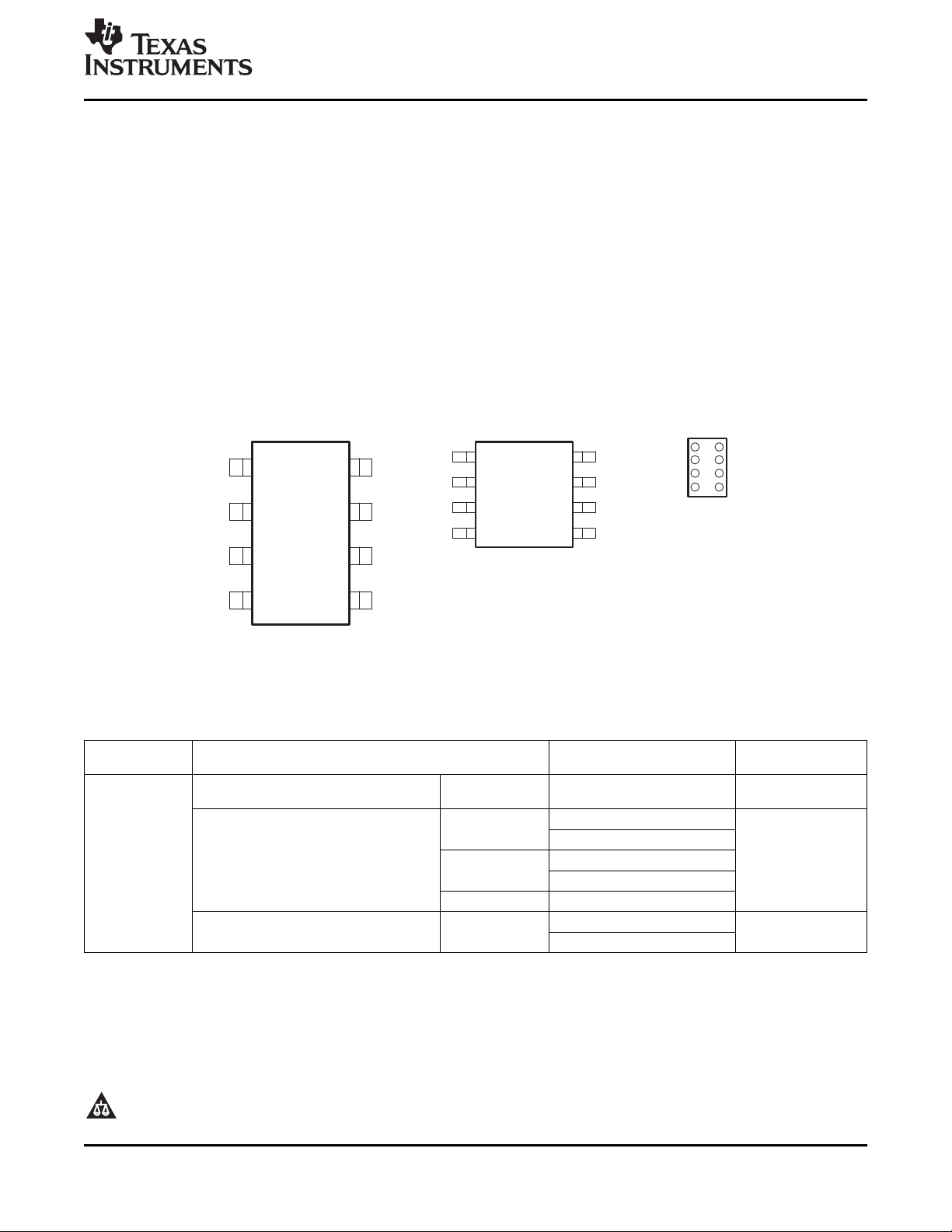
DGKPACKAGE
(TOP VIEW)
GND
P3
5
4
SCLP2
3 6
P1
2
SDA
7
V
CC
8
1
P0
B2B1
C2C1
D2D1
A2A1
YZP PACKAGE
(BOTTOMVIEW)
Seemechanicaldrawingsfordimensions.
4
5
GND
P3
3
P2 SCL
6
2
SDAP1
7
1
P0
V
CC
8
DPACKAGE
(TOP VIEW)
REMOTE 4-BIT I2C AND SMBus I/O EXPANDER
www.ti.com
1
FEATURES
2
• Available in the Texas Instruments NanoFree™ • No Glitch on Power Up
Package
• Power-Up With All Channels Configured as
• Low Standby Current Consumption of Inputs
1 μ A Max
• I2C to Parallel Port Expander
• Noise Filter on SCL/SDA Inputs
• Latched Outputs With High-Current Drive
• Operating Power-Supply Voltage Range of Maximum Capability for Directly Driving LEDs
2.3 V to 5.5 V
• Latch-Up Performance Exceeds 100 mA Per
• 5-V Tolerant I/O Ports JESD 78, Class II
• 400-kHz Fast I2C Bus • ESD Protection Exceeds JESD 22
• Input/Output Configuration Register – 2000-V Human-Body Model (A114-A)
• Polarity Inversion Register – 200-V Machine Model (A115-A)
• Internal Power-On Reset – 1000-V Charged-Device Model (C101)
WITH CONFIGURATION REGISTERS
SCPS125E – APRIL 2006 – REVISED OCTOBER 2007
PCA9536
DESCRIPTION/ORDERING INFORMATION
T
A
– 40 ° C to 85 ° C
(1) Package drawings, thermal data, and symbolization are available at www.ti.com/packaging .
(2) For the most current package and ordering information, see the Package Option Addendum at the end of this document, or see the TI
website at www.ti.com .
(3) DGK: The actual top-side marking has one additional character that designates the wafer fab/assembly site.
1
2 NanoFree is a trademark of Texas Instruments.
PRODUCTION DATA information is current as of publication date.
Products conform to specifications per the terms of the Texas
Instruments standard warranty. Production processing does not
necessarily include testing of all parameters.
Please be aware that an important notice concerning availability, standard warranty, and use in critical applications of
Texas Instruments semiconductor products and disclaimers thereto appears at the end of this data sheet.
ORDERING INFORMATION
PACKAGE
NanoFree™ – WCSP (DSBGA)
0.23-mm Large Bump – YZP (Pb-free)
SOIC – D PCA9536D PD536
VSSOP – DGK Reel of 2500 7C_
(1) (2)
ORDERABLE PART NUMBER
Reel of 3000 PCA9536YZPR 7CH
Reel of 2500
Tube of 75
PCA9536DR
PCA9536DRG4
PCA9536DG4
Reel of 250 PCA9536DT
PCA9536DGKR
PCA9536DGKRG4
Copyright © 2006 – 2007, Texas Instruments Incorporated
TOP-SIDE
MARKING
(3)
www.ti.com
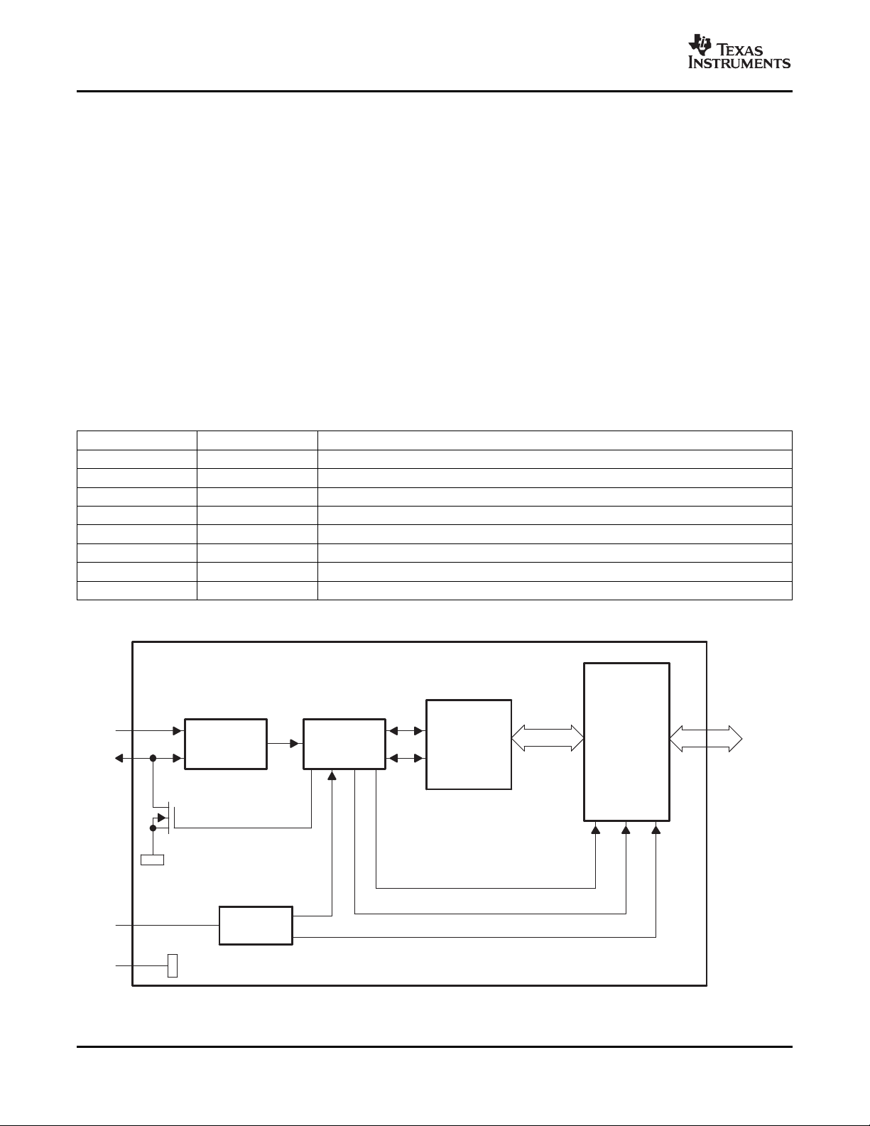
6
I/O
Port
Shift
Register
4 Bits
Input
Filter
7
Power-On
Reset
Read Pulse
Write Pulse
8
4
GND
V
CC
SDA
SCL
I2C Bus
Control
P3−P0
PCA9536
REMOTE 4-BIT I2C AND SMBus I/O EXPANDER
WITH CONFIGURATION REGISTERS
SCPS125E – APRIL 2006 – REVISED OCTOBER 2007
DESCRIPTION/ORDERING INFORMATION (CONTINUED)
This 4-bit I/O expander for the two-line bidirectional bus (I2C) is designed for 2.3-V to 5.5-V V
provides general-purpose remote I/O expansion for most microcontroller families via the I2C interface [serial clock
(SCL), serial data (SDA)].
The PCA9536 features 4-bit Configuration (input or output selection), Input Port, Output Port, and Polarity
Inversion (active high or active low) registers. At power on, the I/Os are configured as inputs with a weak pullup
to V
. However, the system master can enable the I/Os as either inputs or outputs by writing to the I/O
CC
configuration bits. If no signals are applied externally to the PCA9536, the voltage level is 1, or high, because of
the internal pullup resistors. The data for each input or output is stored in the corresponding Input Port or Output
Port register. The polarity of the Input Port register can be inverted with the Polarity Inversion register. All
registers can be read by the system master.
The system master can reset the PCA9536 in the event of a timeout or other improper operation by utilizing the
power-on reset feature, which puts the registers in their default state and initializes the I2C/SMBus state machine.
The device's outputs (latched) have high-current drive capability for directly driving LEDs. It has low current
consumption.
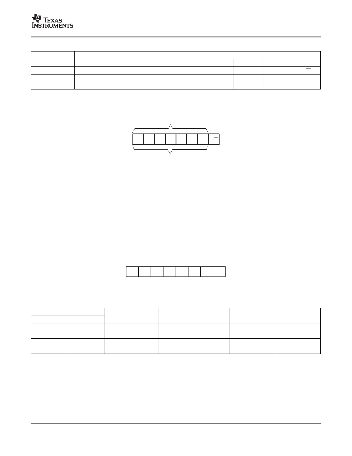
TERMINAL FUNCTIONS
NO. NAME DESCRIPTION
1 P0 P-port input/output. Push-pull design structure.
2 P1 P-port input/output. Push-pull design structure.
3 P2 P-port input/output. Push-pull design structure.
4 GND Ground
5 P3 P-port input/output. Push-pull design structure.
6 SCL Serial clock bus. Connect to V
7 SDA Serial data bus. Connect to V
8 V
CC
Supply voltage
CC
through a pullup resistor.
CC
through a pullup resistor.
operation. It
CC
LOGIC DIAGRAM
A. All I/Os are set to inputs at reset.
2 Submit Documentation Feedback Copyright © 2006 – 2007, Texas Instruments Incorporated
Product Folder Link(s): PCA9536
www.ti.com
Data From
Shift Register
Data From
Shift Register
Write Configuration
Pulse
Write Pulse
Read Pulse
Write Polarity
Pulse
Data From
Shift Register
Output Port
Register
Configuration
Register
Input Port
Register
Polarity
Inversion
Register
Polarity
Register Data
Input Port
Register Data
GND
ESD Protection
Diode
P0 to P3
V
CC
Output Port
Register Data
Q1
Q2
D
C
K
FF
Q
Q
D
C
K
FF
Q
Q
D
C
K
FF
Q
Q
D
C
K
FF
Q
Q
100 kW
REMOTE 4-BIT I2C AND SMBus I/O EXPANDER
WITH CONFIGURATION REGISTERS
SIMPLIFIED SCHEMATIC OF P0 TO P3
PCA9536
SCPS125E – APRIL 2006 – REVISED OCTOBER 2007
I/O Port
When an I/O is configured as an input, FETs Q1 and Q2 are off, creating a high-impedance input with a weak
pullup (100 k Ω typ) to V
If the I/O is configured as an output, Q1 or Q2 is enabled, depending on the state of the output port register. In
this case, there are low-impedance paths between the I/O pin and either V
applied to this I/O pin should not exceed the recommended levels for proper operation.
I2C Interface
The bidirectional I2C bus consists of the serial clock (SCL) and serial data (SDA) lines. Both lines must be
connected to a positive supply through a pullup resistor when connected to the output stages of a device. Data
transfer may be initiated only when the bus is not busy.
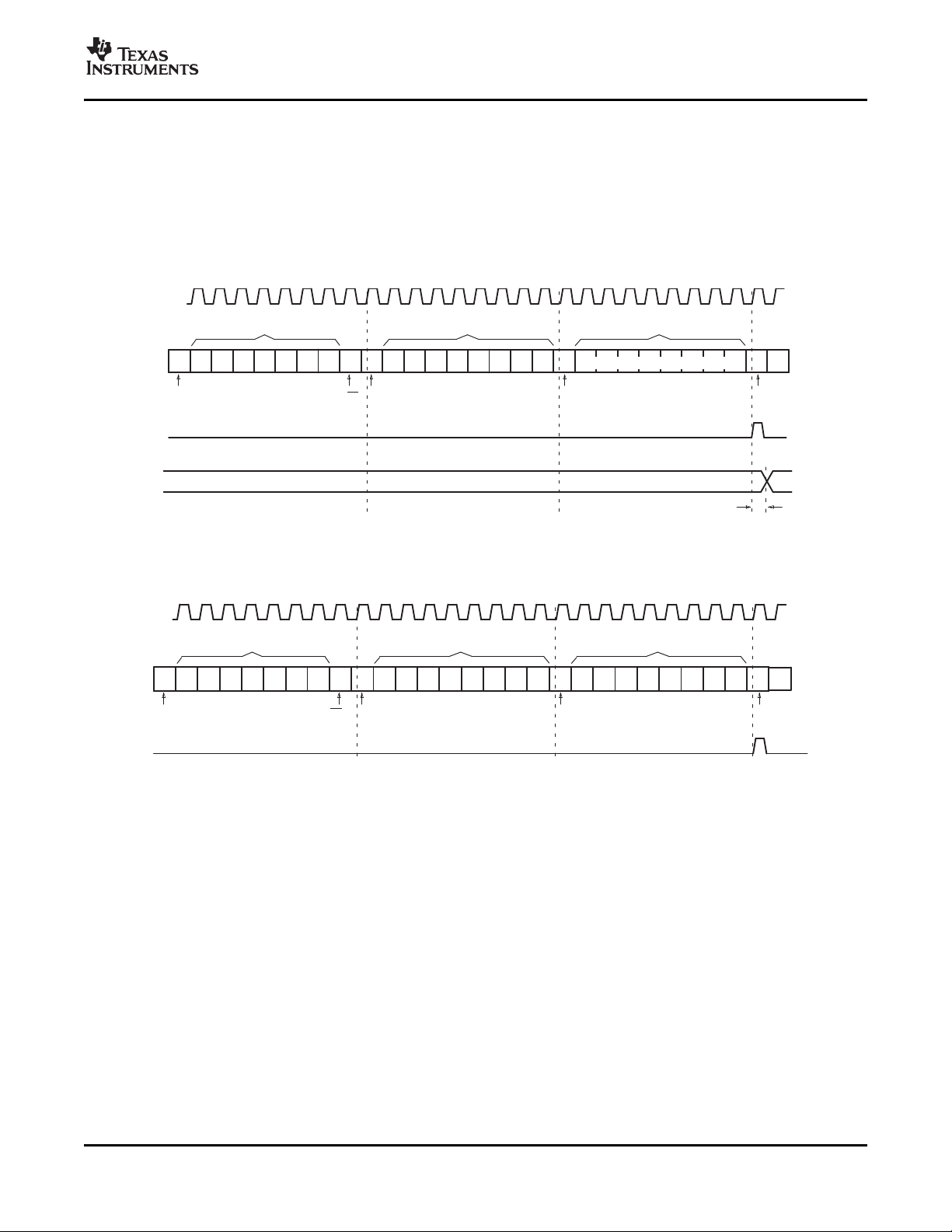
I2C communication with this device is initiated by a master sending a Start condition, a high-to-low transition on
the SDA input/output while the SCL input is high (see Figure 1 ). After the Start condition, the device address byte
is sent, most-significant bit (MSB) first, including the data direction bit (R/ W).
After receiving the valid address byte, this device responds with an acknowledge (ACK), a low on the SDA
input/output during the high of the ACK-related clock pulse.
On the I2C bus, only one data bit is transferred during each clock pulse. The data on the SDA line must remain
stable during the high pulse of the clock period, as changes in the data line at this time are interpreted as control
commands (Start or Stop) (see Figure 2 ).
A Stop condition, a low-to-high transition on the SDA input/output while the SCL input is high, is sent by the
master (see Figure 1 ).
A. At power-on reset, all registers return to default values.
. The input voltage may be raised above V
CC
to a maximum of 5.5 V.
CC
or GND. The external voltage
CC
Copyright © 2006 – 2007, Texas Instruments Incorporated Submit Documentation Feedback 3
Product Folder Link(s): PCA9536
www.ti.com
SDA
SCL
Start Condition
S
Stop Condition
P
SDA
SCL
Data Line
Stable;
Data Valid
Change
of Data
Allowed
Data Output
by Transmitter
SCL From
Master
Start
Condition
S
1 2 8 9
Data Output
by Receiver
Clock Pulse for
Acknowledgment
NACK
ACK
PCA9536
REMOTE 4-BIT I2C AND SMBus I/O EXPANDER
WITH CONFIGURATION REGISTERS
SCPS125E – APRIL 2006 – REVISED OCTOBER 2007
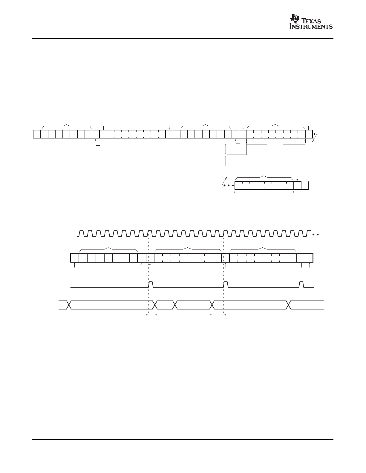
Any number of data bytes can be transferred from the transmitter to receiver between the Start and the Stop
conditions. Each byte of eight bits is followed by one ACK bit. The transmitter must release the SDA line before
the receiver can send an ACK bit. The device that acknowledges must pull down the SDA line during the ACK
clock pulse, so that the SDA line is stable low during the high pulse of the ACK-related clock period (see
Figure 3 ). When a slave receiver is addressed, it must generate an ACK after each byte is received. Similarly,
the master must generate an ACK after each byte that it receives from the slave transmitter. Setup and hold
times must be met to ensure proper operation.
A master receiver signals an end of data to the slave transmitter by not generating an acknowledge (NACK) after
the last byte has been clocked out of the slave. This is done by the master receiver by holding the SDA line high.
In this event, the transmitter must release the data line to enable the master to generate a Stop condition.
Figure 1. Definition of Start and Stop Conditions
Figure 2. Bit Transfer
Figure 3. Acknowledgment on the I2C Bus
4 Submit Documentation Feedback Copyright © 2006 – 2007, Texas Instruments Incorporated
Product Folder Link(s): PCA9536
www.ti.com
1 0
Slave Address
R/W
Fixed
10000
0 0 0 0 B1 B000
PCA9536
REMOTE 4-BIT I2C AND SMBus I/O EXPANDER
WITH CONFIGURATION REGISTERS
SCPS125E – APRIL 2006 – REVISED OCTOBER 2007
Interface Definition
BYTE
I2C slave address H L L L L L H R/ W
Px I/O data bus P3 P2 P1 P0
7 (MSB) 6 5 4 3 2 1 0 (LSB)
Does not affect operation of the PCA9536
P7 P6 P5 P4
Device Address
Figure 4 shows the address byte of the PCA9536.
Figure 4. PCA9536 Address
BIT
The slave address equates to 65 (decimal) and 41 (hexadecimal).
The last bit of the slave address defines the operation (read or write) to be performed. When it is high (1), a read
is selected, while a low (0) selects a write operation.
Control Register and Command Byte
Following the successful acknowledgment of the address byte, the bus master sends a command byte that is
stored in the control register in the PCA9536. Two bits of this data byte state the operation (read or write) and
the internal register (Input, Output, Polarity Inversion, or Configuration) that will be affected. This register can be
written or read through the I2C bus. The command byte is sent only during a write transmission.
Once a command byte has been sent, the register that was addressed continues to be accessed by reads until a
new command byte has been sent.
Figure 5. Control Register Bits
Command Byte
CONTROL REGISTER BITS
B1 B0
0 0 0x00 Input Port Read byte 1111 XXXX
0 1 0x01 Output Port Read/write byte 1111 1111
1 0 0x02 Polarity Inversion Read/write byte 0000 0000
1 1 0x03 Configuration Read/write byte 1111 1111
COMMAND BYTE POWER-UP
(HEX) DEFAULT
REGISTER PROTOCOL
Copyright © 2006 – 2007, Texas Instruments Incorporated Submit Documentation Feedback 5
Product Folder Link(s): PCA9536
www.ti.com
PCA9536
REMOTE 4-BIT I2C AND SMBus I/O EXPANDER
WITH CONFIGURATION REGISTERS
SCPS125E – APRIL 2006 – REVISED OCTOBER 2007
Register Descriptions
The Input Port register (register 0) reflects the incoming logic levels of the pins, regardless of whether the pin is
defined as an input or an output by the Configuration register. It only acts on read operation. Writes to these
registers have no effect. The default value, X, is determined by the externally applied logic level.
Before a read operation, a write transmission is sent with the command byte to instruct the I2C device that the
Input Port register will be accessed next.
Register 0 (Input Port Register)
BIT I3 I2 I1 I0
DEFAULT 1 1 1 1 X X X X
The Output Port register (register 1) shows the outgoing logic levels of the pins defined as outputs by the
Configuration register. Bit values in this register have no effect on pins defined as inputs. In turn, reads from this
register reflect the value that is in the flip-flop controlling the output selection, not the actual pin value.
BIT O3 O2 O1 O0
DEFAULT 1 1 1 1 1 1 1 1
I7 I6 I5 I4
Not Used
Register 1 (Output Port Register)
O7 O6 O5 O4
Not Used
The Polarity Inversion register (register 2) allows polarity inversion of pins defined as inputs by the Configuration
register. If a bit in this register is set (written with 1), the corresponding port pin's polarity is inverted. If a bit in this
register is cleared (written with a 0), the corresponding port pin's original polarity is retained.
Register 2 (Polarity Inversion Register)
BIT N3 N2 N1 N0
DEFAULT 0 0 0 0 0 0 0 0
N7 N6 N5 N4
Not Used
The Configuration register (register 3) configures the directions of the I/O pins. If a bit in this register is set to 1,
the corresponding port pin is enabled as an input with high-impedance output driver. If a bit in this register is
cleared to 0, the corresponding port pin is enabled as an output.
Register 3 (Configuration Register)
BIT C3 C2 C1 C0
DEFAULT 1 1 1 1 1 1 1 1
C7 C6 C5 C4
Not Used
Power-On Reset
When power (from 0 V) is applied to V
V
has reached V
CC
. At that time, the reset condition is released and the PCA9536 registers and I2C/SMBus
POR
state machine initialize to their default states. After that, V
the operating voltage for a power-reset cycle.
, an internal power-on reset holds the PCA9536 in a reset condition until
CC
must be lowered to below 0.2 V and then back up to
CC
6 Submit Documentation Feedback Copyright © 2006 – 2007, Texas Instruments Incorporated
Product Folder Link(s): PCA9536
www.ti.com
SCL
Start Condition
Data 1 Valid
SDA
Write to Port
Data Out
From Port
R/W ACK From Slave
ACK From Slave
ACK From Slave
1 98765432
Data 1101 0S 00 0 1 0 A 0000000 A A P
t
pv
Data to PortCommand ByteSlave Address
Data101 0S 00 0 1 0 A 1000000 A A P
SCL
SDA
Data to
Register
Start Condition R/W ACK From Slave ACK From Slave ACK From Slave
1 98765432
Data to RegisterCommand ByteSlave Address
PCA9536
REMOTE 4-BIT I2C AND SMBus I/O EXPANDER
WITH CONFIGURATION REGISTERS
SCPS125E – APRIL 2006 – REVISED OCTOBER 2007
Bus Transactions
Data is exchanged between the master and PCA9536 through write and read commands.
Writes
Data is transmitted to the PCA9536 by sending the device address and setting the least-significant bit (LSB) to a
logic 0 (see Figure 4 for device address). The command byte is sent after the address and determines which
register receives the data that follows the command byte. There is no limitation on the number of data bytes sent
in one write transmission (see Figure 6 and Figure 7 ).
Figure 6. Write to Output Port Register
<br/>
Figure 7. Write to Configuration or Polarity Inversion Registers
Copyright © 2006 – 2007, Texas Instruments Incorporated Submit Documentation Feedback 7
Product Folder Link(s): PCA9536
www.ti.com
01 0S 00 0 1 0 A A
Data from Register
Slave Address
Slave Address
R/W
ACK From
Slave
Command Byte
ACK From
Slave
S 01 0 00 0 1
R/W
1 A Data
A
ACK From
Master
Data
Data from Register
NACK From Master
NA
P
Last Byte
ACK From
Slave
At this time, the master-transmitter
becomes master-receiver and
slave-receiver becomes
slave-transmitter
SCL
SDA
Start
Condition
R/W
Read From
Port
Data Into
Port
Stop
Condition
ACK From
Master
NACK From
Master
ACK From
Slave
Data From Port
Slave Address Data From Port
1 98765432
01 0S 00 0 1 0 A
Data 1 Data 4
A NA
P
Data 2 Data 3 Data 4
t
ph
t
ps
Data 5
PCA9536
REMOTE 4-BIT I2C AND SMBus I/O EXPANDER
WITH CONFIGURATION REGISTERS
SCPS125E – APRIL 2006 – REVISED OCTOBER 2007
Reads
The bus master first must send the PCA9536 address with the LSB set to a logic 0 (see Figure 4 for device
address). The command byte is sent after the address and determines which register is accessed. After a restart,
the device address is sent again but, this time, the LSB is set to a logic 1. Data from the register defined by the
command byte then is sent by the PCA9536 (see Figure 8 and Figure 9 ). After a restart, the value of the register
defined by the command byte matches the register being accessed when the restart occurred. Data is clocked
into the register on the rising edge of the ACK clock pulse. There is no limitation on the number of data bytes
received in one read transmission, but when the final byte is received, the bus master must not acknowledge the
data.
Figure 8. Read From Register
<br/>
A. This figure assumes that the command byte previously has been programmed with 00h.
B. Transfer of data can be stopped at any moment by a Stop condition.
C. This figure eliminates the command byte transfer, a restart, and the slave address call between the initial slave
address call and actual data transfer from the P-port (see Figure 8 ).
Figure 9. Read Input Port Register
8 Submit Documentation Feedback Copyright © 2006 – 2007, Texas Instruments Incorporated
Product Folder Link(s): PCA9536
www.ti.com
REMOTE 4-BIT I2C AND SMBus I/O EXPANDER
WITH CONFIGURATION REGISTERS
SCPS125E – APRIL 2006 – REVISED OCTOBER 2007
PCA9536
Absolute Maximum Ratings
(1)
over operating free-air temperature range (unless otherwise noted)
MIN MAX UNIT
V
CC
V
I
V
O
I
IK
I
OK
I
IOK
I
OL
I
OH
I
CC
θ
JA
T
stg
(1) Stresses beyond those listed under "absolute maximum ratings" may cause permanent damage to the device. These are stress ratings
(2) The input negative-voltage and output voltage ratings may be exceeded if the input and output current ratings are observed.
(3) The package thermal impedance is calculated in accordance with JESD 51-7.
Supply voltage range – 0.5 6 V
Input voltage range
Output voltage range
(2)
(2)
– 0.5 6 V
– 0.5 6 V
Input clamp current VI< 0 – 20 mA
Output clamp current VO< 0 – 20 mA
Input/output clamp current VO< 0 or VO> V
Continuous output low current VO= 0 to V
Continuous output high current VO= 0 to V
CC
CC
CC
Continuous current through GND – 200
Continuous current through V
CC
D package 97
Package thermal impedance
(3)
DGK package 172 ° C/W
YZP package 102
Storage temperature range – 65 150 ° C
only, and functional operation of the device at these or any other conditions beyond those indicated under "recommended operating
conditions" is not implied. Exposure to absolute-maximum-rated conditions for extended periods may affect device reliability.
± 20 mA
50 mA
– 50 mA
160
mA
Recommended Operating Conditions
V
CC
V
IH
V
IL
I
OH
I
OL
T
A
Supply voltage 2.3 5.5 V
High-level input voltage V
Low-level input voltage V
High-level output current P3 – P0 – 10 mA
Low-level output current P3 – P0 25 mA
Operating free-air temperature – 40 85 ° C
MIN MAX UNIT
SCL, SDA 0.7 × V
CC
P3 – P0 2 5.5
SCL, SDA – 0.5 0.3 × V
P3 – P0 – 0.5 0.8
5.5
CC
Copyright © 2006 – 2007, Texas Instruments Incorporated Submit Documentation Feedback 9
Product Folder Link(s): PCA9536

www.ti.com
PCA9536
REMOTE 4-BIT I2C AND SMBus I/O EXPANDER
WITH CONFIGURATION REGISTERS
SCPS125E – APRIL 2006 – REVISED OCTOBER 2007
Electrical Characteristics
over recommended operating free-air temperature range (unless otherwise noted)
PARAMETER TEST CONDITIONS V
V
V
Input diode clamp voltage II= – 18 mA 2.3 V to 5.5 V – 1.2 V
IK
Power-on reset voltage VI= V
POR
or GND, IO= 0 V
CC
CC
POR
MIN TYP
2.3 V 1.8
IOH= – 8 mA
V
P-port high-level
OH
output voltage
(2)
IOH= – 10 mA
3 V 2.6
4.5 V 4.1
4.75 V 4.1
2.3 V 1.7
3 V 2.5
4.5 V 4
4.75 V 4
SDA V
= 0.4 V 2.3 V to 5.5 V 3 10
OL
2.3 V 8 10
V
= 0.5 V
OL
I
OL
(3)
P-port
V
= 0.7 V
OL
3 V 8 14
4.5 V 8 17
4.75 V 8 32 mA
2.3 V 10 13
3 V 10 19
4.5 V 10 24
4.75 V 10 44
I
I
I
SCL, SDA VI= V
I
P-port VI= V
IH
P-port VI= GND 2.3 V to 5.5 V – 100 μ A
IL
or GND 2.3 V to 5.5 V ± 1 μ A
CC
CC
2.3 V to 5.5 V 1 μ A
5.5 V 73 150
VI= V
I/O = inputs, f
Operating mode
VI= V
I/O = inputs, f
I
CC
VI= GND, IO= 0,
I/O = inputs, f
Standby mode
VI= V
I/O = inputs, f
One input at V
Δ I
Additional current in
CC
standby mode
Other inputs at V
Every LED I/O at VI= 4.3 V,
f
C
C
SCL VI= V
i
SDA 5 6.5
io
P-port 7.5 9.5
VIO= V
, IO= 0,
CC
= 400 kHz
scl
3.6 V 9 50
2.7 V 7 30
5.5 V 14 25
, IO= 0,
CC
= 100 kHz
scl
3.6 V 9 20
2.7 V 6 15
5.5 V 225 350
= 0 kHz
scl
3.6 V 175 250
2.7 V 125 200
5.5 V 0.25 1
, IO= 0,
CC
= 0 kHz
scl
CC
CC
= 0 kHz
scl
– 0.6 V,
CC
or GND
CC
or GND 2.3 V to 5.5 V 4 5 pF
or GND 2.3 V to 5.5 V pF
3.6 V 0.2 0.9
2.7 V 0.1 0.8
2.3 V to 5.5 V 0.35
5.5 V 0.4
(1) All typical values are at nominal supply voltage (2.5-V, 3.3-V, or 5-V VCC) and TA= 25 ° C.
(2) The total current sourced by all I/Os must be limited to 85 mA.
(3) Each I/O must be limited externally to a maximum of 25 mA, and the P-port (P3 – P0) must be limited to a maximum current of 100 mA.
(1)
MAX UNIT
1.5 1.65 V
V
μ A
mA
10 Submit Documentation Feedback Copyright © 2006 – 2007, Texas Instruments Incorporated
Product Folder Link(s): PCA9536

www.ti.com
REMOTE 4-BIT I2C AND SMBus I/O EXPANDER
WITH CONFIGURATION REGISTERS
SCPS125E – APRIL 2006 – REVISED OCTOBER 2007
I2C Interface Timing Requirements
over recommended operating free-air temperature range (unless otherwise noted) (see Figure 10 )
STANDARD MODE FAST MODE
I2C BUS I2C BUS
MIN MAX MIN MAX
f
t
t
t
t
t
t
t
t
t
t
t
t
t
t
C
(1) Cb= Total capacitive load of one bus in pF
I2C clock frequency 0 100 0 400 kHz
scl
I2C clock high time 4 0.6 μ s
sch
I2C clock low time 4.7 1.3 μ s
scl
I2C spike time 50 50 ns
sp
I2C serial-data setup time 250 100 ns
sds
I2C serial-data hold time 0 0 ns
sdh
I2C input rise time 1000 20 + 0.1C
icr
I2C input fall time 300 20 + 0.1C
icf
I2C output fall time, 10-pF to 400-pF bus 300 20 + 0.1C
ocf
I2C bus free time between Stop and Start 4.7 1.3 μ s
buf
I2C Start or repeated Start condition setup time 4.7 0.6 μ s
sts
I2C Start or repeated Start condition hold time 4 0.6 μ s
sth
I2C Stop condition setup time 4 0.6 μ s
sps
Valid data time, SCL low to SDA output valid 1 0.9 μ s
vd(data)
Valid data time of ACK condition, ACK signal from SCL low to SDA (out)
vd(ack)
low
I2C bus capacitive load 400 400 pF
b
1 0.9 μ s
PCA9536
UNIT
(1)
b
(1)
b
(1)
b
300 ns
300 ns
300 ns
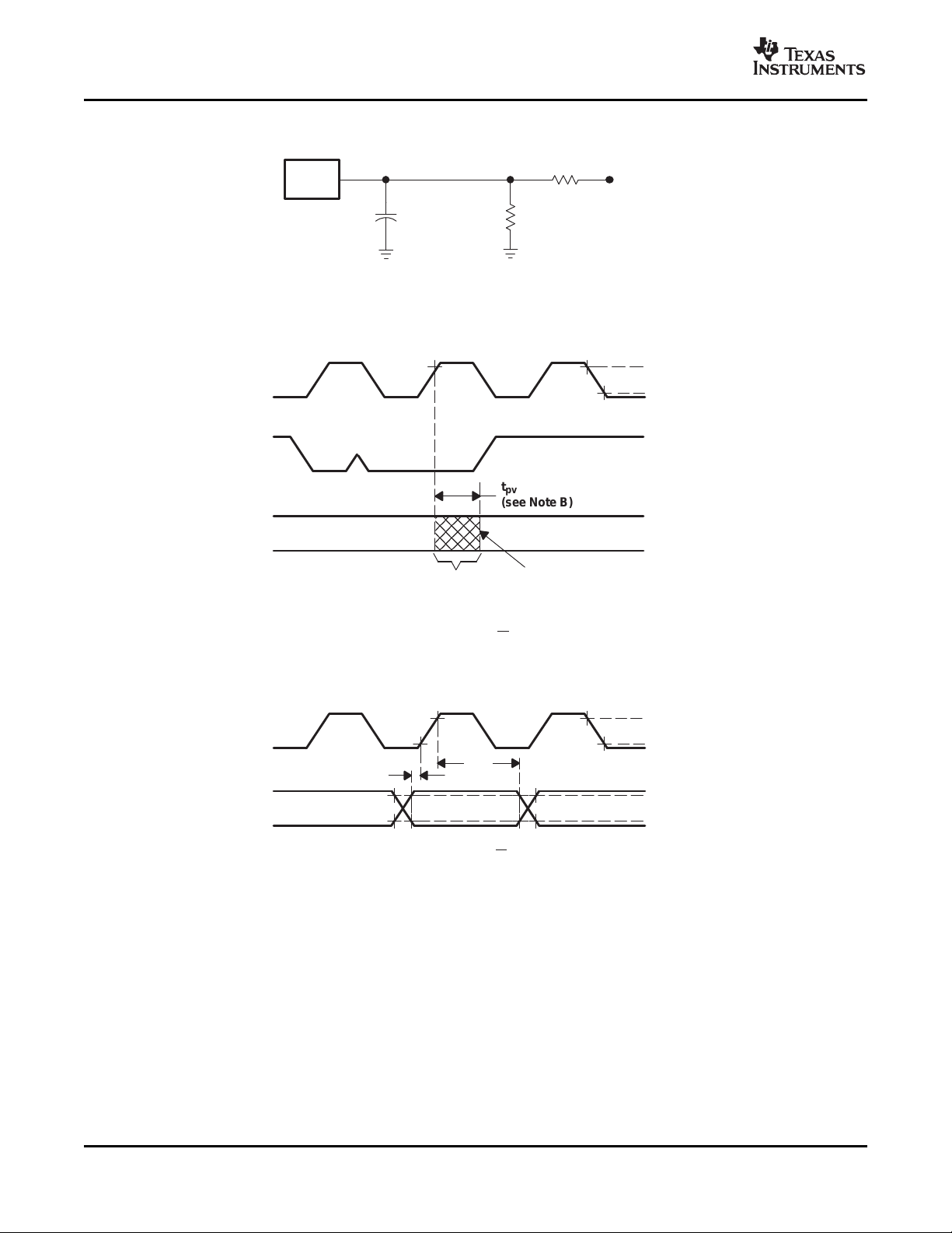
Switching Characteristics
over recommended operating free-air temperature range (unless otherwise noted) (see Figure 12 )
PARAMETER UNIT
t
Output data valid SCL P3 – P0 200 200 ns
pv
t
Input data setup time P-port SCL 100 100 ns
ps
t
Input data hold time P-port SCL 1 1 μ s
ph
FROM TO
(INPUT) (OUTPUT)
STANDARD MODE FAST MODE
I2C BUS I2C BUS
MIN MAX MIN MAX
Copyright © 2006 – 2007, Texas Instruments Incorporated Submit Documentation Feedback 11
Product Folder Link(s): PCA9536

www.ti.com
0
5
10
15
20
25
30
35
40
45
50
55
-50 -25 0 25 50 75 100
TA– Free-Air Temperature – °C
I
CC
– Supply Current – µA
VCC= 2.5 V
VCC= 3.3 V
VCC= 5 V
f
SCL
= 400 kHz
I/Os unloaded
0
50
100
150
200
250
300
-50 -25 0 25 50 75 100
TA– Free-Air Temperature – °C
I
CC
– Supply Current – nA
VCC= 2.5 V
VCC= 3.3 V
VCC= 5 V
SCL = V
CC
0
10
20
30
40
50
60
70
2.3 2.7 3.1 3.5 3.9 4.3 4.7 5.1 5.5
V
CC
– Supply Voltage – V
I
CC
– Supply Current – µA
f
SCL
= 400 kHz
I/Os unloaded
0
25
50
75
100
125
150
175
200
225
250
275
300
0 1 2 3 4
Number of I/Os Held L ow
I
CC
– Supply Current – µA
TA= –40°C
VCC= 5 V
TA= 25°C
TA= 85°C
0
25
50
75
100
125
150
175
200
225
250
275
300
-50 - 25 0 25 50 75 100
TA– Free-Air Temperature – °C
V
OL
– Outpu t Low Voltage – mV
VCC= 5 V, I
SINK
= 10 mA
VCC= 2.5 V, I
SINK
= 10 mA
VCC= 2.5 V, I
SINK
= 1 mA
VCC= 5 V, I
SINK
= 1 mA
0
25
50
75
100
125
150
175
200
225
250
275
300
-50 -25 0 25 50 75 100
TA– Free-Air Temperature – °C
(V
CC
– V
OH
) – Outp ut High Voltage – mV
VCC= 5 V, IOL= 10 mA
VCC= 2.5 V, IOL= 10 mA
0
5
10
15
20
25
30
0.0 0.1 0.2 0.3 0.4 0.5 0.6 0.7
VOL– Outpu t Low Voltage – V
ISINK – I/O Sink Current – mA
TA= –40°C
VCC= 2.5 V
TA= 25°C
TA= 85°C
0
5
10
15
20
25
30
35
40
45
50
55
60
0.0 0.1 0.2 0.3 0.4 0.5 0.6 0.7
VOL– Outpu t Low Voltage – V
ISINK – I/O Sink Current – mA
TA= –40°C
VCC= 5 V
TA= 25°C
TA= 85°C
0
5
10
15
20
25
30
35
40
0.0 0.1 0.2 0.3 0.4 0.5 0.6 0.7
VOL– Outpu t Low Voltage – V
ISINK – I/O Sink Current – mA
TA= –40°C
VCC= 3.3 V
TA= 25°C
TA= 85°C
PCA9536
REMOTE 4-BIT I2C AND SMBus I/O EXPANDER
WITH CONFIGURATION REGISTERS
SCPS125E – APRIL 2006 – REVISED OCTOBER 2007
TYPICAL CHARACTERISTICS
TA= 25 ° C (unless otherwise noted)
SUPPLY CURRENT QUIESCENT SUPPLY CURRENT SUPPLY CURRENT
vs vs vs
TEMPERATURE TEMPERATURE SUPPLY VOLTAGE
SUPPLY CURRENT I/O OUTPUT LOW VOLTAGE I/O OUTPUT HIGH VOLTAGE
vs vs vs
NUMBER OF I/Os HELD LOW TEMPERATURE TEMPERATURE
I/O SINK CURRENT I/O SINK CURRENT I/O SINK CURRENT
OUTPUT LOW VOLTAGE OUTPUT LOW VOLTAGE OUTPUT LOW VOLTAGE
12 Submit Documentation Feedback Copyright © 2006 – 2007, Texas Instruments Incorporated
vs vs vs
Product Folder Link(s): PCA9536

www.ti.com
0
5
10
15
20
25
30
0.0 0.1 0.2 0.3 0.4 0.5 0.6 0.7
(VCC– VOH) – Outp ut High Voltage – V
I
SOURCE
– I/O Source Current – mA
TA= –40°C
VCC= 2.5 V
TA= 25°C
TA= 85°C
0
5
10
15
20
25
30
35
40
45
50
55
60
65
70
0.0 0.1 0.2 0.3 0.4 0.5 0.6 0.7
(VCC– VOH) – Outp ut High Voltage – V
I
SOURCE
– I/O Source Current – mA
TA= –40°C
VCC= 5 V
TA= 25°C
TA= 85°C
0
5
10
15
20
25
30
35
40
45
0.0 0.1 0.2 0.3 0.4 0.5 0.6 0.7
(VCC– VOH) – Outp ut High Voltage – V
I
SOURCE
– I/O Source Current – mA
TA= –40°C
VCC= 3.3 V
TA= 25°C
TA= 85°C
0
1
2
3
4
5
6
2.3 2.7 3.1 3.5 3.9 4.3 4.7 5.1 5.5
VCC– Supply Voltage – V
V
OH
– Outpu t High Voltage – V
IOH= –10 mA
IOH= –8 mA
TA= 25°C
TA= 25 ° C (unless otherwise noted)
PCA9536
REMOTE 4-BIT I2C AND SMBus I/O EXPANDER
WITH CONFIGURATION REGISTERS
SCPS125E – APRIL 2006 – REVISED OCTOBER 2007
TYPICAL CHARACTERISTICS (continued)
I/O SOURCE CURRENT I/O SOURCE CURRENT I/O SOURCE CURRENT
vs vs vs
OUTPUT HIGH VOLTAGE OUTPUT HIGH VOLTAGE OUTPUT HIGH VOLTAGE
OUTPUT HIGH VOLTAGE
vs
SUPPLY VOLTAGE
Copyright © 2006 – 2007, Texas Instruments Incorporated Submit Documentation Feedback 13
Product Folder Link(s): PCA9536

www.ti.com
RL = 1 kΩ
V
CC
CL = 50 pF
(see Note A)
t
buf
t
icr
t
sth
t
sds
t
sdh
t
icf
t
icr
t
scl
t
sch
t
sts
t
PHL
t
PLH
0.3 × V
CC
Stop
Condition
t
sps
Repeat
Start
Condition
Start or
Repeat
Start
Condition
SCL
SDA
Start
Condition
(S)
Address
Bit 7
(MSB)
Data
Bit 0
(LSB)
Stop
Condition
(P)
Three Bytes for Complete
Device Programming
SDA LOAD CONFIGURATION
VOLTAGE WAVEFORMS
t
icf
Stop
Condition
(P)
t
sp
DUT
SDA
0.7 × V
CC
0.3 × V
CC
0.7 × V
CC
R/W
Bit 0
(LSB)
ACK
(A)
Data
Bit 7
(MSB)
Address
Bit 1
Address
Bit 6
BYTE DESCRIPTION
1 I2C address
2, 3 P-port data
PCA9536
REMOTE 4-BIT I2C AND SMBus I/O EXPANDER
WITH CONFIGURATION REGISTERS
SCPS125E – APRIL 2006 – REVISED OCTOBER 2007
PARAMETER MEASUREMENT INFORMATION
A. CLinclude probe and jig capacitance.
B. All inputs are supplied by generators having the following characteristics: PRR ≤ 10 MHz, ZO= 50 Ω , tr/tf≤ 30 ns.
C. All parameters and waveforms are not applicable to all devices.
Figure 10. I2C Interface Load Circuit and Voltage Waveforms
14 Submit Documentation Feedback Copyright © 2006 – 2007, Texas Instruments Incorporated
Product Folder Link(s): PCA9536

www.ti.com
A
A
A
A
S 1 0 0 0 00 1 1 Data 1 1 PData 2
Start
Condition
8 Bits
(One Data Byte)
From Port
Data From PortSlave Address
R/W
87654321
t
ir
t
ir
t
sps
t
iv
Address Data 1 Data 2
INT
Data
Into
Port
B
B
A
A
P
n
INT
R/W A
t
ir
0.7 × V
CC
0.3 × V
CC
0.7 × V
CC
0.3 × V
CC
0.7 × V
CC
0.3 × V
CC
0.7 × V
CC
0.3 × V
CC
INT
SCL
View B−BView A−A
t
iv
RL = 4.7 kΩ
V
CC
CL = 100 pF
(see Note A)
INTERRUPT LOAD CONFIGURATION
DUT
INT
ACK
From Slave
ACK
From Slave
REMOTE 4-BIT I2C AND SMBus I/O EXPANDER
PARAMETER MEASUREMENT INFORMATION (continued)
PCA9536
WITH CONFIGURATION REGISTERS
SCPS125E – APRIL 2006 – REVISED OCTOBER 2007
A. CLinclude probe and jig capacitance.
B. All inputs are supplied by generators having the following characteristics: PRR ≤ 10 MHz, ZO= 50 Ω , tr/tf≤ 30 ns.
C. All parameters and waveforms are not applicable to all devices.
Figure 11. Interrupt Load Circuit and Voltage Waveforms
Copyright © 2006 – 2007, Texas Instruments Incorporated Submit Documentation Feedback 15
Product Folder Link(s): PCA9536
www.ti.com
P0 A
0.7 × V
CC
0.3 × V
CC
SCL
P3
t
pv
(see Note B)
Slave
ACK
Unstable
Data
Last Stable Bit
SDA
P
n
P
n
WRITE MODE (R/W = 0)
P0 A
0.7 × V
CC
0.3 × V
CC
SCL
P3
0.7 × V
CC
0.3 × V
CC
t
ps
t
ph
READ MODE (R/W = 1)
DUT
CL = 50 pF
(see Note A)
P-PORT LOAD CONFIGURATION
Pn
2 × V
CC
500 W
500 W
PCA9536
REMOTE 4-BIT I2C AND SMBus I/O EXPANDER
WITH CONFIGURATION REGISTERS
SCPS125E – APRIL 2006 – REVISED OCTOBER 2007
PARAMETER MEASUREMENT INFORMATION (continued)
A. CLinclude probe and jig capacitance.
B. tpvis measured from 0.7 × V
C. All inputs are supplied by generators having the following characteristics: PRR ≤ 10 MHz, ZO= 50 Ω , tr/tf≤ 30 ns.
D. The outputs are measured one at a time, with one transition per measurement.
E. All parameters and waveforms are not applicable to all devices.
CC
on SCL to 50% I/O (Pn) output.
Figure 12. P-Port Load Circuit and Voltage Waveforms
16 Submit Documentation Feedback Copyright © 2006 – 2007, Texas Instruments Incorporated
Product Folder Link(s): PCA9536

www.ti.com
SDA
SCL
Start
ACK or Read Cycle
t
w
t
REC
RESET
0.3 y V
CC
VCC/2
t
RESET
Px
(see Note D)
RL = 1 kΩ
V
CC
CL = 50 pF
(see Note A)
SDA LOAD CONFIGURATION
DUT
SDA
P-PORT LOAD CONFIGURATION
VCC/2
t
RESET
DUT
CL = 50 pF
(see Note A)
Pn
2 × V
CC
500 W
500 W
REMOTE 4-BIT I2C AND SMBus I/O EXPANDER
PARAMETER MEASUREMENT INFORMATION (continued)
PCA9536
WITH CONFIGURATION REGISTERS
SCPS125E – APRIL 2006 – REVISED OCTOBER 2007
Copyright © 2006 – 2007, Texas Instruments Incorporated Submit Documentation Feedback 17
A. CLinclude probe and jig capacitance.
B. All inputs are supplied by generators having the following characteristics: PRR ≤ 10 MHz, ZO= 50 Ω , tr/tf≤ 30 ns.
C. The outputs are measured one at a time, with one transition per measurement.
D. I/Os are configured as inputs.
E. All parameters and waveforms are not applicable to all devices.
Figure 13. Reset Load Circuits and Voltage Waveforms
Product Folder Link(s): PCA9536

www.ti.com
SDA
SCL
GND
P0
P1
P2
P3
GND
V
CC
V
CC
V
CC
10 kW 10 kW
2 kW
Master
Controller
PCA9536
INT
RESET
Subsystem 2
(e.g., counter)
Controlled Device
(e.g., CBT device)
ENABLE
A
B
Subsystem 1
(e.g., temperature
sensor)
SDA
SCL
PCA9536
REMOTE 4-BIT I2C AND SMBus I/O EXPANDER
WITH CONFIGURATION REGISTERS
SCPS125E – APRIL 2006 – REVISED OCTOBER 2007
APPLICATION INFORMATION
Figure 14 shows an application in which the PCA9536 can be used.
A. Device address is 10000001.
B. P0, P2, and P3 are configured as outputs.
C. P1 is configured as an input.
Figure 14. Typical Application
18 Submit Documentation Feedback Copyright © 2006 – 2007, Texas Instruments Incorporated
Product Folder Link(s): PCA9536
www.ti.com
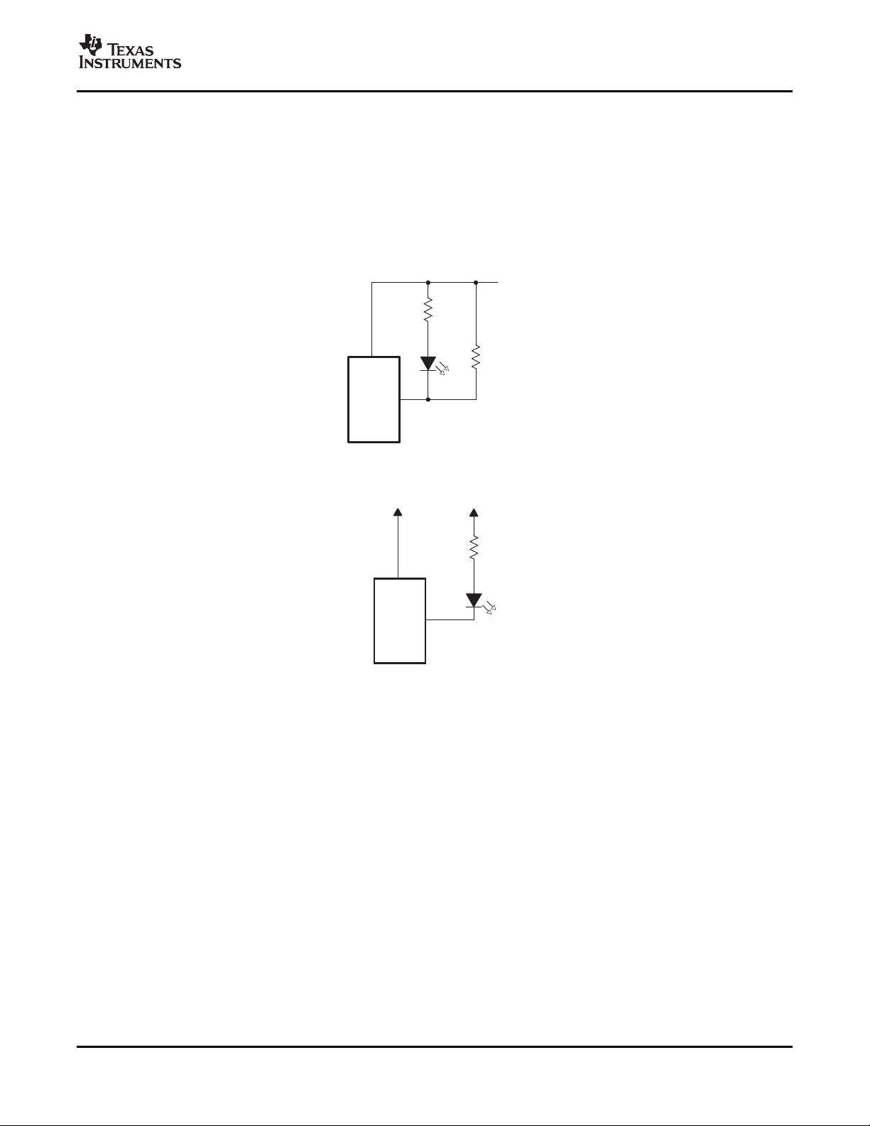
LED
Pn
V
CC
100 kW
V
CC
LED
3.3 V
5 V
Pn
V
CC
REMOTE 4-BIT I2C AND SMBus I/O EXPANDER
WITH CONFIGURATION REGISTERS
SCPS125E – APRIL 2006 – REVISED OCTOBER 2007
Minimizing ICCWhen I/Os Control LEDs
When the I/Os are used to control LEDs, they are normally connected to V
Figure 14 . The LED acts as a diode so, when the LED is off, the I/O V
current, ICC, increases as V
becomes lower than V
IN
and is specified as Δ ICCin Electrical Characteristics.
CC
is about 1.2 V less than V
IN
Designs needing to minimize current consumption, such as battery power applications, should consider
maintaining the I/O pins greater than or equal to V
in parallel with the LED. Figure 16 shows V
methods maintain the I/O V
at or above V
IN
CC
CC
when the LED is off. Figure 15 shows a high-value resistor
CC
less than the LED supply voltage by at least 1.2 V. Both of these
and prevent additional supply-current consumption when the LED
is off.
through a resistor as shown in
CC
PCA9536
. The supply
CC
Figure 15. High-Value Resistor in Parallel With the LED
Figure 16. Device Supplied by a Lower Voltage
Copyright © 2006 – 2007, Texas Instruments Incorporated Submit Documentation Feedback 19
Product Folder Link(s): PCA9536

PACKAGE OPTION ADDENDUM
www.ti.com
18-Jul-2007
PACKAGING INFORMATION
Orderable Device Status
(1)
Package
Type
Package
Drawing
Pins Package
Qty
Eco Plan
PCA9536D ACTIVE SOIC D 8 75 Green (RoHS &
no Sb/Br)
PCA9536DG4 ACTIVE SOIC D 8 75 Green (RoHS &
no Sb/Br)
PCA9536DGKR ACTIVE MSOP DGK 8 2500 Green (RoHS &
no Sb/Br)
PCA9536DGKRG4 ACTIVE MSOP DGK 8 2500 Green (RoHS &
no Sb/Br)
PCA9536DR ACTIVE SOIC D 8 2500 Green (RoHS &
no Sb/Br)
PCA9536DRG4 ACTIVE SOIC D 8 2500 Green (RoHS &
no Sb/Br)
(1)
The marketing status values are defined as follows:
ACTIVE: Product device recommended for new designs.
LIFEBUY: TI has announced that the device will be discontinued, and a lifetime-buy period is in effect.
NRND: Not recommended for new designs. Device is in production to support existing customers, but TI does not recommend using this part in
a new design.
PREVIEW: Device has been announced but is not in production. Samples may or may not be available.
OBSOLETE: TI has discontinued the production of the device.
(2)
Lead/Ball Finish MSL Peak Temp
CU NIPDAU Level-1-260C-UNLIM
CU NIPDAU Level-1-260C-UNLIM
CU NIPDAU Level-1-260C-UNLIM
CU NIPDAU Level-1-260C-UNLIM
CU NIPDAU Level-1-260C-UNLIM
CU NIPDAU Level-1-260C-UNLIM
(3)
(2)
Eco Plan - The planned eco-friendly classification: Pb-Free (RoHS), Pb-Free (RoHS Exempt), or Green (RoHS & no Sb/Br) - please check
http://www.ti.com/productcontent for the latest availability information and additional product content details.
TBD: The Pb-Free/Green conversion plan has not been defined.
Pb-Free (RoHS): TI's terms "Lead-Free" or "Pb-Free" mean semiconductor products that are compatible with the current RoHS requirements
for all 6 substances, including the requirement that lead not exceed 0.1% by weight in homogeneous materials. Where designed to be soldered
at high temperatures, TI Pb-Free products are suitable for use in specified lead-free processes.
Pb-Free (RoHS Exempt): This component has a RoHS exemption for either 1) lead-based flip-chip solder bumps used between the die and
package, or 2) lead-based die adhesive used between the die and leadframe. The component is otherwise considered Pb-Free (RoHS
compatible) as defined above.
Green (RoHS & no Sb/Br): TI defines "Green" to mean Pb-Free (RoHS compatible), and free of Bromine (Br) and Antimony (Sb) based flame
retardants (Br or Sb do not exceed 0.1% by weight in homogeneous material)
(3)
MSL, Peak Temp. -- The Moisture Sensitivity Level rating according to the JEDEC industry standard classifications, and peak solder
temperature.
Important Information and Disclaimer:The information provided on this page represents TI's knowledge and belief as of the date that it is
provided. TI bases its knowledge and belief on information provided by third parties, and makes no representation or warranty as to the
accuracy of such information. Efforts are underway to better integrate information from third parties. TI has taken and continues to take
reasonable steps to provide representative and accurate information but may not have conducted destructive testing or chemical analysis on
incoming materials and chemicals. TI and TI suppliers consider certain information to be proprietary, and thus CAS numbers and other limited
information may not be available for release.
In no event shall TI's liability arising out of such information exceed the total purchase price of the TI part(s) at issue in this document sold by TI
to Customer on an annual basis.
Addendum-Page 1

PACKAGE MATERIALS INFORMATION
www.ti.com
TAPE AND REEL INFORMATION
19-Mar-2008
*All dimensions are nominal
Device Package
Type
PCA9536DGKR MSOP DGK 8 2500 330.0 13.0 5.3 3.4 1.4 8.0 12.0 Q1
PCA9536DR SOIC D 8 2500 330.0 12.4 6.4 5.2 2.1 8.0 12.0 Q1
PCA9536DR SOIC D 8 2500 330.0 12.4 6.4 5.2 2.1 8.0 12.0 Q1
Package
Drawing
Pins SPQ Reel
Diameter
(mm)
Reel
Width
W1 (mm)
A0 (mm) B0 (mm) K0 (mm) P1
(mm)W(mm)
Pin1
Quadrant
Pack Materials-Page 1

PACKAGE MATERIALS INFORMATION
www.ti.com
19-Mar-2008
*All dimensions are nominal
Device Package Type Package Drawing Pins SPQ Length (mm) Width (mm) Height (mm)
PCA9536DGKR MSOP DGK 8 2500 358.0 335.0 35.0
PCA9536DR SOIC D 8 2500 346.0 346.0 29.0
PCA9536DR SOIC D 8 2500 340.5 338.1 20.6
Pack Materials-Page 2


IMPORTANT NOTICE
Texas Instruments Incorporated and its subsidiaries (TI) reserve the right to make corrections, modifications, enhancements, improvements,
and other changes to its products and services at any time and to discontinue any product or service without notice. Customers should
obtain the latest relevant information before placing orders and should verify that such information is current and complete. All products are
sold subject to TI’s terms and conditions of sale supplied at the time of order acknowledgment.
TI warrants performance of its hardware products to the specifications applicable at the time of sale in accordance with TI’s standard
warranty. Testing and other quality control techniques are used to the extent TI deems necessary to support this warranty. Except where
mandated by government requirements, testing of all parameters of each product is not necessarily performed.
TI assumes no liability for applications assistance or customer product design. Customers are responsible for their products and
applications using TI components. To minimize the risks associated with customer products and applications, customers should provide
adequate design and operating safeguards.
TI does not warrant or represent that any license, either express or implied, is granted under any TI patent right, copyright, mask work right,
or other TI intellectual property right relating to any combination, machine, or process in which TI products or services are used. Information
published by TI regarding third-party products or services does not constitute a license from TI to use such products or services or a
warranty or endorsement thereof. Use of such information may require a license from a third party under the patents or other intellectual
property of the third party, or a license from TI under the patents or other intellectual property of TI.
Reproduction of TI information in TI data books or data sheets is permissible only if reproduction is without alteration and is accompanied
by all associated warranties, conditions, limitations, and notices. Reproduction of this information with alteration is an unfair and deceptive
business practice. TI is not responsible or liable for such altered documentation. Information of third parties may be subject to additional
restrictions.
Resale of TI products or services with statements different from or beyond the parameters stated by TI for that product or service voids all
express and any implied warranties for the associated TI product or service and is an unfair and deceptive business practice. TI is not
responsible or liable for any such statements.
TI products are not authorized for use in safety-critical applications (such as life support) where a failure of the TI product would reasonably
be expected to cause severe personal injury or death, unless officers of the parties have executed an agreement specifically governing
such use. Buyers represent that they have all necessary expertise in the safety and regulatory ramifications of their applications, and
acknowledge and agree that they are solely responsible for all legal, regulatory and safety-related requirements concerning their products
and any use of TI products in such safety-critical applications, notwithstanding any applications-related information or support that may be
provided by TI. Further, Buyers must fully indemnify TI and its representatives against any damages arising out of the use of TI products in
such safety-critical applications.
TI products are neither designed nor intended for use in military/aerospace applications or environments unless the TI products are
specifically designated by TI as military-grade or "enhanced plastic." Only products designated by TI as military-grade meet military
specifications. Buyers acknowledge and agree that any such use of TI products which TI has not designated as military-grade is solely at
the Buyer's risk, and that they are solely responsible for compliance with all legal and regulatory requirements in connection with such use.
TI products are neither designed nor intended for use in automotive applications or environments unless the specific TI products are
designated by TI as compliant with ISO/TS 16949 requirements. Buyers acknowledge and agree that, if they use any non-designated
products in automotive applications, TI will not be responsible for any failure to meet such requirements.
Following are URLs where you can obtain information on other Texas Instruments products and application solutions:
Products Applications
Amplifiers amplifier.ti.com Audio www.ti.com/audio
Data Converters dataconverter.ti.com Automotive www.ti.com/automotive
DSP dsp.ti.com Broadband www.ti.com/broadband
Clocks and Timers www.ti.com/clocks Digital Control www.ti.com/digitalcontrol
Interface interface.ti.com Medical www.ti.com/medical
Logic logic.ti.com Military www.ti.com/military
Power Mgmt power.ti.com Optical Networking www.ti.com/opticalnetwork
Microcontrollers microcontroller.ti.com Security www.ti.com/security
RFID www.ti-rfid.com Telephony www.ti.com/telephony
RF/IF and ZigBee® Solutions www.ti.com/lprf Video & Imaging www.ti.com/video
Mailing Address: Texas Instruments, Post Office Box 655303, Dallas, Texas 75265
Copyright © 2008, Texas Instruments Incorporated
Wireless www.ti.com/wireless
 Loading...