

Page 1

OPA564
OPA564
www.ti.com
1.5A, 24V, 17MHz
POWER OPERATIONAL AMPLIFIER
Check for Samples: OPA564
1
FEATURES
23
• HIGH OUTPUT CURRENT: 1.5A
• WIDE POWER-SUPPLY RANGE:
– Single Supply: +7V to +24V
– Dual Supply: ±3.5V to ±12V
• LARGE OUTPUT SWING: 20VPPat 1.5A
• FULLY PROTECTED:
– THERMAL SHUTDOWN
– ADJUSTABLE CURRENT LIMIT
• DIAGNOSTIC FLAGS:
– OVER-CURRENT
– THERMAL SHUTDOWN
• OUTPUT ENABLE/SHUTDOWN CONTROL
• HIGH SPEED:
– GAIN-BANDWIDTH PRODUCT: 17MHz
– FULL-POWER BANDWIDTH AT 10VPP:
1.3MHz indicates current limit and the second shows a
– SLEW RATE: 40V/μs
• DIODE FOR JUNCTION TEMPERATURE
MONITORING
• HTSSOP-20, HSOP-20 PowerPAD™
PACKAGES
(Bottom- and Top-Side Thermal Pad Versions)
APPLICATIONS
• POWERLINE COMMUNICATIONS
• VALVE, ACTUATOR DRIVER
• V
• MOTOR DRIVER
• AUDIO POWER AMPLIFIER
• POWER-SUPPLY OUTPUT AMPLIFIER
• TEST EQUIPMENT AMPLIFIER
• TRANSDUCER EXCITATION
• LASER DIODE DRIVER
• GENERAL-PURPOSE LINEAR POWER
DRIVER
COM
BOOSTER
SBOS372C –OCTOBER 2008–REVISED NOVEMBER 2009
DESCRIPTION
The OPA564 is a low-cost, high-current operational
amplifier that is ideal for driving up to 1.5A into
reactive loads. The high slew rate provides 1.3MHz
full-power bandwidth and excellent linearity. These
monolithic integrated circuits provide high reliability in
demanding powerline communications and motor
control applications.
The OPA564 operates from a single supply of 7V to
24V, or dual power supplies of ±3.5V to ±12V. In
single-supply operation, the input common-mode
range extends to the negative supply. At maximum
output current, a wide output swing provides a 20V
(I
= 1.5A) capability with a nominal 24V supply.
OUT
The OPA564 is internally protected against
over-temperature conditions and current overloads. It
is designed to provide an accurate, user-selected
current limit. Two flag outputs are provided; one
thermal over-temperature condition. It also has an
Enable/Shutdown pin that can be forced low to shut
down the output, effectively disconnecting the load.
The OPA564 is housed in a thermally-enhanced,
surface-mount PowerPAD™ package (HSOP-20) with
the choice of the thermal pad on either the top side or
the bottom side of the package, and in an
HTSSOP-20 package with thermal pad on the
bottom. Operation for all versions is specified over
the industrial temperature range, –40°C to +85°C.
OPA564 RELATED PRODUCTS
FEATURES DEVICE
Zerø-Drift PGA with 2-Channel Input
Mux and SPI
Zerø-Drift Operational Amplifier,
50MHz, RRI/O, Single-Supply
Quad Operational Amplifier, JFET
Input , Low Noise
Power Operational Amplifier, 1.2A,
15V, 17MHz, 50V/μs
PGA112
OPA365
TL074
OPA561
PP
1
Please be aware that an important notice concerning availability, standard warranty, and use in critical applications of Texas
Instruments semiconductor products and disclaimers thereto appears at the end of this data sheet.
2PowerPAD is a trademark of Texas Instruments, Inc.
3All other trademarks are the property of their respective owners.
UNLESS OTHERWISE NOTED this document contains
PRODUCTION DATA information current as of publication date.
Products conform to specifications per the terms of Texas
Instruments standard warranty. Production processing does not
necessarily include testing of all parameters.
Copyright © 2008–2009, Texas Instruments Incorporated
Page 2
OPA564
SBOS372C –OCTOBER 2008–REVISED NOVEMBER 2009
www.ti.com
This integrated circuit can be damaged by ESD. Texas Instruments recommends that all integrated circuits be handled with
appropriate precautions. Failure to observe proper handling and installation procedures can cause damage.
ESD damage can range from subtle performance degradation to complete device failure. Precision integrated circuits may be more
susceptible to damage because very small parametric changes could cause the device not to meet its published specifications.
PACKAGE/ORDERING INFORMATION
(1)
PACKAGE
PRODUCT PACKAGE-LEAD DESIGNATOR PACKAGE MARKING
HSOP-20 (PowerPAD on bottom) DWP OPA564
OPA564 HSOP-20 (PowerPAD on top) DWD OPA564
HTSSOP-20 (PowerPAD on bottom)
(2)
PWP OPA564
(1) For the most current package and ordering information, see the Package Option Addendum at the end of this document, or see the TI
web site at www.ti.com.
(2) Product-preview device.
ABSOLUTE MAXIMUM RATINGS
(1)
Over operating free-air temperature range (unless otherwise noted)
OPA564 UNIT
Supply Voltage, VS= (V+) – (V–) +26 V
(2)
Signal Input
Terminals
Signal Output
Terminals
Output Short-Circuit
Operating Junction Temperature, T
Storage Temperature, T
Junction Temperature, T
Voltage
(2)
Current
Voltage (V–)–0.4 to (V+)+0.4 V
(3)
Current
(4)
J
A
J
Human Body Model (HBM) 4000 V
ESD Ratings Charged Device Model (CDM) 1000 V
Machine Model (MM) 200 V
(1) Stresses above these ratings may cause permanent damage. Exposure to absolute maximum conditions for extended periods may
degrade device reliability. These are stress ratings only, and functional operation of the device at these or any other conditions beyond
those specified is not supported.
(2) Input terminals are diode-clamped to the power-supply rails. Input signals that can swing more than 0.4V beyond the supply rails should
be current limited to 10mA or less.
(3) Output terminals are diode-clamped to the power-supply rails. Input signals forcing the output terminal more than 0.4V beyond the
supply rails should be current limited to 10mA or less.
(4) Short-circuit to ground within SOA. See Power Dissipation and Safe Operating Area for more information.
(V–)–0.4 to (V+)+0.4 V
±10 mA
±10 mA
Continuous
–40 to +125 °C
–55 to +150 °C
+150 °C
2 Submit Documentation Feedback Copyright © 2008–2009, Texas Instruments Incorporated
Product Folder Link(s): OPA564
Page 3
OPA564
www.ti.com
SBOS372C –OCTOBER 2008–REVISED NOVEMBER 2009
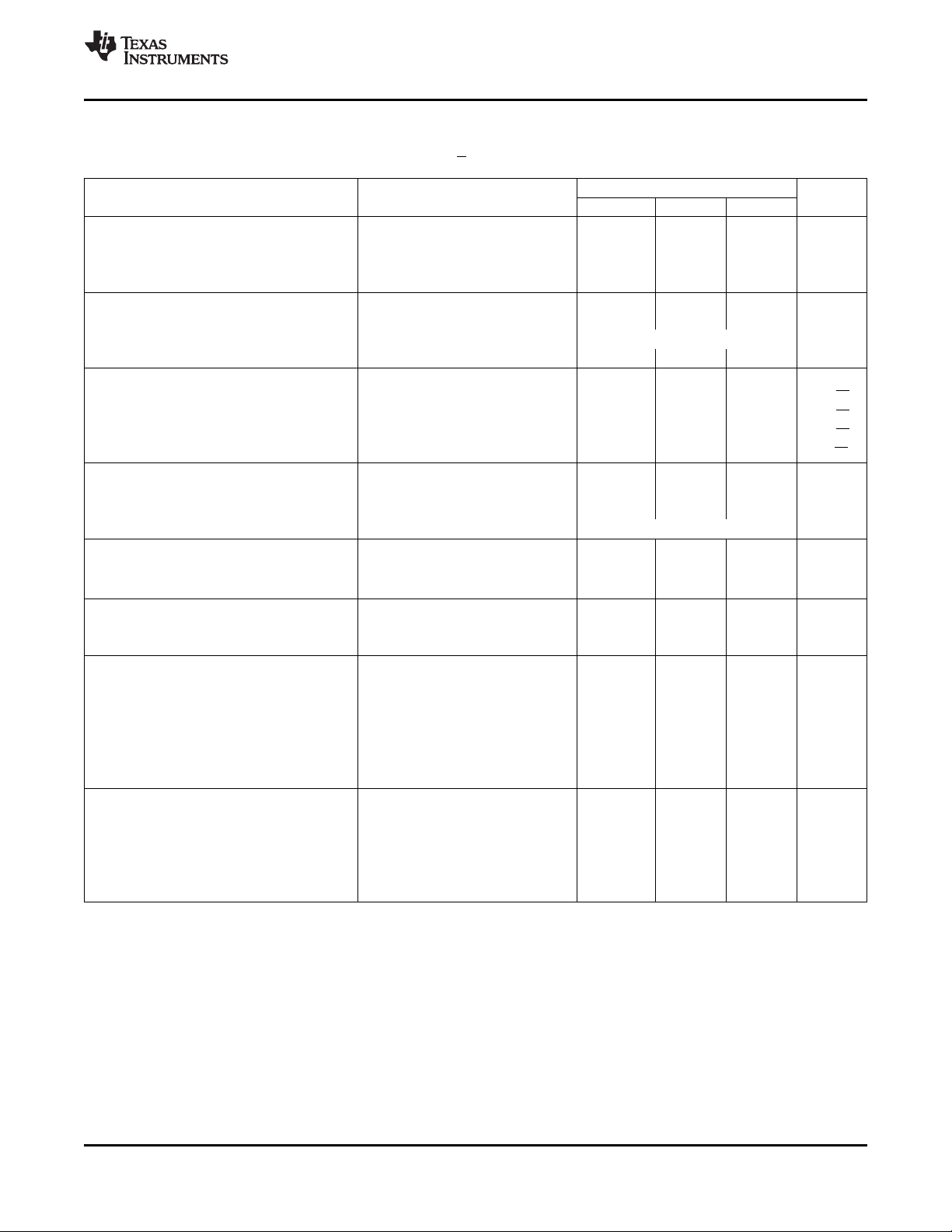
ELECTRICAL CHARACTERISTICS
Boldface limits apply over the specified temperature range: TA= –40°C to +85°C.
At T
OFFSET VOLTAGE
Input Offset Voltage V
INPUT BIAS CURRENT
Input Bias Current
Input Offset Current
NOISE
Input Voltage Noise Density e
Input Current Noise I
INPUT VOLTAGE RANGE
Common-Mode Voltage Range: V
Common-Mode Rejection Ratio CMRR VCM= (V–) to (V+)–3V 70 80 dB
INPUT IMPEDANCE
Differential Ω || pF
Common-Mode Ω || pF
OPEN-LOOP GAIN
Open-Loop Voltage Gain A
FREQUENCY RESPONSE
Gain-Bandwidth Product
Slew Rate SR G = 1, 10V Step 40 V/μs
Full Power Bandwidth G = +2, V
Settling Time ±0.1% G= +1, 10V Step, C
Total Harmonic Distortion + Noise THD+N f = 1kHz, R
OUTPUT
Voltage Output: V
(1) See Typical Characteristics.
= +25°C, VS= ±12V, R
CASE
= 20kΩ to GND, and E/S pin enabled, unless otherwise noted.
LOAD
OPA564
PARAMETERS CONDITIONS MIN TYP MAX UNIT
OS
VCM= 0V ±2 ±20 mV
vs Temperature dVOS/dT ±10 μV/°C
vs Power Supply PSRR VCM= 0V, VS= ±3.5V to ±13V 10 150 μV/V
(1)
I
B
VCM= 0V 10 100 pA
vs Temperature See Figure 10, Typical Characteristics
(1)
I
OS
n
f = 1kHz 102.8 nV/√Hz
10 100 pA
f = 10kHz 20 nV/√Hz
f = 100kHz 8 nV/√Hz
n
CM
f = 1kHz 4 fA/√Hz
Linear Operation (V–) (V+)–3 V
vs Temperature See Figure 9, Typical Characteristics
1012|| 16
1012|| 9
V
OL
(1)
GBW R
OUT
V
OUT
= 20VPP, R
= 20VPP, R
LOAD
±0.01% G = +1, 10V Step, C
= 5Ω, G = +1, V
LOAD
OUT
Positive I
Negative I
Positive I
Negative I
OUT
OUT
OUT
OUT
= 1kΩ 80 108 dB
LOAD
= 10Ω 93 dB
LOAD
= 5Ω 17 MHz
OUT
= 10V
PP
= 100pF 0.6 μs
LOAD
= 100pF 0.8 μs
LOAD
= 5V
OUT
P
1.3 MHz
0.003 %
= 0.5A (V+)–1 (V+)–0.4 V
= –0.5A (V–)+1 (V–)+0.3 V
= 1.5A (V+)–2 (V+)–1.5 V
= –1.5A (V–)+2 (V–)+1.1 V
Copyright © 2008–2009, Texas Instruments Incorporated Submit Documentation Feedback 3
Product Folder Link(s): OPA564
Page 4
OPA564
SBOS372C –OCTOBER 2008–REVISED NOVEMBER 2009
www.ti.com
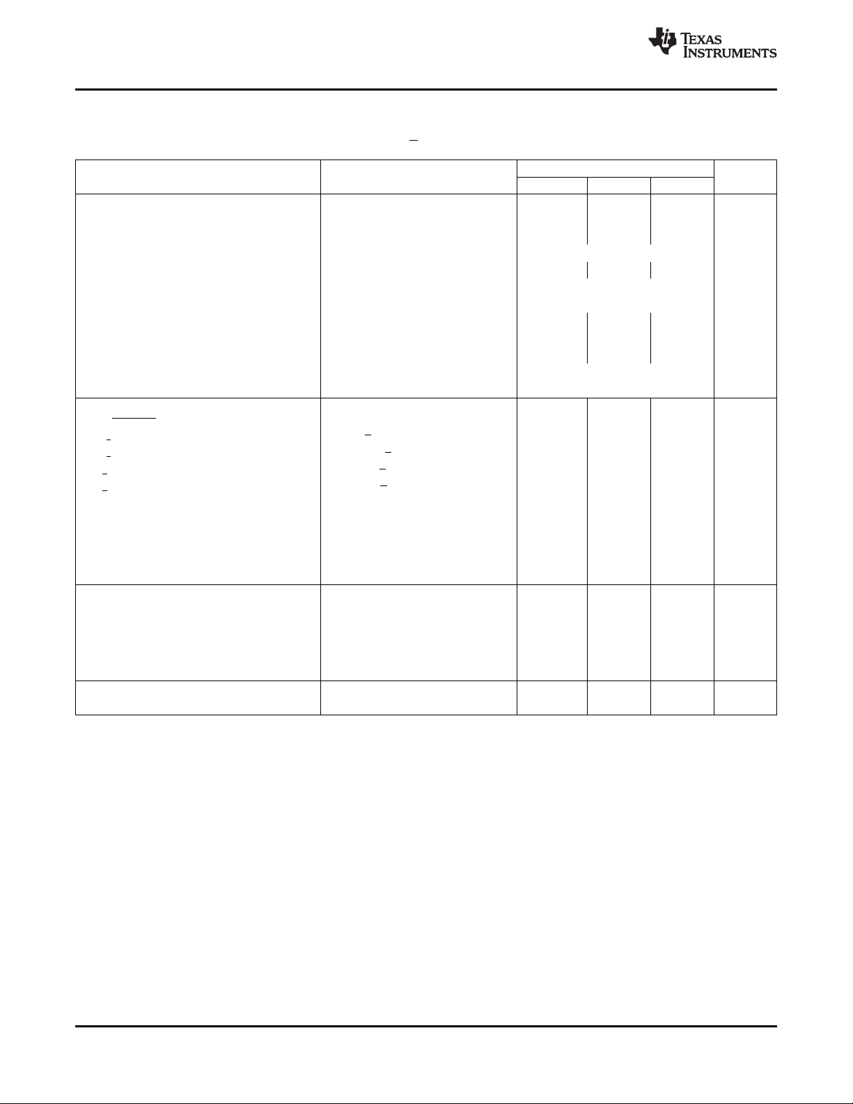
ELECTRICAL CHARACTERISTICS (continued)
Boldface limits apply over the specified temperature range: TA= –40°C to +85°C.
At T
OUTPUT, continued
Maximum Continuous Current, dc I
Output Impedance, closed loop R
Output Impedance, open loop Z
Output Current Limit Range
Current Limit Equation I
Current Limit Accuracy I
Current Limit Overshoot
Output Shut Down
Capacitive Load Drive C
DIGITAL CONTROL
Enable/Shutdown Mode INPUT V
Output Shutdown Time 1 μs
Output Enable Time 3 μs
Current Limit Flag Output
Thermal Shutdown
Junction Temperature at Shutdown
T
(2) Under safe operating conditions. See Power Dissipation and Safe Operating Area for safe operating area (SOA) information.
(3) Minimum current limit is 0.4A. See Adjustable Current Limit in the Applications section.
(4) Quiescent current increases when the current limit is increased (see Typical Characteristics).
(5) RCL(current limit) can range from 55kΩ (I
(6) See Typical Characteristics.
(7) Transient load transition time must be ≥ 200ns.
(8) See Enable/Shutdown (E/S) Pin in the Applications section.
(9) When sourcing, the V
(10) Characterized, but not production tested.
= +25°C, VS= ±12V, R
CASE
= 20kΩ to GND, and E/S pin enabled, unless otherwise noted.
LOAD
OPA564
PARAMETERS CONDITIONS MIN TYP MAX UNIT
(2)
OUT
O
O
(3)
LIM
f = 100kHz 10 Ω
G = +2, f = 100kHz See Figure 24, Typical Characteristics
I
@ 20k • (1.2V/RCL+ 5kΩ)
LIM
Solved for RCL(Current Limit) RCL@ (24k/I
= 1.5A 10 %
(6) (7)
Output Impedance
V
High (output enabled) E/S Pin Open or Forced High (V–)+2 (V–)+V
E/S
V
Low (output shut down) E/S Pin Forced Low (V–) (V–)+0.8 V
E/S
I
High (output enabled) E/S Pin Indicates High 10 μA
E/S
I
Low (output shut down) E/S Pin Indicates Low 1 μA
E/S
(8)
LOAD
VIN= 5V Pulse (200ns tr), G = +2 50 %
= +3.3V to +5.5V referenced to V–
DIG
LIM
See Figure 6, Typical Characteristics
1.5
±0.4 to ±2.0 A
(4) (5)
) – 5kΩ Ω
LIM
6 || 120 GΩ || pF
DIG
Normal Operation Sinking 10μA 0 (V–)+0.8 V
Current-Limited Sourcing 20μA (V–)+2 V
DIG
Normal Operation Sinking 200μA 0 (V–)+0.8 V
Thermally Shutdown
Hysteresis
SENSE
(10)
(9)
(10)
Sourcing 200μA (V–)+2 V
+140 to
DIG
+157
15 to 19 °C
Diode Ideality Factor η 1.085
= 400mA) to 7.5kΩ (I
OUT
supply must be able to supply the current.
DIG
= 1.5A). See Adjustable Current Limit in the Applications section.
OUT
A
A
V
V
V
°C
4 Submit Documentation Feedback Copyright © 2008–2009, Texas Instruments Incorporated
Product Folder Link(s): OPA564
Page 5
OPA564
www.ti.com
SBOS372C –OCTOBER 2008–REVISED NOVEMBER 2009
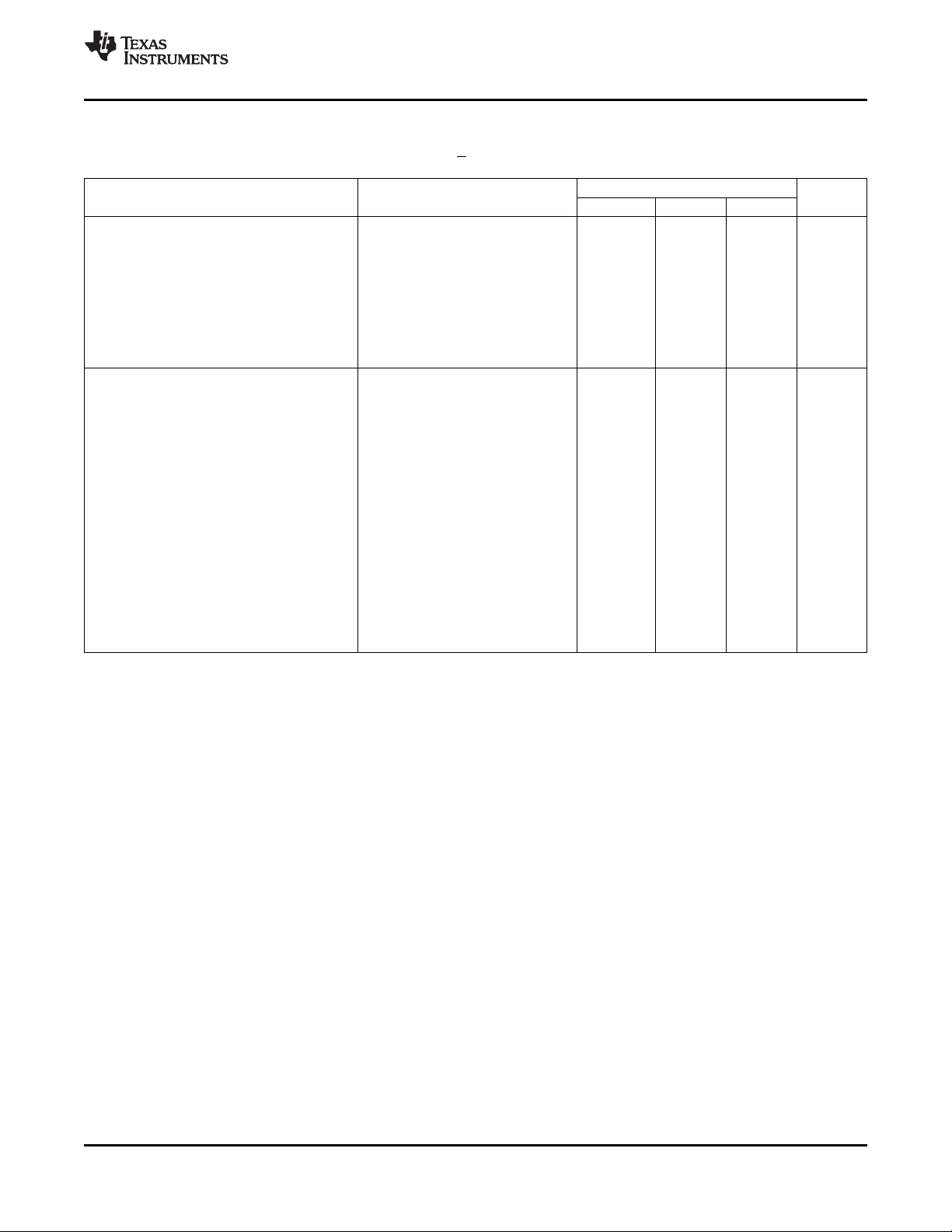
ELECTRICAL CHARACTERISTICS (continued)
Boldface limits apply over the specified temperature range: TA= –40°C to +85°C.
At T
POWER SUPPLY
Specified Voltage Range V
Operating Voltage Range 7 24 V
Quiescent Current
Quiescent Current in Shutdown Mode I
Specified Voltage for Digital V
Digital Quiescent Current I
TEMPERATURE RANGE
Specified Range –40 +85 °C
Operating Range –40 +125
Thermal Resistance
(11) Power-supply sequencing requirements must be observed. See Power Supplies section for more information.
(12) Quiescent current increases when the current limit is increased (see Typical Characteristics).
(13) I
(14) The OPA564 typically goes into thermal shutdown at a junction temperature above +140°C.
(15) Thermal modeling of the DWD-20 package was done based on a 1-inch AAVID Thermalloy heatsink (Thermalloy part no. 65810).
= +25°C, VS= ±12V, R
CASE
= 20kΩ to GND, and E/S pin enabled, unless otherwise noted.
LOAD
OPA564
PARAMETERS CONDITIONS MIN TYP MAX UNIT
(11)
±12 V
(12)
S
I
I
Q
Connected to V–
SET
(13)
, I
= 0 39 50 mA
OUT
Over Temperature 50 mA
I
QSD
DIG
DIG
HSOP-20 DWP PowerPAD (Pad Down) θ
HSOP-20 DWD PowerPAD (Pad Up)
(15)
HTSSOP-20 PWP PowerPAD θ
should not be connected to V– because this consumes excessive current. A 7.5kΩ resistor connected in series sets I
SET
maximum output current.
JA
θ
JC
θ
JP
θ
JB
θ
JA
θ
JC
θ
JB
JA
θ
JC
θ
JP
θ
JB
Connected to V–
SET
V
DIG
High K Board 33 °C/W
High K Board 45.5 °C/W
High K Board 42.4 °C/W
(13)
5 mA
(V–) + 3.3 (V–) + 5.5 V
= 5V 43 100 μA
(14)
50 °C/W
1.83 °C/W
22 °C/W
6.3 °C/W
22 °C/W
43.6 °C/W
6.26 °C/W
20.9 °C/W
to the
LIM
°C
Copyright © 2008–2009, Texas Instruments Incorporated Submit Documentation Feedback 5
Product Folder Link(s): OPA564
Page 6
1
2
3
4
5
6
7
8
9
10
20
19
18
17
16
15
14
13
12
11
V-
V+PWR
V+PWR
V+PWR
V
OUT
V
OUT
V PWR-
V PWR-
T
SENSE
V-
V-
V+
T
FLAG
E/S
+IN
-IN
V
DIG
I
FLAG
I
SET
V-
PowerPAD
HeatSink
(Locatedon
topside)
(2)
(2)PowerPADisinternallyconnectedtoV .-
1
2
3
4
5
6
7
8
9
10
20
19
18
17
16
15
14
13
12
11
V-
V+
T
FLAG
E/S
+IN
-IN
V
DIG
I
FLAG
I
SET
V-
V-
V+PWR
V+PWR
V+PWR
V
OUT
V
OUT
V PWR-
V PWR-
T
SENSE
V-
PowerPAD
HeatSink
(Locatedon
bottomside)
(1)
(1)PowerPADisinternallyconnectedtoV ,
Soldering the PowerPAD to the PCB is
always required, even with applications that
havelowpowerdissipation.
-
OPA564
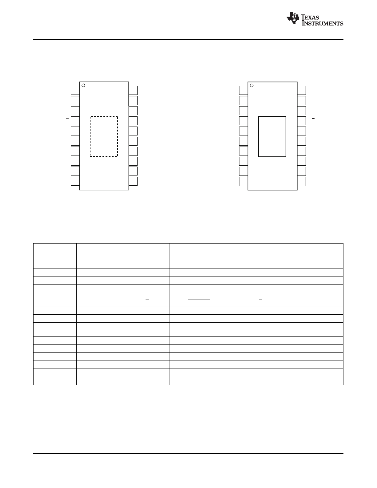
SBOS372C –OCTOBER 2008–REVISED NOVEMBER 2009
OPA564AIDWP, OPA564AIPWP OPA564AIDWD
HSOP-20, HTSSOP-20 HSOP-20
PowerPAD on Bottom PowerPAD on Top
www.ti.com
PIN CONFIGURATIONS
PIN DESCRIPTIONS
OPA564AIDWP
OPA564AIPWP OPA564AIDWD
(PAD DOWN) (PAD UP)
PIN NO. PIN NO. NAME DESCRIPTION
1, 10, 11, 20 1, 10, 11, 20 V– –Supply for Amplifier, PWR Out, and Metal PowerPAD
2 19 V+ +Supply for Signal Amplifier
3 18 T
4 17 E/S Enable/Shutdown Output Stage; take E/S low to shut down output
5 16 +IN Noninverting Op Amp Input
6 15 –IN Inverting Op Amp Input
7 14 V
8 13 I
9 12 I
6 Submit Documentation Feedback Copyright © 2008–2009, Texas Instruments Incorporated
12 9 T
13, 14 7, 8 V– PWR –Supply for Power Output Stage
15, 16 5, 6 V
17, 18, 19 3, 4, 2 V+ PWR +Supply for Power Output Stage
FLAG
DIG
FLAG
SET
SENSE
OUT
Thermal Over Temperature Flag; flag is high when alarmed and device has
gone into thermal shutdown.
+Supply for Digital Flag and E/S (referenced to V–).
Valid Range is (V–) + 3.3V ≤ V
Current Limit Flag; Active High
Current Limit Set (see Applications Section)
Temperature Sense Pin for use with TMP411
Output Voltage; ROis high impedance when shut down
Product Folder Link(s): OPA564
≤ (V–) + 5.5V.
DIG
Page 7
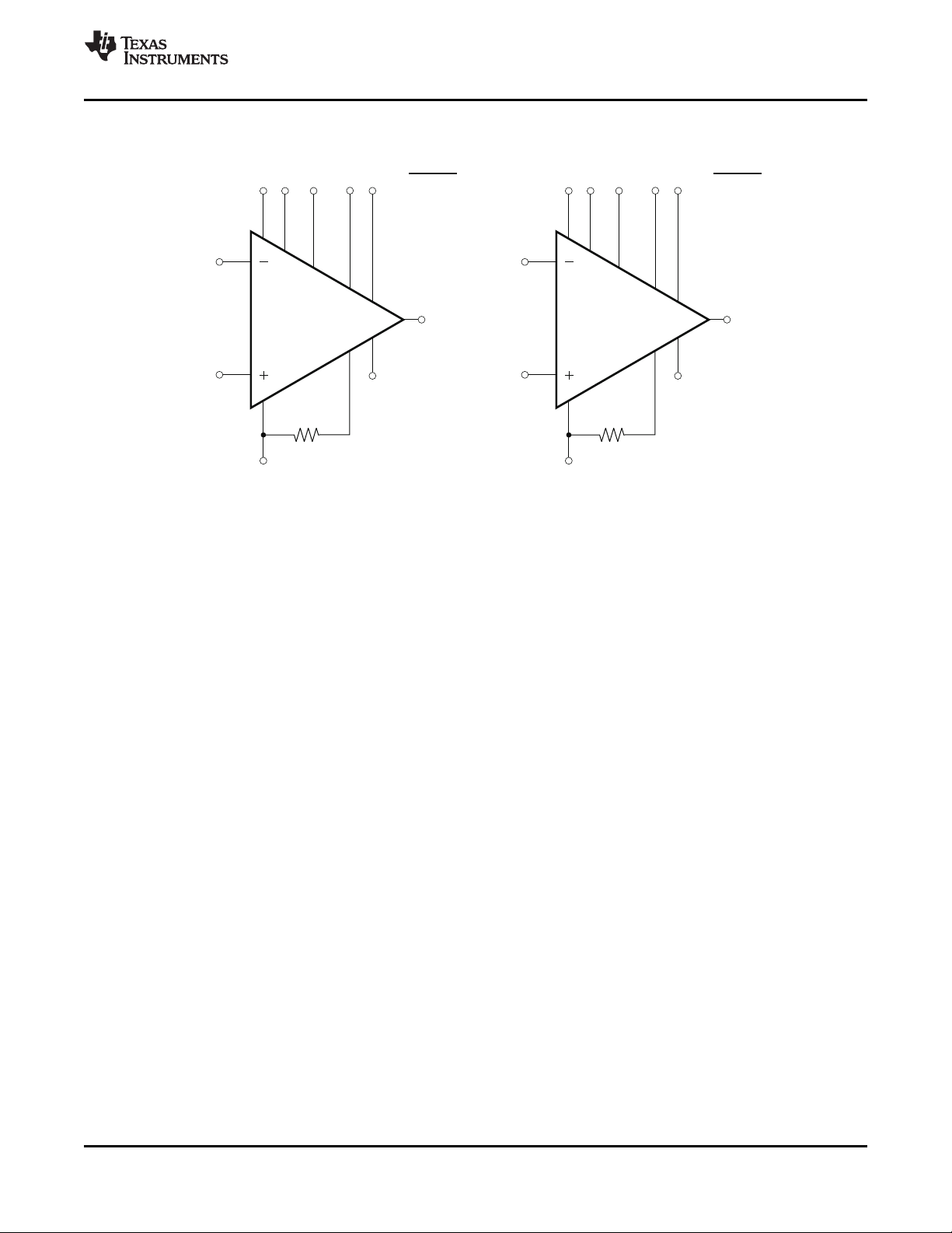
Enable/Shutdown
V-
Current
Limit
Flag
Thermal
Flag
V
DIG
V+
Enable/Shutdown
Current
Limit
Flag
Thermal
Flag
V
DIG
V+
-IN
+IN
OPA564AIDWP
OPA564AIPWP
OPA564AIDWD
Current
Limit
Set
R
CL
T
SENSE
V
OUT
(2)
(19)
(17,18)
(6)
(5)
(1,10,11,20)
(13,14)
(7)
(3)
(8)
(4)
(12)
(9)
(15,16)
V-
-IN
+IN
Current
Limit
Set
R
CL
T
SENSE
V
OUT
(19)
(2)
(3,4)
(15)
(16)
(1,10,11,20)
(7,8)
(14)
(18)
(13)
(17)
(9)
(12)
(5,6)
OPA564
www.ti.com
SBOS372C –OCTOBER 2008–REVISED NOVEMBER 2009
FUNCTIONAL PIN DIAGRAM
Copyright © 2008–2009, Texas Instruments Incorporated Submit Documentation Feedback 7
Product Folder Link(s): OPA564
Page 8
14
12
10
8
6
4
2
0
-2
-4
-6
-8
-10
-12
-14
0 0.2
OutputCurrent(A)
OutputVoltage(V)
1.60.4 0.6 0.8 1.0 1.2 1.4
V = 3.5VS±
V = 12VS±
+125 C°
+25 C°
- °40 C
R =7.5kCLW
1msCurrentPulses
V = 12VS±
40
38
36
34
32
30
28
26
24
22
20
QuiescentCurrent(mA)
6 10 20 24
SupplyVoltage(V)
8 12 14 16 18 22
R =7.5kCLW
R =40kCLW
R =100kCLW
2V/div
Time(250ns/div)
Input
Output
Unloaded
G=+1
V =9V
IN PP
2V/div
Time(250ns/div)
Input
Output
5 Load
G=+1
V =9V
W
IN PP
Time(250ns/div)
10mV/div
R =
C =0pF
LOAD
LOAD
NoLoad
G= 1
-
V
OUT
V
IN
60
50
40
30
20
10
0
Overshoot(%)
10 100
1k 10k 100k
Capacitance(pF)
V = 12VS±
G=+1
G=+10
G= 10-
G= 1-
OPA564
SBOS372C –OCTOBER 2008–REVISED NOVEMBER 2009
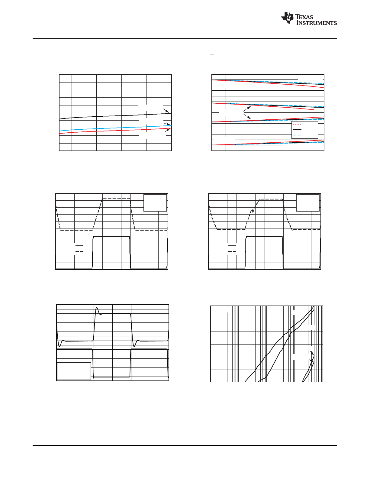
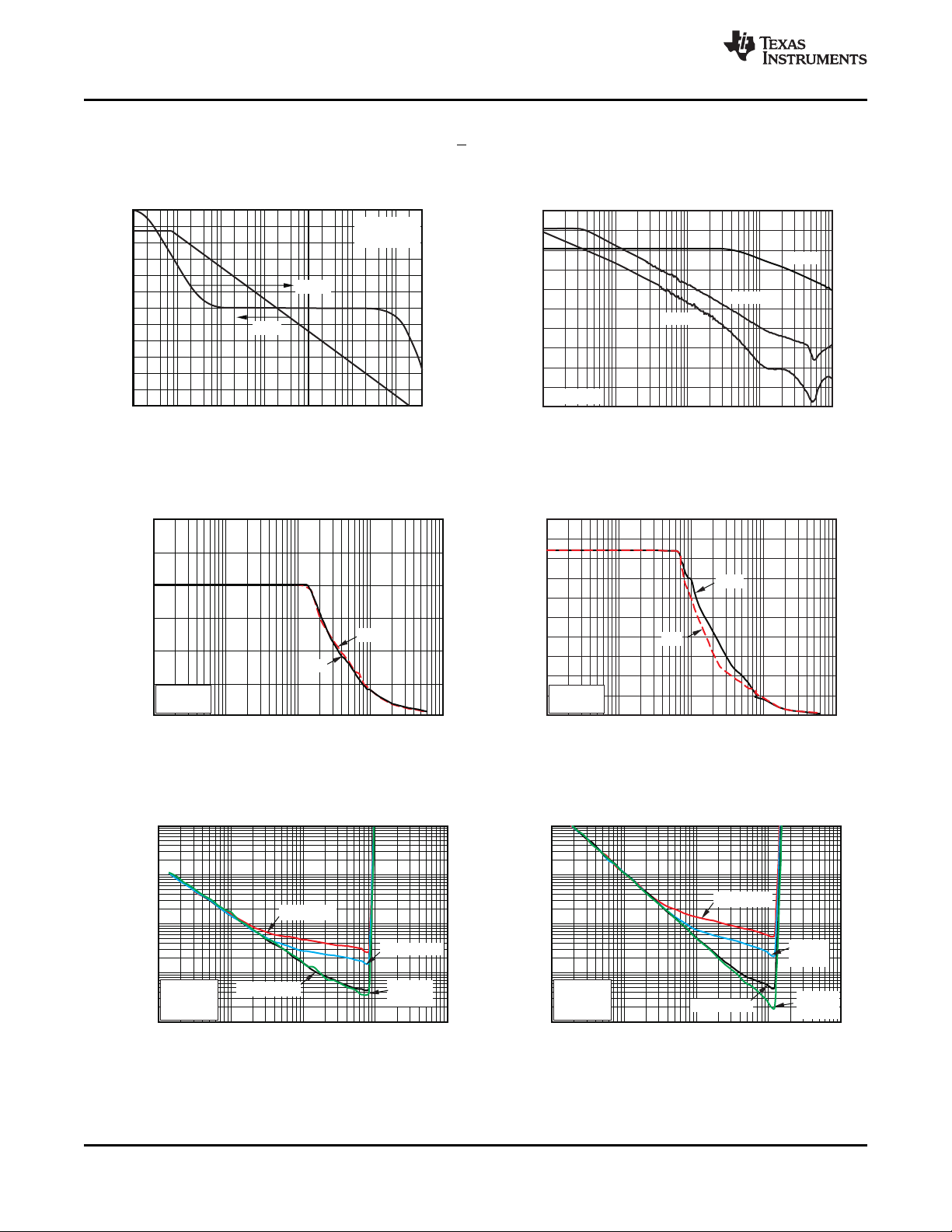
TYPICAL CHARACTERISTICS
At T
QUIESCENT CURRENT vs SUPPLY VOLTAGE OUTPUT VOLTAGE SWING vs OUTPUT CURRENT
LARGE−SIGNAL STEP RESPONSE, NO LOAD LARGE−SIGNAL STEP RESPONSE
= +25°C, VS= ±12V, R
CASE
Figure 1. Figure 2.
LOAD
www.ti.com
= 20kΩ to GND, and E/S pin enabled, unless otherwise noted.
Figure 3. Figure 4.
SMALL−SIGNAL STEP RESPONSE SMALL−SIGNAL OVERSHOOT vs LOAD CAPACITANCE
8 Submit Documentation Feedback Copyright © 2008–2009, Texas Instruments Incorporated
Figure 5. Figure 6.
Product Folder Link(s): OPA564
Page 9
50
45
40
35
30
25
20
QuiescentCurrent(mA)
-75
-50 -25 0 25 50
75
100 125
Temperature( C)
°
R =7.5kW
CL
20
15
10
5
0
5
10
15
20
-
-
-
-
OffsetVoltage(mV)
-75
-50 -25 0 25 50
75
100 125
Temperature( C)
°
2200
2000
1800
1600
1400
1200
1000
800
600
400
200
0
200-
InputBiasCurrent(pA)
-75
-50 -25 0 25 50
75
100 125
Temperature( C)
°
I
B+
I
B-
I
OS
300
250
200
150
100
50
0
50
100
150
200
250
300
-
-
-
-
-
-
Common-ModeRejectionRatio,Power-Supply
RejectionRatio,Open-LoopGain( V/V)m
-75
-50 -25 0 25 50
75
100 125
Temperature( C)
°
CMRR
PSRR
A
OL
2.0
1.5
1.0
0.5
0
QuiescentCurrent,Shutdown(mA)
-75
-50 -25 0 25 50
75
100 125
Temperature( C)
°
100
80
60
40
20
0
DigitalCurrent( A)m
-75
-50 -25 0 25 50
75
100 125
Temperature( C)
°
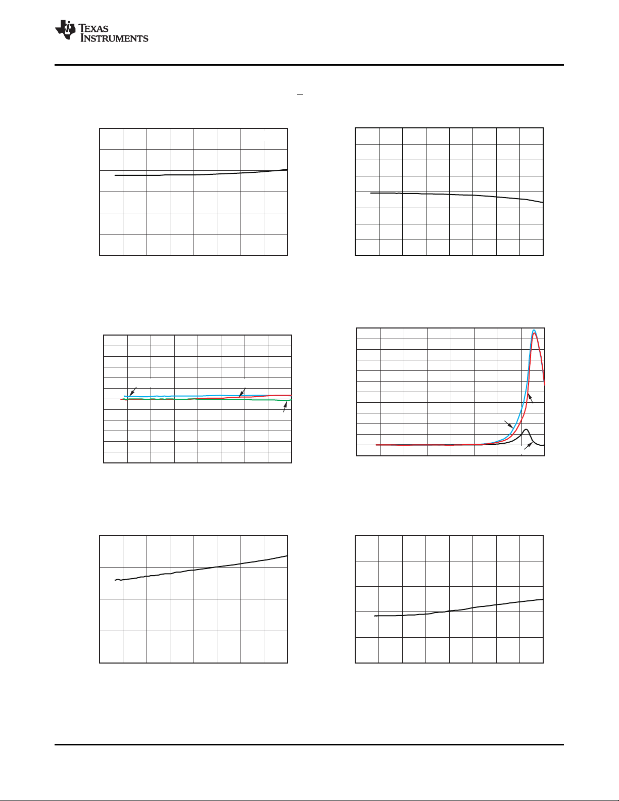
OPA564
www.ti.com
At T
CASE
SBOS372C –OCTOBER 2008–REVISED NOVEMBER 2009
TYPICAL CHARACTERISTICS (continued)
= +25°C, VS= ±12V, R
IQvs TEMPERATURE OFFSET VOLTAGE vs TEMPERATURE
Figure 7. Figure 8.
AOL, PSRR, AND CMRR vs TEMPERATURE IBvs TEMPERATURE
= 20kΩ to GND, and E/S pin enabled, unless otherwise noted.
LOAD
Copyright © 2008–2009, Texas Instruments Incorporated Submit Documentation Feedback 9
Figure 9. Figure 10.
IQ, SHUTDOWN vs TEMPERATURE I
Figure 11. Figure 12.
Product Folder Link(s): OPA564
vs TEMPERATURE
DIG
Page 10
120
100
80
60
40
20
0
Frequency(Hz)
Gain(dB)
0
-45
-90
-135
-180
Phase( )°
10k 100k 1M 10M 40M
V = 12V
R =1k
S
LOAD
±
W
Gain
Phase
10 100
1k
100
80
60
40
20
0
CMRR,PSRR(dB)
10 100
10k1k 100k
Frequency(Hz)
V = 12VS±
CMRR
-PSRR
+PSRR
15.0
12.5
10.0
7.5
5.0
2.5
0
OutputVoltage(V )
PP
10k 100k 1M 10M 100M
Frequency(Hz)
10W
100W
V = 12V
G=+1
S
±
25
20
15
10
5
0
OutputVoltage(V )
PP
10k 100k 1M 10M 100M
Frequency(Hz)
100W
10W
V = 12V
G=+1
S
±
0.01 0.1
1
10 100
1
0.1
0.01
0.001
0.0001
TotalHarmonicDistortion+Noise(%)
R =10
LOAD
W
R =5
LOAD
W
R =60
LOAD
W
R =
NoLoad
LOAD
V Amplitude(V )
OUT P
V = 12V
S
f=1kHz
G=+1
±
0.01 0.1
1
10 100
1
0.1
0.01
0.001
0.0001
TotalHarmonicDistortion+Noise(%)
R =
10
LOAD
W
R =5
LOAD
W
R =60
LOAD
W
R =
NoLoad
LOAD
V Amplitude(V )
OUT P
V = 12V
S
f=1kHz
G= 10-
±
OPA564
SBOS372C –OCTOBER 2008–REVISED NOVEMBER 2009
TYPICAL CHARACTERISTICS (continued)
At T
= +25°C, VS= ±12V, R
CASE
= 20kΩ to GND, and E/S pin enabled, unless otherwise noted.
LOAD
GAIN AND PHASE vs FREQUENCY POWER-SUPPLY REJECTION RATIO vs FREQUENCY
Figure 13. Figure 14.
OUTPUT VOLTAGE SWING vs FREQUENCY OUTPUT VOLTAGE SWING vs FREQUENCY
www.ti.com
COMMON-MODE REJECTION RATIO AND
Figure 15. Figure 16.
TOTAL HARMONIC DISTORTION + NOISE vs AMPLITUDE TOTAL HARMONIC DISTORTION + NOISE vs AMPLITUDE
10 Submit Documentation Feedback Copyright © 2008–2009, Texas Instruments Incorporated
Figure 17. Figure 18.
Product Folder Link(s): OPA564
Page 11

0.01 0.1
1
10 100
V Amplitude(V )
OUT P
1
0.1
0.01
0.001
0.0001
TotalHarmonicDistortion+Noise(%)
V = 12VS±
f=1kHz
G=+10
R =
10
LOAD
W
R =5
LOAD
W
R =60
LOAD
W
R =
NoLoad
LOAD
10 100
1k
10k 100k
Frequency(Hz)
1
0.1
0.01
0.001
0.0001
TotalHarmonicDistortion+Noise(%)
G=+10
V =8V
OUT P
R =
LOAD
10W
R =
LOAD
5W
R =
LOAD
60W
R =
LOAD
NoLoad
10 100
1k
10k 100k
Frequency(Hz)
1
0.1
0.01
0.001
0.0001
TotalHarmonicDistortion+Noise(%)
G= 10
V =8V
-
OUT P
R =
LOAD
10W
R =
LOAD
5W
R =
LOAD
60W
R =
LOAD
NoLoad
10 100
1k
10k 100k
Frequency(Hz)
1
0.1
0.01
0.001
0.0001
TotalHarmonicDistortion+Noise(%)
G=+1
V =5V
OUT P
R =
LOAD
10W
R =
LOAD
5W
R =
LOAD
60W
R =
LOAD
NoLoad
1k
100
10
1
1k
100
10
1
VoltageNoise(nV/ )Hz
Ö
CurrentNoise(fA/ )HzÖ
10 100
1k 10k 100k
Frequency(Hz)
V = 12VS±
VoltageNoise
CurrentNoise
10k
1k
100
10
1
Impedance( )W
1 10 100
1k 10k 100k 1M 10M 100M
Frequency(Hz)
I =0Adc
OUT
OPA564
www.ti.com
SBOS372C –OCTOBER 2008–REVISED NOVEMBER 2009
TYPICAL CHARACTERISTICS (continued)
At T
= +25°C, VS= ±12V, R
CASE
= 20kΩ to GND, and E/S pin enabled, unless otherwise noted.
LOAD
TOTAL HARMONIC DISTORTION + NOISE vs AMPLITUDE TOTAL HARMONIC DISTORTION + NOISE vs FREQUENCY
Figure 19. Figure 20.
TOTAL HARMONIC DISTORTION + NOISE vs FREQUENCY TOTAL HARMONIC DISTORTION + NOISE vs FREQUENCY
INPUT VOLTAGE SPECTRAL NOISE AND
Copyright © 2008–2009, Texas Instruments Incorporated Submit Documentation Feedback 11
Figure 21. Figure 22.
CURRENT NOISE vs FREQUENCY OPEN-LOOP OUTPUT IMPEDANCE (No Load)
Product Folder Link(s): OPA564
Figure 23. Figure 24.
Page 12

10k
1k
100
10
1
0.1
0.01
Impedance( )W
10 100
1k 10k 100k 1M 10M 100M
Frequency(Hz)
I =0Adc
Gain=1V/V
OUT
50
40
30
20
10
0
10-
InputBiasCurrent(pA)
-12
-10 -8 -6
-4 -2
0
2 4
6 8 10
Common-ModeVoltage(V )
CM
2V/div
Time(100ns/div)
R =10k
R =100
V = 6V
W
W
-
F
LOAD
OUT
V
OUT
E/S
V-
0V
V
OUT
CH1:
0V
CH2:
0V
E/S
Time(500 s/div)m
1V/div
R =100 ,G=+1
LOAD
W
V =1V
IN
R =10k
R =100
V = 6V
W
W
-
F
LOAD
OUT
2V/div
Time(1 s/div)m
V
OUT
E/S
V-
0V
60
50
40
30
20
10
0
10
20
30
40
-
-
-
-
CurrentLimitError(%)
10k 15k 20k 25k 30k 35k 40k 45k 50k 55k 60k
R ( )W
CL
Mean
Mean+3
Mean 3s- s
OPA564
SBOS372C –OCTOBER 2008–REVISED NOVEMBER 2009
TYPICAL CHARACTERISTICS (continued)
At T
= +25°C, VS= ±12V, R
CASE
= 20kΩ to GND, and E/S pin enabled, unless otherwise noted.
LOAD
CLOSED-LOOP OUTPUT IMPEDANCE (No Load) COMMON-MODE VOLTAGE
Figure 25. Figure 26.
ENABLE RESPONSE
R
= 100Ω SHUTDOWN TIME (INVERTING CONFIGURATION)
LOAD
www.ti.com
INPUT BIAS CURRENT vs
Figure 27. Figure 28.
ENABLE TIME (INVERTING CONFIGURATION) CURRENT LIMIT PERCENT ERROR vs R
12 Submit Documentation Feedback Copyright © 2008–2009, Texas Instruments Incorporated
Figure 29. Figure 30.
CL
Product Folder Link(s): OPA564
Page 13

1.8
1.6
1.4
1.2
1.0
0.8
0.6
0.4
0.2
0
OutputCurrentLimit(A)
10k 15k 20k 25k 30k 35k 40k 45k 50k 55k 60k
R ( )W
CL
Mean
Mean 3
Mean+3
CalculatedValue
- s
s
1.8
1.6
1.4
1.2
1.0
0.8
0.6
0.4
0.2
0
OutputCurrentLimit(A)
10k 15k 20k 25k 30k 35k 40k 45k 50k 55k 60k
R ( )W
CL
Mean
Mean 3
Mean+3
CalculatedValue
- s
s
5
4
3
2
1
0
I Increase(mA)
Q
5k
15k 25k 45k35k 55k 65k 75k
R ( )W
CL
Population
-18.0
-16.2
-14.4
-12.6
-10.8
-9.0
-7.2
-5.4
-3.6
-1.8
0
1.8
3.6
5.4
7.2
9.0
10.8
12.6
14.4
16.2
18.0
OffsetVoltage(mV)
OPA564
www.ti.com
At T
CASE
TYPICAL CHARACTERISTICS (continued)
= +25°C, VS= ±12V, R
OUTPUT CURRENT LIMIT vs R
(SOURCING CURRENT) (SINKING CURRENT)
Figure 31. Figure 32.
QUIESCENT CURRENT INCREASE vs R
= 20kΩ to GND, and E/S pin enabled, unless otherwise noted.
LOAD
SBOS372C –OCTOBER 2008–REVISED NOVEMBER 2009
CL
CL
OFFSET VOLTAGE PRODUCTION DISTRIBUTION
OUTPUT CURRENT LIMIT vs R
CL
Figure 33. Figure 34.
Copyright © 2008–2009, Texas Instruments Incorporated Submit Documentation Feedback 13
Product Folder Link(s): OPA564
Page 14

E/S
(2)
R
CL
(1)
47mF
0.1mF
V
O
VIN
V-
I
SET
OPA564
47mF
0.1mF
V
DIG
(3)
V+
Voltage(V)
Time(s)
Voltage(V)
Time(s)
Voltage(V)
Time(s)
(A) Sequencenotallowed
(1)
(B) Sequenceallowed
(C) Sequenceallowed
V
SUPPLY
V
SUPPLY
V
SUPPLY
V
DIGITAL
V
DIGITAL
V
DIGITAL
SeeNote1
OPA564
SBOS372C –OCTOBER 2008–REVISED NOVEMBER 2009
APPLICATION INFORMATION
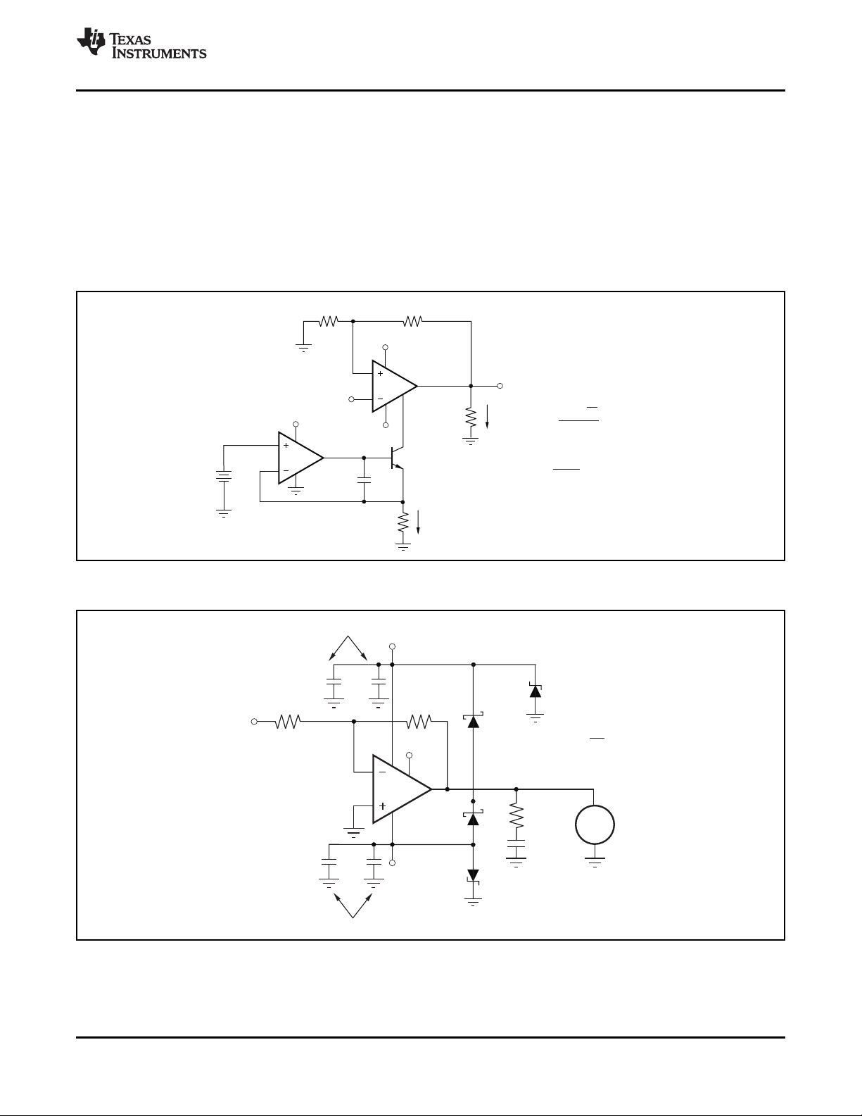
BASIC CONFIGURATION
Figure 35 shows the OPA564 connected as a basic
noninverting amplifier. However, the OPA564 can be
used in virtually any op amp configuration.
Power-supply terminals should be bypassed with low
series impedance capacitors. The technique of using
ceramic and tantalum capacitors in parallel is
recommended. Power-supply wiring should have low
series impedance.
www.ti.com
Sequencing of power supplies must assure that the
digital supply voltage (V
) be applied before the
DIG
supply voltage to prevent damage to the OPA564.
Figure 36 shows acceptable versus unacceptable
power-supply sequencing.
(1) RCLsets the current limit value from 0.4A to 1.5A.
(2) E/S pin forced low shuts down the output.
(3) V
of generating a signal for V
must not exceed (V–) + 5.5V; see Figure 53 for examples
DIG
DIG
.
Figure 35. Basic Noninverting Amplifier
POWER SUPPLIES
The OPA564 operates with excellent performance
from single (+7V to +24V) or dual (±3.5V to ±12V)
analog supplies and a digital supply of +3.3V to
+5.5V (referenced to the V– pin). Note that the
analog power-supply voltages do not need to be
symmetrical, as long as the total voltage remains
below 24V. For example, the positive supply could be
set to 14V with the negative supply at –10V. Most
behaviors remain constant across the operating
voltage range. Parameters that vary significantly with
operating voltage are shown in the Typical
Characteristics.
14 Submit Documentation Feedback Copyright © 2008–2009, Texas Instruments Incorporated
(1) The power-supply sequence illustrated in (A) is not allowed.
This power-supply sequence causes damage to the device.
Figure 36. Power-Supply Sequencing
Product Folder Link(s): OPA564
Page 15

RCL@
24kIW
LIM
- 5kW
I 20000x
LIM
@
1.2V
5000+R
CL
I 20,000
LIM
I
SET
@ ´
R
CL
OPA564
5kW
I
LIM
@
1.2V
R +5kW
CL
( )
´ 20k
V-
I
SET
1.2V
Bandgap
I I
OUT LIM
£
1nF
(optional,fornoisy
environments)
(1)
OPA564
www.ti.com
ADJUSTABLE CURRENT LIMIT
The OPA564 provides over-current protection to the
load through its accurate, user-adjustable current limit
(I
pin). The current limit value, I
SET
0.4A to 1.5A by controlling the current through the
I
pin. Setting the current limit does not require
SET
special power resistors. The output current does not
flow through the I
SET
pin.
A simple resistor to the negative rail is sufficient for a
general, coarse limit of the output current. Figure 30
exhibits the percent of error in the transfer function
between I
SET
and I
versus the current limit set
OUT
resistor, RCL; Figure 31 and Figure 32 show how this
error translates to variation in I
dotted line represents the ideal output current setting
which is determined by the following equation:
The mismatch errors between the current limit set
mirror and the output stage are primarily a result of
variations in the ~1.2V bandgap reference, an internal
5kΩ resistor, the mismatch between the current limit
and the output stage mirror, and the tolerance and
temperature coefficient of the RCLresistor referenced
to the negative rail. Additionally, an increase in
junction temperature can induce added mismatch in
accuracy between the I
SET
Figure 50 for a method that can be used to
dynamically change the current limit setting using a
simple, zero drift current source. This approach
simplifies the current limit equation to the following:
The current into the I
pin is determined by the
SET
NPN current source. Therefore, the errors contributed
by the internal 1.2V bandgap reference and the 5kΩ
resistor mismatch are eliminated, thus improving the
overall accuracy of the transfer function. In this case,
the primary source of error in I
tolerance and the beta of the NPN transistor.
It is important to note that the primary intent of the
current limit on the OPA564 is coarse protection of
the output stage; therefore, the user should exercise
caution when attempting to control the output current
by dynamically toggling the current limit setting.
Predictable performance is better achieved by
controlling the output voltage through the feedback
loop of the OPA564.
, can be set from
LIM
versus RCL. The
OUT
and I
SET
mirror. See
OUT
is the RCLresistor
(1)
(2)
SBOS372C –OCTOBER 2008–REVISED NOVEMBER 2009
Setting the Current Limit
Leaving the I
device. Connecting I
pin unconnected damages the
SET
directly to V– is not
SET
recommended because it programs the current limit
far beyond the 1.5A capability of the device and
causes excess power dissipation. The minimum
recommended value for RCLis 7.5kΩ, which
programs the maximum current limit to approximately
1.9A. The maximum value for RCLis 60kΩ, which
programs the minimum current limit to approximately
0.4A. The simplest method for adjusting the current
limit (I
between the I
If I
) uses a resistor or potentiometer connected
LIM
has been defined, RCLcan be solved by
LIM
pin and V–, according to Equation 1.
SET
rearranging Equation 1 into Equation 3:
(3)
RCLin combination with a 5kΩ internal resistor
determines the magnitude of a small current that sets
the desired output current limit.
Figure 37 shows a simplified schematic of the
OPA564 current limit architecture.
(1) At power-on, this capacitor is not charged. Therefore, the
OPA564 is programmed for maximum output current. Capacitor
values > 1nF are not recommended.
Figure 37. Adjustable Current Limit
Copyright © 2008–2009, Texas Instruments Incorporated Submit Documentation Feedback 15
Product Folder Link(s): OPA564
Page 16

Optocoupler
4N38
E/S
V+
(a) +5V
(b) HCTorTTLIn
HCTor
TTLIn
(a) (b)
OPA564
(1)
V-
500
450
400
350
300
250
200
150
100
50
0
OutputCurrent(pA)
-10 -8 -6
-4
-2 0 2
4
6 8 10
OutputVoltage(V)
V = 12VS±
OUTPUTSHUTDOWNOUTPUTVOLTAGEvsOUTPUTCURRENT
OPA564
E/ =Low(OutputShutdown)S
V
OUT
I
OUT
TestCircuit
OPA564
SBOS372C –OCTOBER 2008–REVISED NOVEMBER 2009
www.ti.com
ENABLE/SHUTDOWN (E/S) PIN Thus, in a dual-supply system, to shut down the
The output of the OPA564 shuts down when the E/S
pin is forced low. For normal operation (output
enabled), the E/S pin must be pulled high (at least 2V
above V–). To enable the OPA564 permanently, the
E/S pin can be left unconnected. The E/S pin has an
internal 100kΩ pull-up resistor. When the output is
shut down, the output impedance of the OPA564 is
6GΩ || 120pF. The output shutdown output voltage
versus output current is shown in Figure 39. Although
the output is high-impedance when shut down, there
is still a path through the feedback network into the
input stage to ground; see Figure 40. To prevent
damage to the OPA564, ensure that the voltage
across the internal protection diodes does not exceed
0.4V and the current flowing through the input
terminals does not exceed 10mA.
Output Shutdown
The shutdown pin (E/S) is referenced to the negative
supply (V–). Therefore, shutdown operation is slightly
different in single-supply and dual-supply
applications. In single-supply operation, V– typically
equals common ground. Therefore, the shutdown
logic signal and the OPA564 shutdown pin are
referenced to the same potential. In this configuration,
the logic pin and the OPA564 enable can simply be
connected together. Shutdown occurs for voltage
levels of less than 0.8V. The OPA564 is enabled at To shut down the output, the E/S pin is pulled low, no
logic levels greater than 2V. In dual-supply operation, greater than 0.8V above V–. This function can be
the logic pin remains referenced to a logic ground. used to conserve power during idle periods. To return
However, the shutdown pin of the OPA564 continues the output to an enabled state, the E/S pin should be
to be referenced to V–. pulled to at least 2.0V above V–. Figure 27 shows the
OPA564 the voltage level of the logic signal must be
level-shifted by some means. One way to shift the
logic signal voltage level is by using an optocoupler,
as Figure 38 shows.
(1) Optional; may be required to limit leakage current of
optocoupler at high temperatures.
Figure 38. Shutdown Configuration for Dual
Supplies (Using Optocoupler)
typical enable and shutdown response times. It
should be noted that the E/S pin does not affect the
internal thermal shutdown.
16 Submit Documentation Feedback Copyright © 2008–2009, Texas Instruments Incorporated
Figure 39. Output Shutdown Output Impedance
Product Folder Link(s): OPA564
Page 17

R
F
1.6kW
1.6kW
6GW
R
1
120pF
V+
V+
V+
V+
V-
V-
V-
V-
V
OUT
OPA564
www.ti.com
SBOS372C –OCTOBER 2008–REVISED NOVEMBER 2009
Figure 40. OPA564: Output Shutdown Equivalent Circuit (with External Feedback)
operating within the limits set by the user. A voltage
Ensuring Microcontroller Compatibility
Not all microcontrollers output the same logic state
after power-up or reset. 8051-type microcontrollers,
for example, output logic high levels while other
models power up with logic low levels after reset. In
the configuration of Figure 38 (a), the shutdown
signal is applied on the cathode side of the
photodiode within the optocoupler. A high logic level
causes the OPA564 to be enabled, and a low logic
level shuts the OPA564 down. In the configuration of
Figure 38 (b), with the logic signal applied on the
anode side, a high level causes the OPA564 to shut
down, and a low level enables the op amp.
level of +2.0V or greater with respect to V– indicates
that the OPA564 is operating above (exceeds) the
current limit set by the user. See Setting the Current
Limit for proper current limit operation.
OUTPUT STAGE COMPENSATION
The complex load impedances common in power op
amp applications can cause output stage instability.
For normal operation, output compensation circuitry is
typically not required. However, if the OPA564 is
intended to be driven into current limit, an R/C
network (snubber) may be required. A snubber circuit
such as the one shown in Figure 51 may also
enhance stability when driving large capacitive loads
CURRENT LIMIT FLAG
The OPA564 features a current limit flag (I
can be monitored to determine if the load current is
) that
FLAG
operating within or exceeding the current limit set by
the user. The output signal of I
standard CMOS logic and is referenced to the
negative supply pin (V–). A voltage level of + 0.8V or
less with respect to V– indicates that the amplifier is
is compatible with
FLAG
(greater than 1000pF) or inductive loads (for
example, motors or loads separated from the
amplifier by long cables). Typically, 3Ω to 10Ω in
series with 0.01μF to 0.1μF is adequate. Some
variations in circuit value may be required with certain
loads.
Copyright © 2008–2009, Texas Instruments Incorporated Submit Documentation Feedback 17
Product Folder Link(s): OPA564
Page 18

1.6
1.4
1.2
1.0
0.8
0.6
0.4
0.2
0
MaxI (A)
OUT
-50 -25 0 25 50
75
100 125
T ( C)
J
°
MaxI (dc)
MaxI (RMS)
OUT
OUT
MAXIMUMOUTPUTCURRENTvsJUNCTIONTEMPERATURE
OPA564
SBOS372C –OCTOBER 2008–REVISED NOVEMBER 2009
www.ti.com
OUTPUT PROTECTION triggers. Use worst-case loading and signal
The output structure of the OPA564 includes ESD
diodes (see Figure 40). Voltage at the OPA564
output must not be allowed to go more than 0.4V
beyond either supply rail to avoid damaging the
device. Reactive and electromagnetic field The internal protection circuitry of the OPA564 was
(EMF)-generation loads can return load current to the designed to protect against overload conditions; it
amplifier, causing the output voltage to exceed the was not intended to replace proper heatsinking.
power-supply voltage. This damaging condition can Continuously running the OPA564 into thermal
be avoided with clamping diodes from the output shutdown degrades reliability.
terminal to the power supplies, as Figure 51 and
Figure 52 illustrate. Schottky rectifier diodes with a 3A
or greater continuous rating are recommended.
conditions. For good, long-term reliability, thermal
protection should trigger more than 35°C above the
maximum expected ambient condition of the
application.
THERMAL PROTECTION
The OPA564 has thermal sensing circuitry that helps
protect the amplifier from exceeding temperature
limits. Power dissipated in the OPA564 causes the
junction temperature to rise. Internal thermal
shutdown circuitry disables the output when the die
temperature reaches the thermal shutdown
temperature limit. The OPA564 output remains shut
down until the die has cooled sufficiently; see the
Electrical Characteristics, Thermal Shutdown section.
Depending on load and signal conditions, the thermal
protection circuit may cycle on and off. This cycling
limits the amplifier dissipation, but may have
undesirable effects on the load. Any tendency to
activate the thermal protection circuit indicates Temperature
excessive power dissipation or an inadequate
heatsink. For reliable, long-term, continuous
operation, with I
at the maximum output of 1.5A,
OUT
the junction temperature should be limited to +85°C
maximum. Figure 41 shows the maximum output
current versus junction temperature for dc and RMS
signal outputs. To estimate the margin of safety in a
complete design (including heatsink), increase the
ambient temperature until the thermal protection
Figure 41. Maximum Output Current vs Junction
USING T
FOR MEASURING JUNCTION
SENSE
TEMPERATURE
The OPA564 includes an internal diode for junction
temperature monitoring. The η-factor of this diode is
1.085. Measuring the OPA564 junction temperature
can be accomplished by connecting the T
a remote-junction temperature sensor, such as the
TMP411 (see Figure 54).
SENSE
pin to
18 Submit Documentation Feedback Copyright © 2008–2009, Texas Instruments Incorporated
Product Folder Link(s): OPA564
Page 19

10.0
1.0
0.1
OutputCurrent(A)
0 2
4
6 8 10 12 14 16 18 20 22 24 26
(V+) V , (V )(V)-
OUTVOUT
- -
SAFEOPERATINGAREAATROOMTEMPERATURE
Copper,Soldered
withoutForcedAir
Copper,Soldered
with200LFMAirflow
10.0
1.0
0.1
0.01
OutputCurrent(A)
0 2
4
6 8 10 12 14 16 18 20 22 24 26
SAFEOPERATINGAREAATVARIOUSAMBIENTTEMPERATURES
(PowerPADSoldered)
T = 40 C-
A
T =0 C
T =+25 C
T =+85 C
T =+125 C
A
A
A
A
°
°
°
°
°
(V+) V , (V )(V)-
OUTVOUT
- -
OPA564
www.ti.com
POWER DISSIPATION AND SAFE OPERATING AREA
Power dissipation depends on power supply, signal,
and load conditions. For dc signals, power dissipation
is equal to the product of output current (I
voltage across the conducting output transistor [(V+)
– V
Dissipation with ac signals is lower. Application
Bulletin AB-039, Power Amplifier Stress and Power
Handling Limitations (SBOA022, available for
download from www.ti.com) explains how to calculate
or measure power dissipation with unusual signals
and loads.
Figure 42 shows the safe operating area at room
temperature with various heatsinking efforts. Note
that the safe output current decreases as (V+) – V
or V
operating area at various temperatures with the
PowerPAD being soldered to a 2oz copper pad.
The power that can be safely dissipated in the
package is related to the ambient temperature and
the heatsink design. The PowerPAD package was
specifically designed to provide excellent power
dissipation, but board layout greatly influences the
heat dissipation of the package. Refer to the
Thermally-Enhanced PowerPAD Package section for
further details.
The relationship between thermal resistance and
power dissipation can be expressed as:
TJ= TA+ T
TJA= PD× θ
Combining these equations produces:
TJ= TA+ PD× θ
where:
TJ= Junction temperature (°C)
TA= Ambient temperature (°C)
θ
JA
PD= Power dissipation (W)
To determine the required heatsink area, required
power dissipation should be calculated and the
relationship between power dissipation and thermal
resistance should be considered to minimize
shutdown conditions and allow for proper long-term
operation (junction temperature of +85°C or less).
Once the heatsink area has been selected,
worst-case load conditions should be tested to ensure
proper thermal protection.
space
Copyright © 2008–2009, Texas Instruments Incorporated Submit Documentation Feedback 19
when sourcing; V
OUT
– (V–) increases. Figure 43 shows the safe
OUT
JA
JA
JA
– (V–) when sinking].
OUT
= Junction-to-ambient thermal resistance (°C/W)
SBOS372C –OCTOBER 2008–REVISED NOVEMBER 2009
) and the
OUT
OUT
Figure 42. Safe Operating Area at Room
Temperature
PowerPAD soldered to a 2oz copper pad.
Figure 43. Safe Operating Area at Various
Ambient Temperatures
Product Folder Link(s): OPA564
Page 20

45
40
35
30
25
20
ThermalResistance, ( C/W)°
JA
0 1
q
2 3 4 5
CopperArea(inches )
2
OPA564
SurfaceMountPackage
2ozcopper
THERMALRESISTANCEvsCIRCUITBOARDCOPPERAREA
6
5
4
3
2
1
0
PowerDissipationinPackage(W)
0 25 50
75
100 125
Temperature( C)
°
NoCopper
Copper,Soldered
withoutForcedAir
Copper,Soldered
with200LFMAirflow
MAXIMUMPOWERDISSIPATIONvsTEMPERATURE
OPA564
SBOS372C –OCTOBER 2008–REVISED NOVEMBER 2009
For applications with limited board size, refer to THERMALLY-ENHANCED PowerPAD
Figure 44 for the approximate thermal resistance PACKAGE
relative to heatsink area. Increasing heatsink area
beyond 2in2provides little improvement in thermal
resistance. To achieve the 33°C/W shown in the
Electrical Characteristics, a 2oz copper plane size of
9in2was used. The PowerPAD package is well-suited
for continuous power levels from 2W to 4W,
depending on ambient temperature and heatsink
area. The addition of airflow also influences maximum
power dissipation, as Figure 45 illustrates. Higher
power levels may be achieved in applications with a
low on/off duty cycle, such as remote meter reading.
The OPA564 uses the HSOP-20 PowerPAD DWP
and DWD, and the HTSSOP-20 PWP packages,
which are thermally-enhanced, standard size IC
packages. These packages enhance power
dissipation capability significantly and can be easily
mounted using standard printed circuit board (PCB)
assembly techniques, and can be removed and
replaced using standard repair procedures.
The PWP and DWP PowerPAD packages are
designed so that the leadframe die pad (or thermal
pad) is exposed on the bottom of the IC, as shown in
Figure 46 a; the DWD PowerPAD package has the
exposed pad on the top side of the package, as
shown in Figure 46 b. The thermal pad provides an
extremely low thermal resistance (θJC) path between
the die and the exterior of the package.
PowerPAD packages with exposed pad down are
designed to be soldered directly to the PCB, using
the PCB as a heatsink. Texas Instruments does not
recommend the use of the of a PowerPAD package
without soldering it to the PCB because of the risk of
lower thermal performance and mechanical integrity.
In addition, through the use of thermal vias, the
bottom-side thermal pad can be directly connected to
a power plane or special heatsink structure designed
into the PCB. The PowerPAD should be at the same
voltage potential as V–. Soldering the bottom-side
Figure 44. Thermal Resistance vs Circuit Board
Copper Area
PowerPAD to the PCB is always required, even with
applications that have low power dissipation. It
provides the necessary thermal and mechanical
connection between the leadframe die and the PCB.
Pad-up PowerPAD packages should have
appropriately designed heatsinks attached. Because
of the variation and flexible nature of this type of heat
sink, additional details should come from the specific
manufacturer of the heatsink.
www.ti.com
20 Submit Documentation Feedback Copyright © 2008–2009, Texas Instruments Incorporated
Figure 45. Maximum Power Dissipation vs
Temperature
Product Folder Link(s): OPA564
Page 21

MoldCompound(Epoxy)
LeadframeDiePad
ExposedatBaseofthePackage
Leadframe(CopperAlloy)
(a) DWPandPWPPowerPADcross-sectionview
(b) DWDPowerPADcross-sectionview
IC(Silicon)
DieAttach(Epoxy)
Board
ExternalHeatspreader
Power Transistor
Chip
Die
Attach
Thermal
Paste
Die
Pad
WeborSpokeViaSolidVia
NOTRECOMMENDEDRECOMMENDED
OPA564
www.ti.com
SBOS372C –OCTOBER 2008–REVISED NOVEMBER 2009
Figure 46. Cross-Section Views
holes under the PowerPAD package should be
Bottom-Side PowerPAD Assembly Process
connected to the internal plane with a complete
1. The PowerPAD must be connected to the most connection around the entire circumference of the
negative supply of the device, V–. plated through-hole.
2. Prepare the PCB with a top side etch pattern, as 7. The top-side solder mask should leave exposed
shown in the attached thermal land pattern the terminals of the package and the thermal pad
mechanical drawing. There should be etch for the area. The thermal pad area should leave the
leads as well as etch for the thermal land. 13mil holes exposed. The larger 25mil holes
3. Place the recommended number of holes (or
thermal vias) in the area of the thermal pad, as
outside the thermal pad area should be covered
with solder mask.
seen in the attached thermal land pattern 8. Apply solder paste to the exposed thermal pad
mechanical drawing. These holes should be area and all of the package terminals.
13mils (.013in, or 330.2μm) in diameter. They are
kept small so that solder wicking through the
holes is not a problem during reflow.
9. With these preparatory steps completed, the
PowerPAD IC is simply placed in position and run
through the solder reflow operation as any
4. It is recommended, but not required, to place a standard surface-mount component. This
small number of the holes under the package and processing results in a part that is properly
outside the thermal pad area. These holes installed.
provide an additional heat path between the
copper land and ground plane and are 25mils
(.025in, or 635μm) in diameter. They may be
larger because they are not in the area to be
soldered, so wicking is not a problem. This
configuration is illustrated in the attached thermal
For detailed information on the PowerPAD package
including thermal modeling considerations and repair
procedures, see Technical Brief SLMA002,
PowerPAD Thermally Enhanced Package, available
at www.ti.com.
land pattern mechanical drawing.
5. Connect all holes, including those within the
thermal pad area and outside the pad area, to the
internal plane that is at the same voltage potential
as V–.
6. When connecting these holes to the internal
plane, do not use the typical web or spoke via
connection methodology (as Figure 47 shows).
Web connections have a high thermal resistance
connection that is useful for slowing the heat
transfer during soldering operations. This
configuration makes the soldering of vias that
have plane connections easier. However, in this
application, low thermal resistance is desired for
the most efficient heat transfer. Therefore, the
Copyright © 2008–2009, Texas Instruments Incorporated Submit Documentation Feedback 21
Figure 47. Via Connection Methods
Product Folder Link(s): OPA564
Page 22

OPA564
I
SET
47mF
R
2
1kW
R
1
20kW
R
4
1kW
R
4
20kW
R
5
50mW
V
O
-5V
+1V/+1A
V
DIG
+5V
0.1 Fm
0.1 Fm
47 Fm
R
CL
R
3
OPA564
C
5
+
C
6
R
1
C
1
C
10pF
4
R
F
C
F
C
47 Fm
3
C
0.1 Fm
2
3
4
6
1
T
1
D
1
SMBJ12CA
L
1
S
1
S
3
S
4
S
2
V
S
V
DIG
INPUT
1/2V
S
E/S
GND
OPA564
SBOS372C –OCTOBER 2008–REVISED NOVEMBER 2009
www.ti.com
APPLICATIONS CIRCUITS POWERLINE COMMUNICATION
The high output current and low supply of the Powerline communication (PLC) applications require
OPA564 make it a good candidate for driving laser some form of signal transmission over an existing ac
diodes and thermoelectric coolers. Figure 48 shows power line. A common technique used to couple
an improved Howland current pump circuit. these modulated signals to the line is through a signal
transformer. A power amplifier is often needed to
provide adequate levels of current and voltage to
drive the varying loads that exist on today’s
powerlines. One such application is shown in
Figure 49. The OPA564 is used to drive signals used
in frequency modulation schemes such as FSK
(Frequency-Shift Keying) or OFDM (Orthogonal
Frequency-Division Multiplexing) to transmit digital
information over the powerline. The power output
capabilities of the OPA564 are needed to drive the
current requirements of the transformer that is shown
in the figure, coupled to the ac power line via a
coupling capacitor. Circuit protection is often needed
or required to prevent excessive line voltages or
current surges from damaging the active circuitry in
the power amplifier and application circuitry.
(1) See Figure 35 for an example of a basic noninverting amplifier
with V
not exceeding 5.5V.
DIG
Figure 48. Improved Howland Current Pump
(1) S1, S2, S3, and S4are Schottky diodes. D1is a transient suppression diode.
(2) L1should be small enough so that it does not interfere with the bandwidth of interest but large enough to suppress transients that could
damage the OPA564.
22 Submit Documentation Feedback Copyright © 2008–2009, Texas Instruments Incorporated
Figure 49. Powerline Communication Line Coupling
Product Folder Link(s): OPA564
Page 23
R
1
R
F
T1
2N2923
+
+5V
V+
V-
I
SET
I
SET
I
OUT
V
OUT
V
IN
V
SET
R
LOAD
OPA564
OPA333
R
5kCLW
C
100pF
1
V
100mV
SET
V (1+)
IN
R
R
F
1
R
LOAD
I =
OUT
£ I
LIM
I I
LIM SET
20,000
@ ´
I
SET
@
I
20,000
LIM
I
SET
(0.4Ato1.5A)=20 Ato75 Am m
V
SET
(0.4Ato1.5A)=100mVto375mV
and
G= - = -4
R
2
R
1
V
IN
V+
V
DIG
V-
R
1
5kW
R
2
20kW
OPA564
10W
(Noninductive)
Motor
0.01 Fm
Z
1
(1)
Z
2
S
2
S
1
(1)
(2)
(2)
C
0.1 F1m
C
0.1 F1m
C
47 F2m
C
47 F2m
Note(3)
Note(3)
OPA564
www.ti.com
SBOS372C –OCTOBER 2008–REVISED NOVEMBER 2009
PROGRAMMABLE POWER SUPPLY For more information on this circuit, see the
Figure 50 shows the OPA333 used to control I
SET
in
order to adjust the current limit of the OPA564.
Figure 51 shows a basic motor speed driver but does
not include any control over the motor speed. For
applications where good control of the speed of the
motor is desired, but the precision of a tachometer
control is not required, the circuit in Figure 52
provides control by using feedback of the current
consumption to adjust the motor drive.
Application Bulletin DC Motor Speed Controller:
Control a DC Motor without Tachometer Feedback
(SBOA043), available for download at the TI web site.
Figure 53 shows two examples of generating the
signal for V
to bias the V
b uses a high-voltage subregulator to derive the V
. Figure 53 a uses an 1N4732A zener
DIG
to precisely 4.7V above V–. Figure 53
DIG
DIG
voltage. Figure 55 illustrates a detailed powerline
communication circuit.
Figure 50. Programmable Current Limit Option
(1) Z1, Z2= zener diodes (IN5246 or equivalent).
(2) S1, S2= Schottky diodes (POS5100h-13 or equivalent).
(3) C1 = high-frequency bypass capacitors; C2= low-frequency bypass capacitors (minimum of 10μF for every 1A peak current)
Copyright © 2008–2009, Texas Instruments Incorporated Submit Documentation Feedback 23
Figure 51. Motor Drive Circuit
Product Folder Link(s): OPA564
Page 24

+12V
-12V
R
M
R =12W
M
dc
Motor
R
2
10kW
R
1
1kW
R
CL
V
IN
EMF
R
S
1W
OPA564
V
DIG
(1)
C
0.1 F1m
C
0.1 F1m
C
47 F2m
C
47 F2m
R
5k3W
Z
2
S
2
Z
1
S
1
(2)
(2)
(3)
(3)
Note(4)
Note(4)
V+
V-
V
DIG
10kW
4.7V
Zener
1N4732A
(a)
(b)
2
51
4
3
IN
C
1000 Fm
I1
C
100nF
I2
C
22 Fm
OUT
I
IN
I
RO
V
RD
V
OUT
I
OUT
R
EXT
5kW
V
IN
I
D,cID,d
I
GND
V
D
C
D
47nF
DELAY
GND
RESET
OUT
TLE4275-Q1
OPA564
SBOS372C –OCTOBER 2008–REVISED NOVEMBER 2009
www.ti.com
(1) I
FLAG
and T
connections are not shown.
FLAG
(2) Z1, Z2= zener diodes (IN5246 or equivalent).
(3) S1, S2= Schottky diodes (POS5100h-13 or equivalent).
(4) C1= high-frequency bypass capacitors; C2= low-frequency bypass capacitors (minimum of 10μF for every 1A peak current).
Figure 52. DC Motor Speed Controller (without Tachometer)
Figure 53. Circuits for Generating V
Product Folder Link(s): OPA564
DIG
24 Submit Documentation Feedback Copyright © 2008–2009, Texas Instruments Incorporated
Page 25

T
SENSE
50W
V-
50pF
D-
D+
SCL
SDA
ALERTTHERM2/
THERM
GND
V+
+5V
0.1 Fm
10k
(typ)
W 10k
(typ)
W 10k
(typ)
W 10k
(typ)
W
SMBus
Controller
Over-Temperature
Fault
OPA564
TMP411
1
8
7
6
4
5
3
2
-IN
V+
V
DIG
+IN
V
OUT
4
3
1
5
2
U3
OPA365
4
3
1
5
2
U5
OPA365
4
3
1
5
2
U9
OPA365
4
3
1
5
2
U11
OPA365
AVDD
1
CH1
2
CH0/VCAL
3
Vref
4
Vout5GND
6
SCLK
7
DIO
8
NOTCS
9
DVDD
10
U10
PGA112
V-
1
V+
2
TFLG
3
E/S
4
+IN
5
-IN
6
VDIG
7
IFLAG
8
ISET
9
V-10V-
11
TSENSE
12
V-pwr
13
V-pwr
14
Vout
15
Vout
16
V+pwr
17
V+pwr
18
V+pwrSence
19
V-
20
Gnd
21
Gnd
22
Gnd
23
Gnd
24
Gnd
25
Gnd
26
Gnd
27
Gnd28Gnd
29
Gnd
30
Gnd
31
Gnd
32
Gnd
33
Gnd
34
Gnd
35
PowerPad OPA564
U4
OPA564AIDWP
1
2
3
4
5
6
7
8
9
10
11
12
J2
12HEADER
1
2
3
4
5
6
7
8
9
10
11
12
J3
12HEADER
R8
16.5k
R11
16.5k
R13
1.5k
R6
82.0k
R10
3.92k
R14
270ohm
R7
82.0k
R12
1.21k
C1
820pF
C11
TBD
C7
82pf
C5
2700pF
C8
270pF
C9
1.0uF
C2
0.1uF
R9
82.0k
R16
10.0k
R19
4.99k
R18
10.0k
R23
10.0k
R22
10.0k
R21
1.0ohms
C3
1200pf
C10
120pf
C4
0.1uF
C13
0.1uF
C16
0.1uF
R15
332ohm
C17
0.1uF
C19
10uF
C18
0.1uF
C20
0.1uF
R17
47.5k
R20
0.5ohm
R25
0ohm
R24
3.09k
C14
10uF
L1
LB3218T1ROM
D5
B350A-13-F
D4
B350A-13-F
TestPoint
1
TP1
TESTPOINT
TestPoint
1
TP8
TESTPOINT
TestPoint
1
TP2
TESTPOINT
TestPoint
1
TP3
TESTPOINT
TestPoint
1
TP4
TESTPOINT
1
2
JP5
JUMPER
R31
8.25k
R34
1.5k
R28
82.0k
R32
3.92k
R35
270ohm
R29
82.0k
R36
332ohm
R30
82.0k
R42
10.0k
R44
4.32k
R39
10.0k
R37
10.0k
R38
1.0k
R33
1.21k
R41
0.0ohm
C23
820pf
C29
82pf
C24
2700pf
C30
270pf
C31
1.0uF
C27
1200pf
C32
120pf
C33
47000pf
C28
0.1uF
C26
0.1uF
C38
0.1uF
C39
0.1uF
C35
0.1uf
C36
0.1uF
C37
0.1uF
D6
B350A-13-F
D7
B350A-13-F
D8B350A-13-F D9
B350A-13-F
C34
2700pf
R43
1.0ohms
GND
GND
D2
LED
D3
LED
D1
LED
R4
228ohm
R3
228ohm
R5
228ohm
GND
GND
GND
C12
2700pF
C15
TBD
GND
GND
GND
GND
GND
GND
GND
GND
GND
GND
GND
GND
GND
GND
GND
GND
GND
GND
GND
PWM2_GPIO02
PWM1_GPIO00
ADCIN
ADCIN
GND
+12V
SPISTEA_GPIO19
SPICLKA_GPIO18
TXRX
TXDRVEN_GPIO32
LEDGPIO20
LEDGPIO21
LEDGPIO22
R26
100ohm
C21
12000pf
L2
470uH
R27
499ohm
C22
18000pf
L3
330uH
GND
TXRX
C40
10uF
SPISIMOA_GPIO16
SPISOMIA_GPIO17
R45
0ohm
R47
10k
R46
10k
R48
10k
R49
10k
SPISTEA_GPIO19
SPICLKA_GPIO18
TXDRVEN_GPIO32
SPISIMOA_GPIO16
SPISOMIA_GPIO17
TestPoint
1
TP6
TESTPOINT
TestPoint
1
TP7
TESTPOINT
TestPoint
1
TP5
TESTPOINT
+3.3V
+5V
+5V
+5V
+5V
+5V
+5V
+5V
+5V
+5V
+5V
+5V
+3.3V
+3.3V
+3.3V
+3.3V
+12V
+12V
GND
TestPoint
1
Gnd
TESTPOINT
R50
10k
4
3
1
5
2
U2
OPA365
C6
0.1uF
GND
GND
+5V
4
3
1
5
2
U1
OPA365
4
3
1
5
2
U6
OPA365
4
3
1
5
2
U7
OPA365
C25
0.1uF
GND
GND
+5V
Pad
1
P1
FREEPAD
Pad
1
P2
FREEPAD
GND
Heatsink Pads
D11
MURS160-13
D10
MURS160-13
OPA564
www.ti.com
Figure 54. Temperature Measurement Using T
SBOS372C –OCTOBER 2008–REVISED NOVEMBER 2009
and TMP411
SENSE
Copyright © 2008–2009, Texas Instruments Incorporated Submit Documentation Feedback 25
Figure 55. Detailed Powerline Communication Circuit
Product Folder Link(s): OPA564
Page 26

OPA564
SBOS372C –OCTOBER 2008–REVISED NOVEMBER 2009
www.ti.com
REVISION HISTORY
NOTE: Page numbers for previous revisions may differ from page numbers in the current version.
Changes from Revision B (November, 2009) to Revision C Page
• Changed orderable device of OPA564 DWD package ......................................................................................................... 2
• Updated Thermal Resistance section of Electrical Characteristics table to differentiate performance characteristics
of available device packages ................................................................................................................................................ 5
26 Submit Documentation Feedback Copyright © 2008–2009, Texas Instruments Incorporated
Product Folder Link(s): OPA564
Page 27

PACKAGE OPTION ADDENDUM
www.ti.com
9-Aug-2010
PACKAGING INFORMATION
Orderable Device
OPA564AIDWD ACTIVE HSOP DWD 20 25 Green (RoHS
OPA564AIDWDR ACTIVE HSOP DWD 20 2000 Green (RoHS
OPA564AIDWP ACTIVE SO PowerPAD DWP 20 25 Green (RoHS
OPA564AIDWPR ACTIVE SO PowerPAD DWP 20 2000 Green (RoHS
(1)
The marketing status values are defined as follows:
ACTIVE: Product device recommended for new designs.
LIFEBUY: TI has announced that the device will be discontinued, and a lifetime-buy period is in effect.
NRND: Not recommended for new designs. Device is in production to support existing customers, but TI does not recommend using this part in a new design.
PREVIEW: Device has been announced but is not in production. Samples may or may not be available.
OBSOLETE: TI has discontinued the production of the device.
Status
(1)
Package Type Package
Drawing
Pins Package Qty
Eco Plan
& no Sb/Br)
& no Sb/Br)
& no Sb/Br)
& no Sb/Br)
(2)
Lead/
Ball Finish
CU NIPDAU Level-2-260C-1 YEAR Purchase Samples
CU NIPDAU Level-2-260C-1 YEAR Request Free Samples
CU NIPDAU Level-2-260C-1 YEAR Purchase Samples
CU NIPDAU Level-2-260C-1 YEAR Request Free Samples
MSL Peak Temp
(3)
Samples
(Requires Login)
(2)
Eco Plan - The planned eco-friendly classification: Pb-Free (RoHS), Pb-Free (RoHS Exempt), or Green (RoHS & no Sb/Br) - please check http://www.ti.com/productcontent for the latest availability
information and additional product content details.
TBD: The Pb-Free/Green conversion plan has not been defined.
Pb-Free (RoHS): TI's terms "Lead-Free" or "Pb-Free" mean semiconductor products that are compatible with the current RoHS requirements for all 6 substances, including the requirement that
lead not exceed 0.1% by weight in homogeneous materials. Where designed to be soldered at high temperatures, TI Pb-Free products are suitable for use in specified lead-free processes.
Pb-Free (RoHS Exempt): This component has a RoHS exemption for either 1) lead-based flip-chip solder bumps used between the die and package, or 2) lead-based die adhesive used between
the die and leadframe. The component is otherwise considered Pb-Free (RoHS compatible) as defined above.
Green (RoHS & no Sb/Br): TI defines "Green" to mean Pb-Free (RoHS compatible), and free of Bromine (Br) and Antimony (Sb) based flame retardants (Br or Sb do not exceed 0.1% by weight
in homogeneous material)
(3)
MSL, Peak Temp. -- The Moisture Sensitivity Level rating according to the JEDEC industry standard classifications, and peak solder temperature.
Important Information and Disclaimer:The information provided on this page represents TI's knowledge and belief as of the date that it is provided. TI bases its knowledge and belief on information
provided by third parties, and makes no representation or warranty as to the accuracy of such information. Efforts are underway to better integrate information from third parties. TI has taken and
continues to take reasonable steps to provide representative and accurate information but may not have conducted destructive testing or chemical analysis on incoming materials and chemicals.
TI and TI suppliers consider certain information to be proprietary, and thus CAS numbers and other limited information may not be available for release.
In no event shall TI's liability arising out of such information exceed the total purchase price of the TI part(s) at issue in this document sold by TI to Customer on an annual basis.
Addendum-Page 1
Page 28

Page 29

Page 30

Page 31

Page 32

IMPORTANT NOTICE
Texas Instruments Incorporated and its subsidiaries (TI) reserve the right to make corrections, modifications, enhancements, improvements,
and other changes to its products and services at any time and to discontinue any product or service without notice. Customers should
obtain the latest relevant information before placing orders and should verify that such information is current and complete. All products are
sold subject to TI’s terms and conditions of sale supplied at the time of order acknowledgment.
TI warrants performance of its hardware products to the specifications applicable at the time of sale in accordance with TI’s standard
warranty. Testing and other quality control techniques are used to the extent TI deems necessary to support this warranty. Except where
mandated by government requirements, testing of all parameters of each product is not necessarily performed.
TI assumes no liability for applications assistance or customer product design. Customers are responsible for their products and
applications using TI components. To minimize the risks associated with customer products and applications, customers should provide
adequate design and operating safeguards.
TI does not warrant or represent that any license, either express or implied, is granted under any TI patent right, copyright, mask work right,
or other TI intellectual property right relating to any combination, machine, or process in which TI products or services are used. Information
published by TI regarding third-party products or services does not constitute a license from TI to use such products or services or a
warranty or endorsement thereof. Use of such information may require a license from a third party under the patents or other intellectual
property of the third party, or a license from TI under the patents or other intellectual property of TI.
Reproduction of TI information in TI data books or data sheets is permissible only if reproduction is without alteration and is accompanied
by all associated warranties, conditions, limitations, and notices. Reproduction of this information with alteration is an unfair and deceptive
business practice. TI is not responsible or liable for such altered documentation. Information of third parties may be subject to additional
restrictions.
Resale of TI products or services with statements different from or beyond the parameters stated by TI for that product or service voids all
express and any implied warranties for the associated TI product or service and is an unfair and deceptive business practice. TI is not
responsible or liable for any such statements.
TI products are not authorized for use in safety-critical applications (such as life support) where a failure of the TI product would reasonably
be expected to cause severe personal injury or death, unless officers of the parties have executed an agreement specifically governing
such use. Buyers represent that they have all necessary expertise in the safety and regulatory ramifications of their applications, and
acknowledge and agree that they are solely responsible for all legal, regulatory and safety-related requirements concerning their products
and any use of TI products in such safety-critical applications, notwithstanding any applications-related information or support that may be
provided by TI. Further, Buyers must fully indemnify TI and its representatives against any damages arising out of the use of TI products in
such safety-critical applications.
TI products are neither designed nor intended for use in military/aerospace applications or environments unless the TI products are
specifically designated by TI as military-grade or "enhanced plastic." Only products designated by TI as military-grade meet military
specifications. Buyers acknowledge and agree that any such use of TI products which TI has not designated as military-grade is solely at
the Buyer's risk, and that they are solely responsible for compliance with all legal and regulatory requirements in connection with such use.
TI products are neither designed nor intended for use in automotive applications or environments unless the specific TI products are
designated by TI as compliant with ISO/TS 16949 requirements. Buyers acknowledge and agree that, if they use any non-designated
products in automotive applications, TI will not be responsible for any failure to meet such requirements.
Following are URLs where you can obtain information on other Texas Instruments products and application solutions:
Products Applications
Amplifiers amplifier.ti.com Audio www.ti.com/audio
Data Converters dataconverter.ti.com Automotive www.ti.com/automotive
DLP® Products www.dlp.com Communications and www.ti.com/communications
DSP dsp.ti.com Computers and www.ti.com/computers
Clocks and Timers www.ti.com/clocks Consumer Electronics www.ti.com/consumer-apps
Interface interface.ti.com Energy www.ti.com/energy
Logic logic.ti.com Industrial www.ti.com/industrial
Power Mgmt power.ti.com Medical www.ti.com/medical
Microcontrollers microcontroller.ti.com Security www.ti.com/security
RFID www.ti-rfid.com Space, Avionics & www.ti.com/space-avionics-defense
RF/IF and ZigBee® Solutions www.ti.com/lprf Video and Imaging www.ti.com/video
Mailing Address: Texas Instruments, Post Office Box 655303, Dallas, Texas 75265
Copyright © 2010, Texas Instruments Incorporated
Telecom
Peripherals
Defense
Wireless www.ti.com/wireless-apps
 Loading...