

Page 1
®
High Current, High Power
OPERATIONAL AMPLIFIER
OPA501
FEATURES
● HIGH OUTPUT CURRENT: ±10A Peak
● WIDE POWER SUPPLY RANGE:
±10 to ±40V
● LOW QUIESCENT CURRENT: 2.6mA
● ISOLATED CASE TO-3 PACKAGE
DESCRIPTION
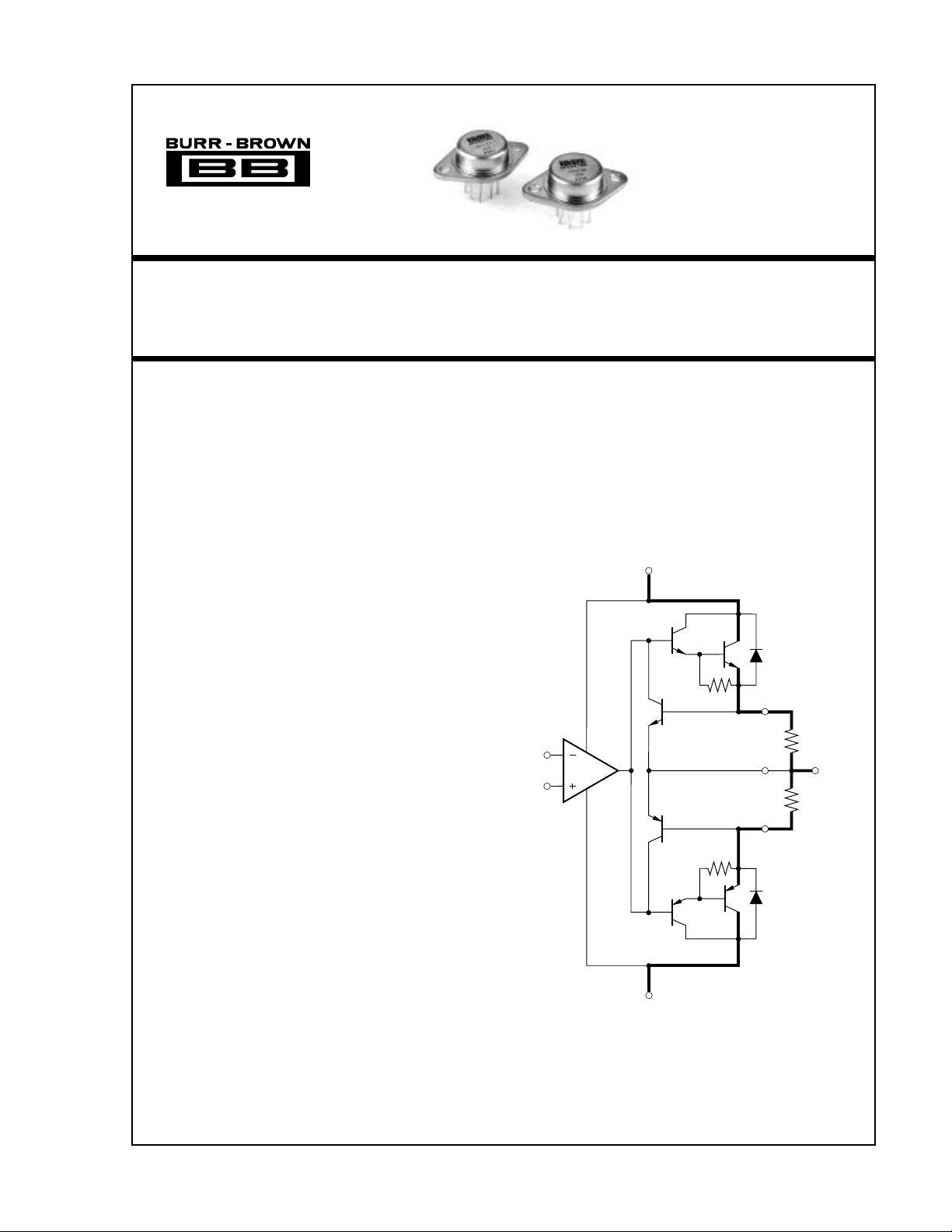
The OPA501 is a high output current operational
amplifier. It can be used in virtually all common op
amp circuits, yet is capable of output currents up to
±10A. Power supply voltages up to ±40V allow very
high output power for driving motors or other electromechanical loads.
Safe operating area is fully specified, and user-set
current limits provide protection for both the amplifier
and load. The class-B (zero output stage bias) provides
low quiescent current during small-signal conditions.
This rugged hybrid integrated circuit is packaged in a
metal 8-pin TO-3 package. Both industrial and military temperature range models are available.
APPLICATIONS
● MOTOR DRIVER
● SERVO AMPLIFIER
● VALVE ACTUATOR
● SYNCRO DRIVER
● PROGRAMMABLE POWER SUPPLY
V+
3
+Output
2
Drive
5
4
1
Current
Sense
8
–Output
Drive
+
R
CL
Output
–
R
CL
6
V–
International Airport Industrial Park • Mailing Address: PO Box 11400 • Tucson, AZ 85734 • Street Address: 6730 S. Tucson Blvd. • Tucson, AZ 85706
Tel: (520) 746-1111 • Twx: 910-952-1111 • Cable: BBRCORP • Telex: 066-6491 • FAX: (520) 889-1510 • Immediate Product Info: (800) 548-6132
©
1983 Burr-Brown Corporation PDS-490F Printed in U.S.A. August, 1993
Page 2
SPECIFICATIONS
ELECTRICAL
At TC = +25°C, VS = ±28V, (OPA501RM, AM); VS = ±34V (OPA501SM, BM) unless otherwise noted.
OPA501RM, AM OPA501SM, BM
PARAMETER CONDITIONS MIN TYP MAX MIN TYP MAX UNITS
RATED OUTPUT
Output Current RL = 2Ω (RM, AM) ±10 * A
Continuous
Output Voltage
DYNAMIC RESPONSE
Bandwidth, Unity Gain Small Signal 1 * MHz
Full Power Bandwidth V
Slew Rate R
INPUT OFFSET VOLTAGE
Initial Offset ±5 ±10 ±2 ±5mV
vs Temperature –25°C < T < +85°C (AM, BM) ±10 ±65 µV/°C
vs Supply Voltage ±35 * µV/V
INPUT BIAS CURRENT
Initial T
vs Temperature ±0.05 * nA/°C
vs Supply Voltage ±0.02 * nA/V
INPUT DIFFERENCE CURRENT
Initial T
vs Temperature –25°C < T < +85°C (AM, BM) ±0.01 nA/°C
OPEN-LOOP GAIN, DC R
R
= 6.5Ω (SM, BM) 98 115 dB
L
INPUT IMPEDANCE
Differential 10 * MΩ
Common-mode 250 * MΩ
INPUT NOISE
Voltage Noise f
f
= 10Hz to 10kHz 5 * µVrms
n
Current Noise f
f
= 10Hz to 10kHz 4.5 * pArms
n
INPUT VOLTAGE RANGE
Common-mode Voltage
Common-mode Rejection f = DC, V
POWER SUPPLY
Rated Voltage ±28 ±34 V
Operating Voltage Range ±10 ±36 * ±40 V
Current, quiescent ±2.6 ±10 * * mA
TEMPERATURE RANGE case
Specification, RM, SM –55 +125 * * °C
AM, BM –25 +85 * * °C
Operating, derated
performance, AM, BM –55 +125 * * °C
Storage –65 +150 * * °C
THERMAL RESISTANCE Steady State
*Specification same as for OPA501RM, AM.
NOTES: (1) Package must be derated based on a junction-to-case thermal resistance of 2.2°C/W or a junction-to-ambient thermal resistance of 30°C/W. (2) Safe
Operating Area and Power Derating Curves must be observed. (3) With ±R
are observed. Output current greater than 10A is not guaranteed. (4) The absolute maximum voltage is 3V less than supply voltage.
(1, 2)
(3)
(3)
RL = 2.6Ω (SM, BM) ±10 * A
IO = 10A peak ±20 ±23 ±26 ±29 V
= 40Vp-p, RL = 8Ω 10 16 * * kHz
O
= 5Ω (RM, AM) 1.35 * V/µs
L
R
= 6.5Ω (SM, BM) 1.35 * v/µs
L
–55°C < T < +125°C (RM, SM) ±10 ±40 µV/°C
= +25°C1540*20nA
CASE
= +25°C ±5 ±10 ±2 ±3nA
CASE
–55°C < T < +125°C (RM, SM) ±0.01 nA/°C
= 5Ω (RM, AM) 94 115 dB
L
= 0.3Hz to 10Hz 3 * µVp-p
n
= 0.3Hz to 10Hz 20 * pAp-p
n
(4)
Linear Operation ±(|VS|–6) ±(|VS|–3) * * V
= ±(|VS|–6) 70 110 80 * dB
CM
θ
JC
= 0. Peak output current is typically greater than 10A if duty cycle and pulse width limitations
SC
2.0 2.2 * * °C/W
The information provided herein is believed to be reliable; however, BURR-BROWN assumes no responsibility for inaccuracies or omissions. BURR-BROWN assumes
no responsibility for the use of this information, and all use of such information shall be entirely at the user’s own risk. Prices and specifications are subject to change
without notice. No patent rights or licenses to any of the circuits described herein are implied or granted to any third party. BURR-BROWN does not authorize or warrant
any BURR-BROWN product for use in life support devices and/or systems.
®
OPA501
2
Page 3

®
ABSOLUTE MAXIMUM RATINGS
Power Supply Voltage (VS) ................................................................ ±40V
Power Dissipation at +25°C
Differential Input Voltage............................................................... ±V
Common-Mode Input Voltage .............................................................. ±V
Operating Temperature Range ....................................... –55°C to +125°C
Storage Temperature Range .......................................... –65°C to +150°C
Lead Temperature (soldering, 10s)................................................ +300°C
Junction Temperature .................................................................... +200°C
Output Short-Circuit Duration
NOTES: (1) At case temperature of +25°C. Derate at 2.2°C/W above case
temperature of +25°C. (2) Average dissipation. (3) Within safe operating
area and with appropriate derating.
(1, 2)
.......................................................... 79W
(3)
................................................ Continuous
–3V
S
ORDERING INFORMATION
MODEL PACKAGE RANGE
OPA501AM 8-Pin Metal TO-3 –25°C to +85°C
OPA501BM 8-Pin Metal TO-3 –25°C to +85°C
OPA501RM 8-Pin Metal TO-3 –55°C to +125°C
OPA501SM 8-Pin Metal TO-3 –55°C to +125°C
TEMPERATURE
PACKAGE INFORMATION
MODEL PACKAGE NUMBER
PACKAGE DRAWING
OPA501AM 8-Pin Metal TO-3 030
OPA501BM 8-Pin Metal TO-3 030
OPA501RM 8-Pin Metal TO-3 030
OPA501SM 8-Pin Metal TO-3 030
NOTE: (1) For detailed drawing and dimension table, please see end of data
sheet, or Appendix D of Burr-Brown IC Data Book.
(1)
CONNECTION DIAGRAM
Top View
S
V+
3
+In
4
5
–In
+Output
Drive
2
1
Current
Sense
8
6
V–
NC
–Output
7
Drive
+
R
SC
V
O
–
R
SC
3
OPA501
Page 4
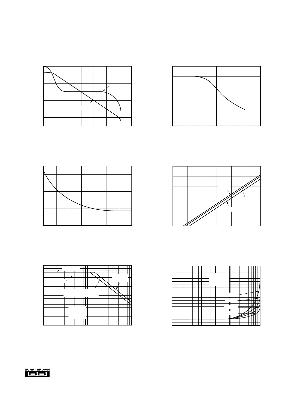
TYPICAL PERFORMANCE CURVES
OUTPUT VOLTAGE SWING
vs POWER SUPPLY VOLTAGE
Power Supply Voltage, V
S
(V)
Output Voltage (Vpk)
±40
±10
±35
±30
±25
±20
±15
±10
±15 ±20 ±25 ±30 ±35 ±40
AV = 10
IO = 1A
IO = 5A
IO = 10A
Typical at +25°C case and ±V
= 28VDC, unless otherwise noted.
S
120
100
80
60
40
Amplitude (dB)
20
0
–20
1
2.8
2.4
2.0
1.6
1.2
OPEN-LOOP FREQUENCY RESPONSE
Phase
Amplitude
10 100 1k 10k 100k 1M 10M
Frequency (Hz)
INPUT BIAS CURRENT vs TEMPERATURE
0
–30
–60
–90
–120
–150
–180
–210
120
100
80
60
Phase (degree)
40
20
Common-Mode Rejection (dB)
0
1
COMMON MODE REJECTION vs FREQUENCY
10 100 1k 10k 100k 1M
Frequency (Hz)
Input Bias Current (Normalized)
Output Voltage Swing (Vp-p)
0.8
0.4
0
–50 –25 0 25 50 75 100 125
Case Temperature (°C)
FULL POWER RESPONSE
100
60
40
+VS = ±34V
+VS = ±28V
Maximum
Output
20
Maximum “Undistorted”
10
Sine Wave Output
6
4
2
RL = 8
A
V =
T
C =
Ω
+10
+25°C
1 2 4 6 10 20 40 60
Frequency (kHz)
®
OPA501
100
HARMONIC DISTORTION vs FREQUENCY
1.8
10
2
VO = 40Vp-p
= +10
A
V
= ±28V
V
S
RL = 16
RL = 50
RL = 4
RL = 8
10
Ω
Ω
Ω
Ω
3
4
10
1.6
1.4
1.2
1.0
0.8
0.6
0.4
Total Harmonic Distortion (%)
0.2
0
10
Frequency (kHz)
4
Page 5

®
TYPICAL PERFORMANCE CURVES (CONT)
NORMALIZED THERMAL RESISTANCE
vs FREQUENCY
Frequency (Hz)
Normalized (
JC
)
1.2
1.0
0.8
0.6
0.4
0.2
0
0.1 1 10 100 1k 10k
θ
Typical at +25°C case and ±V
= 28VDC, unless otherwise noted.
S
120
(W)
100
D
80
60
40
20
Internal Power Dissipation, P
0
0
±7
±6
±5
±4
±3
±2
Short Circuit Current (A)
±1
POWER DERATING CURVE
25 50 75 100 125 150
CURRENT LIMIT vs TEMPERATURE
= 2.2°C/W
θ
JC
Case Temperature (°C)
RSC = 0.12Ω
RSC = 0.28Ω
0.28
0.24
(Ω)
SC
0.20
0.16
0.12
0.08
Current Limit Resistor, R
0.04
CURRENT LIMIT RESISTOR vs LIMIT CURRENT
TC = +25°C
0
02468101214
Limit Current (A)
0
–50 –25 0 25 50 75 100 125
Case Temperature (°C)
PULSE RESPONSE, AV = +1
Input/Output Voltage (5V/div)
Time (10µs/div)
PULSE RESPONSE, AV = +1
Input/Output Voltage (5V/div)
Time (100µs/div)
5
OPA501
Page 6
APPLICATIONS INFORMATION
1 2 4 6 10 20 40 60 80
10
4
2
1.0
0.8
0.6
0.4
0.2
0.1
Output Current (A)
Voltage Across Output Transistor (V)
8
6
100
Maximum
Specified
Current
8
T
CASE
= +25°C
T
JUNCTION
= +200°C
JC
= 2.2°C/W
θ
1ms
0.5ms
Maximum
Specified
Voltage
RM, AM
SM, BM
5ms
DC
Power
Dissipation
Limit
Second
Breakdown
Limit
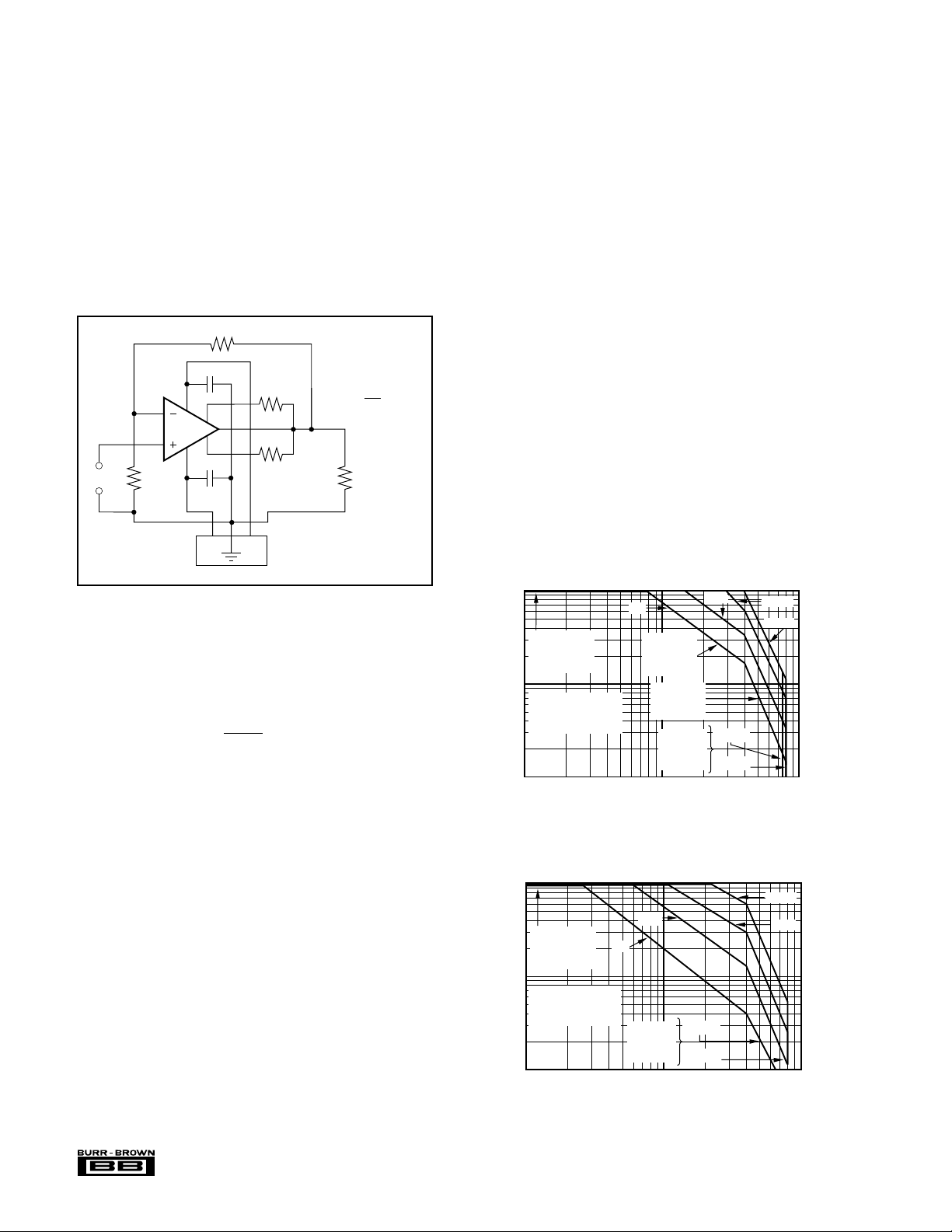
Grounding techniques can greatly affect the performance of
a power op amp. Figure 1 shows grounds connected so that
load current does not flow through signal ground connections. Power supply and load connections should be physically separated from the amplifier input and signal connections.
Power supply connections to the amplifier should be bypassed with 10µF tantalum capacitors connected close to the
device pins. The capacitors should be connected to load
ground as shown.
R
2
(1)
+
OPA501
(1)
V
R
IN
1
+
V– V+
+
R
SC
–
R
SC
G = 1 +
NOTE: (1) 10µF Tantalum.
Load
R
2
R
1
Figure 2, shows the permissible range of voltage and current. SOA is reduced at high operating temperature—see
Figure 3.
The safe output current decreases as V
increases. Output
CE
short-circuits are very demanding. A short-circuit to ground
forces the full power supply voltage (positive or negative
side) across the conducting transistor. With V
current limit must be set for 2A to be safe for short-circuit
= ±30V, the
S
to ground. For further information on SOA and evaluating
signal and load conditions, consult Applications Bulletin
AB-039.
HEAT SINKING
Most applications require a heat sink to assure that the
maximum junction temperature of 200°C is not exceeded.
The size of the heat sink required depends on the power
dissipated by the amplifier and ambient temperature conditions. Application Bulletin AB-039 explains how to find
maximum power dissipation for DC, AC, reactive loads, and
other conditions. Applications Bulletin AB-038 shows how
to determine heat sink requirements.
The case of the OPA501 is isolated from all circuitry and can
be fastened directly to a heat sink. This eliminates cumbersome insulating hardware that degrades thermal performance. See Applications Bulletin AB-037 for information
on mounting techniques and procedures.
FIGURE 1. Basic Circuit Connections.
CURRENT LIMITS
The OPA501 has independent positive and negative current
limit circuits. Current limits are set by the value of R
–
. The approximate value of these resistors is:
R
SC
0.65
RSC=
I
LIMIT
is the desired maximum current at room temperature in
I
LIMIT
Amperes and R
is in ohms. The current limit value de-
SC
creases with increasing temperature—see typical performance curves. The current limit resistors conduct the full
amplifier output current. Power dissipation of the current
limit resistors at maximum current is:
P
= (I
MAX
The current limit resistors can be chosen from a variety of
types. Most wire-wound types are satisfactory, although
some physically large resistors may have excessive inductance which can cause instability.
SAFE OPERATING AREA
Stress on the output transistor is determined by the output
current and the voltage across the conducting output transistor. The power dissipated by the output transistor is equal to
the product of the output current and the voltage across the
conducting transistor, V
®
OPA501
. The Safe Operating Area (SOA),
CE
− 0.0437Ω
)2R
LIMIT
SC
+
and
SC
FIGURE 2. Transistor Safe Operating Area at +25°C Case
Temperature.
10
8
6
4
Maximum
Specified
2
Current
1.0
T
= +125°C
CASE
0.8
0.6
Output Current (A)
0.4
0.2
0.1
1 2 4 6 10 20 40 60 80
T
JUNCTION
θ
= 2.2°C/W
JC
= +200°C
Voltage Across Output Transistor (V)
DC
Maximum
Specified
Voltage
5ms
RM, AM
SM, BM
8
0.5ms
1ms
100
FIGURE 3. Transistor Safe Operating Area at +125°C Case
Temperature.
6
 Loading...