

Page 1
R
l
)
)
SBOS313B − AUGUST 2004 − REVISED NOVEMBER 2004
Please be aware that an important notice concerning availability, standard warranty, and use in critical applications of Texas Instruments
Precision, Low Power, 18MHz
Transimpedance Amplifier
OPA381
OPA2381
FEATURES
D OVER 250kHz TRANSIMPEDANCE
BANDWIDTH
D DYNAMIC RANGE: 5 Decades
D EXCELLENT LONG-TERM STABILITY
D LOW VOLTAGE NOISE: 10nV/√Hz
D BIAS CURRENT: 3pA
D OFFSET VOLTAGE: 25µV (max)
D OFFSET DRIFT: 0.1µV/°C (max)
D GAIN BANDWIDTH: 18MHz
D QUIESCENT CURRENT: 800µA
D FAST OVERLOAD RECOVERY
D SUPPLY RANGE: 2.7V to 5.5V
D SINGLE AND DUAL VERSIONS
D MicroPACKAGE: DFN-8, MSOP-8
APPLICATIONS
D PRECISION I/V CONVERSION
D PHOTODIODE MONITORING
D OPTICAL AMPLIFIERS
D CAT-SCANNER FRONT-END
D PHOTO LAB EQUIPMENT
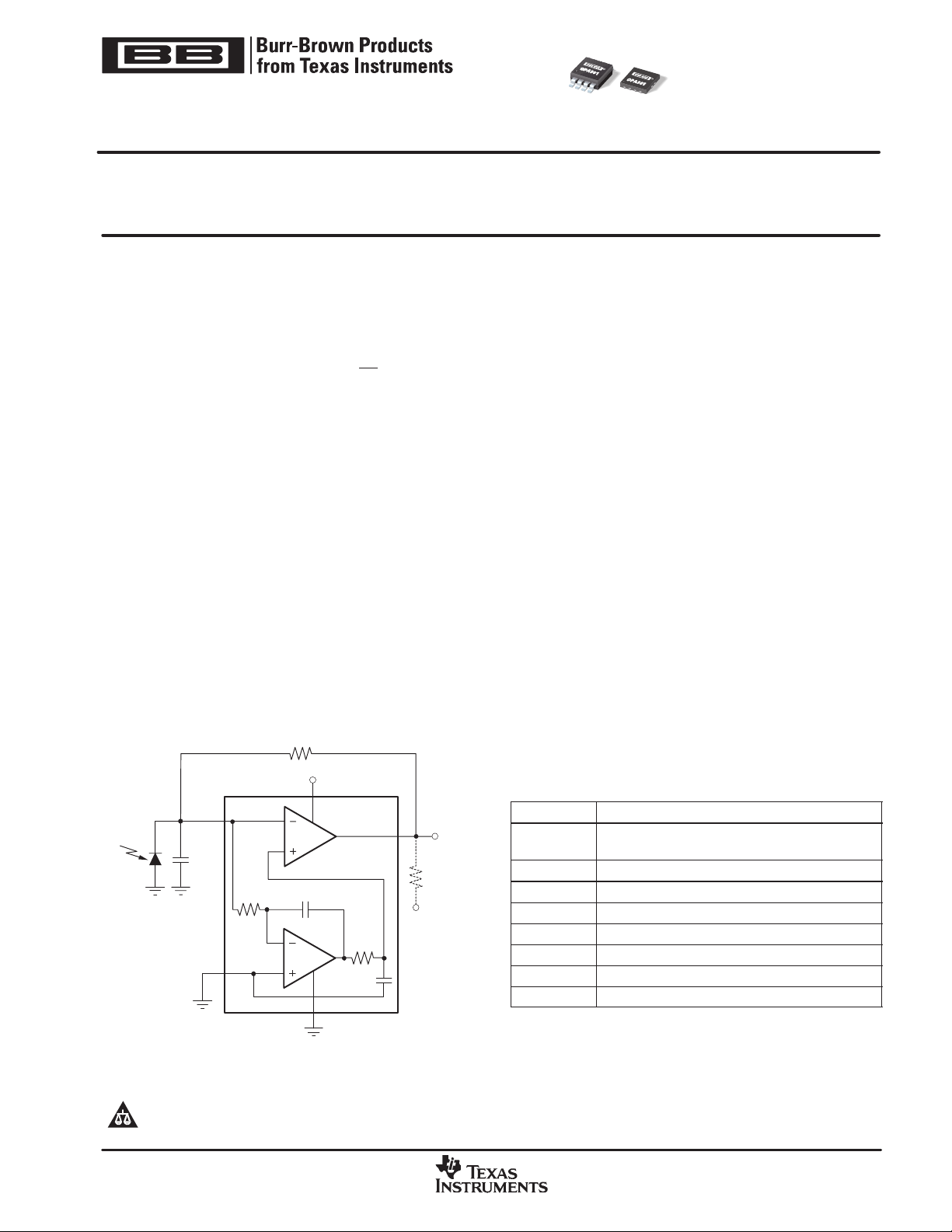
F
+5V
7
65pF
4
OPA381
Ω
100k
75pF
Photodiode
C
DIODE
2
Ω
1M
3
6
−
5V
V
OUT
(0V to 4.4V
R
P
(Optiona
Pulldown
Resistor
DESCRIPTION
The OPA381 family of transimpedance amplifie rs provides
18MHz of Gain Bandwidth (GBW), with extremely high
precision, excellent long-ter m stability, and v er y l ow 1 /f n oise.
The OP A381 features a n o f fset v oltage o f 2 5µV ( max), o f fset
drift of 0.1µV/°C (max), and bias c urrent o f 3pA. The O PA381
far exceeds the offset, drift, and noise performance that
conventional JFET op amps provide.
The signal b andwidth of a t ransimpedance a mplifier d epends
largely on the GBW of the amplifier and the parasitic
capacitance of the photodiode, as well as the feedback
resistor. The 18MHz GBW of the OPA381 enables a transimpedance bandwidth of > 250kHz in mos t configurations.
The OPA381 is ideally suited for fast control loops for power
level measurement on an optical fiber.
As a result o f t he h igh p recision and l ow-noise c haracteristics
of the OPA381, a dynamic range of 5 decades can be
achieved. This capability allows the measurement of signal
currents on the order of 10nA, and up to 1mA in a single I/V
conversion stage. In contrast to logarithmic amplifiers, the
OPA381 provides very wide bandwidth throughout the full
dynamic range. By using an external pulldown resistor to
–5V , t he output voltage r ange c an b e e xtended t o i nclude 0 V.
The OP A381 and OPA2381 are both available in MSOP-8
and DFN-8 (3mm x 3mm) packages. They are specified
from –40°C to +125°C.
OPA381 RELATED DEVICES
PRODUCT FEATURES
OPA380
OPA132 16MHz GBW, Precision FET Op Amp ±15V
OPA300 150MHz GBW, Low-Noise, 2.7V to 5.5V Supply
OPA335 10µV VOS, Zero-Drift, 2.5V to 5V Supply
OPA350 500µV VOS, 38MHz, 2.5V to 5V Supply
OPA354 100MHz GBW CMOS, RRIO, 2.5V to 5V Supply
OPA355 200MHz GBW CMOS, 2.5V to 5V Supply
OPA656/7 230MHz, Precision FET, ±5V
90MHz GBW, 2.7V to 5.5V Supply
Transimpedance Amplifier
semiconductor products and disclaimers thereto appears at the end of this data sheet.
All trademarks are the property of their respective owners.
! !
www.ti.com
Copyright 2004, Texas Instruments Incorporated
Page 2
"#$
OPA381
MSOP-8
DGK
−40°C to +125°C
A64
OPA381
DFN-8
DRB
−40°C to +125°C
A65
OPA2381
MSOP-8
DGK
−40°C to +125°C
A62
OPA2381
DFN-8
DRB
−40°C to +125°C
A63
%"#$
SBOS313B − AUGUST 2004 − REVISED NOVEMBER 2004
www.ti.com
ABSOLUTE MAXIMUM RATINGS
(1)
Voltage Supply +7V. . . . . . . . . . . . . . . . . . . . . . . . . . . . . . . . . . . . . . .
Signal Input Terminals
(2)
,Voltage (V−) −0.5V to (V+) + 0.5V. . . . .
Current ±10mA. . . . . . . . . . . . . . . . . . . . .
Short-Circuit Current
(3)
Continuous. . . . . . . . . . . . . . . . . . . . . . . .
ELECTROSTATIC DISCHARGE SENSITIVITY
This integrated circuit can be damaged by ESD. Texas
Instruments recommends that all integrated circuits be
handled with appropriate precautions. Failure to observe
proper handling and installation procedures can cause damage.
Operating Temperature Range −40°C to +125°C. . . . . . . . . . . . . . .
Storage Temperature Range −65°C to +150°C. . . . . . . . . . . . . . . . .
Junction Temperature +150°C. . . . . . . . . . . . . . . . . . . . . . . . . . . . . . .
Lead Tem perature (soldering, 10s) +300°C. . . . . . . . . . . . . . . . . . . . .
OPA381 ESD Rating (Human Body Model) 2000V. . . . . . . . . . . . . . .
ESD damage can range from subtle performance degradation to
complete device failure. Precision integrated circuits may be more
susceptible t o damage because very small parametric changes could
cause the device not to meet its published specifications.
OPA2381 ESD Rating (Human Body Model) 1500V. . . . . . . . . . . . . .
(1)
Stresses above these ratings may cause permanent damage.
Exposure to absolute maximum conditions for extended periods
may degrade device reliability. These are stress ratings only , an d
functional operation of the device at these or any other conditions
beyond those specified is not implied.
(2)
Input terminals are diode clamped to the power-supply rails. Input
signals that can swing more than 0.5V beyond the supply rails
should be current limited to 10mA or less.
(3)
Short-circuit to ground; one amplifier per package.
PACKAGE/ORDERING INFORMATION
PRODUCT PACKAGE-LEAD
PACKAGE
DESIGNATOR
(1)
SPECIFIED
TEMPERATURE
RANGE
PACKAGE
MARKING
ORDERING
NUMBER
OPA381AIDGKT Tape and Reel, 250
OPA381AIDGKR Tape and Reel, 2500
OPA381AIDRBT T ape and Reel, 250
OPA381AIDRBR T ape and Reel, 3000
OPA2381AIDGKT Tape and Reel, 250
OPA2381AIDGKR Tape and Reel, 2500
OPA2381AIDRBT Tape and Reel, 250
OPA2381AIDRBR T ape and Reel, 3000
(1)
For the most current package and ordering information, see the Package Option Addendum located at the end of this data sheet.
TRANSPORT
MEDIA, QUANTITY
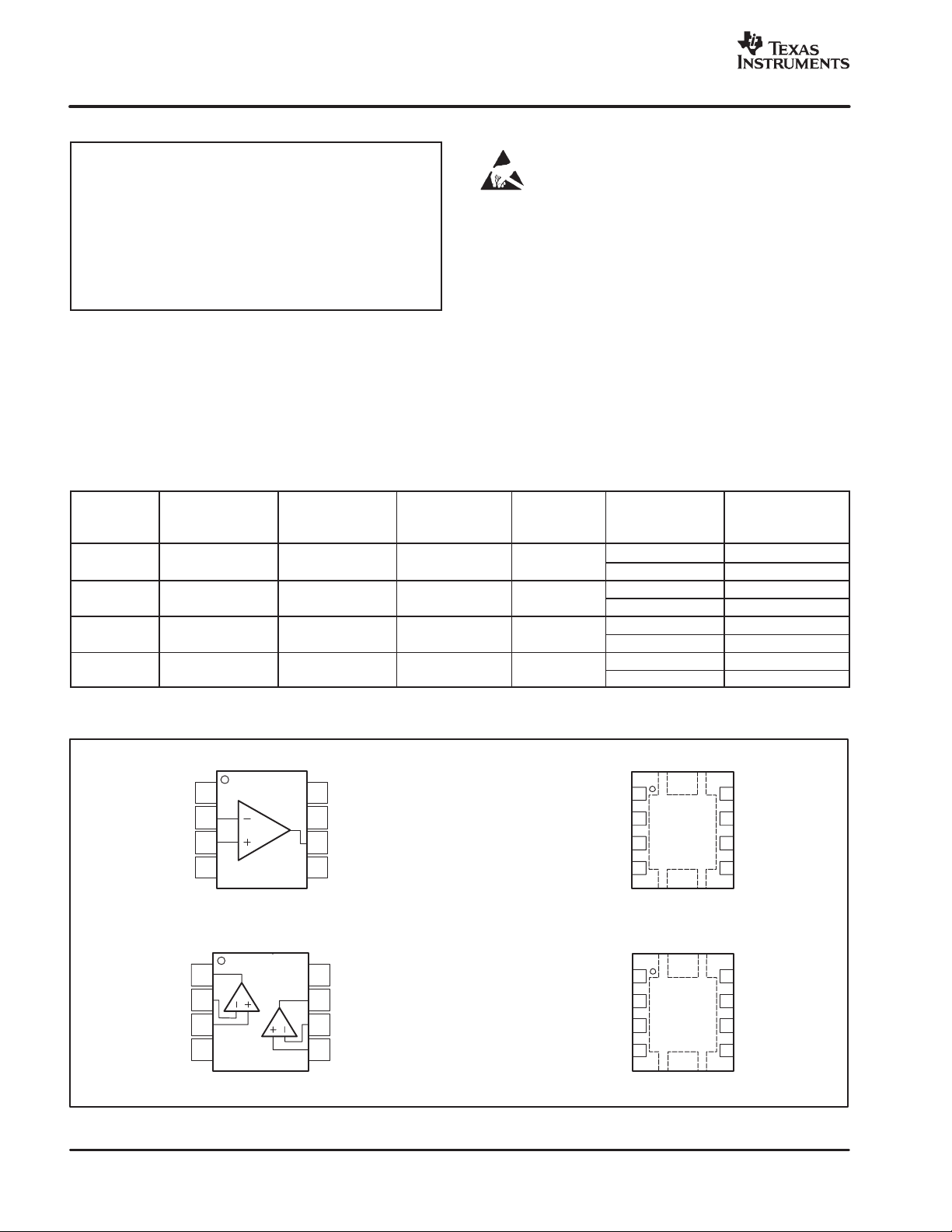
PIN ASSIGNMENTS
Top View
(1)
1
NC
−
In
2
3
+In
−
V
4
Out A
1
−
In A
2
+In A
3
−
V
4
2
OPA381
MSOP−8
OPA2381
MSOP−8
OPA381
(1)
NC
8
V+
7
Out
6
(1)
NC
5
NOTE: (1) NC indicates no internal connection.
V+
8
Out B
7
−
In B
6
+In B
5
NC
−
+In
V
Out A
−
In A
+In A
V
(1)
1
Exposed
Thermal
In
2
Die Pad
3
on
Underside
−
4
DFN−8
OPA2381
1
Exposed
Thermal
2
Die Pad
3
on
Underside
−
4
DFN−8
(1)
NC
8
V+
7
Out
6
(1)
NC
5
V+
8
OutB
7
−
In B
6
+In B
5
Page 3

"#$
%"#$
www.ti.com
SBOS313B − AUGUST 2004 − REVISED NOVEMBER 2004
ELECTRICAL CHARACTERISTICS: VS = +2.7V to +5.5V
Boldface limits apply over the temperature range, TA = −40°C to +125°C.
All specifications at TA = +25°C, RL = 10kΩ connected to VS/2, and V
PARAMETER CONDITION
OFFSET VOLTAGE
Input Offset Voltage V
Drift dVOS/dT 0.03 0.1 µV/°C
vs Power Supply PSRR VS = +2.7V to +5.5V, VCM = 0V 3.5 20 µV/V
Over Temperature VS = +2.7V to +5.5V, VCM = 0V 20 µV/V
Long-Term Stability
Channel Separation, dc 1 µV/V
INPUT BIAS CURRENT
Input Bias Current I
Over Temperature See Typical Characteristics
Input Offset Current I
NOISE
Input Voltage Noise, f = 0.1Hz to 10Hz e
Input Voltage Noise Density, f = 10kHz e
Input Voltage Noise Density, f > 1MHz e
Input Current Noise Density, f = 10kHz i
INPUT VOLTAGE RANGE
Common-Mode Voltage Range V
Common-Mode Rejection Ratio CMRR VS = +5V, (V−) < VCM < (V+) − 1.8V 95 110 dB
INPUT IMPEDANCE
Differential Capacitance 1 pF
Common-Mode Resistance and Capacitance 1013|| 2.5 Ω || pF
OPEN-LOOP GAIN
Open-Loop Voltage Gain A
FREQUENCY RESPONSE
Gain-Bandwidth Product GBW 18 MHz
Slew Rate SR G = +1 12 V/µs
Settling Time, 0.0015%
Settling Time, 0.003%
Overload Recovery Time
OUTPUT
Voltage Output Swing from Positive Rail RL = 10kΩ 400 600 mV
Voltage Output Swing from Negativ e Ra il RL = 10kΩ 30 50 mV
Voltage Output Swing from Positive Rail RP = 10kΩ to −5V
Voltage Output Swing from Negativ e Ra il RP = 10kΩ to −5V
Output Current I
Short-Circuit Current I
Capacitive Load Drive C
Open-Loop Output Impedance R
POWER SUPPL Y
Specified Voltage Range V
Quiescent Current (per amplifier) I
Over Temperature 1.1 mA
TEMPERATURE RANGE
Specified and Operating Range −40 +125 °C
Storage Range −65 +150 °C
Thermal Resistance q
MSOP-8 150 °C/W
DFN-8 65 °C/W
(1)
High temperature operating life characterization of zero-drift op amps applying the techniques used in the OPA381 have repeatedly demonstrated randomly
distributed variation approximately equal to measurement repeatability of 1µV. This consistency gives confidence in the stability and repeatability of these zerodrift techniques.
(2)
Tested with output connected only to RP, a pulldown resistor connected between V
Output Swing to Negative Rail.
(3)
Transimpedance frequency of 250kHz.
(4)
Time required to return to linear operation.
(5)
From positive rail.
(1)
(3)
(3)
(4), (5)
OS
OS
CM
OL
OUT
SC
LOAD
B
n
n
n
n
0.05V < VO < (V+) − 0.6V, VCM = VS/2, VS = 5V 110 135 dB
0V < V
< (V+) − 0.6V, V
O
VS = +5V, 4V Step, G = +1, OPA381 7 µs
VS = +5V, 4V Step, G = +1, OPA2381 7 µs
O
S
Q
JA
= VS/2, unless otherwise noted.
OUT
MIN TYP MAX
VS = +5V, VCM = 0V 7 25 µV
VCM = VS/2 3 ±50 pA
VCM = VS/2 6 ±100 pA
VS = +5V, VCM = 0V 3 µV
VS = +5V, VCM = 0V 70 nV/√Hz
VS = +5V, VCM = 0V 10 nV/√Hz
VS = +5V, VCM = 0V 20 fA/√Hz
V− (V+) − 1.8V V
= 0V, R
CM
VIN • G = > V
F = 1MHz, IO = 0 250 Ω
= 10kΩ to −5V
P
S
(2)
(2)
IO = 0A 0.8 1 mA
and −5V , as shown in Figure 3. See also Applications section, Achieving
OUT
(2)
, VS = 5V 106 135 dB
2.7 5.5 V
OPA381
UNITS
See Note (1)
200 ns
400 600 mV
−20 0 mV
10 mA
20 mA
See Typical Characteristics
PP
3
Page 4
"#$
%"#$
SBOS313B − AUGUST 2004 − REVISED NOVEMBER 2004
TYPICAL CHARACTERISTICS: VS = +2.7V to +5.5V
All specifications at TA = +25°C, RL = 10kΩ connected to VS/2, and V
= VS/2, unless otherwise noted.
OUT
www.ti.com
140
OPEN−LOOPGAIN AND PHASE vsFREQUENCY
120
Phase
100
80
60
40
20
Open−Loop Gain(dB)
Gain
0
−
20
10 100k 1M100 1k 10k 100M10M
Frequency (Hz)
PHASE MARGIN vs LOAD CAPACITANCE
90
80
70
)
_
60
50
40
Phase Margin(
30
RS=50
Ω
RS=0
20
10
0 100 200 300 400 500 600 700 900800 1000
Load Capacitance (pF)
C
L
RS=100
Ω
100pF
POWER−SUPPLY REJECTION RATIO AND
200
150
100
50
0
−
−
−
−
50
100
150
200
140
120
100
)
_
Phase (
PSRR, CMRR (dB)
−
−
−
COMMON−MODE REJECTION vs FREQUENCY
80
PSRR
60
40
20
0
CMRR
20
40
60
10 100k 1M100 1k 10k 100M10M
Frequency (Hz)
QUIESCENT CURRENT vs TEMPERATURE
Ω
1.00
0.90
0.85
Ω
50k
R
S
C
L
0.80
5.5V
0.75
0.70
0.65
2.7V
Quiescent Current (mA)
0.60
0.55
0.50
−
−
40 100 125
25 0 25 50 75
Temperature (_C)
1.00
QUIESCENT CURRENT vs SUPPLY VOLTAGE
1000
INPUT BIAS CURRENT vs TEMPERATURE
0.90
0.85
0.80
100
0.75
0.70
0.65
Quiescent Current (mA)
0.60
10
Input BiasCurrent (pA)
0.55
0.50
2.73.13.53.94.34.75.15.5
Supply Voltage (V)
1
−
−
40 100 125
25 0 25 50 75
Temperature (_C)
4
Page 5
www.ti.com
OUTPUT VOLTAGE SWING vs OUTPUT CURRENT
OFFSETVOLTAGE DRIFT
GAIN BANDWIDTH vs POWER SUPPLY VOLTAGE
SBOS313B − AUGUST 2004 − REVISED NOVEMBER 2004
TYPICAL CHARACTERISTICS: VS = +2.7V to +5.5V (continued)
All specifications at TA = +25°C, RL = 10kΩ connected to VS/2, and V
= VS/2, unless otherwise noted.
OUT
"#$
%"#$
Input BiasCurrent (pA)
(V+)−0.35
(V+)−0.70
(V+)−1.05
(V+)−1.40
(V−) + 1.40
Output Swing (V)
(V−) + 1.05
(V−) + 0.70
(V−) + 0.35
INPUT BIAS CURRENT
50
40
30
20
10
0
−
10
−
20
−
30
−
40
−
50
0 0.5 1.0 1.5 2.0 2.5 3.0 3.5
(V+)
(V−)
vs COMMON−MODE VOLTAGE
−
I
B
+
I
B
Common−Mode Voltage (V)
(VS=2.7V)
+125_C
+25_C
5 101520250
Output Current (mA)
−40_
C
(V+)−1
(V+)−2
(V−)+2
OutputSwing (V)
(V−)+1
OUTPUT VOLTAGE SWING vs OUTPUT CURRENT
(V+)
(V−)
Population
0.10−0.09−0.08−0.07−0.06−0.05−0.04−0.03−0.02−0.01
−
=5.5V)
(V
S
+125_C
5101520250
Output Current (mA)
PRODUCTION DISTRIBUTION
0.00
0.01
0.02
0.03
Offset Voltage Drift (µV/_C)
0.04
+25°C
−40_
0.05
0.06
C
0.07
0.08
0.09
0.10
OFFSET VOLTAGE PRODUCTION DISTRIBUTION
Population
25.00−20.00−15.00−10.00
−
5.00
0.00
−
Offset Voltage (µV)
20
19
18
17
16
15
14
GainBandwidth (MHz)
13
12
5.00
10.00
15.00
20.00
25.00
3.5 4.03.0 4.5 5.0 5.52.5
Power Supply Voltage (V)
5
Page 6
"#$
%"#$
SBOS313B − AUGUST 2004 − REVISED NOVEMBER 2004
TYPICAL CHARACTERISTICS: VS = +2.7V to +5.5V (continued)
All specifications at TA = +25°C, RL = 10kΩ connected to VS/2, and V
= VS/2, unless otherwise noted.
OUT
www.ti.com
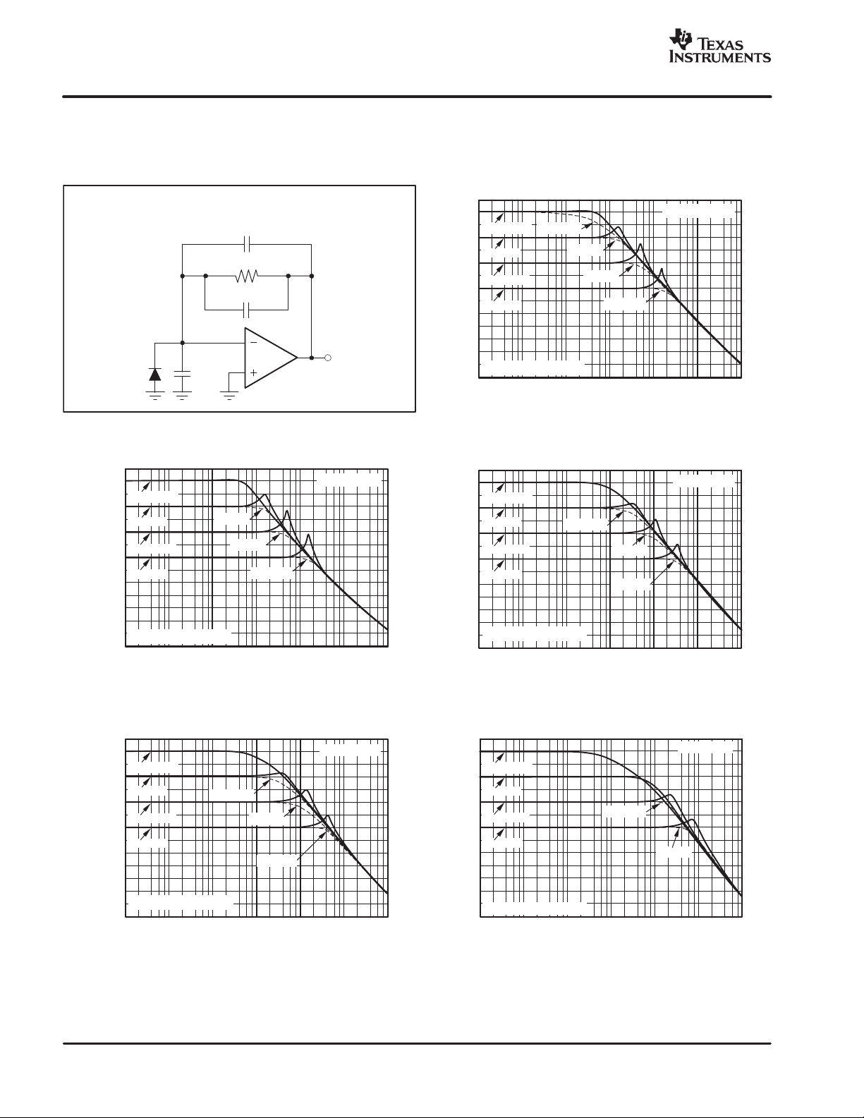
Circuit for Transimpedance Amplifier Characteristic curves on this page.
C
F
R
F
C
STRAY
OPA381
C
DIODE
TRANSIMPEDANCE AMPCHARACTERISTIC
150
140
130
120
110
RF=10MΩ
RF=1M
Ω
CF=1pF
C
DIODE
= 50pF
100
90
80
70
60
RF= 100kΩ
RF=10kΩ
CF= 3pF
CF=8pF
50
40
30
Transimpedance Gain (V/A in dB)
20
C
(parasitic) = 0.2pF
STRAY
10
100
1k 10k 100k 1M 10M 100M
Frequency (Hz)
150
140
130
120
110
RF=10MΩ
RF=1M
Ω
CF= 0.5pF
CF=1pF
C
DIODE
100
TRANSIMPEDANCE AMPCHARACTERISTIC
90
80
70
60
RF= 100kΩ
RF=10kΩ
CF= 4pF
CF=12pF
50
40
30
Transimpedance Gain (V/A in dB)
20
C
(parasitic) = 0.2pF
STRAY
10
100
1k 10k 100k 1M 10M 100M
Frequency (Hz)
TRANSIMPEDANCE AMPCHARACTERISTIC
150
140
130
RF= 10M
Ω
C
DIODE
120
110
100
90
80
70
60
RF=100k
RF= 10k
Ω
Ω
CF=0.5pF
CF=2pF
CF=5pF
Ω
RF=1M
50
40
30
Transimpedance Gain (V/A in dB)
C
(parasitic) = 0.2pF
STRAY
20
10
100 1k 10k 100k 1M 10M 100M
Frequency (Hz)
= 100pF
= 20pF
150
140
130
RF= 10M
Ω
C
DIODE
120
TRANSIMPEDANCE AMPCHARACTERISTIC
110
100
90
80
70
60
50
RF=100k
RF= 10k
Ω
Ω
CF=0.5pF
CF=2pF
CF=4pF
Ω
RF=1M
40
30
Transimpedance Gain (V/A in dB)
C
(parasitic) = 0.2pF
STRAY
20
10
100 1k 10k 100k 1M 10M 100M
Frequency (Hz)
= 10pF
150
140
130
120
110
100
90
80
70
60
50
40
30
Transimpedance Gain (V/A in dB)
20
10
TRANSIMPEDANCE AMP CHARACTERISTIC
C
=1pF
DIODE
Ω
RF= 10M
Ω
RF=1M
RF=100k
RF= 10k
C
STRAY
Ω
Ω
(parasitic) = 0.2pF
CF= 0.5pF
CF= 2pF
100 1k 10k 100k 1M 10M 100M
Frequency (Hz)
6
Page 7
www.ti.com
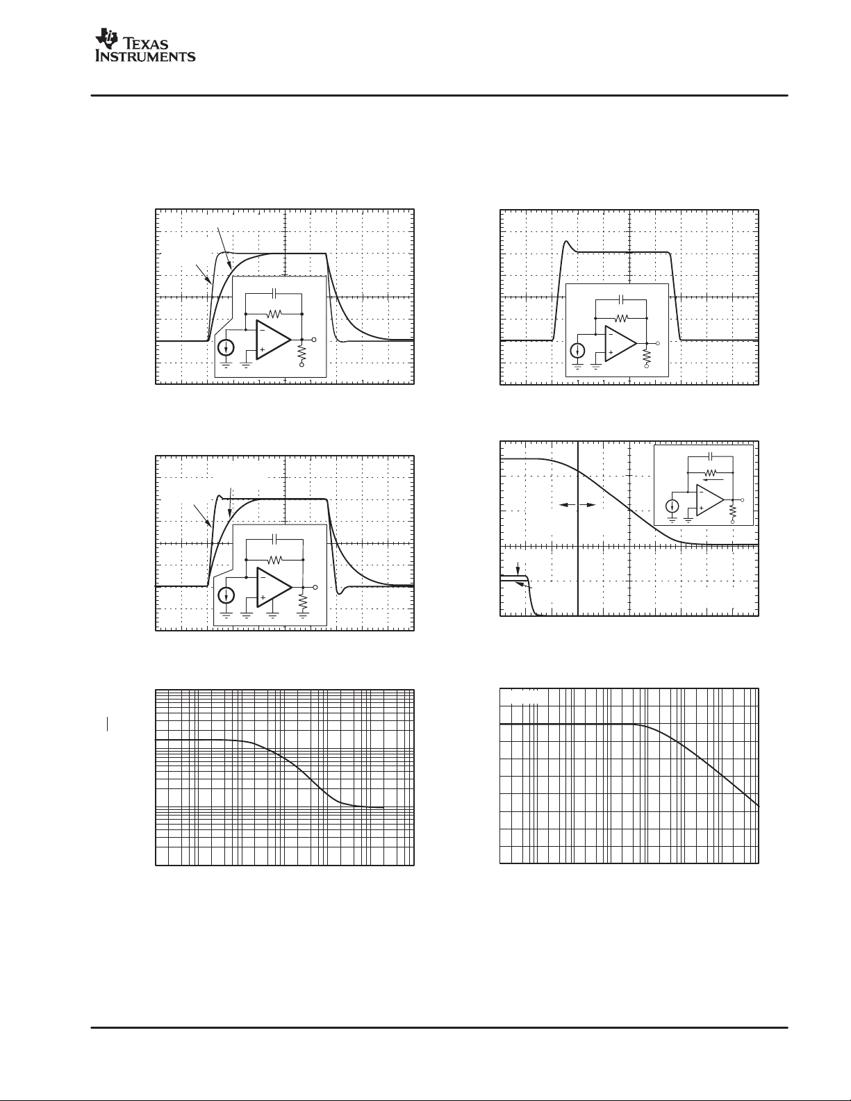
OVERLOAD RECOVERY
SBOS313B − AUGUST 2004 − REVISED NOVEMBER 2004
TYPICAL CHARACTERISTICS: VS = +2.7V to +5.5V (continued)
All specifications at TA = +25°C, and RL = 10kΩ connected to VS/2, unless otherwise noted.
"#$
%"#$
SMALL−SIGNAL STEP RESPONSE
(with or without pull−down)
LARGE−SIGNAL STEP RESPONSE
(with pull−down)
200kHz (CF= 16pF)
1MHz
= 3pF)
(C
F
C
F
Ω
50mV/div
50k
OPA381
Ω
10k
V
P
VP=0Vor−5V
1V/div
Time (100ns/div)
LARGE−SIGNAL STEP RESPONSE
(withoutpull−down)
200kHz
=16pF)
(C
=3pF)
F
C
F
Ω
50k
OPA381
Ω
10k
1MHz
(C
F
1V/div
6
V
OUT
4
(V/div)I
2
OUT
V
0
0.8
(mA/div)
0
IN
Nonlinear
Operation
OPA381
OPA2381
I
IN
0 100 200 300 400 500 600 700 800 900 1000
Time(100ns/div)
3pF
Ω
50k
OPA381
Time (100ns/div)
Linear
Operation
Time (ns)
−5V
10kΩ
I
IN
40pF
20kΩ
250µA
OPA381
10kΩ
V
VP=0Vor−5V
P
1000
INPUT VOLTAGE NOISE SPECTRAL DENSITY
(Hz)
√
100
10
Input Voltage Noise(nV/
1
10 100 100k 1M10k1k 10M
Frequency (Hz)
160
140
CHANNEL SEPARATION vs INPUT FREQUENCY
OPA2381
120
100
80
60
40
20
Channel Separation (dB)
0
−
20
−
40
10 100 1k 10k 100k 1M 10M 100M
Input Frequency (Hz)
7
Page 8

"#$
%"#$
SBOS313B − AUGUST 2004 − REVISED NOVEMBER 2004
www.ti.com
APPLICATIONS INFORMATION
BASIC OPERATION
The OPA381 is a high-precision transimpedance
amplifier with very low 1/f noise. Due to its unique
architecture, the OP A381 has excellent long-term input
voltage offset stability.
The OPA381 performance results from an internal
auto-zero amplifier combined with a high-speed
amplifier. The OPA381 has been designed with circuitry
to improve overload recovery and settling time over that
achieved by a traditional composite approach. It has
been specifically designed and characterized to
accommodate circuit options to allow 0V output
operation (see Figure 3).
The OP A381 is used in inverting configurations, with t h e
noninverting input used as a fixed biasing point.
Figure 1 shows the OPA381 in a typical configuration.
Power-supply pins should be bypassed with 1µF
ceramic or tantalum capacitors. Electrolytic capacitors
are not recommended.
C
F
R
F
+5V
1µF
λ
OPA381
(1)
V
OUT
(0.5V to 4.4V)
OPERATING VOLTAGE
OPA381 series op amps are fully specified from 2.7V to
5.5V over a temperature range of −40°C to +125°C.
Parameters that vary significantly with operating
voltages or temperature are shown in the Typical
Characteristics.
INTERNAL OFFSET CORRECTION
The OPA381 series op amps use an auto-zero topology
with a time-continuous 18MHz op amp in the signal
path. This amplifier is zero-corrected every 100µs using
a proprietary technique. Upon power-up, the amplifier
requires approximately 400µs to achieve specified V
OS
accuracy, which includes one full auto-zero cycle of
approximately 100µs and the start-up time for the bias
circuitry. Prior to this time, the amplifier will function
properly but with unspecified offset voltage.
This design has virtually no aliasing and low noise. Zero
correction occurs at a 10kHz rate, but there is virtually
no fundamental noise energy present at that frequency
due to internal filtering. For all practical purposes, any
glitches have energy at 20MHz or higher and are easily
filtered, if necessary. Most applications are not sensitive
to such high-frequency noise, and no filtering is
required.
INPUT VOLTAGE
The input common-mode voltage range of the OPA381
series extends from V− to (V+) –1.8V. With input signals
above this common-mode range, the amplifier will no
longer provide a valid output value, but it will not latch
or invert.
V
=0.5V
BIAS
NOTE: (1) V
= 0.5V in dark conditions.
OUT
Figure 1. OPA381 Typical Configuration
8
INPUT OVERVOLTAGE PROTECTION
Device inputs are protected by ESD diodes that will
conduct if the input voltages exceed the power supplies
by more than approximately 500mV. Momentary
voltages greater than 500mV beyond the power supply
can be tolerated if the current is limited to 10mA. The
OPA381 family features no phase inversion when the
inputs extend beyond supplies if the input is current
limited.
Page 9

www.ti.com
"#$
%"#$
SBOS313B − AUGUST 2004 − REVISED NOVEMBER 2004
OUTPUT RANGE
The OPA381 is specified to swing within at least 600mV
of the positive rail and 50mV of the negative rail with a
10kΩ load while maintaining good linearity . Swing to the
negative rail while maintaining linearity can be extended
to 0V—see the section, Achieving Output Swing to
Ground. See the Typical Characteristic curve, Output
Voltage Swing vs Output Current.
The OPA381 can swing slightly closer than specified to
the positive rail; however, linearity will decrease and a
high-speed overload recovery clamp limits the amount
of positive output voltage swing available—see
Figure 2.
25
VS=5.5V
20
15
10
5
V)
µ
(
0
OS
V
−
5
−
10
−
15
−
20
−
25
−
10123456
V
OUT
(V)
RP=10kΩto−5V
= 10kΩto VS/2
R
L
Figure 2. Effect of High-Speed Overload
Recovery Clamp on Output Voltage
OVERLOAD RECOVERY
ACHIEVING OUTPUT SWING TO GROUND
Some applications require output voltage swing from
0V to a positive full-scale voltage (such as +4.096V)
with excellent accuracy. With most single-supply op
amps, problems arise when the output signal
approaches 0V, near the lower output swing limit of a
single-supply op amp. A good single-supply op amp
may swing close to single-supply ground, but will not
reach 0V.
The output of the OPA381 can be made to swing to 0V,
or slightly below, on a single-supply power source. This
extended output swing requires the use of another
resistor and an additional negative power supply. A
pulldown resistor may be connected between the
output and the negative supply to pull the output down
to 0V; see Figure 3.
R
F
λ
−
RP=
500µA
Figure 3. Amplifier with Pull-Down Resistor to
Achieve V
V+=+5V
OPA381 V
V−=Gnd
V
S
−
V
S
Negative Supply
= 0V
OUT
RP=10k
=−5V
OUT
Ω
The OPA381 has been designed to prevent output
saturation. After being overdriven to the positive rail, it
will typically require only 200ns to return to linear
operation. The time required for negative overload
recovery is greater, unless a pulldown resistor
connected to a more negative supply is used to extend
the output swing all the way to the negative rail—see the
following section, Achieving Output Swing to Ground.
The OPA381 has an output stage that allows the output
voltage to be pulled to its negative supply rail using this
technique. However, this technique only works with
some types of output stages. The OPA381 has been
designed to perform well with this method. Accuracy is
excellent down to 0V. Reliable operation is assured over
the specified temperature range.
9
Page 10

"#$
%"#$
SBOS313B − AUGUST 2004 − REVISED NOVEMBER 2004
www.ti.com
BIASING PHOTODIODES IN SINGLE-SUPPLY
CIRCUITS
The +IN input can be biased with a positive DC voltage
to offset the output voltage and allow the amplifier
output to indicate a true zero photodiode measurement
when the photodiode is not exposed to any light. It will
also prevent the added delay that results from coming
out of the negative rail. This bias voltage appears
across the photodiode, providing a reverse bias for
faster operation. An RC filter placed at this bias point will
reduce noise. (Refer to Figure 4.) This bias voltage can
also serve as an offset bias point for an ADC with range
that does not include ground.
(1)
C
F
< 1pF
R
F
Ω
10M
V+
λ
I
D
0.1µF
100k
OPA381
Ω
V
OUT=IDRF+VBIAS
D the desired transimpedance gain (R
);
F
D the Gain Bandwidth Product (GBW) for the
OPA381 (18MHz).
With these three variables set, the feedback capacitor
value (CF) can be set to control the frequency response.
C
a typical surface-mount resistor.
To achieve a maximally flat 2nd-order Butterworth
frequency response, the feedback pole should be set
to:
2pR
Bandwidth is calculated by:
f
*3dB
These equations will result in maximum
transimpedance bandwidth. For even higher
transimpedance bandwidth, the high-speed CMOS
OPA380 (90MHz GBW), the OPA300 (150MHz GBW),
or the OPA656 (230MHz GBW) may be used.
For additional information, refer to Application Bulletin
AB−050 (SBOA055), Compensate Transimpedance
Amplifiers Intuitively, available for download at
www.ti.com.
is the stray capacitance of RF, which is 0.2pF for
STRAY
ǒ
CF) C
F
+
1
Ǹ
STRAY
GBW
2pRFC
Ǔ
+
TOT
Ǹ
Hz
GBW
4pRFC
TOT
(1)
(2)
+V
BIAS
[0V to (V+)−1.8V]
NOTE: (1) C
It includes the stray capacitance of R
is optional to prevent gain peaking.
F
.
F
Figure 4. Photodiode with Filtered Reverse Bias
Voltage
TRANSIMPEDANCE AMPLIFIER
Wide bandwidth, low input bias current and low input
voltage and current noise make the OPA381 an ideal
wideband photodiode transimpedance amplifier. Low
voltage noise is important because photodiode
capacitance causes the effective noise gain of the
circuit to increase at high frequency.
The key elements to a transimpedance design are
shown in Figure 5:
D the total input capacitance (C
photodiode capacitance (C
common-mode and differential-mode input
capacitance (2.5pF + 1pF for the OPA381);
), consisting of the
TOT
) plus the parasitic
DIODE
(1)
C
F
R
F
Ω
10M
(2)
C
STRAY
+5V
λ
NOTE: (1) C
(2) C
(3) C
is optionalto prevent gain peaking.
F
STRAY
(typically, 0.2pF for a surface−mount resistor).
TOT
input capacitance.
(3)
OPA381 V
C
TOT
is thestray capacitanceof R
is thephotodiode capacitanceplus OPA381
Figure 5. Transimpedance Amplifier
−
5V
F
OUT
R
(optional
P
pulldownresistor)
10
Page 11

www.ti.com
TRANSIMPEDANCE BANDWIDTH AND
NOISE
Limiting the gain set by RF can decrease the noise
occurring at the output of the transimpedance circuit.
However, all required gain should occur in the
transimpedance stage, since adding gain after the
transimpedance amplifier generally produces poorer
noise performance. The noise spectral density
produced by RF increases with the square-root of RF,
whereas the signal increases linearly. Therefore,
signal-to-noise ratio is improved when all the required
gain is placed in the transimpedance stage.
Total noise increases with increased bandwidth. Limit
the circuit bandwidth to only that required. Use a
capacitor, CF, across the feedback resistor, RF, to limit
bandwidth (even if not required for stability), if total
output noise is a concern.
Figure 6a shows the transimpedance circuit without any
feedback capacitor. The resulting transimpedance gain
of this circuit is shown in Figure 7. The –3dB point is
approximately 3MHz. Adding a 16pF feedback
capacitor (Figure 6b) will limit the bandwidth and result
in a –3dB point at approximately 200kHz (seen in
Figure 7). Output noise will be further reduced by
adding a filter (R
FILTER
pole (Figure 6c). This second pole is placed within the
feedback loop to maintain the amplifier’s low output
impedance. (If the pole was placed outside the
feedback loop, an additional buffer would be required
and would inadvertently increase noise and dc error).
Using R
to represent the equivalent diode
DIODE
resistance, and C
plus OPA381 input capacitance, the noise zero, fZ, is
calculated by:
ǒ
R
f
+
Z
2pR
DIODE
DIODE
R
and C
FILTER
for equivalent diode capacitance
TOT
Ǔ
) R
F
ǒ
C
) C
F
TOT
F
) to create a second
Ǔ
(3)
(c)
λ
"#$
%"#$
SBOS313B − AUGUST 2004 − REVISED NOVEMBER 2004
V
BIAS
V
BIAS
C
RF = 50kΩ
C
STRAY
OPA381
RF = 50kΩ
C
STRAY
CF= 16pF
OPA381
RF = 50kΩ
=0.2pF
STRAY
CF = 22pF
OPA381
=0.2pF
=0.2pF
R
FILTER
= 102kΩ
V
V
C
= 3.9nF
(a)
λ
(b)
λ
V
BIAS
OUT
OUT
V
OUT
FILTER
Figure 6. Transimpedance Circuit Configurations
with Varying Total and Integrated Noise Gain
11
Page 12

"#$
%"#$
SBOS313B − AUGUST 2004 − REVISED NOVEMBER 2004
www.ti.com
120
100
80
60
40
20
Transimpedance Gain (dB)
0
−
20
100 10k1k 1M 10M100k 100M
C
DIODE
= 10pF
SeeFigure6a
−
3dB at 200kHz
SeeFigure6c
Frequency (Hz)
SeeFigure6b
Figure 7. Transimpedance Gains for Circuits in
Figure 6
The effects of these circuit configurations on output
noise are shown in Figure 8 and on integrated output
noise in Figure 9. A 2-pole Butterworth filter (maximally
flat in passband) is created by selecting the filter values
using the equation:
CFRF+ 2C
FILTERRFILTER
(4)
500
C
= 10pF
DIODE
400
Vrms)
µ
300
200
100
Integrated Output Noise (
0
100 10k1k 1M 10M100k 100M
SeeFigure6a
SeeFigure6b
See Figure 6c
Frequency (Hz)
310µVrms
68µVrms
25µVrms
Figure 9. Integrated Output Noise for Circuits in
Figure 6
Figure 10 shows the effects of diode capacitance on
integrated output noise, using the circuit in Figure 6c.
For additional information, refer to Noise Analysis of
FET Transimpedance Amplifiers (SBOA060), and
Noise Analysis for High Speed Op Amps (SBOA066),
available for download from the TI web site.
The circuit in Figure 6b rolls off at 20dB/decade. The
circuit with the additional filter shown in Figure 6c rolls
off at 40dB/decade, resulting in improved noise
performance.
400
C
= 10pF
DIODE
300
Hz)
√
V/
µ
200
100
Output Noise (
0
See Figure 6c
100 1k 10k 1M 10M100k 100M
SeeFigure6a
SeeFigure6b
Frequency (Hz)
Figure 8. Output Noise for Circuits in Figure 6
60
50
Vrms)
µ
40
30
20
See Figure 6c
10
Integrated Output Noise (
0
1 10010 10k1k 1M 10M100k 100M
C
DIODE
= 100pF
C
DIODE
= 20pF
C
DIODE
= 10pF
Frequency (Hz)
C
DIODE
=50pF
C
DIODE
=1pF
56µVrms
37µVrms
28µVrms
25µVrms
23µVrms
Figure 10. Integrated Output Noise for Various
Values of C
for Circuit in Figure 6c
DIODE
12
Page 13

www.ti.com
"#$
%"#$
SBOS313B − AUGUST 2004 − REVISED NOVEMBER 2004
BOARD LAYOUT
Minimize photodiode capacitance and stray
capacitance at the summing junction (inverting input).
This capacitance causes the voltage noise of the op
amp to be amplified (increasing amplification at high
frequency). Using a low-noise voltage source to
reverse-bias a photodiode can significantly reduce its
capacitance. Smaller photodiodes have lower
capacitance. Use optics to concentrate light on a small
photodiode.
Circuit board leakage can degrade the performance of
an otherwise well-designed amplifier. Clean the circuit
board carefully. A circuit board guard trace that
encircles the summing junction and is driven at the
same voltage can help control leakage. See Figure 11.
R
F
λ
OPA381
Guard ri ng
V
OUT
CAPACITIVE LOAD AND STABILITY
The OPA381 series op amps can drive greater than
100pF pure capacitive load. Increasing the gain
enhances the amplifier’s ability to drive greater
capacitive loads. See the Phase Margin vs Load
Capacitance typical characteristic curve.
One method of improving capacitive load drive in the
unity-gain configuration is to insert a 10Ω to 20Ω
resistor inside the feedback loop, as shown in
Figure 12. This reduces ringing with large capacitive
loads while maintaining DC accuracy.
R
F
(3)
C
F
V+
R
S
Ω
V−
20
C
L
V
PD
V
OUT
R
L
(2)
λ
V
OPA381
(1)
B
Figure 11. Connection of Input Guard
OTHER WAYS TO MEASURE SMALL
CURRENTS
Logarithmic amplifiers are used to compress extremely
wide dynamic range input currents to a much narrower
range. Wide input dynamic ranges of 8 decades, or
100pA to 10mA, can be accommodated for input to a
12-bit ADC. (Suggested products: LOG101, LOG102,
LOG104, LOG112.)
Extremely small currents can be accurately measured
by integrating currents on a capacitor. (Suggested
product: IVC102.)
Low-level currents can be converted to high-resolution
data words. (Suggested product: DDC112.)
For further information on the range of products
available, search www.ti.com using the above specific
model names or by using keywords transimpedance
and logarithmic.
NOTES: (1) V
= GND orpedestal volta geto reverse biasthe photodiode.
B
=GNDor−5V.
(2) V
PD
(3) C
FxRF
≥
2C
LxRS
.
Figure 12. Series Resistor in Unity-Gain Buffer
Configuration Improves Capacitive Load Drive
DRIVING 16-BIT ANALOG-TO-DIGITAL
CONVERTERS (ADC)
The OPA381 series is optimized for driving a 16-bit A D C
such as the ADS8325. The OPA381 op amp buffers the
converter input capacitance and resulting charge
injection while providing signal gain. Figure 13 shows
the OPA381 in a single-ended method of interfacing the
ADS8325 16-bit, 100kSPS ADC. For additional
information, refer to the ADS8325 data sheet.
13
Page 14

"#$
%"#$
SBOS313B − AUGUST 2004 − REVISED NOVEMBER 2004
C
F
R
F
www.ti.com
Ω
100
OPA381
1nF
RC values shown are optimized for the
ADS8325values may vary for other ADCs.
ADS8325
Figure 13. Driving 16-Bit ADCs
INVERTING AMPLIFIER
Its excellent dc precision characteristics make the
OPA381 also useful as an inverting amplifier. Figure 14
shows it configured for use on a single-supply set to a
gain of 10.
C
F
R
1
Ω
100k
R
2
Ω
10k
V
IN
V
BIAS
V+
OPA381
V
=
OUT
R
2
−
V
BIAS
xV
IN
R
1
Figure 14. Inverting Gain
PRECISION INTEGRATOR
With its low offset voltage, the OPA381 is well-suited for
use as an integrator. Some applications require a
means to reset the integration. The circuit shown in
Figure 15 uses a mechanical switch as the reset
mechanism. The switch is opened at the beginning of
the integration period. It is shown in the open position,
which is the integration mode. With the values of R1 and
C1 shown, the output changes −1V/s per volt of input.
SW1
V+
OPA381
C
1µF
1
1µF
V
OUT
R
1
Ω
1M
V
IN
V
BIAS
Figure 15. Precision Integrator
DFN (DRB) THERMALLYENHANCED PACKAGE
One of the package options for the OPA381 and
OPA2381 i s the DFN-8 package, a thermally-enhanced
package designed to eliminate the use of bulky heat
sinks and slugs traditionally used in thermal packages.
The absence of external leads eliminates bent-lead
concerns and issues.
Although the power dissipation requirements of a given
application might not require a heat sink, for mechanical
reliability, the exposed power pad must be soldered to
the board and connected to V− (pin 4). This package
can be easily mounted using standard PCB assembly
techniques. See Application Note SLUA271, QFN/SON
PCB Attachment, located at www.ti.com. These DFN
packages have reliable solderability with either SnPb or
Pb-free solder paste.
14
Page 15

Page 16

PACKAGE OPTION ADDENDUM
www.ti.com
6-Dec-2006
PACKAGING INFORMATION
Orderable Device Status
(1)
Package
Type
Package
Drawing
Pins Package
Qty
Eco Plan
OPA2381AIDGKR ACTIVE MSOP DGK 8 2500 Green (RoHS &
no Sb/Br)
OPA2381AIDGKRG4 ACTIVE MSOP DGK 8 2500 Green (RoHS &
no Sb/Br)
OPA2381AIDGKT ACTIVE MSOP DGK 8 250 Green (RoHS &
no Sb/Br)
OPA2381AIDGKTG4 ACTIVE MSOP DGK 8 250 Green (RoHS &
no Sb/Br)
OPA2381AIDRBR ACTIVE SON DRB 8 3000 Green (RoHS &
no Sb/Br)
OPA2381AIDRBRG4 ACTIVE SON DRB 8 3000 Green (RoHS &
no Sb/Br)
OPA2381AIDRBT ACTIVE SON DRB 8 250 Green (RoHS &
no Sb/Br)
OPA2381AIDRBTG4 ACTIVE SON DRB 8 250 Green (RoHS &
no Sb/Br)
OPA381AIDGKR ACTIVE MSOP DGK 8 2500 Green (RoHS &
no Sb/Br)
OPA381AIDGKRG4 ACTIVE MSOP DGK 8 2500 Green (RoHS &
no Sb/Br)
OPA381AIDGKT ACTIVE MSOP DGK 8 250 Green (RoHS &
no Sb/Br)
OPA381AIDGKTG4 ACTIVE MSOP DGK 8 250 Green (RoHS &
no Sb/Br)
OPA381AIDRBR ACTIVE SON DRB 8 3000 Green (RoHS &
no Sb/Br)
OPA381AIDRBRG4 ACTIVE SON DRB 8 3000 Green (RoHS &
no Sb/Br)
OPA381AIDRBT ACTIVE SON DRB 8 250 Green (RoHS &
no Sb/Br)
OPA381AIDRBTG4 ACTIVE SON DRB 8 250 Green (RoHS &
no Sb/Br)
(1)
The marketing status values are defined as follows:
ACTIVE: Product device recommended for new designs.
LIFEBUY: TI has announced that the device will be discontinued, and a lifetime-buy period is ineffect.
NRND: Not recommended for new designs. Device is in production to support existing customers, but TI does not recommend using this part in
a new design.
PREVIEW: Device has been announced but is not in production. Samples may or may not beavailable.
OBSOLETE: TI has discontinued the production of the device.
(2)
Lead/Ball Finish MSL Peak Temp
CU NIPDAU Level-2-260C-1 YEAR
CU NIPDAU Level-2-260C-1 YEAR
CU NIPDAU Level-2-260C-1 YEAR
CU NIPDAU Level-2-260C-1 YEAR
CU NIPDAU Level-2-260C-1 YEAR
CU NIPDAU Level-2-260C-1 YEAR
CU NIPDAU Level-2-260C-1 YEAR
CU NIPDAU Level-2-260C-1 YEAR
CU NIPDAU Level-2-260C-1 YEAR
CU NIPDAU Level-2-260C-1 YEAR
CU NIPDAU Level-2-260C-1 YEAR
CU NIPDAU Level-2-260C-1 YEAR
CU NIPDAU Level-2-260C-1 YEAR
CU NIPDAU Level-2-260C-1 YEAR
CU NIPDAU Level-2-260C-1 YEAR
CU NIPDAU Level-2-260C-1 YEAR
(3)
(2)
Eco Plan - The planned eco-friendly classification: Pb-Free (RoHS), Pb-Free (RoHS Exempt), or Green (RoHS & no Sb/Br) - please check
http://www.ti.com/productcontent for the latest availability information and additional product content details.
TBD: The Pb-Free/Green conversion plan has not been defined.
Pb-Free (RoHS): TI's terms "Lead-Free" or "Pb-Free" mean semiconductor products that are compatible with the current RoHS requirements
for all 6 substances, including the requirement that lead not exceed 0.1% by weight in homogeneous materials. Where designed to be soldered
at high temperatures, TI Pb-Free products are suitable for use in specified lead-free processes.
Pb-Free (RoHS Exempt): This component has a RoHS exemption for either 1) lead-based flip-chip solder bumps used between the die and
package, or 2) lead-based die adhesive used between the die and leadframe. The component is otherwise considered Pb-Free (RoHS
compatible) as defined above.
Green (RoHS & no Sb/Br): TI defines "Green" to mean Pb-Free (RoHS compatible), and free of Bromine (Br) and Antimony (Sb) based flame
retardants (Br or Sb do not exceed 0.1% by weight in homogeneous material)
Addendum-Page 1
Page 17

PACKAGE OPTION ADDENDUM
www.ti.com
(3)
MSL, Peak Temp. -- The Moisture Sensitivity Level rating according to the JEDEC industry standard classifications, and peak solder
temperature.
Important Information and Disclaimer:The information provided on this page represents TI's knowledge and belief as of the date that it is
provided. TI bases its knowledge and belief on information provided by third parties, and makes no representation or warranty as to the
accuracy of such information. Efforts are underway to better integrate information from third parties. TI has taken and continues to take
reasonable steps to provide representative and accurate information but may not have conducted destructive testing or chemical analysis on
incoming materials and chemicals. TI and TI suppliers consider certain information to be proprietary, and thus CAS numbers and other limited
information may not be available for release.
In no event shall TI's liability arising out of such information exceed the total purchase price of the TI part(s) at issue in this document sold by TI
to Customer on an annual basis.
6-Dec-2006
Addendum-Page 2
Page 18

Page 19

Page 20

Page 21

Page 22

IMPORTANT NOTICE
Texas Instruments Incorporated and its subsidiaries (TI) reserve the right to make corrections, modifications,
enhancements, improvements, and other changes to its products and services at any time and to
discontinue any product or service without notice. Customers should obtain the latest relevant information
before placing orders and should verify that such information is current and complete. All products are sold
subject to TI’s terms and conditions of sale supplied at the time of order acknowledgment.
TI warrants performance of its hardware products to the specifications applicable at the time of sale in
accordance with TI’s standard warranty. Testing and other quality control techniques are used to the extent
TI deems necessary to support this warranty. Except where mandated by government requirements, testing
of all parameters of each product is not necessarily performed.
TI assumes no liability for applications assistance or customer product design. Customers are responsible
for their products and applications using TI components. To minimize the risks associated with customer
products and applications, customers should provide adequate design and operating safeguards.
TI does not warrant or represent that any license, either express or implied, is granted under any TI patent
right, copyright, mask work right, or other TI intellectual property right relating to any combination, machine,
or process in which TI products or services are used. Information published by TI regarding third-party
products or services does not constitute a license from TI to use such products or services or a warranty or
endorsement thereof. Use of such information may require a license from a third party under the patents or
other intellectual property of the third party, or a license from TI under the patents or other intellectual
property of TI.
Reproduction of information in TI data books or data sheets is permissible only if reproduction is without
alteration and is accompanied by all associated warranties, conditions, limitations, and notices.
Reproduction of this information with alteration is an unfair and deceptive business practice. TI is not
responsible or liable for such altered documentation.
Resale of TI products or services with statements different from or beyond the parameters stated by TI for
that product or service voids all express and any implied warranties for the associated TI product or service
and is an unfair and deceptive business practice. TI is not responsible or liable for any such statements.
Following are URLs where you can obtain information on other Texas Instruments products and application
solutions:
Products
Applications
Amplifiers amplifier.ti.com Audio www.ti.com/audio
Data Converters dataconverter.ti.com Automotive www.ti.com/automotive
DSP dsp.ti.com Broadband www.ti.com/broadband
Interface interface.ti.com Digital Control www.ti.com/digitalcontrol
Logic logic.ti.com Military www.ti.com/military
Power Mgmt power.ti.com Optical Networking www.ti.com/opticalnetwork
Microcontrollers microcontroller.ti.com Security www.ti.com/security
Low Power Wireless www.ti.com/lpw Telephony www.ti.com/telephony
Video & Imaging www.ti.com/video
Wireless www.ti.com/wireless
Mailing Address: Texas Instruments
Post Office Box 655303 Dallas, Texas 75265
Copyright © 2007, Texas Instruments Incorporated
 Loading...