

Page 1
200
150
100
50
0
-50
-100
-150
-200
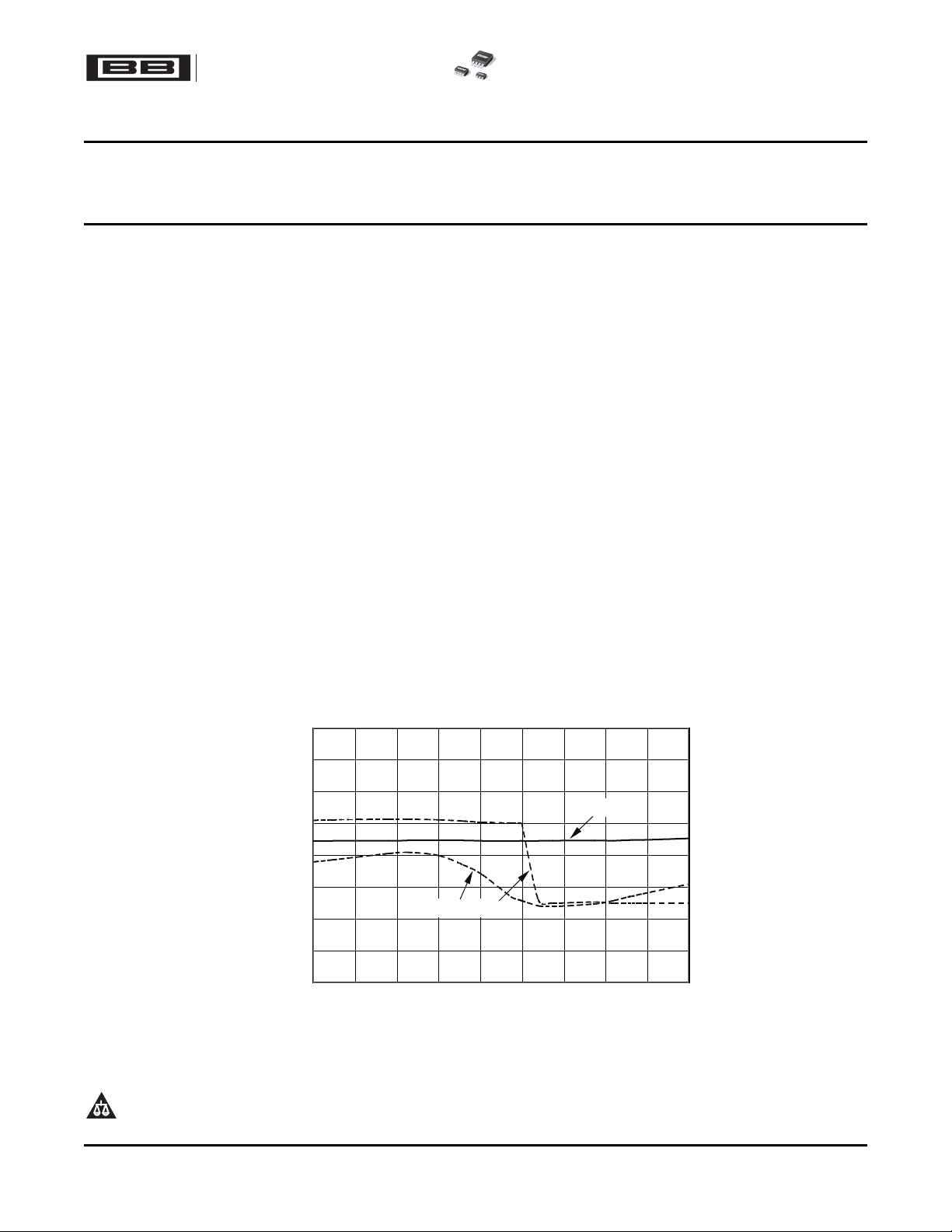
OFFSETVOLTAGE
vsCOMMON-MODEVOLTAGE
(V =1.8V)
S
Common-ModeVoltage(V)
OffsetVoltage( V)
m
0 0.2 0.4 0.6 0.8 1.0 1.2 1.4 1.6 1.8
Competition
OPA369
1.8V, 1 μ A max, Zerø-Crossover
RAIL-TO-RAIL I/O OPERATIONAL AMPLIFIER
1
FEATURES DESCRIPTION
2
• ZERØ-CROSSOVER
• LOW POWER: 1 μ A (max)
• LOW OFFSET VOLTAGE: 750 μ V (max)
• LOW VOLTAGE SUPPLY: +1.8V to +5.5V
• LOW OFFSET DRIFT: 1.75 μ V/ ° C (max)
• microSIZE PACKAGES:
– SC70-5, SOT23-8, MSOP-8
APPLICATIONS
• BATTERY-POWERED INSTRUMENTS
• PORTABLE DEVICES
• MEDICAL INSTRUMENTS
• TEST EQUIPMENT
OPA369
OPA2369
SBOS414A – AUGUST 2007 – REVISED SEPTEMBER 2007
The OPA369 and OPA2369 are new low-power,
low-voltage operational amplifiers from Texas
Instruments designed especially for battery-powered
applications.
The OPAx369 operates on a supply voltage as low as
1.8V and has true rail-to-rail operation that makes it
useful for a wide range of applications. The
zero-crossover feature resolves the problem of input
crossover distortion that becomes very prominent in
low voltage (< 3V), rail-to-rail input applications.
In addition to microsize packages and very low
quiescent current (1 μ A, max) the OPAx369 features
12kHz bandwidth, low offset drift (1.75 μ V/ ° C, max),
and low 0.1Hz to 10Hz noise (3.6 μ V
The OPA369 (single version, available Q4 2007) is
offered in an SC70-5 package. The OPA2369 (dual
version) comes in both MSOP-8 and SOT23-8
packages.
hi laurie
).
PP
1
Please be aware that an important notice concerning availability, standard warranty, and use in critical applications of
Texas Instruments semiconductor products and disclaimers thereto appears at the end of this data sheet.
2 All trademarks are the property of their respective owners.
PRODUCTION DATA information is current as of publication date.
Products conform to specifications per the terms of the Texas
Instruments standard warranty. Production processing does not
necessarily include testing of all parameters.
Copyright © 2007, Texas Instruments Incorporated
Page 2
www.ti.com
1
2
3
5
4
V+
OUT
+IN
V-
-IN
1
2
3
4
8
7
6
5
V+
OutB
-InB
+InB
OutA
-InA
+InA
V-
OPA369
OPA2369
SBOS414A – AUGUST 2007 – REVISED SEPTEMBER 2007
This integrated circuit can be damaged by ESD. Texas Instruments recommends that all integrated circuits be handled with
appropriate precautions. Failure to observe proper handling and installation procedures can cause damage.
ESD damage can range from subtle performance degradation to complete device failure. Precision integrated circuits may be more
susceptible to damage because very small parametric changes could cause the device not to meet its published specifications.
ABSOLUTE MAXIMUM RATINGS
(1)
Over operating free-air temperature range (unless otherwise noted).
VALUE UNIT
Supply Voltage, VS= (V+) – (V – ) +7V V
(2)
Single Input
Terminals
Output Short-Circuit
Operating Temperature, T
Storage Temperature, T
Junction Temperature, T
Voltage
(2)
Current
(3)
A
A
J
Human Body Model (HBM) 4000 V
ESD Ratings Charged Device Model (CDM) 1000 V
Machine Model (MM) 200 V
(1) Stresses above these ratings may cause permanent damage. Exposure to absolute maximum conditions for extended periods may
degrade device reliability. These are stress ratings only, and functional operation of the device at these or any other conditions beyond
those specified is not supported.
(2) Input terminals are diode-clamped to the power-supply rails. Input signals that can swing more than 0.5V beyond the supply rails should
be current limited to 10mA or less.
(3) Short-circuit to VS/2, one amplifier per package.
PACKAGE/ORDERING INFORMATION
PRODUCT PACKAGE-LEAD PACKAGE DESIGNATOR PACKAGE MARKING
OPA369 SC70-5
OPA2369
(1) For the most current package and ordering information see the Package Option Addendum at the end of this document, or see the TI
web site at www.ti.com .
(2) Available Q4, 2007.
(2)
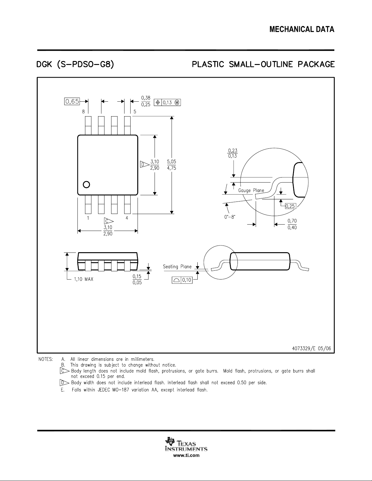
MSOP-8 DGK OCCQ
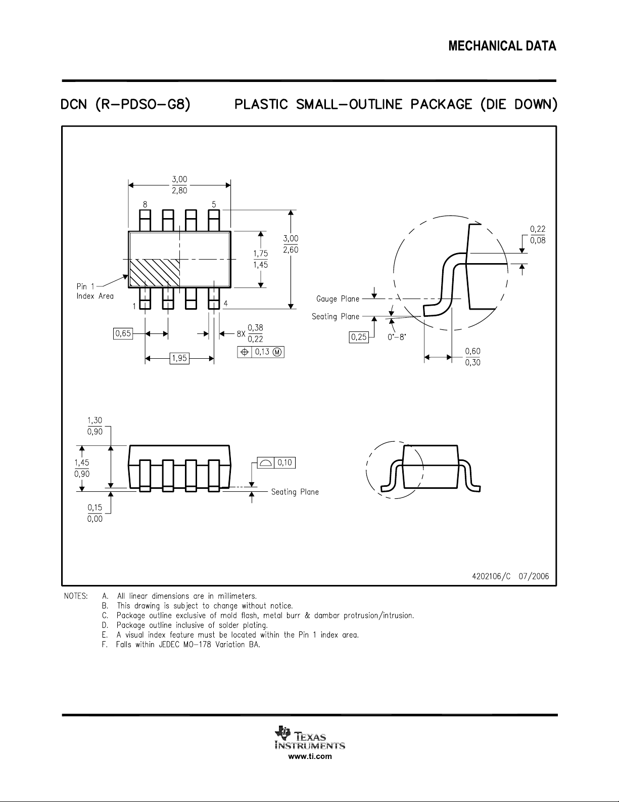
SOT23-8 DCN OCBQ
– 0.5 to (V+) + 0.5 V
± 10 mA
Continuous
– 55 to +125 ° C
– 65 to +150 ° C
+150 ° C
(1)
DCK CJS
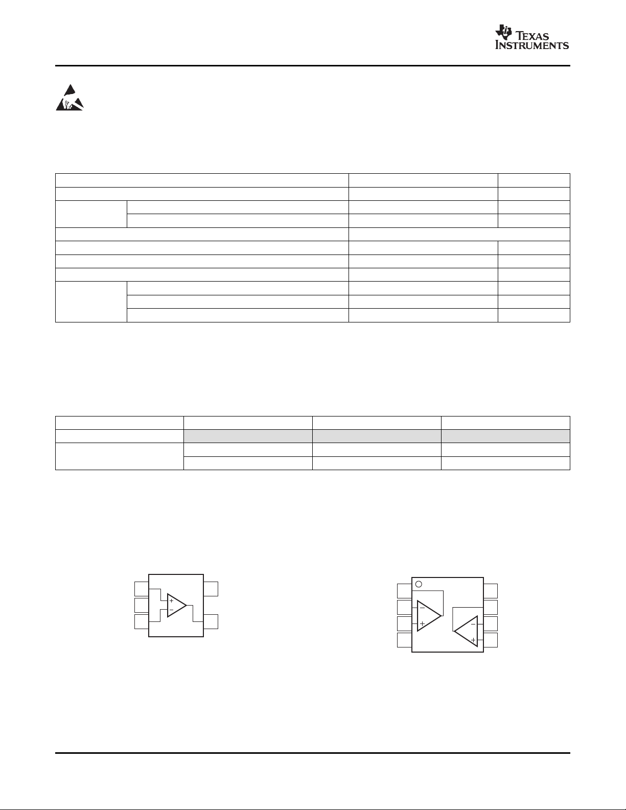
PIN CONFIGURATIONS
OPA369
(TOP VIEW)
(1) Available Q4, 2007.
2 Submit Documentation Feedback Copyright © 2007, Texas Instruments Incorporated
(1)
SC70-5
OPA2369
MSOP-8, SOT23-8
(TOP VIEW)
Product Folder Link(s): OPA369 OPA2369
Page 3

www.ti.com
OPA369
OPA2369
SBOS414A – AUGUST 2007 – REVISED SEPTEMBER 2007
ELECTRICAL CHARACTERISTICS: V
= +1.8V to +5.5V
S
BOLDFACE limits apply over the specified temperature range, TA= – 40 ° C to +85 ° C.
At TA= +25 ° C, RL= 100k Ω connected to VS/2, unless otherwise noted.
(1)
OPA369
PARAMETER CONDITIONS MIN TYP MAX UNIT
OFFSET VOLTAGE
Input Offset Voltage V
OS
over Temperature 1 mV
Drift dV
/dT 0.4 1.75 μ V/ ° C
OS
vs Power Supply PSRR VS= 1.8V to 5.5V 5 20 μ V/V
Channel Separation dc 0.1 μ V/V
f = 1kHz 120 dB
INPUT VOLTAGE RANGE
Common-Mode Voltage Range V
CM
(V – ) (V+) V
Common-Mode Rejection Ratio CMRR (V – ) ≤ VCM≤ (V+) 100 114 dB
over Temperature (V – ) ≤ VCM≤ (V+) 90 dB
INPUT BIAS CURRENT
Input Bias Current I
Input Offset Current I
B
OS
INPUT IMPEDANCE
Differential
Common-Mode
NOISE
Input Voltage Noise f = 0.1Hz to 10Hz 3.6 μ V
Input Voltage Noise Density f = 100Hz 160 nV/ √ Hz
f = 1kHz 120 nV/ √ Hz
Current Noise Density f = 1kHz 1 fA/ √ Hz
OPEN-LOOP GAIN
Open-Loop Voltage Gain A
Over Temperature 100mV ≤ VO≤ (V+) – 100mV, RL=
Over Temperature 500mV ≤ VO≤ (V+) – 500mV, RL=
100mV ≤ VO≤ (V+) – 100mV, RL=
OL
100k Ω
100k Ω
500mV ≤ VO≤ (V+) – 500mV, RL=
114 134 dB
100 dB
10k Ω
10k Ω
114 134 dB
90 d B
OUTPUT
Voltage Output Swing from Rail RL= 100k Ω 10 mV
RL= 10k Ω 25 mV
Short-Circuit Current I
Capacitive Load Drive C
SC
LOAD
See Typical Characteristics pF
FREQUENCY RESPONSE
Gain-Bandwidth Product GBW 12 kHz
Slew Rate SR G = +1 0.005 V/ μ s
Overload Recovery Time VIN× Gain > V
S
POWER SUPPLY
Specified Voltage V
Quiescent Current
(per channel amplifier)
S
I
Q
I
= 0A 0.7 1 μ A
OUT
1.8 5.5 V
Over Temperature 1.25 μ A
(1) OPA369 specifications are preview. Available Q4, 2007.
, OPA2369
250 750 μ V
10 50 pA
10 50 pA
13
10
|| 3
13
10
|| 6
10 mA
250 μ s
Ω || pF
Ω || pF
PP
Copyright © 2007, Texas Instruments Incorporated Submit Documentation Feedback 3
Product Folder Link(s): OPA369 OPA2369
Page 4

www.ti.com
OPA369
OPA2369
SBOS414A – AUGUST 2007 – REVISED SEPTEMBER 2007
ELECTRICAL CHARACTERISTICS: V
= +1.8V to +5.5V (continued)
S
BOLDFACE limits apply over the specified temperature range, TA= – 40 ° C to +85 ° C.
At TA= +25 ° C, RL= 100k Ω connected to VS/2, unless otherwise noted.
(1)
OPA369
PARAMETER CONDITIONS MIN TYP MAX UNIT
TEMPERATURE RANGE
Specified Range T
Operating Range T
Thermal Resistance θ
SC70 250 ° C/W
SOT23 223 ° C/W
MSOP 252 ° C/W
JA
A
A
– 40 +85 ° C
– 55 +125 ° C
, OPA2369
4 Submit Documentation Feedback Copyright © 2007, Texas Instruments Incorporated
Product Folder Link(s): OPA369 OPA2369
Page 5
www.ti.com
Population
OffsetVoltage( V)m
-750
-
675
-600
-525
-450
-
375
-300
-225
-
150
-75
0
75
150
225
300
375
450
525
600
675
750
-1.2
Population
OffsetVoltageDrift( V/ C)m °
-1.1
-1.0
-0.9
-0.8
-0.7
-0.6
-0.5
-0.4
-0.3
-0.2
-0.1
0
0.1
0.2
0.3
0.4
0.5
0.6
0.7
0.8
0.9
1.0
1.1
1.2
1000
800
600
400
200
0
-200
-400
-600
-800
-1000
Temperature( C)°
OffsetVoltage( V)m
-75 100 125-50 -25 0 25 50 75
Normalized OffsetVoltage m( V)
100
80
60
40
20
0
-20
-40
-60
-80
-100
Common-ModeVoltage (V)
-0.2
0
0.2
0.4
0.6
0.8
1.0
1.2
1.4
1.6
1.8
2.0
2.2
2.4
2.6
2.8
3.0
3.2
3.4
3.6
3.8
4.0
4.2
4.4
4.6
4.8
5.0
5.2
V =5V
S
10TypicalUnitsShown
1m
V/div
Time(500ms/div)
10000
1000
100
10
Frequency(Hz)
V
oltageNoise,RTI(nV/ )
ÖHz
0.1 100101 1k
SBOS414A – AUGUST 2007 – REVISED SEPTEMBER 2007
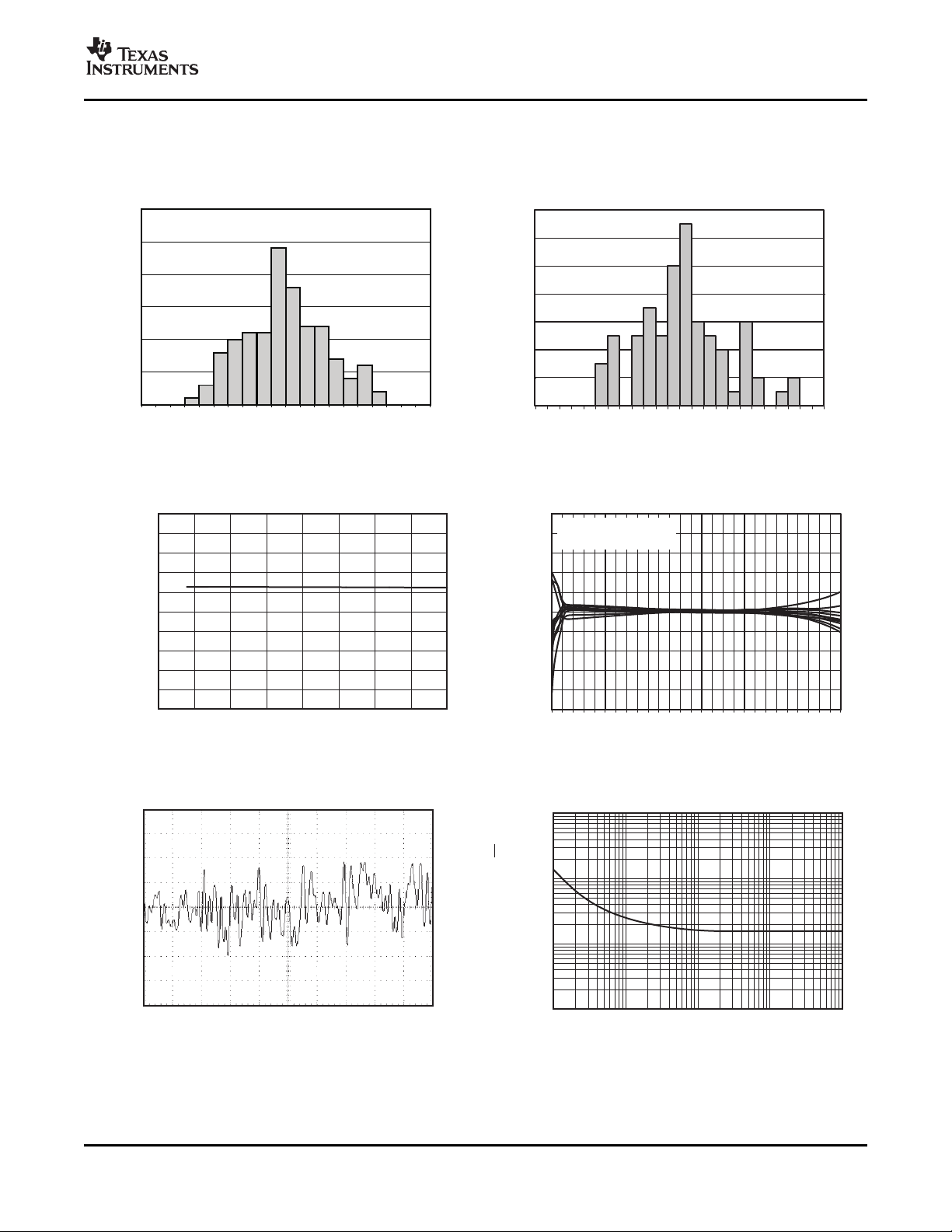
TYPICAL CHARACTERISTICS
At TA= +25 ° C, VS= 5V, RL= 100k Ω connected to VS/2, unless otherwise noted.
OFFSET VOLTAGE OFFSET VOLTAGE DRIFT
PRODUCTION DISTRIBUTION PRODUCTION DISTRIBUTION
Figure 1. Figure 2.
OPA369
OPA2369
OFFSET VOLTAGE vs TEMPERATURE vs COMMON-MODE VOLTAGE
NORMALIZED OFFSET VOLTAGE
Figure 3. Figure 4.
INPUT-REFERRED VOLTAGE NOISE
0.1Hz to 10Hz NOISE vs FREQUENCY
Copyright © 2007, Texas Instruments Incorporated Submit Documentation Feedback 5
Figure 5. Figure 6.
Product Folder Link(s): OPA369 OPA2369
Page 6
www.ti.com
140
120
100
80
60
40
20
0
-20
Frequency(Hz)
Gain(dB)
0.001 100 1k100.1 10.01 20k10k
PHASE
GAIN
180
135
90
45
0
Phase( )
°
110
100
90
80
70
60
50
40
30
20
10
0
Frequency(Hz)
PSRR(dB)
1 1k 10k10010 20k
+PSRR
-PSRR
120
100
80
60
40
20
0
Frequency(Hz)
CMRR(dB)
10 10k1k100 20k
160
140
120
100
80
60
40
20
0
Frequency(Hz)
ChannelSeparation(dB)
100 10k1k 100k
20
15
10
5
0
-5
-10
-15
-20
Temperature( C)°
PSRR( V/V)m
-75 -50 -25 0 25 50 75 100 125
10TypicalUnitsShown
10
8
6
4
2
0
Temperature( C)°
CMRR( V/V)m
-75 100 125-50 -25 0 25 50 75
OPA369
OPA2369
SBOS414A – AUGUST 2007 – REVISED SEPTEMBER 2007
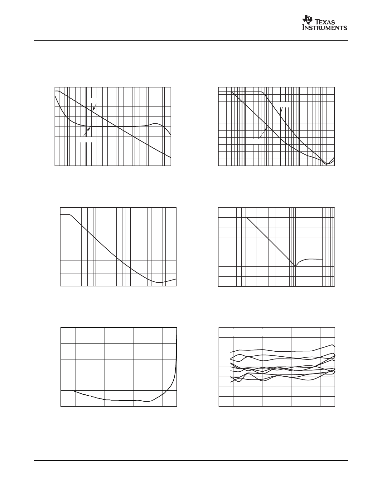
TYPICAL CHARACTERISTICS (continued)
At TA= +25 ° C, VS= 5V, RL= 100k Ω connected to VS/2, unless otherwise noted.
OPEN-LOOP GAIN AND PHASE POWER-SUPPLY REJECTION RATIO
vs FREQUENCY vs FREQUENCY
Figure 7. Figure 8.
COMMON-MODE REJECTION RATIO
vs FREQUENCY CHANNEL SEPARATION vs FREQUENCY
Figure 9. Figure 10.
COMMON-MODE REJECTION RATIO POWER-SUPPLY REJECTION RATIO
vs TEMPERATURE vs TEMPERATURE
6 Submit Documentation Feedback Copyright © 2007, Texas Instruments Incorporated
Figure 11. Figure 12.
Product Folder Link(s): OPA369 OPA2369
Page 7
www.ti.com
3.0
2.5
2.0
1.5
1.0
0.5
0
Temperature( C)°
A ( V/V)m
OL
-75 -50 -25 0 25 50 75 100 125
R =10kW
L
R =100kW
L
25
20
15
10
5
0
-5
-10
-15
-20
-25
Temperature( C)°
OutputVoltageSwing-from-Rail(mV)
-75 100 125-50 -25 0 25 50 75
R =10kW
L
R =100kW
L
InputBiasCurrent(pA)
-50
10k
1k
100
10
1
0.1
0.01
Temperature( C)°
125-25 0 25 50 75 100
OutputVoltage(V)
0
2.75
2.25
1.75
1.25
0.75
0.25
-0.25
-0.75
-1.25
-1.75
-2.25
-2.75
OutputCurrent(mA)
455 3010 15 20 25 35 40
+115 C°
+85 C°
+25 C°
-40°C
V = 2.75V
S
±
2.0
1.5
1.0
0.5
0
Temperature( C)°
QuiescentCurrent(
A)m
-75 100-50 -25 0 25 50 75 125
3.0
2.5
2.0
1.5
1.0
0.5
0
Frequency(Hz)
MaximumV (V)
OUT
100 1k 2k
TYPICAL CHARACTERISTICS (continued)
At TA= +25 ° C, VS= 5V, RL= 100k Ω connected to VS/2, unless otherwise noted.
OPA369
OPA2369
SBOS414A – AUGUST 2007 – REVISED SEPTEMBER 2007
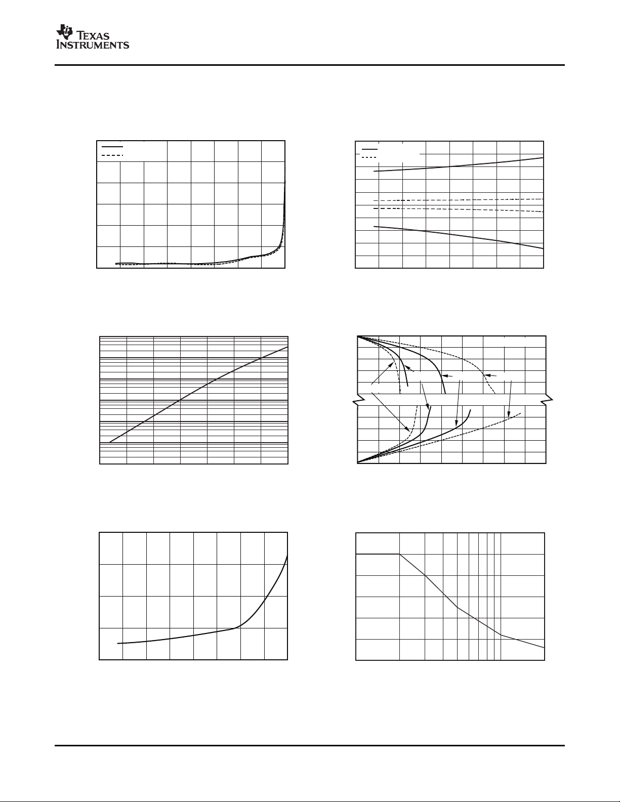
OPEN-LOOP GAIN vs TEMPERATURE vs TEMPERATURE
Figure 13. Figure 14.
INPUT BIAS CURRENT OUTPUT VOLTAGE
vs TEMPERATURE vs OUTPUT CURRENT
OUTPUT VOLTAGE SWING-FROM-RAIL
Figure 15. Figure 16.
QUIESCENT CURRENT vs TEMPERATURE vs FREQUENCY
Copyright © 2007, Texas Instruments Incorporated Submit Documentation Feedback 7
Figure 17. Figure 18.
MAXIMUM OUTPUT VOLTAGE
Product Folder Link(s): OPA369 OPA2369
Page 8
www.ti.com
20mV/div
Time(100 s/div)m
C =20pF
L
50
40
30
20
10
0
CapacitiveLoad(pF)
Overshoot(%)
10 100 200
G=+1
500mV/div
Time(250 s/div)m
1V/div
Time(500 s/div)m
C =200pF
L
OPA369
OPA2369
SBOS414A – AUGUST 2007 – REVISED SEPTEMBER 2007
TYPICAL CHARACTERISTICS (continued)
At TA= +25 ° C, VS= 5V, RL= 100k Ω connected to VS/2, unless otherwise noted.
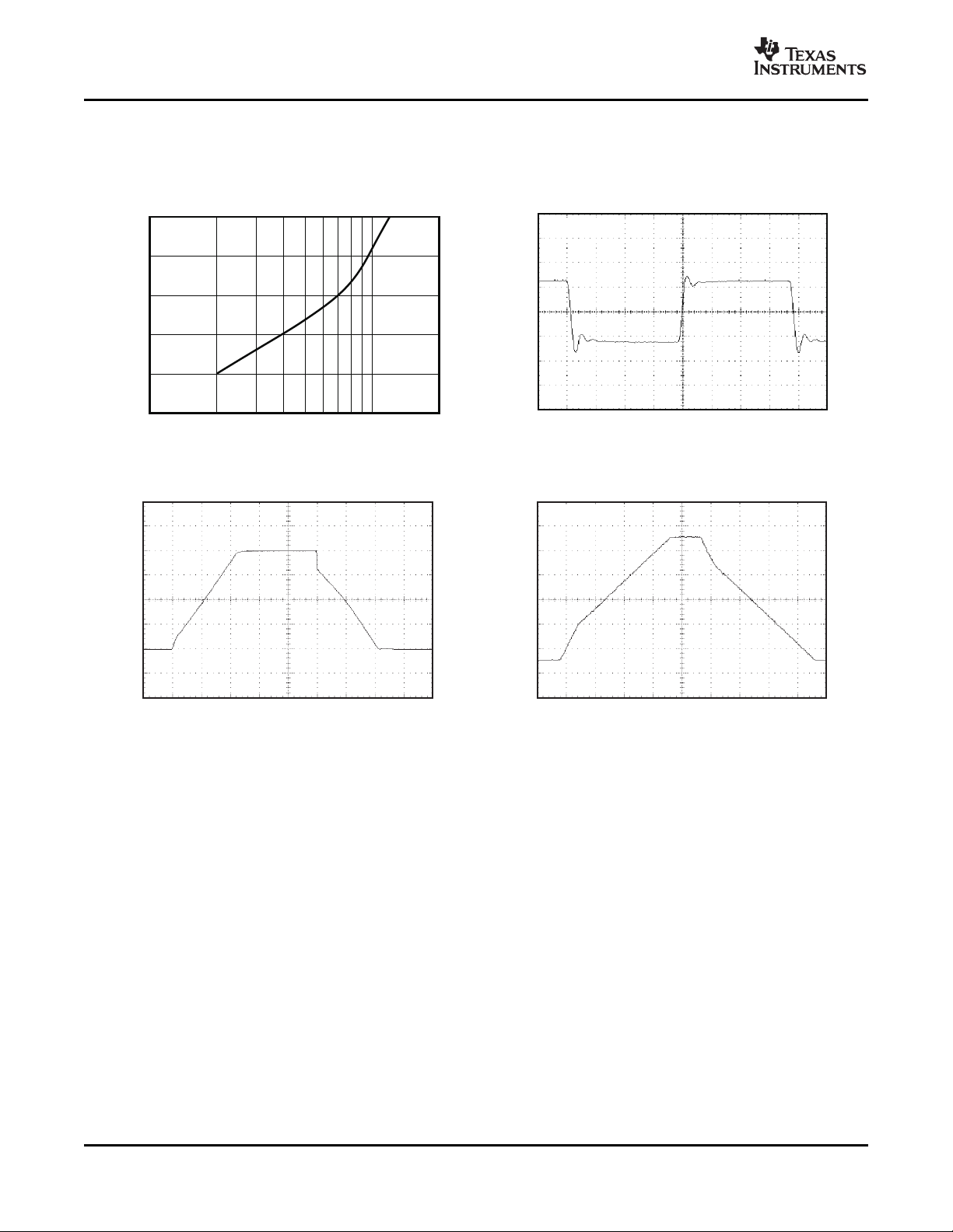
SMALL-SIGNAL OVERSHOOT
vs CAPACITIVE LOAD SMALL-SIGNAL STEP RESPONSE
Figure 19. Figure 20.
LARGE-SIGNAL STEP RESPONSE OVERLOAD RECOVERY
Figure 21. Figure 22.
8 Submit Documentation Feedback Copyright © 2007, Texas Instruments Incorporated
Product Folder Link(s): OPA369 OPA2369
Page 9
www.ti.com
5kW
OPA369
10mAmax
+5V
V
IN
V
OUT
I
OVERLOAD
Current-limitingresistor
requiredifinputvoltage
exceedssupplyrailsby
³ 0.5V.
10 toW
20W
OPA369
V+
V
IN
V
OUT
R
S
R
L
C
L
The OPA369 family of operational amplifiers
minimizes power consumption and operates on
supply voltages as low as 1.8V. Power-supply
rejection ratio (PSRR), common-mode rejection ratio
(CMRR), and open-loop gain (A
in the range of 100dB or better.
When designing for ultralow power, choose system
components carefully. To minimize current
consumption, select large-value resistors. However,
note that large resistors will react with stray
capacitance in the circuit and the input capacitance of
the operational amplifier. These parasitic RC
combinations can affect the stability of the overall
system. A feedback capacitor may be required to
assure stability and limit overshoot or gain peaking.
Good layout practice and use of a 0.1 μ F bypass
capacitor placed closely across the supply pins are
mandatory.
OPERATING VOLTAGE
OPA369 series op amps are fully specified and tested
from +1.8V to +5.5V. Parameters that vary
significantly with supply voltage are shown in the
Typical Characteristic curves.
INPUT COMMON-MODE VOLTAGE RANGE
The OPA369 family is designed to eliminate the input
offset transition region typically present in most
rail-to-rail complementary stage operational
amplifiers, which allows the OPA369 family of
amplifiers to provide superior common-mode
performance over the entire input range.
The input common-mode voltage range of the
OPA369 family typically extends to each supply rail.
CMRR is specified from the negative rail to the
positive rail. See Figure 4 the Normalized Offset
Voltage vs Common-Mode Voltage.
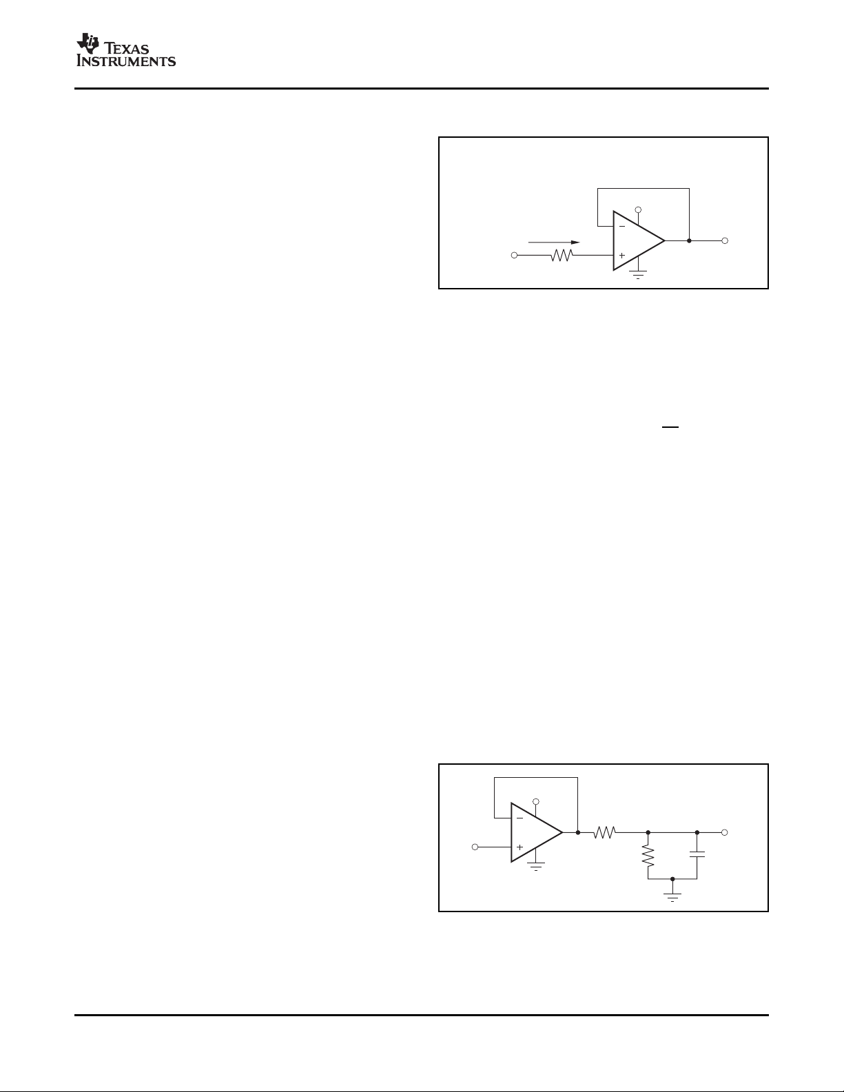
PROTECTING INPUTS FROM OVER-VOLTAGE
Input currents are typically 10pA. However, large
inputs (greater than 500mV beyond the supply rails)
can cause excessive current to flow in or out of the
input pins. Therefore, in addition to keeping the input
voltage between the supply rails, it is also important
to limit the input current to less than 10mA. This
limiting is easily accomplished with an input resistor,
as shown in Figure 23 .
Copyright © 2007, Texas Instruments Incorporated Submit Documentation Feedback 9
OPA369
OPA2369
SBOS414A – AUGUST 2007 – REVISED SEPTEMBER 2007
APPLICATION INFORMATION
) typical values are
OL
Figure 23. Input Current Protection for Voltages
Exceeding the Supply Voltage
NOISE
Although micropower amplifiers frequently have high
wideband noise, the OPA369 series offers excellent
noise performance. The OPA369 has only 2.8 μ V
0.1Hz to 10Hz noise, and 80nV/ Hz of wideband
noise. Resistors should be chosen carefully, because
they can become the dominant source of noise.
CAPACITIVE LOAD AND STABILITY
Follower configurations with load capacitance in
excess of approximately 50pF can produce extra
overshoot and ringing in the output signal (see
Figure 19 ). Increasing the gain enhances the ability of
the amplifier to drive greater capacitive loads. In
unity-gain configurations, capacitive load drive can be
improved by inserting a small (10 Ω to 20 Ω ) resistor,
RS, in series with the output, as shown in Figure 24 .
This resistor significantly reduces ringing while
maintaining dc performance for purely capacitive
loads. However, if there is a resistive load in parallel
with the capacitive load, a voltage divider is created,
introducing a dc error at the output and slightly
reducing the output swing. The error introduced is
proportional to the ratio RS/R
negligible.
Figure 24. Series Resistor in Unity-Gain Buffer
Configuration Improves Capacitive Load Drive
Product Folder Link(s): OPA369 OPA2369
, and is generally
L
of
PP
Page 10
www.ti.com
R =
F
V
REF
1000(I
BMAX
)
=
1.2V
1000(50pA)
= 24M 20MW W»
R =R
1
F
=20MW
V
HYST
V
BATT
=420kW
50mV
2.4V
R
I
OPA369
V
IN
V
OUT
RF
C
FB
C
IN
R =
2
-
V
THRS
V
BATT
1
R
1
1
( )
-
1
R
1
=
-
2V
1.2V 420kW´
1
420kW
1
( )
-
1
20MW
= 650kW
R =
BIAS
=0.9MW
V
BATTMIN
I
BIAS
=
1.8V
2 Am
REF1112
OPA369
+IN
OUT
-IN
V
STATUS
V
BATT
V
REF
R
1
R
2
R
BIAS
I
BIAS
R
F
+
OPA369
OPA2369
SBOS414A – AUGUST 2007 – REVISED SEPTEMBER 2007
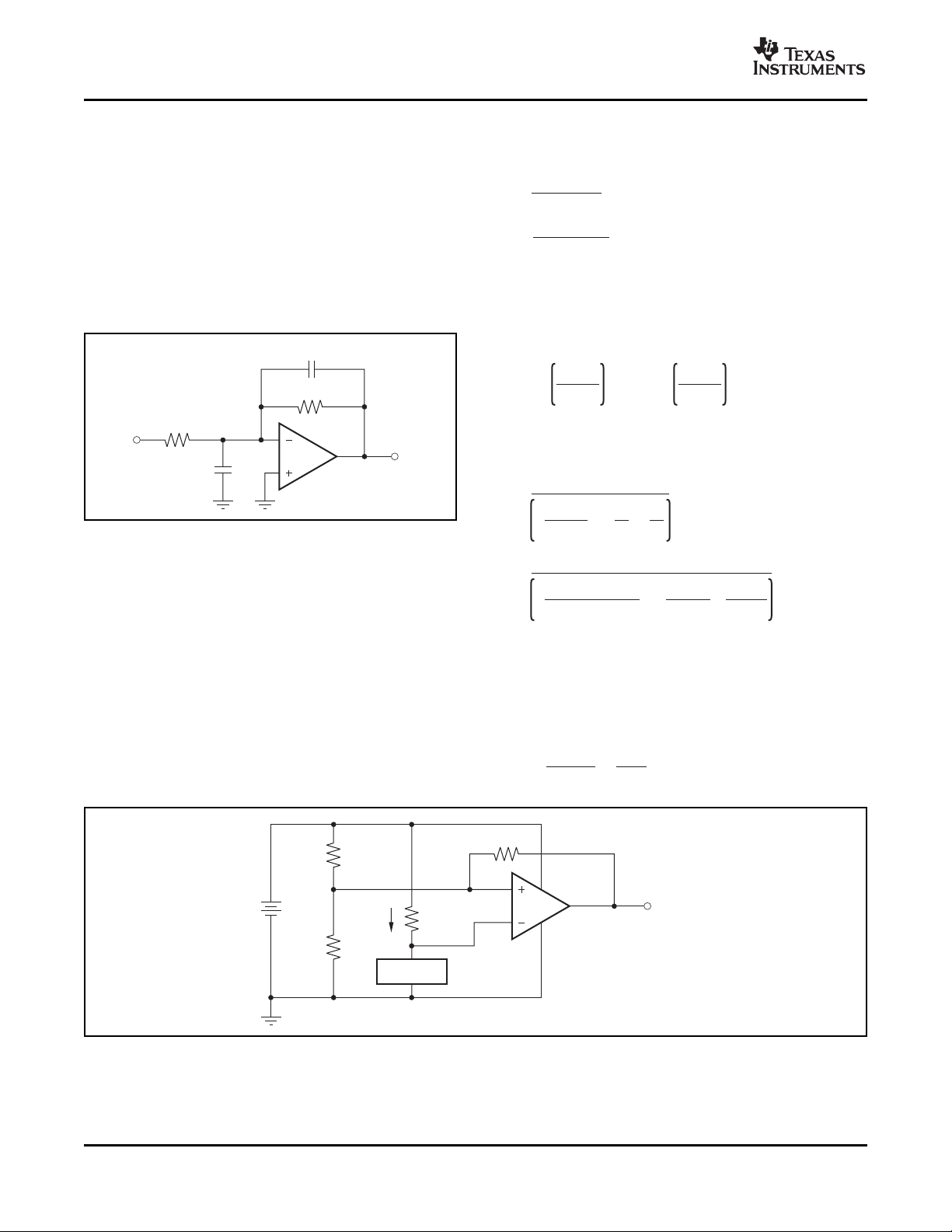
In unity-gain inverter configuration, phase margin can 1. Selecting RF: Select R
be reduced by the reaction between the capacitance through R
is approximately 1000x larger than
F
at the op amp input and the gain setting resistors. the maximum bias current over temperature:
Best performance is achieved by using smaller
valued resistors. However, when larger valued
resistors cannot be avoided, a small (4pF to 6pF)
capacitor, C
, can be inserted in the feedback, as
FB
shown in Figure 25 . This configuration significantly
reduces overshoot by compensating the effect of
capacitance, C
capacitance and printed circuit board (PCB) parasitic
capacitance.
, which includes the amplifier input
IN
2. Choose the hysteresis voltage, V
battery-monitoring applications, 50mV is
adequate.
3. Calculate R
as follows:
1
4. Select a threshold voltage for V
2.0V
Figure 25. Improving Stability for Large R
5. Calculate R
and R
F
IN
as follows:
2
such that the current
F
(1)
. For
HYST
(2)
rising (V
IN
) =
THRS
BATTERY MONITORING
The low operating voltage and quiescent current of
the OPA369 series make it an excellent choice for
battery monitoring applications, as shown in
Figure 26 . In this circuit, V
STATUS
is high as long as
the battery voltage remains above 2V. A low-power
reference is used to set the trip point. Resistor values
are selected as follows:
10 Submit Documentation Feedback Copyright © 2007, Texas Instruments Incorporated
Figure 26. Battery Monitor
Product Folder Link(s): OPA369 OPA2369
6. Calculate R
: The minimum supply voltage for
BIAS
this circuit is 1.8V. The REF1112 has a current
requirement of 1.2 μ A (max). Providing the
REF1112 with 2 μ A of supply current assures
proper operation. Therefore:
(3)
(4)
Page 11
www.ti.com
V =
H
R
2
R + R
1 2
V =
L
R
4
R + R
3 4
3V
A1
A2
D1
(2)
D2
(2)
R
5
10kW
R
6
5.1kW
R
7
5.1kW
R
IN
2kW
(1)
3V
3V
Q1
(3)
R
1
V
H
V
L
R
2
1/2
OPA2369
1/2
OPA2369
3V
V
OUT
V
IN
3V
R
3
R
4
NOTES: (1)R protectsA1andA2frompossibleexcesscurrentflow.
IN
(2)IN4446orequivalentdiodes.
(3)2N2222orequivalentNPNtransistor.
R
1
V
EX
V
OUT
V
REF
R
1
OPA369
R
R
R R
+5V
OPA369
OPA2369
SBOS414A – AUGUST 2007 – REVISED SEPTEMBER 2007
WINDOW COMPARATOR
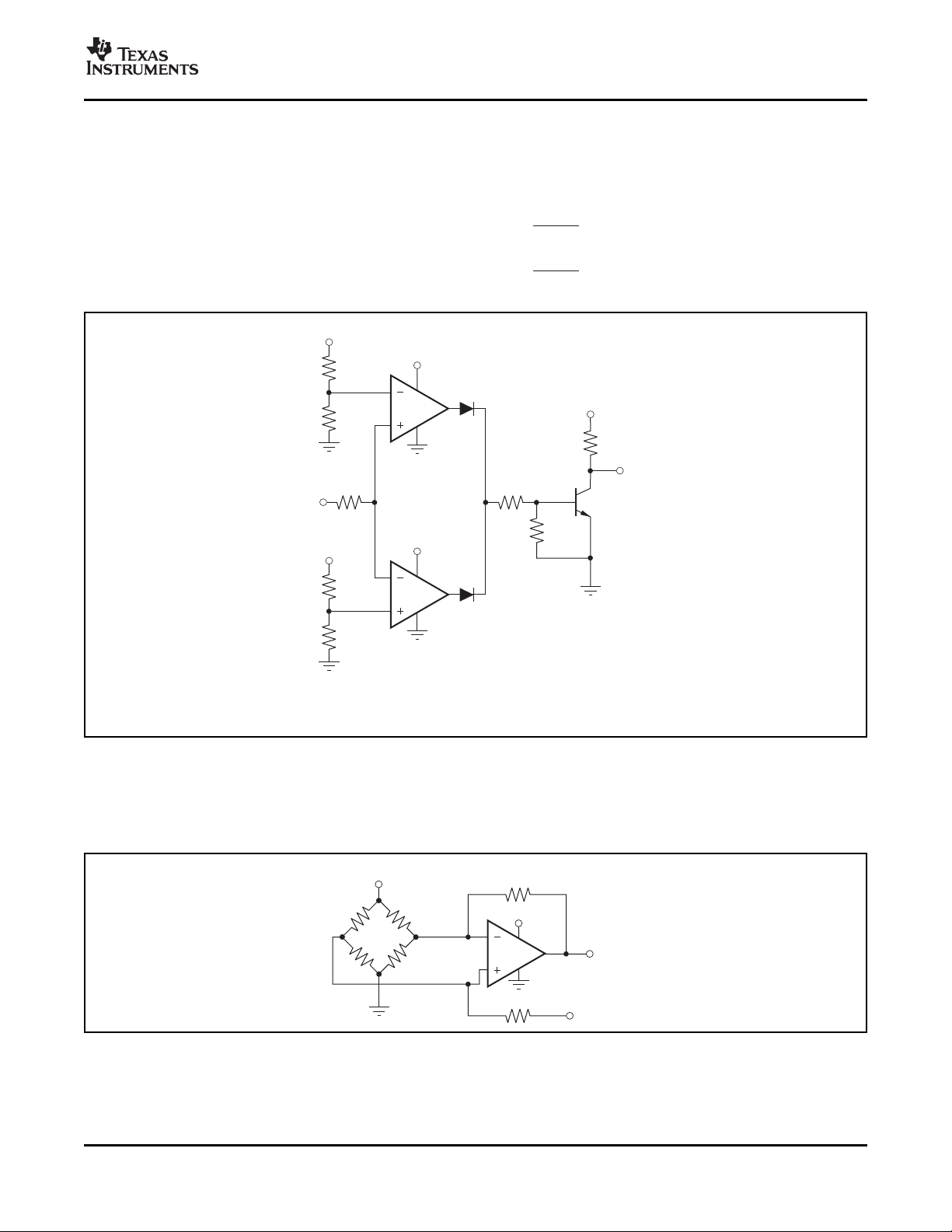
Figure 27 shows the OPA2369 used as a window
comparator. The threshold limits are set by V
VL, with V
low. When V
> VL. When V
H
IN
<
, the output of A1 is
IN
>V
, the output of A2 is low.
L
VH
Therefore, both op amp outputs are at 0V as long as
V
is between V
IN
and VL. This configuration results
H
in no current flowing through either diode, Q1 in
cutoff, with the base voltage at 0V, and V
high.
H
forced
OUT
If V
falls below VL, the output of A2 is high, current
IN
flows through D2, and V
and
rises above VH, the output of A1 is high, current flows
through D1, and V
OUT
is low. The window comparator
is low. Likewise, if V
OUT
IN
threshold voltages are set as follows:
(5)
(6)
Figure 27. OPA2369 as a Window Comparator
ADDITIONAL APPLICATION EXAMPLES
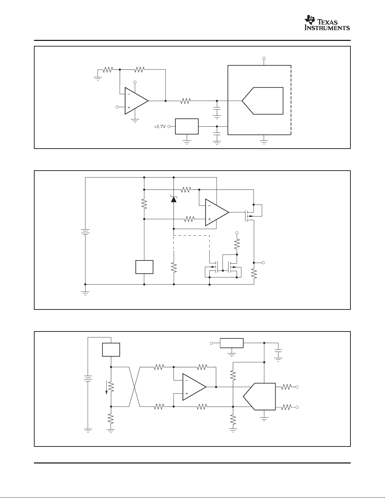
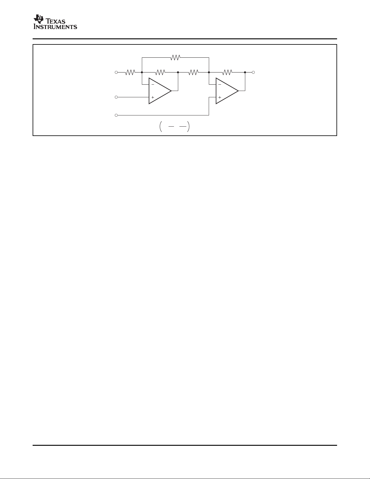
Figure 28 through Figure 32 illustrate additional application examples.
Copyright © 2007, Texas Instruments Incorporated Submit Documentation Feedback 11
Figure 28. Single Op Amp Bridge Amplifier
Product Folder Link(s): OPA369 OPA2369
Page 12
www.ti.com
R
3
R
2
V
IN
+2.7V
R
66.51W
C
1.5nF
1
C
1 F2m
VREF
A0+
REF3312
+2.7V
V
CC
V
SS
16-Bit
ADC
MSP430x20x3PW
OPA369
OPA369
Output
R
SHUNT
Load
V+
V+
R
G
R
L
R
(2)
1
10kW
R
BIAS
+5V
zener
(1)
Twozener
biasingmethods
areshown.
(3)
MOSFETratedto
stand-offsupplyvoltage
suchasBSS84for
upto50V.
(1)Zenerratedforopampsupplycapability(thatis,5.1VforOPA369).
(2)Current-limitingresistor.
(3)ChoosezenerbiasingresistorordualNMOSFETs(FDG6301N,NTJD4001N,orSi1034)
NOTES:
NOTE:1%resistorsprovideadequatecommon-moderejectionatsmallground-looperrors.
OPA369
ADS1100
Load
V
I C
2
R
1
4.99kW
R
3
4.99kW
R
4
48.7kW
R
2
49.9kW
+5V
3V
REF3130
R
7
1.18kW
R
SHUNT
1W
R
6
71.5kW
R
N
56W
R
N
56W
(PGAGain=4)
FS=3.0V
StrayGround-LoopResistance
I
LOAD
OPA369
OPA2369
SBOS414A – AUGUST 2007 – REVISED SEPTEMBER 2007
Figure 29. Unipolar Signal Chain Configuration
Figure 30. High-Side Current Monitor
12 Submit Documentation Feedback Copyright © 2007, Texas Instruments Incorporated
Figure 31. Low-Side Current Monitor
Product Folder Link(s): OPA369 OPA2369
Page 13
www.ti.com
R
2
V = (V - V )1+++V
OUT 1 2 REF
R
1
R
2
R
G
R
2
R
1
V
REF
V
OUT
V
2
V
1
R
1
1/2
OPA2369
1/2
OPA2369
2R
1
R
G
Figure 32. Two Op Amp Instrumentation Amplifier
OPA369
OPA2369
SBOS414A – AUGUST 2007 – REVISED SEPTEMBER 2007
Copyright © 2007, Texas Instruments Incorporated Submit Documentation Feedback 13
Product Folder Link(s): OPA369 OPA2369
Page 14

PACKAGE OPTION ADDENDUM
www.ti.com
27-Aug-2007
PACKAGING INFORMATION
Orderable Device Status
(1)
Package
Type
Package
Drawing
Pins Package
Qty
Eco Plan
OPA2369AIDCNR PREVIEW SOT-23 DCN 8 3000 TBD Call TI Call TI
OPA2369AIDCNT PREVIEW SOT-23 DCN 8 250 TBD Call TI Call TI
OPA2369AIDGKR PREVIEW MSOP DGK 8 2500 TBD Call TI Call TI
OPA2369AIDGKT PREVIEW MSOP DGK 8 250 TBD Call TI Call TI
OPA369AIDCKR PREVIEW SC70 DCK 5 3000 TBD Call TI Call TI
OPA369AIDCKT PREVIEW SC70 DCK 5 250 TBD Call TI Call TI
(1)
The marketing status values are defined as follows:
ACTIVE: Product device recommended for new designs.
LIFEBUY: TI has announced that the device will be discontinued, and a lifetime-buy period is in effect.
NRND: Not recommended for new designs. Device is in production to support existing customers, but TI does not recommend using this part in
a new design.
PREVIEW: Device has been announced but is not in production. Samples may or may not be available.
OBSOLETE: TI has discontinued the production of the device.
(2)
Eco Plan - The planned eco-friendly classification: Pb-Free (RoHS), Pb-Free (RoHS Exempt), or Green (RoHS & no Sb/Br) - please check
http://www.ti.com/productcontent for the latest availability information and additional product content details.
TBD: The Pb-Free/Green conversion plan has not been defined.
Pb-Free (RoHS): TI's terms "Lead-Free" or "Pb-Free" mean semiconductor products that are compatible with the current RoHS requirements
for all 6 substances, including the requirement that lead not exceed 0.1% by weight in homogeneous materials. Where designed to be soldered
at high temperatures, TI Pb-Free products are suitable for use in specified lead-free processes.
Pb-Free (RoHS Exempt): This component has a RoHS exemption for either 1) lead-based flip-chip solder bumps used between the die and
package, or 2) lead-based die adhesive used between the die and leadframe. The component is otherwise considered Pb-Free (RoHS
compatible) as defined above.
Green (RoHS & no Sb/Br): TI defines "Green" to mean Pb-Free (RoHS compatible), and free of Bromine (Br) and Antimony (Sb) based flame
retardants (Br or Sb do not exceed 0.1% by weight in homogeneous material)
(2)
Lead/Ball Finish MSL Peak Temp
(3)
(3)
MSL, Peak Temp. -- The Moisture Sensitivity Level rating according to the JEDEC industry standard classifications, and peak solder
temperature.
Important Information and Disclaimer:The information provided on this page represents TI's knowledge and belief as of the date that it is
provided. TI bases its knowledge and belief on information provided by third parties, and makes no representation or warranty as to the
accuracy of such information. Efforts are underway to better integrate information from third parties. TI has taken and continues to take
reasonable steps to provide representative and accurate information but may not have conducted destructive testing or chemical analysis on
incoming materials and chemicals. TI and TI suppliers consider certain information to be proprietary, and thus CAS numbers and other limited
information may not be available for release.
In no event shall TI's liability arising out of such information exceed the total purchase price of the TI part(s) at issue in this document sold by TI
to Customer on an annual basis.
Addendum-Page 1
Page 15
Page 16
Page 17
Page 18

IMPORTANT NOTICE
Texas Instruments Incorporated and its subsidiaries (TI) reserve the right to make corrections, modifications, enhancements,
improvements, and other changes to its products and services at any time and to discontinue any product or service without notice.
Customers should obtain the latest relevant information before placing orders and should verify that such information is current and
complete. All products are sold subject to TI’s terms and conditions of sale supplied at the time of order acknowledgment.
TI warrants performance of its hardware products to the specifications applicable at the time of sale in accordance with TI’s
standard warranty. Testing and other quality control techniques are used to the extent TI deems necessary to support this
warranty. Except where mandated by government requirements, testing of all parameters of each product is not necessarily
performed.
TI assumes no liability for applications assistance or customer product design. Customers are responsible for their products and
applications using TI components. To minimize the risks associated with customer products and applications, customers should
provide adequate design and operating safeguards.
TI does not warrant or represent that any license, either express or implied, is granted under any TI patent right, copyright, mask
work right, or other TI intellectual property right relating to any combination, machine, or process in which TI products or services
are used. Information published by TI regarding third-party products or services does not constitute a license from TI to use such
products or services or a warranty or endorsement thereof. Use of such information may require a license from a third party under
the patents or other intellectual property of the third party, or a license from TI under the patents or other intellectual property of TI.
Reproduction of TI information in TI data books or data sheets is permissible only if reproduction is without alteration and is
accompanied by all associated warranties, conditions, limitations, and notices. Reproduction of this information with alteration is an
unfair and deceptive business practice. TI is not responsible or liable for such altered documentation. Information of third parties
may be subject to additional restrictions.
Resale of TI products or services with statements different from or beyond the parameters stated by TI for that product or service
voids all express and any implied warranties for the associated TI product or service and is an unfair and deceptive business
practice. TI is not responsible or liable for any such statements.
TI products are not authorized for use in safety-critical applications (such as life support) where a failure of the TI product would
reasonably be expected to cause severe personal injury or death, unless officers of the parties have executed an agreement
specifically governing such use. Buyers represent that they have all necessary expertise in the safety and regulatory ramifications
of their applications, and acknowledge and agree that they are solely responsible for all legal, regulatory and safety-related
requirements concerning their products and any use of TI products in such safety-critical applications, notwithstanding any
applications-related information or support that may be provided by TI. Further, Buyers must fully indemnify TI and its
representatives against any damages arising out of the use of TI products in such safety-critical applications.
TI products are neither designed nor intended for use in military/aerospace applications or environments unless the TI products are
specifically designated by TI as military-grade or "enhanced plastic." Only products designated by TI as military-grade meet military
specifications. Buyers acknowledge and agree that any such use of TI products which TI has not designated as military-grade is
solely at the Buyer's risk, and that they are solely responsible for compliance with all legal and regulatory requirements in
connection with such use.
TI products are neither designed nor intended for use in automotive applications or environments unless the specific TI products
are designated by TI as compliant with ISO/TS 16949 requirements. Buyers acknowledge and agree that, if they use any
non-designated products in automotive applications, TI will not be responsible for any failure to meet such requirements.
Following are URLs where you can obtain information on other Texas Instruments products and application solutions:
Products Applications
Amplifiers amplifier.ti.com Audio www.ti.com/audio
Data Converters dataconverter.ti.com Automotive www.ti.com/automotive
DSP dsp.ti.com Broadband www.ti.com/broadband
Interface interface.ti.com Digital Control www.ti.com/digitalcontrol
Logic logic.ti.com Military www.ti.com/military
Power Mgmt power.ti.com Optical Networking www.ti.com/opticalnetwork
Microcontrollers microcontroller.ti.com Security www.ti.com/security
RFID www.ti-rfid.com Telephony www.ti.com/telephony
Low Power www.ti.com/lpw Video & Imaging www.ti.com/video
Wireless
Wireless www.ti.com/wireless
Mailing Address: Texas Instruments, Post Office Box 655303, Dallas, Texas 75265
Copyright © 2007, Texas Instruments Incorporated
 Loading...