

Page 1

User’s G uide
2005 Mixed Signal Products
SLAU056E
Page 2

IMPORTANT NOTICE
Texas Instruments Incorporated and its subsidiaries (TI) reserve the right to make corrections, modifications,
enhancements, improvements, and other changes to its products and services at any time and to discontinue
any product or service without notice. Customers should obtain the latest relevant information before placing
orders and should verify that such information is current and complete. All products are sold subject to TI’s terms
and conditions of sale supplied at the time of order acknowledgment.
TI warrants performance of its hardware products to the specifications applicable at the time of sale in
accordance with TI’s standard warranty. Testing and other quality control techniques are used to the extent TI
deems necessary to support this warranty . Except where mandated by government requirements, testing of all
parameters of each product is not necessarily performed.
TI assumes no liability for applications assistance or customer product design. Customers are responsible for
their products and applications using TI components. To minimize the risks associated with customer products
and applications, customers should provide adequate design and operating safeguards.
TI does not warrant or represent that any license, either express or implied, is granted under any TI patent right,
copyright, mask work right, or other TI intellectual property right relating to any combination, machine, or process
in which TI products or services are used. Information published by TI regarding third-party products or services
does not constitute a license from TI to use such products or services or a warranty or endorsement thereof.
Use of such information may require a license from a third party under the patents or other intellectual property
of the third party, or a license from TI under the patents or other intellectual property of TI.
Reproduction of information in TI data books or data sheets is permissible only if reproduction is without
alteration and is accompanied by all associated warranties, conditions, limitations, and notices. Reproduction
of this information with alteration is an unfair and deceptive business practice. TI is not responsible or liable for
such altered documentation.
Resale of TI products or services with statements different from or beyond the parameters stated by TI for that
product or service voids all express and any implied warranties for the associated TI product or service and
is an unfair and deceptive business practice. TI is not responsible or liable for any such statements.
Following are URLs where you can obtain information on other Texas Instruments products and application
solutions:
Products Applications
Amplifiers amplifier.ti.com Audio www.ti.com/audio
Data Converters dataconverter.ti.com Automotive www.ti.com/automotive
DSP dsp.ti.com Broadband www.ti.com/broadband
Interface interface.ti.com Digital Control www.ti.com/digitalcontrol
Logic logic.ti.com Military www.ti.com/military
Power Mgmt power.ti.com Optical Networking www.ti.com/opticalnetwork
Microcontrollers microcontroller.ti.com Security www.ti.com/security
Telephony www.ti.com/telephony
Video & Imaging www.ti.com/video
Wireless www.ti.com/wireless
Mailing Address: Texas Instruments
Post Office Box 655303 Dallas, Texas 75265
Copyright 2005, Texas Instruments Incorporated
Page 3

About This Manual
Related Documentation From Texas Instruments
Preface
Read This First
This manual discusses modules and peripherals of the MSP430x4xx family of
devices. Each discussion presents the module or peripheral in a general
sense. Not all features and functions of all modules or peripherals are present
on all devices. In addition, modules or peripherals may differ in their exact
implementation between device families, or may not be fully implemented on
an individual device or device family.
Pin functions, internal signal connections and operational paramenters differ
from device-to-device. The user should consult the device-specific datasheet
for these details.
Related Documentation From Texas Instruments
For related documentation see the web site http://www.ti.com/msp430.
FCC Warning
This equipment is intended for use in a laboratory test environment only. It generates, uses, and can radiate radio frequency energy and has not been tested
for compliance with the limits of computing devices pursuant to subpart J of
part 15 of FCC rules, which are designed to provide reasonable protection
against radio frequency interference. Operation of this equipment in other environments may cause interference with radio communications, in which case
the user at his own expense will be required to take whatever measures may
be required to correct this interference.
Notational Conventions
Program examples, are shown in a special typeface.
iii
Page 4

Glossary
Glossary
ACLK Auxiliary Clock See Basic Clock Module
ADC Analog-to-Digital Converter
BOR Brown-Out Reset See System Resets, Interrupts, and Operating Modes
BSL Bootstrap Loader See www.ti.com/msp430 for application reports
CPU Central Processing Unit See RISC 16-Bit CPU
DAC Digital-to-Analog Converter
DCO Digitally Controlled Oscillator See FLL+ Module
dst Destination See RISC 16-Bit CPU
FLL Frequency Locked Loop See FLL+ Module
GIE General Interrupt Enable See System Resets Interrupts and Operating Modes
INT(N/2) Integer portion of N/2
I/O Input/Output See Digital I/O
ISR Interrupt Service Routine
LSB Least-Significant Bit
LSD Least-Significant Digit
LPM Low-Power Mode See System Resets Interrupts and Operating Modes
MAB Memory Address Bus
MCLK Master Clock See FLL+ Module
MDB Memory Data Bus
MSB Most-Significant Bit
MSD Most-Significant Digit
NMI (Non)-Maskable Interrupt See System Resets Interrupts and Operating Modes
PC Program Counter See RISC 16-Bit CPU
POR Power-On Reset See System Resets Interrupts and Operating Modes
PUC Power-Up Clear See System Resets Interrupts and Operating Modes
RAM Random Access Memory
SCG System Clock Generator See System Resets Interrupts and Operating Modes
SFR Special Function Register
SMCLK Sub-System Master Clock See FLL+ Module
SP Stack Pointer See RISC 16-Bit CPU
SR Status Register See RISC 16-Bit CPU
src Source See RISC 16-Bit CPU
TOS Top-of-Stack See RISC 16-Bit CPU
WDT Watchdog Timer See Watchdog Timer
iv
Page 5

Register Bit Conventions
Each register is shown with a key indicating the accessibility of the each
individual bit, and the initial condition:
Register Bit Accessibility and Initial Condition
Key Bit Accessibility
rw Read/write
r Read only
r0 Read as 0
r1 Read as 1
w Write only
w0 Write as 0
w1 Write as 1
(w) No register bit implemented; writing a 1 results in a pulse.
The register bit is always read as 0.
h0 Cleared by hardware
Register Bit Conventions
h1 Set by hardware
−0,−1 Condition after PUC
−(0),−(1) Condition after POR
v
Page 6

vi
Page 7

Contents
Contents
1 Introduction 1-1
1.1 Architecture 1-2
1.2 Flexible Clock System 1-2. . . . . . . . . . . . . . . . . . . . . . . . . . . . . . . . . . . . . . . . . . . . . . . . . . . . . .
1.3 Embedded Emulation 1-3. . . . . . . . . . . . . . . . . . . . . . . . . . . . . . . . . . . . . . . . . . . . . . . . . . . . . . .
1.4 Address Space 1-4. . . . . . . . . . . . . . . . . . . . . . . . . . . . . . . . . . . . . . . . . . . . . . . . . . . . . . . . . . . .
1.4.1 Flash/ROM 1-4. . . . . . . . . . . . . . . . . . . . . . . . . . . . . . . . . . . . . . . . . . . . . . . . . . . . . . . .
1.4.2 RAM 1-4. . . . . . . . . . . . . . . . . . . . . . . . . . . . . . . . . . . . . . . . . . . . . . . . . . . . . . . . . . . . . .
1.4.3 Peripheral Modules 1-5. . . . . . . . . . . . . . . . . . . . . . . . . . . . . . . . . . . . . . . . . . . . . . . . .
1.4.4 Special Function Registers (SFRs) 1-5. . . . . . . . . . . . . . . . . . . . . . . . . . . . . . . . . . . .
1.4.5 Memory Organization 1-5. . . . . . . . . . . . . . . . . . . . . . . . . . . . . . . . . . . . . . . . . . . . . . .
2 System Resets, Interrupts, and Operating Modes 2-1
2.1 System Reset and Initialization 2-2. . . . . . . . . . . . . . . . . . . . . . . . . . . . . . . . . . . . . . . . . . . . . .
2.1.1 Brownout Reset (BOR) 2-3. . . . . . . . . . . . . . . . . . . . . . . . . . . . . . . . . . . . . . . . . . . . . .
2.1.2 Device Initial Conditions After System Reset 2-4. . . . . . . . . . . . . . . . . . . . . . . . . . .
2.2 Interrupts 2-5. . . . . . . . . . . . . . . . . . . . . . . . . . . . . . . . . . . . . . . . . . . . . . . . . . . . . . . . . . . . . . . . .
2.2.1 (Non)-Maskable Interrupts (NMI) 2-6. . . . . . . . . . . . . . . . . . . . . . . . . . . . . . . . . . . . . .
2.2.2 Maskable Interrupts 2-9. . . . . . . . . . . . . . . . . . . . . . . . . . . . . . . . . . . . . . . . . . . . . . . . .
2.2.3 Interrupt Processing 2-10. . . . . . . . . . . . . . . . . . . . . . . . . . . . . . . . . . . . . . . . . . . . . . . .
2.2.4 Interrupt Vectors 2-12. . . . . . . . . . . . . . . . . . . . . . . . . . . . . . . . . . . . . . . . . . . . . . . . . . .
2.2.5 Special Function Registers (SFRs) 2-12. . . . . . . . . . . . . . . . . . . . . . . . . . . . . . . . . . .
2.3 Operating Modes 2-13. . . . . . . . . . . . . . . . . . . . . . . . . . . . . . . . . . . . . . . . . . . . . . . . . . . . . . . . .
2.3.1 Entering and Exiting Low-Power Modes 2-15. . . . . . . . . . . . . . . . . . . . . . . . . . . . . . .
2.4 Principles for Low-Power Applications 2-16. . . . . . . . . . . . . . . . . . . . . . . . . . . . . . . . . . . . . . .
2.5 Connection of Unused Pins 2-16. . . . . . . . . . . . . . . . . . . . . . . . . . . . . . . . . . . . . . . . . . . . . . . .
3 RISC 16-Bit CPU 3-1. . . . . . . . . . . . . . . . . . . . . . . . . . . . . . . . . . . . . . . . . . . . . . . . . . . . . . . . . . . . . . . .
3.1 CPU Introduction 3-2. . . . . . . . . . . . . . . . . . . . . . . . . . . . . . . . . . . . . . . . . . . . . . . . . . . . . . . . . .
3.2 CPU Registers 3-4. . . . . . . . . . . . . . . . . . . . . . . . . . . . . . . . . . . . . . . . . . . . . . . . . . . . . . . . . . . .
3.2.1 Program Counter (PC) 3-4. . . . . . . . . . . . . . . . . . . . . . . . . . . . . . . . . . . . . . . . . . . . . .
3.2.2 Stack Pointer (SP) 3-5. . . . . . . . . . . . . . . . . . . . . . . . . . . . . . . . . . . . . . . . . . . . . . . . . .
3.2.3 Status Register (SR) 3-6. . . . . . . . . . . . . . . . . . . . . . . . . . . . . . . . . . . . . . . . . . . . . . . .
3.2.4 Constant Generator Registers CG1 and CG2 3-7. . . . . . . . . . . . . . . . . . . . . . . . . . .
3.2.5 General−Purpose Registers R4 - R15 3-8. . . . . . . . . . . . . . . . . . . . . . . . . . . . . . . . .
3.3 Addressing Modes 3-9. . . . . . . . . . . . . . . . . . . . . . . . . . . . . . . . . . . . . . . . . . . . . . . . . . . . . . . . .
3.3.1 Register Mode 3-10. . . . . . . . . . . . . . . . . . . . . . . . . . . . . . . . . . . . . . . . . . . . . . . . . . . .
3.3.2 Indexed Mode 3-11. . . . . . . . . . . . . . . . . . . . . . . . . . . . . . . . . . . . . . . . . . . . . . . . . . . . .
3.3.3 Symbolic Mode 3-12. . . . . . . . . . . . . . . . . . . . . . . . . . . . . . . . . . . . . . . . . . . . . . . . . . . .
3.3.4 Absolute Mode 3-13. . . . . . . . . . . . . . . . . . . . . . . . . . . . . . . . . . . . . . . . . . . . . . . . . . . .
vii
Page 8

Contents
3.3.5 Indirect Register Mode 3-14. . . . . . . . . . . . . . . . . . . . . . . . . . . . . . . . . . . . . . . . . . . . .
3.3.6 Indirect Autoincrement Mode 3-15. . . . . . . . . . . . . . . . . . . . . . . . . . . . . . . . . . . . . . . .
3.3.7 Immediate Mode 3-16. . . . . . . . . . . . . . . . . . . . . . . . . . . . . . . . . . . . . . . . . . . . . . . . . . .
3.4 Instruction Set 3-17. . . . . . . . . . . . . . . . . . . . . . . . . . . . . . . . . . . . . . . . . . . . . . . . . . . . . . . . . . . .
3.4.1 Double-Operand (Format I) Instructions 3-18. . . . . . . . . . . . . . . . . . . . . . . . . . . . . . .
3.4.2 Single-Operand (Format II) Instructions 3-19. . . . . . . . . . . . . . . . . . . . . . . . . . . . . . .
3.4.3 Jumps 3-20. . . . . . . . . . . . . . . . . . . . . . . . . . . . . . . . . . . . . . . . . . . . . . . . . . . . . . . . . . . .
3.4.4 Instruction Cycles and Lengths 3-72
3.4.5 Instruction Set Description 3-74. . . . . . . . . . . . . . . . . . . . . . . . . . . . . . . . . . . . . . . . . .
4 FLL+ Clock Module 4-1
4.1 FLL+ Clock Module Introduction 4-2. . . . . . . . . . . . . . . . . . . . . . . . . . . . . . . . . . . . . . . . . . . . .
4.2 FLL+ Clock Module Operation 4-5. . . . . . . . . . . . . . . . . . . . . . . . . . . . . . . . . . . . . . . . . . . . . . .
4.2.1 FLL+ Clock features for Low-Power Applications 4-5. . . . . . . . . . . . . . . . . . . . . . . .
4.2.2 LFXT1 Oscillator 4-6. . . . . . . . . . . . . . . . . . . . . . . . . . . . . . . . . . . . . . . . . . . . . . . . . . . .
4.2.3 XT2 Oscillator 4-6. . . . . . . . . . . . . . . . . . . . . . . . . . . . . . . . . . . . . . . . . . . . . . . . . . . . . .
4.2.4 Digitally-Controlled Oscillator (DCO) 4-7. . . . . . . . . . . . . . . . . . . . . . . . . . . . . . . . . . .
4.2.5 Frequency Locked Loop (FLL) 4-7. . . . . . . . . . . . . . . . . . . . . . . . . . . . . . . . . . . . . . . .
4.2.6 DCO Modulator 4-8. . . . . . . . . . . . . . . . . . . . . . . . . . . . . . . . . . . . . . . . . . . . . . . . . . . . .
4.2.7 Disabling the FLL Hardware and Modulator 4-9. . . . . . . . . . . . . . . . . . . . . . . . . . . . .
4.2.8 FLL Operation from Low-Power Modes- 4-9. . . . . . . . . . . . . . . . . . . . . . . . . . . . . . .
4.2.9 Buffered Clock Output 4-9. . . . . . . . . . . . . . . . . . . . . . . . . . . . . . . . . . . . . . . . . . . . . . .
4.2.10 FLL+ Fail-Safe Operation 4-10. . . . . . . . . . . . . . . . . . . . . . . . . . . . . . . . . . . . . . . . . . .
4.3 FLL+ Clock Module Registers 4-11. . . . . . . . . . . . . . . . . . . . . . . . . . . . . . . . . . . . . . . . . . . . . .
5 Flash Memory Controller 5-1. . . . . . . . . . . . . . . . . . . . . . . . . . . . . . . . . . . . . . . . . . . . . . . . . . . . . . .
5.1 Flash Memory Introduction 5-2. . . . . . . . . . . . . . . . . . . . . . . . . . . . . . . . . . . . . . . . . . . . . . . . . .
5.2 Flash Memory Segmentation 5-3. . . . . . . . . . . . . . . . . . . . . . . . . . . . . . . . . . . . . . . . . . . . . . . .
5.3 Flash Memory Operation 5-4. . . . . . . . . . . . . . . . . . . . . . . . . . . . . . . . . . . . . . . . . . . . . . . . . . . .
5.3.1 Flash Memory Timing Generator 5-4. . . . . . . . . . . . . . . . . . . . . . . . . . . . . . . . . . . . . .
5.3.2 Erasing Flash Memory 5-5. . . . . . . . . . . . . . . . . . . . . . . . . . . . . . . . . . . . . . . . . . . . . .
5.3.3 Writing Flash Memory 5-8. . . . . . . . . . . . . . . . . . . . . . . . . . . . . . . . . . . . . . . . . . . . . . .
5.3.4 Flash Memory Access During Write or Erase 5-14. . . . . . . . . . . . . . . . . . . . . . . . . .
5.3.5 Stopping a Write or Erase Cycle 5-15. . . . . . . . . . . . . . . . . . . . . . . . . . . . . . . . . . . . .
5.3.6 Configuring and Accessing the Flash Memory Controller 5-15. . . . . . . . . . . . . . . .
5.3.7 Flash Memory Controller Interrupts 5-15. . . . . . . . . . . . . . . . . . . . . . . . . . . . . . . . . . .
5.3.8 Programming Flash Memory Devices 5-15. . . . . . . . . . . . . . . . . . . . . . . . . . . . . . . . .
5.4 Flash Memory Registers 5-17. . . . . . . . . . . . . . . . . . . . . . . . . . . . . . . . . . . . . . . . . . . . . . . . . . .
6 Supply Voltage Supervisor 6-1. . . . . . . . . . . . . . . . . . . . . . . . . . . . . . . . . . . . . . . . . . . . . . . . . . . . . .
6.1 SVS Introduction 6-2. . . . . . . . . . . . . . . . . . . . . . . . . . . . . . . . . . . . . . . . . . . . . . . . . . . . . . . . . . .
6.2 SVS Operation 6-4. . . . . . . . . . . . . . . . . . . . . . . . . . . . . . . . . . . . . . . . . . . . . . . . . . . . . . . . . . . .
6.2.1 Configuring the SVS 6-4. . . . . . . . . . . . . . . . . . . . . . . . . . . . . . . . . . . . . . . . . . . . . . . .
6.2.2 SVS Comparator Operation 6-4. . . . . . . . . . . . . . . . . . . . . . . . . . . . . . . . . . . . . . . . . .
6.2.3 Changing the VLDx Bits 6-5. . . . . . . . . . . . . . . . . . . . . . . . . . . . . . . . . . . . . . . . . . . . .
6.2.4 SVS Operating Range 6-6. . . . . . . . . . . . . . . . . . . . . . . . . . . . . . . . . . . . . . . . . . . . . . .
6.3 SVS Registers 6-7. . . . . . . . . . . . . . . . . . . . . . . . . . . . . . . . . . . . . . . . . . . . . . . . . . . . . . . . . . . . .
viii
Page 9

Contents
7 Hardware Multiplier 7-1. . . . . . . . . . . . . . . . . . . . . . . . . . . . . . . . . . . . . . . . . . . . . . . . . . . . . . . . . . . . .
7.1 Hardware Multiplier Introduction 7-2. . . . . . . . . . . . . . . . . . . . . . . . . . . . . . . . . . . . . . . . . . . . . .
7.2 Hardware Multiplier Operation 7-3. . . . . . . . . . . . . . . . . . . . . . . . . . . . . . . . . . . . . . . . . . . . . . .
7.2.1 Operand Registers 7-3. . . . . . . . . . . . . . . . . . . . . . . . . . . . . . . . . . . . . . . . . . . . . . . . . .
7.2.2 Result Registers 7-4. . . . . . . . . . . . . . . . . . . . . . . . . . . . . . . . . . . . . . . . . . . . . . . . . . . .
7.2.3 Software Examples 7-5. . . . . . . . . . . . . . . . . . . . . . . . . . . . . . . . . . . . . . . . . . . . . . . . .
7.2.4 Indirect Addressing of RESLO 7-6. . . . . . . . . . . . . . . . . . . . . . . . . . . . . . . . . . . . . . . .
7.2.5 Using Interrupts 7-6. . . . . . . . . . . . . . . . . . . . . . . . . . . . . . . . . . . . . . . . . . . . . . . . . . . .
7.3 Hardware Multiplier Registers 7-7. . . . . . . . . . . . . . . . . . . . . . . . . . . . . . . . . . . . . . . . . . . . . . . .
8 DMA Controller 8-1. . . . . . . . . . . . . . . . . . . . . . . . . . . . . . . . . . . . . . . . . . . . . . . . . . . . . . . . . . . . . . . . .
8.1 DMA Introduction 8-2. . . . . . . . . . . . . . . . . . . . . . . . . . . . . . . . . . . . . . . . . . . . . . . . . . . . . . . . . .
8.2 DMA Operation 8-4. . . . . . . . . . . . . . . . . . . . . . . . . . . . . . . . . . . . . . . . . . . . . . . . . . . . . . . . . . . .
8.2.1 DMA Addressing Modes 8-4. . . . . . . . . . . . . . . . . . . . . . . . . . . . . . . . . . . . . . . . . . . . .
8.2.2 DMA Transfer Modes 8-5. . . . . . . . . . . . . . . . . . . . . . . . . . . . . . . . . . . . . . . . . . . . . . . .
8.2.3 Initiating DMA Transfers 8-12. . . . . . . . . . . . . . . . . . . . . . . . . . . . . . . . . . . . . . . . . . . .
8.2.4 Stopping DMA Transfers 8-14. . . . . . . . . . . . . . . . . . . . . . . . . . . . . . . . . . . . . . . . . . . .
8.2.5 DMA Channel Priorities 8-14. . . . . . . . . . . . . . . . . . . . . . . . . . . . . . . . . . . . . . . . . . . . .
8.2.6 DMA Transfer Cycle Time 8-15. . . . . . . . . . . . . . . . . . . . . . . . . . . . . . . . . . . . . . . . . . .
8.2.7 Using DMA with System Interrupts 8-16. . . . . . . . . . . . . . . . . . . . . . . . . . . . . . . . . . .
8.2.8 DMA Controller Interrupts 8-16. . . . . . . . . . . . . . . . . . . . . . . . . . . . . . . . . . . . . . . . . . .
8.2.9 Using the I2C Module with the DMA Controller 8-17. . . . . . . . . . . . . . . . . . . . . . . . .
8.2.10 Using ADC12 with the DMA Controller 8-17. . . . . . . . . . . . . . . . . . . . . . . . . . . . . . . .
8.2.11 Using DAC12 With the DMA Controller 8-17. . . . . . . . . . . . . . . . . . . . . . . . . . . . . . .
8.3 DMA Registers 8-18. . . . . . . . . . . . . . . . . . . . . . . . . . . . . . . . . . . . . . . . . . . . . . . . . . . . . . . . . . .
9 Digital I/O 9-1. . . . . . . . . . . . . . . . . . . . . . . . . . . . . . . . . . . . . . . . . . . . . . . . . . . . . . . . . . . . . . . . . . . . . .
9.1 Digital I/O Introduction 9-2. . . . . . . . . . . . . . . . . . . . . . . . . . . . . . . . . . . . . . . . . . . . . . . . . . . . . .
9.2 Digital I/O Operation 9-3. . . . . . . . . . . . . . . . . . . . . . . . . . . . . . . . . . . . . . . . . . . . . . . . . . . . . . .
9.2.1 Input Register PxIN 9-3. . . . . . . . . . . . . . . . . . . . . . . . . . . . . . . . . . . . . . . . . . . . . . . . .
9.2.2 Output Registers PxOUT 9-3. . . . . . . . . . . . . . . . . . . . . . . . . . . . . . . . . . . . . . . . . . . .
9.2.3 Direction Registers PxDIR 9-3. . . . . . . . . . . . . . . . . . . . . . . . . . . . . . . . . . . . . . . . . . .
9.2.4 Function Select Registers PxSEL 9-4. . . . . . . . . . . . . . . . . . . . . . . . . . . . . . . . . . . . .
9.2.5 P1 and P2 Interrupts 9-5. . . . . . . . . . . . . . . . . . . . . . . . . . . . . . . . . . . . . . . . . . . . . . . .
9.2.6 Configuring Unused Port Pins 9-6. . . . . . . . . . . . . . . . . . . . . . . . . . . . . . . . . . . . . . . .
9.3 Digital I/O Registers 9-7. . . . . . . . . . . . . . . . . . . . . . . . . . . . . . . . . . . . . . . . . . . . . . . . . . . . . . .
10 Watchdog Timer, Watchdog Timer+ 10-1. . . . . . . . . . . . . . . . . . . . . . . . . . . . . . . . . . . . . . . . . . . . .
10.1 Watchdog Timer Introduction 10-2. . . . . . . . . . . . . . . . . . . . . . . . . . . . . . . . . . . . . . . . . . . . . . .
10.2 Watchdog Timer Operation 10-4. . . . . . . . . . . . . . . . . . . . . . . . . . . . . . . . . . . . . . . . . . . . . . . . .
10.2.1 Watchdog Timer Counter 10-4. . . . . . . . . . . . . . . . . . . . . . . . . . . . . . . . . . . . . . . . . . .
10.2.2 Watchdog Mode 10-4. . . . . . . . . . . . . . . . . . . . . . . . . . . . . . . . . . . . . . . . . . . . . . . . . . .
10.2.3 Interval Timer Mode 10-4. . . . . . . . . . . . . . . . . . . . . . . . . . . . . . . . . . . . . . . . . . . . . . . .
10.2.4 Watchdog Timer Interrupts 10-5. . . . . . . . . . . . . . . . . . . . . . . . . . . . . . . . . . . . . . . . . .
10.2.5 WDT+ Enhancements 10-5. . . . . . . . . . . . . . . . . . . . . . . . . . . . . . . . . . . . . . . . . . . . . .
10.2.6 Operation in Low-Power Modes 10-6. . . . . . . . . . . . . . . . . . . . . . . . . . . . . . . . . . . . . .
10.2.7 Software Examples 10-6. . . . . . . . . . . . . . . . . . . . . . . . . . . . . . . . . . . . . . . . . . . . . . . .
10.3 Watchdog Timer Registers 10-7. . . . . . . . . . . . . . . . . . . . . . . . . . . . . . . . . . . . . . . . . . . . . . . . .
ix
Page 10

Contents
11 Basic Timer1 11-1. . . . . . . . . . . . . . . . . . . . . . . . . . . . . . . . . . . . . . . . . . . . . . . . . . . . . . . . . . . . . . . . . .
11.1 Basic Timer1 Introduction 11-2. . . . . . . . . . . . . . . . . . . . . . . . . . . . . . . . . . . . . . . . . . . . . . . . . .
11.2 Basic Timer1 Operation 11-4. . . . . . . . . . . . . . . . . . . . . . . . . . . . . . . . . . . . . . . . . . . . . . . . . . . .
11.2.1 Basic Timer1 Counter One 11-4. . . . . . . . . . . . . . . . . . . . . . . . . . . . . . . . . . . . . . . . . .
11.2.2 Basic Timer1 Counter Two 11-4. . . . . . . . . . . . . . . . . . . . . . . . . . . . . . . . . . . . . . . . . .
11.2.3 16-bit Counter Mode 11-4. . . . . . . . . . . . . . . . . . . . . . . . . . . . . . . . . . . . . . . . . . . . . . .
11.2.4 Basic Timer1 Operation: Signal fLCD 11-5. . . . . . . . . . . . . . . . . . . . . . . . . . . . . . . . .
11.2.5 Basic Timer1 Interrupts 11-5. . . . . . . . . . . . . . . . . . . . . . . . . . . . . . . . . . . . . . . . . . . . .
11.3 Basic Timer1 Registers 11-6. . . . . . . . . . . . . . . . . . . . . . . . . . . . . . . . . . . . . . . . . . . . . . . . . . . .
12 Timer_A 12-1. . . . . . . . . . . . . . . . . . . . . . . . . . . . . . . . . . . . . . . . . . . . . . . . . . . . . . . . . . . . . . . . . . . . . . .
12.1 Timer_A Introduction 12-2. . . . . . . . . . . . . . . . . . . . . . . . . . . . . . . . . . . . . . . . . . . . . . . . . . . . . .
12.2 Timer_A Operation 12-4. . . . . . . . . . . . . . . . . . . . . . . . . . . . . . . . . . . . . . . . . . . . . . . . . . . . . . . .
12.2.1 16-Bit Timer Counter 12-4. . . . . . . . . . . . . . . . . . . . . . . . . . . . . . . . . . . . . . . . . . . . . . .
12.2.2 Starting the Timer 12-5. . . . . . . . . . . . . . . . . . . . . . . . . . . . . . . . . . . . . . . . . . . . . . . . . .
12.2.3 Timer Mode Control 12-5. . . . . . . . . . . . . . . . . . . . . . . . . . . . . . . . . . . . . . . . . . . . . . . .
12.2.4 Capture/Compare Blocks 12-11. . . . . . . . . . . . . . . . . . . . . . . . . . . . . . . . . . . . . . . . . .
12.2.5 Output Unit 12-13. . . . . . . . . . . . . . . . . . . . . . . . . . . . . . . . . . . . . . . . . . . . . . . . . . . . . .
12.2.6 Timer_A Interrupts 12-17. . . . . . . . . . . . . . . . . . . . . . . . . . . . . . . . . . . . . . . . . . . . . . . .
12.3 Timer_A Registers 12-19. . . . . . . . . . . . . . . . . . . . . . . . . . . . . . . . . . . . . . . . . . . . . . . . . . . . . . .
13 Timer_B 13-1. . . . . . . . . . . . . . . . . . . . . . . . . . . . . . . . . . . . . . . . . . . . . . . . . . . . . . . . . . . . . . . . . . . . . . .
13.1 Timer_B Introduction 13-2. . . . . . . . . . . . . . . . . . . . . . . . . . . . . . . . . . . . . . . . . . . . . . . . . . . . . .
13.1.1 Similarities and Differences From Timer_A 13-2. . . . . . . . . . . . . . . . . . . . . . . . . . . .
13.2 Timer_B Operation 13-4. . . . . . . . . . . . . . . . . . . . . . . . . . . . . . . . . . . . . . . . . . . . . . . . . . . . . . . .
13.2.1 16-Bit Timer Counter 13-4. . . . . . . . . . . . . . . . . . . . . . . . . . . . . . . . . . . . . . . . . . . . . . .
13.2.2 Starting the Timer 13-5. . . . . . . . . . . . . . . . . . . . . . . . . . . . . . . . . . . . . . . . . . . . . . . . . .
13.2.3 Timer Mode Control 13-5. . . . . . . . . . . . . . . . . . . . . . . . . . . . . . . . . . . . . . . . . . . . . . . .
13.2.4 Capture/Compare Blocks 13-11. . . . . . . . . . . . . . . . . . . . . . . . . . . . . . . . . . . . . . . . . .
13.2.5 Output Unit 13-14. . . . . . . . . . . . . . . . . . . . . . . . . . . . . . . . . . . . . . . . . . . . . . . . . . . . . .
13.2.6 Timer_B Interrupts 13-18. . . . . . . . . . . . . . . . . . . . . . . . . . . . . . . . . . . . . . . . . . . . . . . .
13.3 Timer_B Registers 13-20. . . . . . . . . . . . . . . . . . . . . . . . . . . . . . . . . . . . . . . . . . . . . . . . . . . . . . .
14 USART Peripheral Interface, UART Mode 14-1. . . . . . . . . . . . . . . . . . . . . . . . . . . . . . . . . . . . . . . .
14.1 USART Introduction: UART Mode 14-2. . . . . . . . . . . . . . . . . . . . . . . . . . . . . . . . . . . . . . . . . . .
14.2 USART Operation: UART Mode 14-4. . . . . . . . . . . . . . . . . . . . . . . . . . . . . . . . . . . . . . . . . . . .
14.2.1 USART Initialization and Reset 14-4. . . . . . . . . . . . . . . . . . . . . . . . . . . . . . . . . . . . . .
14.2.2 Character Format 14-4. . . . . . . . . . . . . . . . . . . . . . . . . . . . . . . . . . . . . . . . . . . . . . . . . .
14.2.3 Asynchronous Communication Formats 14-5. . . . . . . . . . . . . . . . . . . . . . . . . . . . . . .
14.2.4 USART Receive Enable 14-9. . . . . . . . . . . . . . . . . . . . . . . . . . . . . . . . . . . . . . . . . . . .
14.2.5 USART Transmit Enable 14-10. . . . . . . . . . . . . . . . . . . . . . . . . . . . . . . . . . . . . . . . . . .
14.2.6 UART Baud Rate Generation 14-11. . . . . . . . . . . . . . . . . . . . . . . . . . . . . . . . . . . . . . .
14.2.7 USART Interrupts 14-17. . . . . . . . . . . . . . . . . . . . . . . . . . . . . . . . . . . . . . . . . . . . . . . . .
14.3 USART Registers: UART Mode 14-21. . . . . . . . . . . . . . . . . . . . . . . . . . . . . . . . . . . . . . . . . . . .
x
Page 11

Contents
15 USART Peripheral Interface, SPI Mode 15-1. . . . . . . . . . . . . . . . . . . . . . . . . . . . . . . . . . . . . . . . . .
15.1 USART Introduction: SPI Mode 15-2. . . . . . . . . . . . . . . . . . . . . . . . . . . . . . . . . . . . . . . . . . . . .
15.2 USART Operation: SPI Mode 15-4. . . . . . . . . . . . . . . . . . . . . . . . . . . . . . . . . . . . . . . . . . . . . . .
15.2.1 USART Initialization and Reset 15-4. . . . . . . . . . . . . . . . . . . . . . . . . . . . . . . . . . . . . .
15.2.2 Master Mode 15-5. . . . . . . . . . . . . . . . . . . . . . . . . . . . . . . . . . . . . . . . . . . . . . . . . . . . . .
15.2.3 Slave Mode 15-6. . . . . . . . . . . . . . . . . . . . . . . . . . . . . . . . . . . . . . . . . . . . . . . . . . . . . . .
15.2.4 SPI Enable 15-7. . . . . . . . . . . . . . . . . . . . . . . . . . . . . . . . . . . . . . . . . . . . . . . . . . . . . . .
15.2.5 Serial Clock Control 15-9. . . . . . . . . . . . . . . . . . . . . . . . . . . . . . . . . . . . . . . . . . . . . . . .
15.2.6 SPI Interrupts 15-11. . . . . . . . . . . . . . . . . . . . . . . . . . . . . . . . . . . . . . . . . . . . . . . . . . . .
15.3 USART Registers: SPI Mode 15-13. . . . . . . . . . . . . . . . . . . . . . . . . . . . . . . . . . . . . . . . . . . . . .
16 OA 16-1. . . . . . . . . . . . . . . . . . . . . . . . . . . . . . . . . . . . . . . . . . . . . . . . . . . . . . . . . . . . . . . . . . . . . . . . . . .
16.1 OA Introduction 16-2. . . . . . . . . . . . . . . . . . . . . . . . . . . . . . . . . . . . . . . . . . . . . . . . . . . . . . . . . . .
16.2 OA Operation 16-4. . . . . . . . . . . . . . . . . . . . . . . . . . . . . . . . . . . . . . . . . . . . . . . . . . . . . . . . . . . .
16.2.1 OA Amplifier 16-4. . . . . . . . . . . . . . . . . . . . . . . . . . . . . . . . . . . . . . . . . . . . . . . . . . . . . .
16.2.2 OA Input 16-4. . . . . . . . . . . . . . . . . . . . . . . . . . . . . . . . . . . . . . . . . . . . . . . . . . . . . . . . .
16.2.3 OA Output 16-4. . . . . . . . . . . . . . . . . . . . . . . . . . . . . . . . . . . . . . . . . . . . . . . . . . . . . . . .
16.2.4 OA Configurations 16-5. . . . . . . . . . . . . . . . . . . . . . . . . . . . . . . . . . . . . . . . . . . . . . . . .
16.3 OA Registers 16-11. . . . . . . . . . . . . . . . . . . . . . . . . . . . . . . . . . . . . . . . . . . . . . . . . . . . . . . . . . . .
17 Comparator_A 17-1. . . . . . . . . . . . . . . . . . . . . . . . . . . . . . . . . . . . . . . . . . . . . . . . . . . . . . . . . . . . . . . . .
17.1 Comparator_A Introduction 17-2. . . . . . . . . . . . . . . . . . . . . . . . . . . . . . . . . . . . . . . . . . . . . . . . .
17.2 Comparator_A Operation 17-4. . . . . . . . . . . . . . . . . . . . . . . . . . . . . . . . . . . . . . . . . . . . . . . . . .
17.2.1 Comparator 17-4. . . . . . . . . . . . . . . . . . . . . . . . . . . . . . . . . . . . . . . . . . . . . . . . . . . . . . .
17.2.2 Input Analog Switches 17-4. . . . . . . . . . . . . . . . . . . . . . . . . . . . . . . . . . . . . . . . . . . . . .
17.2.3 Output Filter 17-5. . . . . . . . . . . . . . . . . . . . . . . . . . . . . . . . . . . . . . . . . . . . . . . . . . . . . .
17.2.4 Voltage Reference Generator 17-5. . . . . . . . . . . . . . . . . . . . . . . . . . . . . . . . . . . . . . . .
17.2.5 Comparator_A, Port Disable Register CAPD 17-6. . . . . . . . . . . . . . . . . . . . . . . . . .
17.2.6 Comparator_A Interrupts 17-6. . . . . . . . . . . . . . . . . . . . . . . . . . . . . . . . . . . . . . . . . . .
17.2.7 Comparator_A Used to Measure Resistive Elements 17-7. . . . . . . . . . . . . . . . . . .
17.3 Comparator_A Registers 17-9. . . . . . . . . . . . . . . . . . . . . . . . . . . . . . . . . . . . . . . . . . . . . . . . . . .
18 LCD Controller 18-1. . . . . . . . . . . . . . . . . . . . . . . . . . . . . . . . . . . . . . . . . . . . . . . . . . . . . . . . . . . . . . . .
18.1 LCD Controller Introduction 18-2. . . . . . . . . . . . . . . . . . . . . . . . . . . . . . . . . . . . . . . . . . . . . . . .
18.2 LCD Controller Operation 18-4. . . . . . . . . . . . . . . . . . . . . . . . . . . . . . . . . . . . . . . . . . . . . . . . . .
18.2.1 LCD Memory 18-4. . . . . . . . . . . . . . . . . . . . . . . . . . . . . . . . . . . . . . . . . . . . . . . . . . . . . .
18.2.2 Blinking the LCD 18-4. . . . . . . . . . . . . . . . . . . . . . . . . . . . . . . . . . . . . . . . . . . . . . . . . . .
18.2.3 LCD Timing Generation 18-4. . . . . . . . . . . . . . . . . . . . . . . . . . . . . . . . . . . . . . . . . . . . .
18.2.4 LCD Voltage Generation 18-5. . . . . . . . . . . . . . . . . . . . . . . . . . . . . . . . . . . . . . . . . . . .
18.2.5 LCD Outputs 18-5. . . . . . . . . . . . . . . . . . . . . . . . . . . . . . . . . . . . . . . . . . . . . . . . . . . . . .
18.2.6 Static Mode 18-6. . . . . . . . . . . . . . . . . . . . . . . . . . . . . . . . . . . . . . . . . . . . . . . . . . . . . . .
18.2.7 2-Mux Mode 18-9. . . . . . . . . . . . . . . . . . . . . . . . . . . . . . . . . . . . . . . . . . . . . . . . . . . . . .
18.2.8 3-Mux Mode 18-12. . . . . . . . . . . . . . . . . . . . . . . . . . . . . . . . . . . . . . . . . . . . . . . . . . . . .
18.2.9 4-Mux Mode 18-15. . . . . . . . . . . . . . . . . . . . . . . . . . . . . . . . . . . . . . . . . . . . . . . . . . . . .
18.3 LCD Controller Registers 18-18. . . . . . . . . . . . . . . . . . . . . . . . . . . . . . . . . . . . . . . . . . . . . . . . .
xi
Page 12

Contents
19 LCD_A Controller 19-1. . . . . . . . . . . . . . . . . . . . . . . . . . . . . . . . . . . . . . . . . . . . . . . . . . . . . . . . . . . . . .
19.1 LCD_A Controller Introduction 19-2. . . . . . . . . . . . . . . . . . . . . . . . . . . . . . . . . . . . . . . . . . . . . .
19.2 LCD_A Controller Operation 19-4. . . . . . . . . . . . . . . . . . . . . . . . . . . . . . . . . . . . . . . . . . . . . . . .
19.2.1 LCD Memory 19-4. . . . . . . . . . . . . . . . . . . . . . . . . . . . . . . . . . . . . . . . . . . . . . . . . . . . . .
19.2.2 Blinking the LCD 19-4. . . . . . . . . . . . . . . . . . . . . . . . . . . . . . . . . . . . . . . . . . . . . . . . . . .
19.2.3 LCD_A Voltage And Bias Generation 19-5. . . . . . . . . . . . . . . . . . . . . . . . . . . . . . . . .
19.2.4 LCD Timing Generation 19-8. . . . . . . . . . . . . . . . . . . . . . . . . . . . . . . . . . . . . . . . . . . . .
19.2.5 LCD Outputs 19-8. . . . . . . . . . . . . . . . . . . . . . . . . . . . . . . . . . . . . . . . . . . . . . . . . . . . . .
19.2.6 Static Mode 19-9. . . . . . . . . . . . . . . . . . . . . . . . . . . . . . . . . . . . . . . . . . . . . . . . . . . . . . .
19.2.7 2-Mux Mode 19-12. . . . . . . . . . . . . . . . . . . . . . . . . . . . . . . . . . . . . . . . . . . . . . . . . . . . .
19.2.8 3-Mux Mode 19-15. . . . . . . . . . . . . . . . . . . . . . . . . . . . . . . . . . . . . . . . . . . . . . . . . . . . .
19.2.9 4-Mux Mode 19-18. . . . . . . . . . . . . . . . . . . . . . . . . . . . . . . . . . . . . . . . . . . . . . . . . . . . .
19.3 LCD Controller Registers 19-21. . . . . . . . . . . . . . . . . . . . . . . . . . . . . . . . . . . . . . . . . . . . . . . . .
20 ADC12 20-1. . . . . . . . . . . . . . . . . . . . . . . . . . . . . . . . . . . . . . . . . . . . . . . . . . . . . . . . . . . . . . . . . . . . . . . .
20.1 ADC12 Introduction 20-2. . . . . . . . . . . . . . . . . . . . . . . . . . . . . . . . . . . . . . . . . . . . . . . . . . . . . . .
20.2 ADC12 Operation 20-4. . . . . . . . . . . . . . . . . . . . . . . . . . . . . . . . . . . . . . . . . . . . . . . . . . . . . . . . .
20.2.1 12-Bit ADC Core 20-4. . . . . . . . . . . . . . . . . . . . . . . . . . . . . . . . . . . . . . . . . . . . . . . . . . .
20.2.2 ADC12 Inputs and Multiplexer 20-5. . . . . . . . . . . . . . . . . . . . . . . . . . . . . . . . . . . . . . .
20.2.3 Voltage Reference Generator 20-6. . . . . . . . . . . . . . . . . . . . . . . . . . . . . . . . . . . . . . . .
20.2.4 Auto Power-Down 20-6. . . . . . . . . . . . . . . . . . . . . . . . . . . . . . . . . . . . . . . . . . . . . . . . .
20.2.5 Sample and Conversion Timing 20-7. . . . . . . . . . . . . . . . . . . . . . . . . . . . . . . . . . . . . .
20.2.6 Conversion Memory 20-10. . . . . . . . . . . . . . . . . . . . . . . . . . . . . . . . . . . . . . . . . . . . . . .
20.2.7 ADC12 Conversion Modes 20-10. . . . . . . . . . . . . . . . . . . . . . . . . . . . . . . . . . . . . . . . .
20.2.8 Using the Integrated Temperature Sensor 20-16. . . . . . . . . . . . . . . . . . . . . . . . . . . .
20.2.9 ADC12 Grounding and Noise Considerations 20-17. . . . . . . . . . . . . . . . . . . . . . . . .
20.2.10 ADC12 Interrupts 20-18. . . . . . . . . . . . . . . . . . . . . . . . . . . . . . . . . . . . . . . . . . . . . . . . .
20.3 ADC12 Registers 20-20. . . . . . . . . . . . . . . . . . . . . . . . . . . . . . . . . . . . . . . . . . . . . . . . . . . . . . . .
21 SD16 21-1. . . . . . . . . . . . . . . . . . . . . . . . . . . . . . . . . . . . . . . . . . . . . . . . . . . . . . . . . . . . . . . . . . . . . . . . .
21.1 SD16 Introduction 21-2. . . . . . . . . . . . . . . . . . . . . . . . . . . . . . . . . . . . . . . . . . . . . . . . . . . . . . . . .
21.2 SD16 Operation 21-4. . . . . . . . . . . . . . . . . . . . . . . . . . . . . . . . . . . . . . . . . . . . . . . . . . . . . . . . . .
21.2.1 ADC Core 21-4. . . . . . . . . . . . . . . . . . . . . . . . . . . . . . . . . . . . . . . . . . . . . . . . . . . . . . . .
21.2.2 Analog Input Range and PGA 21-4. . . . . . . . . . . . . . . . . . . . . . . . . . . . . . . . . . . . . . .
21.2.3 Voltage Reference Generator 21-4. . . . . . . . . . . . . . . . . . . . . . . . . . . . . . . . . . . . . . . .
21.2.4 Auto Power-Down 21-4. . . . . . . . . . . . . . . . . . . . . . . . . . . . . . . . . . . . . . . . . . . . . . . . .
21.2.5 Channel Selection 21-5. . . . . . . . . . . . . . . . . . . . . . . . . . . . . . . . . . . . . . . . . . . . . . . . .
21.2.6 Digital Filter 21-6
21.2.7 Conversion Memory Registers: SD16MEMx 21-9. . . . . . . . . . . . . . . . . . . . . . . . . . .
21.2.8 Conversion Modes 21-10. . . . . . . . . . . . . . . . . . . . . . . . . . . . . . . . . . . . . . . . . . . . . . . .
21.2.9 Conversion Operation Using Preload 21-13. . . . . . . . . . . . . . . . . . . . . . . . . . . . . . . .
21.2.10 Using the Integrated Temperature Sensor 21-15. . . . . . . . . . . . . . . . . . . . . . . . . . . .
21.2.1 1 Interrupt Handling 21-16. . . . . . . . . . . . . . . . . . . . . . . . . . . . . . . . . . . . . . . . . . . . . . . . .
21.3 SD16 Registers 21-18. . . . . . . . . . . . . . . . . . . . . . . . . . . . . . . . . . . . . . . . . . . . . . . . . . . . . . . . . .
xii
Page 13

Contents
22 SD16_A 22-1. . . . . . . . . . . . . . . . . . . . . . . . . . . . . . . . . . . . . . . . . . . . . . . . . . . . . . . . . . . . . . . . . . . . . . .
22.1 SD16_A Introduction 22-2
22.2 SD16_A Operation 22-4. . . . . . . . . . . . . . . . . . . . . . . . . . . . . . . . . . . . . . . . . . . . . . . . . . . . . . . .
22.2.1 ADC Core 22-4. . . . . . . . . . . . . . . . . . . . . . . . . . . . . . . . . . . . . . . . . . . . . . . . . . . . . . . .
22.2.2 Analog Input Range and PGA 22-4. . . . . . . . . . . . . . . . . . . . . . . . . . . . . . . . . . . . . . .
22.2.3 Voltage Reference Generator 22-4. . . . . . . . . . . . . . . . . . . . . . . . . . . . . . . . . . . . . . . .
22.2.4 Auto Power-Down 22-4. . . . . . . . . . . . . . . . . . . . . . . . . . . . . . . . . . . . . . . . . . . . . . . . .
22.2.5 Channel Selection 22-5. . . . . . . . . . . . . . . . . . . . . . . . . . . . . . . . . . . . . . . . . . . . . . . . .
22.2.6 Analog Input Characteristics 22-5. . . . . . . . . . . . . . . . . . . . . . . . . . . . . . . . . . . . . . . . .
22.2.7 Digital Filter 22-6. . . . . . . . . . . . . . . . . . . . . . . . . . . . . . . . . . . . . . . . . . . . . . . . . . . . . . .
22.2.8 Conversion Memory Register: SD16MEM0 22-10. . . . . . . . . . . . . . . . . . . . . . . . . . .
22.2.9 Conversion Modes 22-11. . . . . . . . . . . . . . . . . . . . . . . . . . . . . . . . . . . . . . . . . . . . . . . .
22.2.10 Using the Integrated Temperature Sensor 22-12. . . . . . . . . . . . . . . . . . . . . . . . . . . .
22.2.1 1 Interrupt Handling 22-13. . . . . . . . . . . . . . . . . . . . . . . . . . . . . . . . . . . . . . . . . . . . . . . . .
22.3 SD16_A Registers 22-14. . . . . . . . . . . . . . . . . . . . . . . . . . . . . . . . . . . . . . . . . . . . . . . . . . . . . . .
23 DAC12 23-1. . . . . . . . . . . . . . . . . . . . . . . . . . . . . . . . . . . . . . . . . . . . . . . . . . . . . . . . . . . . . . . . . . . . . . . .
23.1 DAC12 Introduction 23-2. . . . . . . . . . . . . . . . . . . . . . . . . . . . . . . . . . . . . . . . . . . . . . . . . . . . . . .
23.2 DAC12 Operation 23-5. . . . . . . . . . . . . . . . . . . . . . . . . . . . . . . . . . . . . . . . . . . . . . . . . . . . . . . . .
23.2.1 DAC12 Core 23-5. . . . . . . . . . . . . . . . . . . . . . . . . . . . . . . . . . . . . . . . . . . . . . . . . . . . . .
23.2.2 DAC12 Reference 23-6. . . . . . . . . . . . . . . . . . . . . . . . . . . . . . . . . . . . . . . . . . . . . . . . .
23.2.3 Updating the DAC12 Voltage Output 23-6. . . . . . . . . . . . . . . . . . . . . . . . . . . . . . . . .
23.2.4 DAC12_xDAT Data Format 23-7. . . . . . . . . . . . . . . . . . . . . . . . . . . . . . . . . . . . . . . . .
23.2.5 DAC12 Output Amplifier Offset Calibration 23-8. . . . . . . . . . . . . . . . . . . . . . . . . . . .
23.2.6 Grouping Multiple DAC12 Modules 23-9. . . . . . . . . . . . . . . . . . . . . . . . . . . . . . . . . . .
23.2.7 DAC12 Interrupts 23-10. . . . . . . . . . . . . . . . . . . . . . . . . . . . . . . . . . . . . . . . . . . . . . . . .
23.3 DAC12 Registers 23-11. . . . . . . . . . . . . . . . . . . . . . . . . . . . . . . . . . . . . . . . . . . . . . . . . . . . . . . .
24 Scan IF 24-1. . . . . . . . . . . . . . . . . . . . . . . . . . . . . . . . . . . . . . . . . . . . . . . . . . . . . . . . . . . . . . . . . . . . . . .
24.1 Scan IF Introduction 24-2. . . . . . . . . . . . . . . . . . . . . . . . . . . . . . . . . . . . . . . . . . . . . . . . . . . . . .
24.2 Scan IF Operation 24-4. . . . . . . . . . . . . . . . . . . . . . . . . . . . . . . . . . . . . . . . . . . . . . . . . . . . . . . .
24.2.1 Scan IF Analog Front End 24-4. . . . . . . . . . . . . . . . . . . . . . . . . . . . . . . . . . . . . . . . . .
24.2.2 Scan IF Timing State Machine 24-14. . . . . . . . . . . . . . . . . . . . . . . . . . . . . . . . . . . . . .
24.2.3 Scan IF Processing State Machine 24-20. . . . . . . . . . . . . . . . . . . . . . . . . . . . . . . . . .
24.2.4 Scan IF Debug Register 24-26. . . . . . . . . . . . . . . . . . . . . . . . . . . . . . . . . . . . . . . . . . .
24.2.5 Scan IF Interrupts 24-27. . . . . . . . . . . . . . . . . . . . . . . . . . . . . . . . . . . . . . . . . . . . . . . .
24.2.6 Using the Scan IF with LC Sensors 24-28. . . . . . . . . . . . . . . . . . . . . . . . . . . . . . . . .
24.2.7 Using the Scan IF With Resistive Sensors 24-32. . . . . . . . . . . . . . . . . . . . . . . . . . .
24.2.8 Quadrature Decoding 24-33. . . . . . . . . . . . . . . . . . . . . . . . . . . . . . . . . . . . . . . . . . . . .
24.3 Scan IF Registers 24-35. . . . . . . . . . . . . . . . . . . . . . . . . . . . . . . . . . . . . . . . . . . . . . . . . . . . . . .
xiii
Page 14

Chapter 1
Introduction
This chapter describes the architecture of the MSP430.
Topic Page
1.1 Architecture 1-2. . . . . . . . . . . . . . . . . . . . . . . . . . . . . . . . . . . . . . . . . . . . . . . . . .
1.2 Flexible Clock System 1-2. . . . . . . . . . . . . . . . . . . . . . . . . . . . . . . . . . . . . . . . .
1.3 Embedded Emulation 1-3. . . . . . . . . . . . . . . . . . . . . . . . . . . . . . . . . . . . . . . . . .
1.4 Address Space 1-4. . . . . . . . . . . . . . . . . . . . . . . . . . . . . . . . . . . . . . . . . . . . . . .
1-1Introduction
Page 15

Architecture
1.1 Architecture
The MSP430 incorporates a 16-bit RISC CPU, peripherals, and a flexible clock
system that interconnect using a von-Neumann common memory address
bus (MAB) and memory data bus (MDB). Partnering a modern CPU with
modular memory-mapped analog and digital peripherals, the MSP430 offers
solutions for demanding mixed-signal applications.
Key features of the MSP430x4xx family include:
- Ultralow-power architecture extends battery life
J 0.1-µA RAM retention
J 0.8-µA real-time clock mode
J 250-µA / MIPS active
- High-performance analog ideal for precision measurement
J 12-bit or 10-bit ADC — 200 ksps, temperature sensor, V
J 12-bit dual-DAC
J Comparator-gated timers for measuring resistive elements
J Supply voltage supervisor
- 16-bit RISC CPU enables new applications at a fraction of the code size.
J Large register file eliminates working file bottleneck
J Compact core design reduces power consumption and cost
J Optimized for modern high-level programming
J Only 27 core instructions and seven addressing modes
J Extensive vectored-interrupt capability
- In-system programmable Flash permits flexible code changes, field
upgrades and data logging
1.2 Flexible Clock System
The clock system is designed specifically for battery-powered applications. A
low-frequency auxiliary clock (ACLK) is driven directly from a common 32-kHz
watch crystal. The ACLK can be used for a background real-time clock self
wake-up function. An integrated high-speed digitally controlled oscillator
(DCO) can source the master clock (MCLK) used by the CPU and high-speed
peripherals. By design, the DCO is active and stable in less than 6 µs.
MSP430-based solutions effectively use the high-performance 16-bit RISC
CPU in very short bursts.
Ref
1-2 Introduction
- Low-frequency auxiliary clock = Ultralow-power stand-by mode
- High-speed master clock = High performance signal processing
Page 16
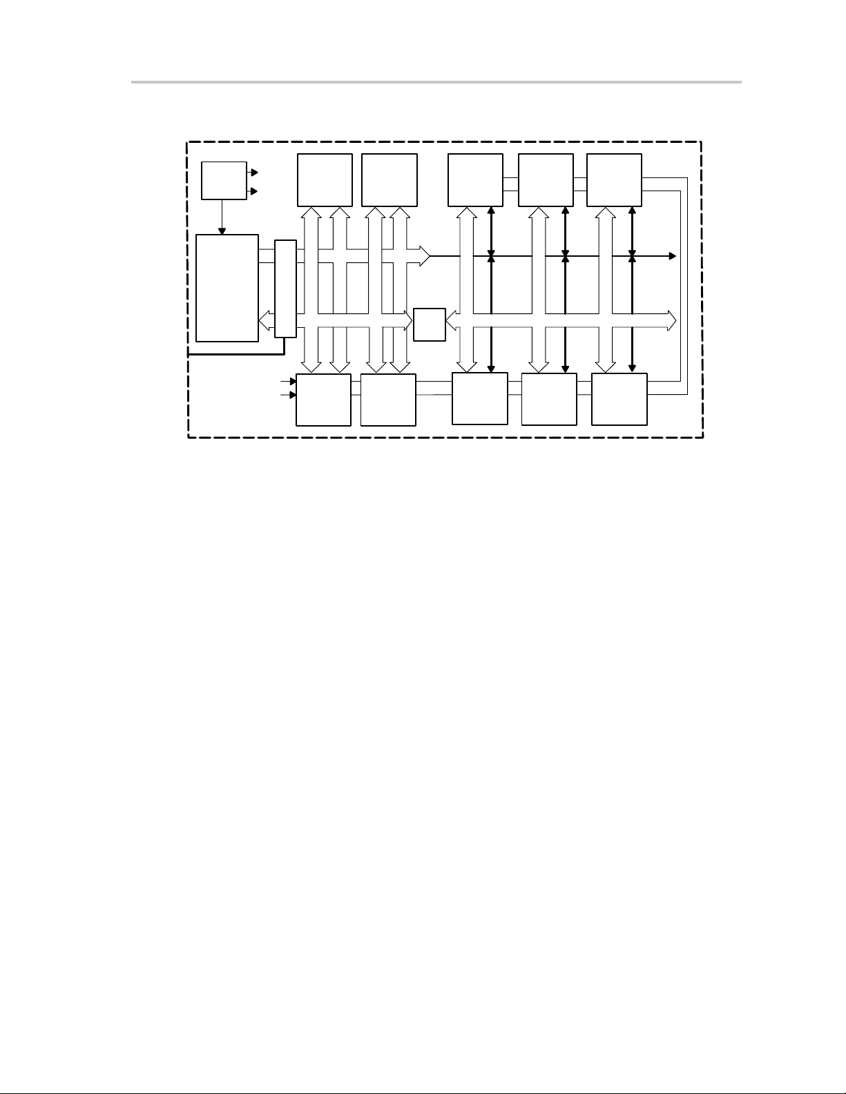
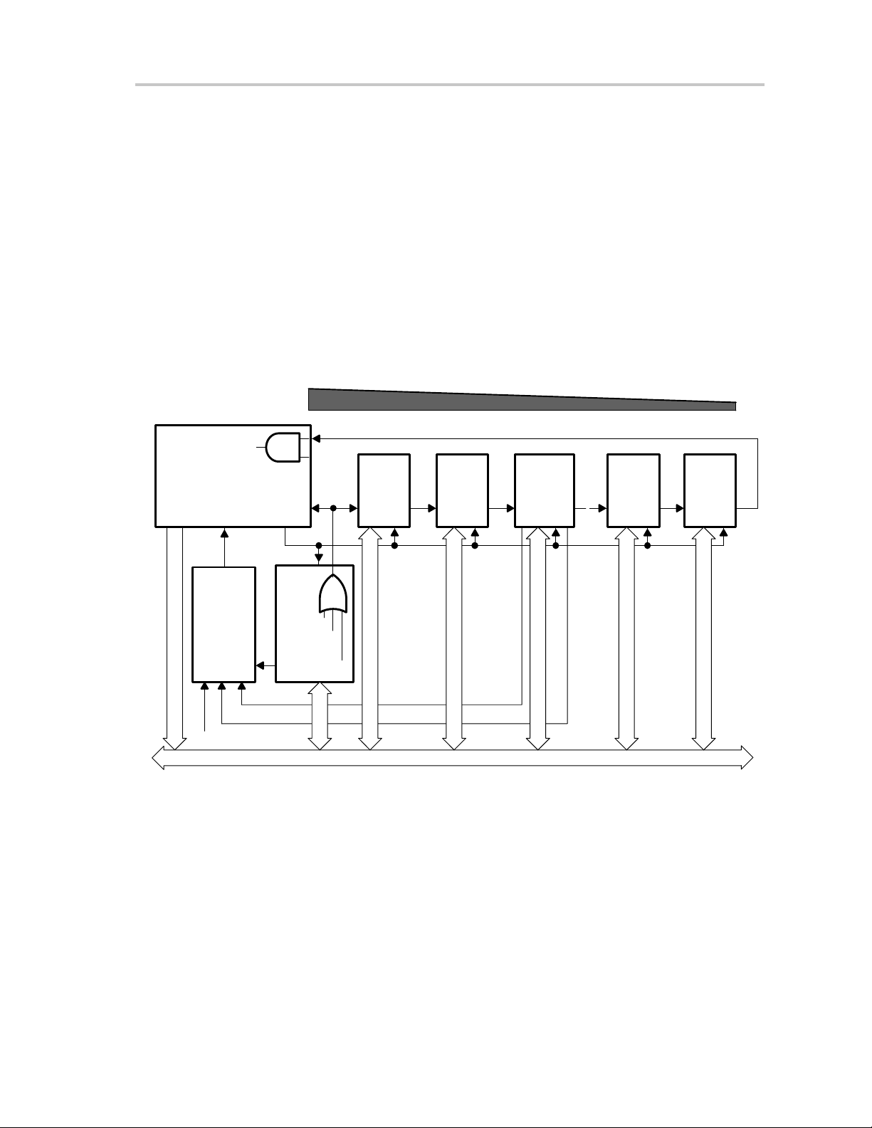
Figure 1−1.MSP430 Architecture
Embedded Emulation
MCLK
ACLK
SMCLK
ACLK
SMCLK
Flash/
ROM
MAB 16-Bit
JTAG/Debug
MDB 16-Bit
Watchdog
Clock
System
RISC CPU
16-Bit
JTAG
1.3 Embedded Emulation
Dedicated embedded emulation logic resides on the device itself and is
accessed via JTAG using no additional system resources.
RAM
Peripheral
Peripheral Peripheral Peripheral
Bus
Conv.
Peripheral
MDB 8-Bit
Peripheral Peripheral
The benefits of embedded emulation include:
- Unobtrusive development and debug with full-speed execution,
breakpoints, and single-steps in an application are supported.
- Development is in-system subject to the same characteristics as the final
application.
- Mixed-signal integrity is preserved and not subject to cabling interference.
1-3Introduction
Page 17

Address Space
1.4 Address Space
The MSP430 von-Neumann architecture has one address space shared with
special function registers (SFRs), peripherals, RAM, and Flash/ROM memory
as shown in Figure 1−2. See the device-specific data sheets for specific
memory maps. Code access are always performed on even addresses. Data
can be accessed as bytes or words.
The addressable memory space is 64 KB with future expansion planned.
Figure 1−2.Memory Map
Access
0FFFFh
0FFE0h
0FFDFh
0200h
01FFh
0100h
0FFh
010h
1.4.1 Flash/ROM
Word/Byte
Word/Byte
Word/Byte
Word
Byte
Byte
0Fh
0h
Interrupt Vector Table
Flash/ROM
RAM
16-Bit Peripheral Modules
8-Bit Peripheral Modules
Special Function Registers
The start address of Flash/ROM depends on the amount of Flash/ROM
present and varies by device. The end address for Flash/ROM is 0FFFFh.
Flash can be used for both code and data. Word or byte tables can be stored
and used in Flash/ROM without the need to copy the tables to RAM before
using them.
1.4.2 RAM
1-4 Introduction
The interrupt vector table is mapped into the upper 16 words of Flash/ROM
address space, with the highest priority interrupt vector at the highest
Flash/ROM word address (0FFFEh).
RAM starts at 0200h. The end address of RAM depends on the amount of RAM
present and varies by device. RAM can be used for both code and data.
Page 18
1.4.3 Peripheral Modules
Peripheral modules are mapped into the address space. The address space
from 0100 to 01FFh is reserved for 16-bit peripheral modules. These modules
should be accessed with word instructions. If byte instructions are used, only
even addresses are permissible, and the high byte of the result is always 0.
The address space from 010h to 0FFh is reserved for 8-bit peripheral modules.
These modules should be accessed with byte instructions. Read access of
byte modules using word instructions results in unpredictable data in the high
byte. If word data is written to a byte module only the low byte is written into
the peripheral register , ignoring the high byte.
1.4.4 Special Function Registers (SFRs)
Some peripheral functions are configured in the SFRs. The SFRs are located
in the lower 16 bytes of the address space, and are organized by byte. SFRs
must be accessed using byte instructions only. See the device-specific data
sheets for applicable SFR bits.
1.4.5 Memory Organization
Address Space
Bytes are located at even or odd addresses. Words are only located at even
addresses as shown in Figure 1−3. When using word instructions, only even
addresses may be used. The low byte of a word is always an even address.
The high byte is at the next odd address. For example, if a data word is located
at address xxx4h, then the low byte of that data word is located at address
xxx4h, and the high byte of that word is located at address xxx5h.
Figure 1−3.Bits, Bytes, and Words in a Byte-Organized Memory
xxxAh
157146. . Bits . .
. . Bits . .9180
Byte
Byte
Word (High Byte)
Word (Low Byte)
xxx9h
xxx8h
xxx7h
xxx6h
xxx5h
xxx4h
xxx3h
1-5Introduction
Page 19

Chapter 2
System Resets, Interrupts,
and Operating Modes
This chapter describes the MSP430x4xx system resets, interrupts, and
operating modes.
Topic Page
2.1 System Reset and Initialization 2-2. . . . . . . . . . . . . . . . . . . . . . . . . . . . . . . . .
2.2 Interrupts 2-5. . . . . . . . . . . . . . . . . . . . . . . . . . . . . . . . . . . . . . . . . . . . . . . . . . . . .
2.3 Operating Modes 2-13. . . . . . . . . . . . . . . . . . . . . . . . . . . . . . . . . . . . . . . . . . . . .
2.4 Principles for Low-Power Applications 2-16. . . . . . . . . . . . . . . . . . . . . . . . .
2.5 Connection of Unused Pins 2-16. . . . . . . . . . . . . . . . . . . . . . . . . . . . . . . . . . .
2-1System Resets, Interrupts, and Operating Modes
Page 20
System Reset and Initialization
2.1 System Reset and Initialization
The system reset circuitry shown in Figure 2−1 sources both a power-on reset
(POR) and a power-up clear (PUC) signal. Different events trigger these reset
signals and different initial conditions exist depending on which signal was
generated.
Figure 2−1.Power-On Reset and Power-Up Clear Schematic
V
CC
Brownout
Reset
0 V
0 V
SVS_POR
RST/NMI
WDTNMI
WDTSSEL
WDTIFG
† From watchdog timer peripheral module
†
†
†
WDTQn
†
†
EQU
KEYV
(from flash module)
~ 50us
Resetwd1
Resetwd2
S
R
S
S
S
S
R
POR
Latch
Delay
PUC
Latch
MCLK
POR
PUC
A POR is a device reset. A POR is only generated by the following three
events:
- Powering up the device
- A low signal on the RST/NMI pin when configured in the reset mode
- An SVS low condition when PORON = 1.
A PUC is always generated when a POR is generated, but a POR is not
generated by a PUC. The following events trigger a PUC:
- A POR signal
- Watchdog timer expiration when in watchdog mode only
- Watchdog timer security key violation
- A Flash memory security key violation
2-2 System Resets, Interrupts, and Operating Modes
Page 21
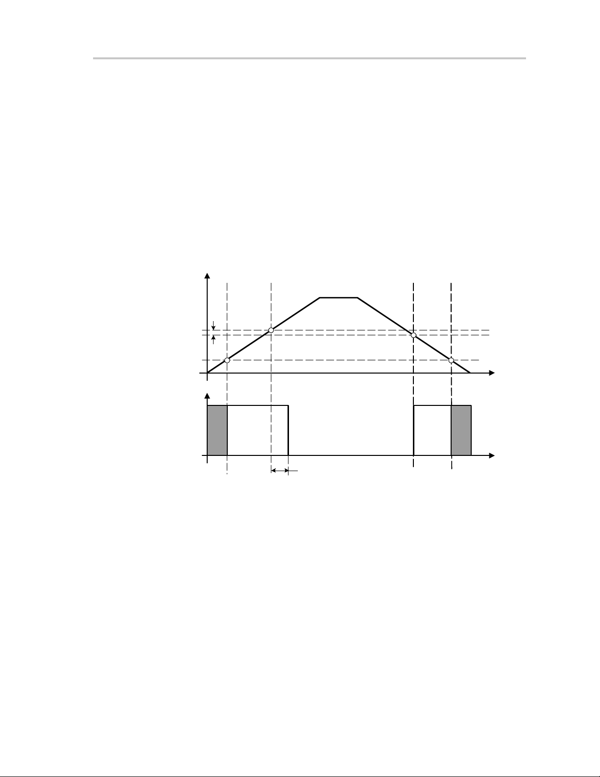
2.1.1 Brownout Reset (BOR)
All MSP430x4xx devices have a brownout reset circuit. The brownout reset
circuit detects low supply voltages such as when a supply voltage is applied
to or removed from the VCC terminal. The brownout reset circuit resets the
device by triggering a POR signal when power is applied or removed. The
operating levels are shown in Figure 2−2.
System Reset and Initialization
The POR signal becomes active when VCC crosses the V
remains active until VCC crosses the V
elapses. The delay t
hysteresis V
V
(B_IT−)
Figure 2−2.Brownout Timing
V
V
(B_IT+)
V
(B_IT−)
V
CC(start)
Set Signal for
POR circuitry
hys(B_IT−)
level. It
(BOR)
CC.
(BOR)
hys(B_ IT−)
CC(start)
threshold and the delay t
(B_IT+)
is adaptive being longer for a slow ramping V
ensures that the supply voltage must drop below
to generate another POR signal from the brownout reset circuitry.
V
CC
The
t
(BOR)
As the V
level is significantly above the V
(B_IT−)
level of the POR circuit,
(MIN)
the BOR provides a reset for power failures where VCC does not fall below
V
See device-specific datasheet for parameters.
(MIN).
2-3System Resets, Interrupts, and Operating Modes
Page 22

System Reset and Initialization
2.1.2 Device Initial Conditions After System Reset
After a POR, the initial MSP430 conditions are:
- The RST/NMI pin is configured in the reset mode.
- I/O pins are switched to input mode as described in the Digital I/O chapter.
- Other peripheral modules and registers are initialized as described in their
respective chapters in this manual.
- Status register (SR) is reset.
- The watchdog timer powers up active in watchdog mode.
- Program counter (PC) is loaded with address contained at reset vector
location (0FFFEh). CPU execution begins at that address.
Software Initialization
After a system reset, user software must initialize the MSP430 for the
application requirements. The following must occur:
- Initialize the SP, typically to the top of RAM.
- Initialize the watchdog to the requirements of the application.
- Configure peripheral modules to the requirements of the application.
Additionally, the watchdog timer, oscillator fault, and flash memory flags can
be evaluated to determine the source of the reset.
2-4 System Resets, Interrupts, and Operating Modes
Page 23
2.2 Interrupts
The interrupt priorities are fixed and defined by the arrangement of the
modules in the connection chain as shown in Figure 2−3. The nearer a module
is to the CPU/NMIRS, the higher the priority . Interrupt priorities determine what
interrupt is taken when more than one interrupt is pending simultaneously.
There are three types of interrupts:
- System reset
- (Non)-maskable NMI
- Maskable
Figure 2−3.Interrupt Priority
System Reset and Initialization
CPU
PUC
PUC
Circuit
WDT Security Key
Flash Security Key
Priority
GMIRS
GIE
NMIRS
OSCfault
Flash ACCV
Reset/NMI
MAB − 5LSBs
High
Module
1
Low
Module
2
12 12 12 12 1
Bus
Grant
WDT
Timer
Module
m
Module
n
2-5System Resets, Interrupts, and Operating Modes
Page 24

System Reset and Initialization
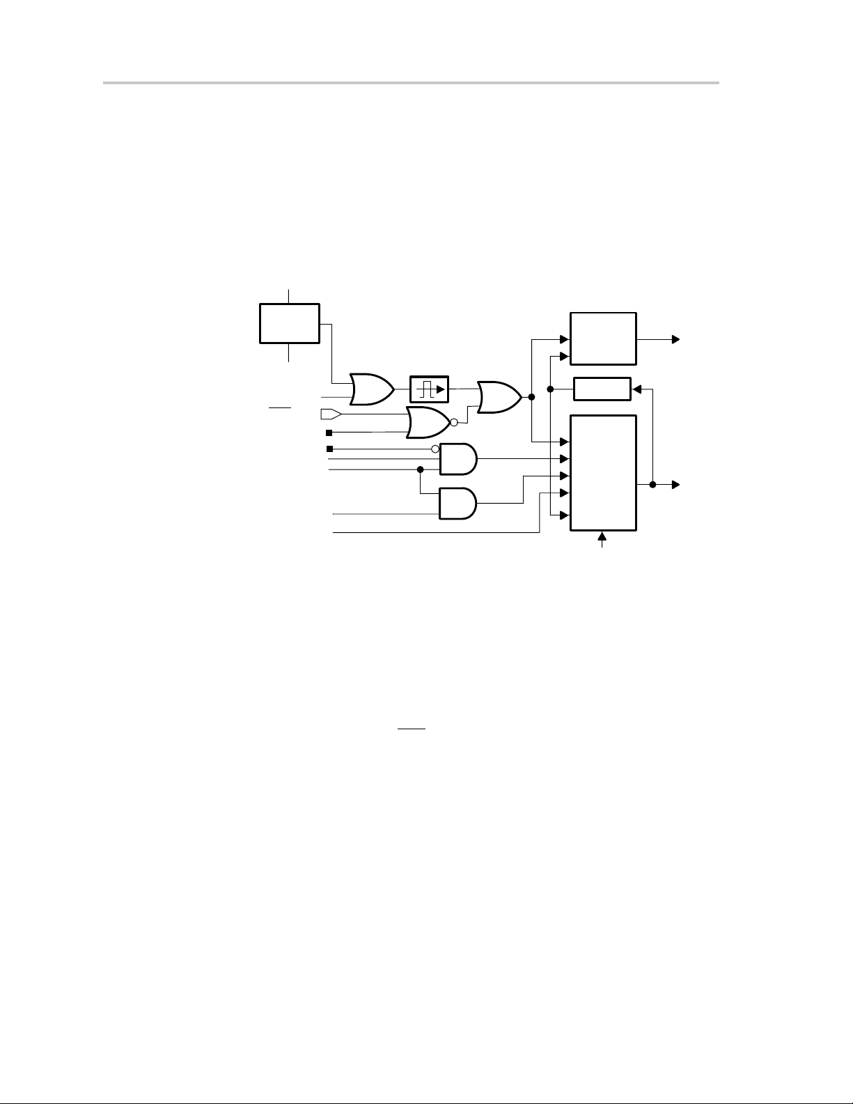
2.2.1 (Non)-Maskable Interrupts (NMI)
(Non)-maskable NMI interrupts are not masked by the general interrupt enable
bit (GIE), but are enabled by individual interrupt enable bits (ACCVIE, NMIIE,
OFIE). When a NMI interrupt is accepted, all NMI interrupt enable bits are
automatically reset. Program execution begins at the address stored in the
(non)-maskable interrupt vector, 0FFFCh. User software must set the required
NMI interrupt enable bits for the interrupt to be re-enabled. The block diagram
for NMI sources is shown in Figure 2−4.
A (non)-maskable NMI interrupt can be generated by three sources:
- An edge on the RST/NMI pin when configured in NMI mode
- An oscillator fault occurs
- An access violation to the flash memory
Reset/NMI Pin
At power-up, the RST/NMI pin is configured in the reset mode. The function
of the RST/NMI pins is selected in the watchdog control register WDTCTL. If
the RST/NMI pin is set to the reset function, the CPU is held in the reset state
as long as the RST/NMI pin is held low. After the input changes to a high state,
the CPU starts program execution at the word address stored in the reset
vector, 0FFFEh.
If the RST/NMI pin is configured by user software to the NMI function, a signal
edge selected by the WDTNMIES bit generates an NMI interrupt if the NMIIE
bit is set. The RST/NMI flag NMIIFG is also set.
Note: Holding RST/NMI Low
When configured in the NMI mode, a signal generating an NMI event should
not hold the RST/NMI pin low . If a PUC occurs from a different source while
the NMI signal is low, the device will be held in the reset state because a PUC
changes the RST/NMI pin to the reset function.
Note: Modifying WDTNMIES
When NMI mode is selected and the WDTNMIES bit is changed, an NMI can
be generated, depending on the actual level at the RST/NMI pin. When the
NMI edge select bit is changed before selecting the NMI mode, no NMI is
generated.
2-6 System Resets, Interrupts, and Operating Modes
Page 25
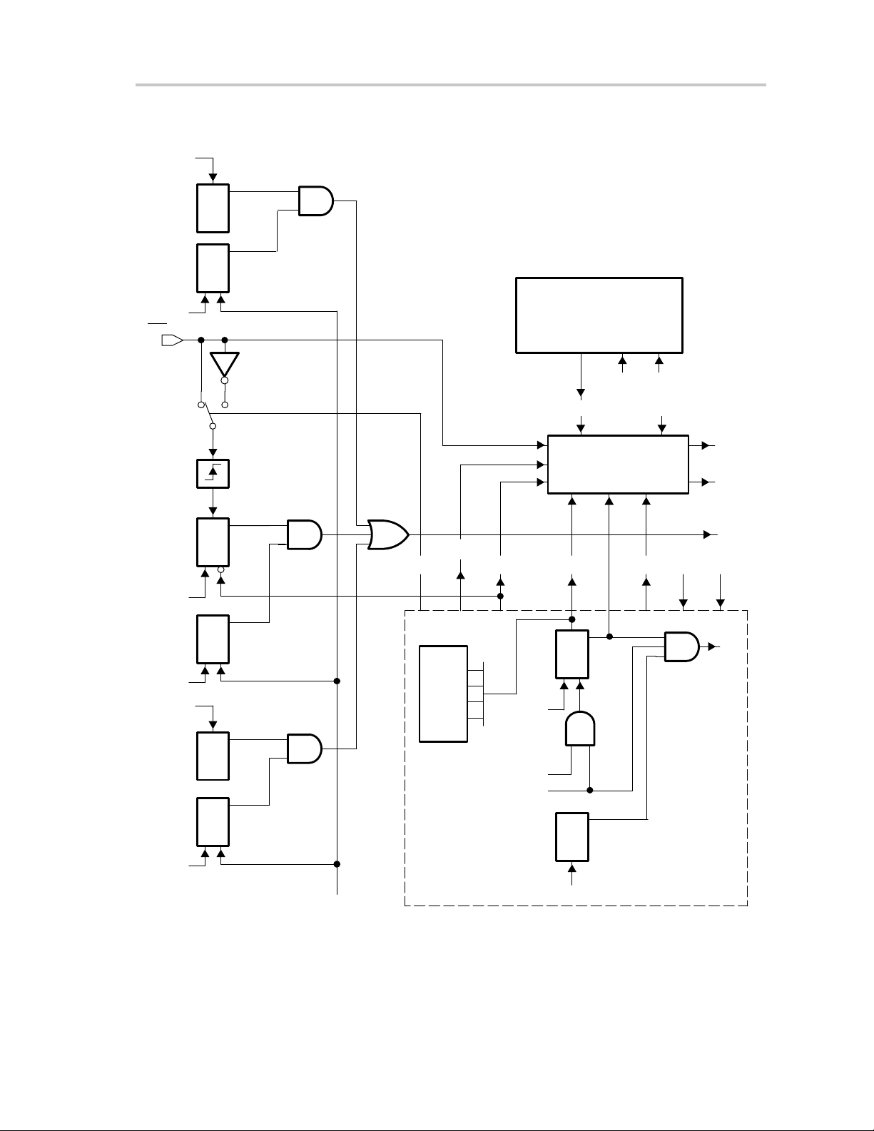
Figure 2−4.Block Diagram of (Non)-Maskable Interrupt Sources
ACCV
ACCVIFG
S
FCTL1.1
ACCVIE
IE1.5
Clear
System Reset and Initialization
PUC
RST/NMI
IFG1.4
PUC
IE1.4
PUC
OSCFault
IFG1.1
IE1.1
PUC
S
Clear
Clear
S
Clear
NMIIFG
NMIIE
OFIFG
OFIE
NMI_IRQA
WDTTMSEL
WDTNMIES
Counter
WDTNMI
WDT
WDTTMSEL
KEYV
WDTQn EQU
S
IFG1.0
Clear
POR
IRQA
IE1.0
Clear
Flash Module
POR PUC
System Reset
Generator
WDTIE
WDTIFG
V
CC
PUC POR
PUC
POR
NMIRS
IRQ
IRQA: Interrupt Request Accepted
Watchdog Timer Module
PUC
2-7System Resets, Interrupts, and Operating Modes
Page 26

System Reset and Initialization
Oscillator Fault
The oscillator fault signal warns of a possible error condition with the crystal
oscillator. The oscillator fault can be enabled to generate an NMI interrupt by
setting the OFIE bit. The OFIFG flag can then be tested by NMI the interrupt
service routine to determine if the NMI was caused by an oscillator fault.
A PUC signal can trigger an oscillator fault, because the PUC switches the
LFXT1 to LF mode, therefore switching of f the HF mode. The PUC signal also
switches off the XT2 oscillator.
Flash Access Violation
The flash ACCVIFG flag is set when a flash access violation occurs. The flash
access violation can be enabled to generate an NMI interrupt by setting the
ACCVIE bit. The ACCVIFG flag can then be tested by NMI the interrupt service
routine to determine if the NMI was caused by a flash access violation.
2-8 System Resets, Interrupts, and Operating Modes
Page 27
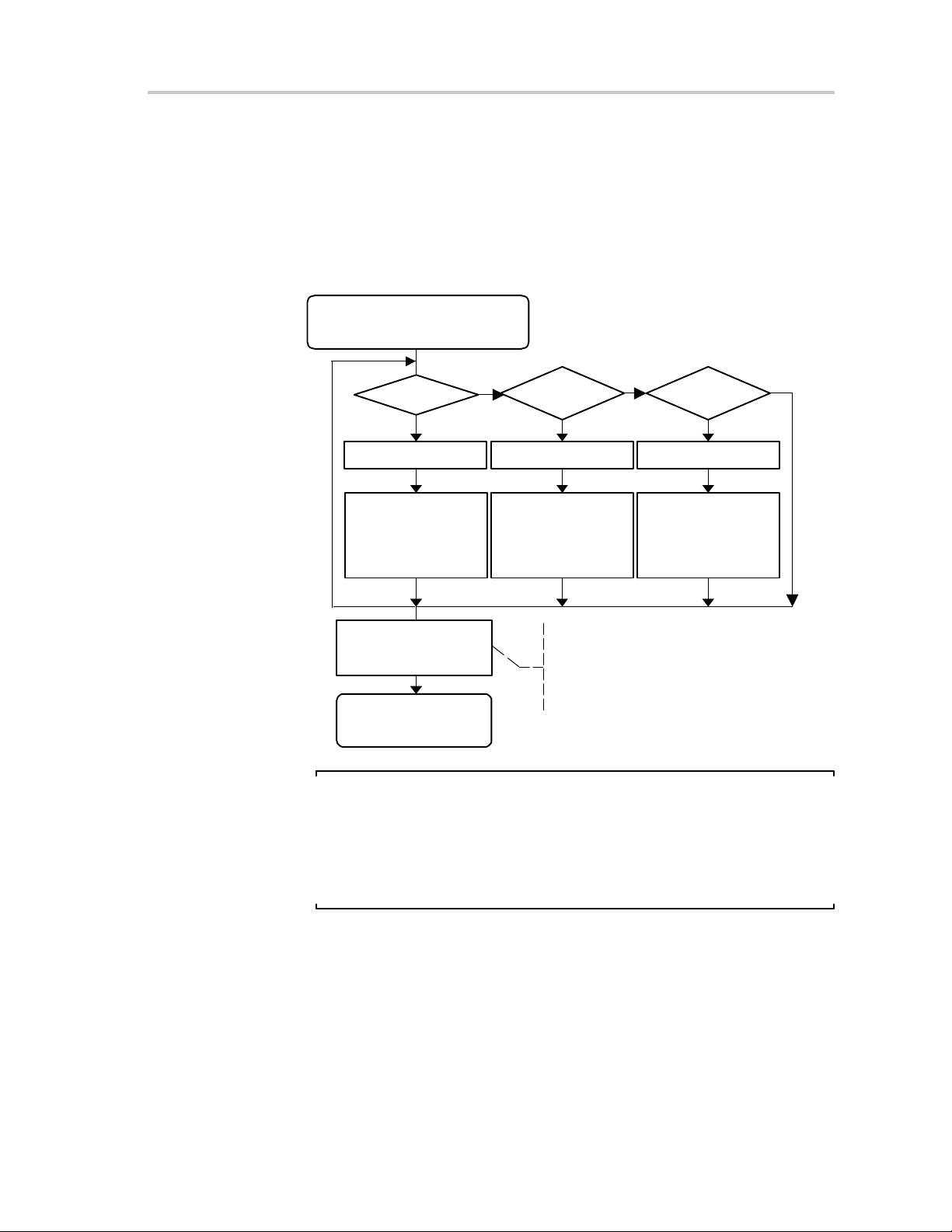
Example of an NMI Interrupt Handler
The NMI interrupt is a multiple-source interrupt. An NMI interrupt automatically
resets the NMIIE, OFIE and ACCVIE interrupt-enable bits. The user NMI
service routine resets the interrupt flags and re-enables the interrupt-enable
bits according to the application needs as shown in Figure 2−5.
Figure 2−5.NMI Interrupt Handler
Start of NMI Interrupt Handler
Reset by HW:
OFIE, NMIIE, ACCVIE
System Reset and Initialization
OFIFG=1
User’s Software,
Oscillator Fault
Handler
Optional
Set NMIIE, OFIE,
ACCVIE Within One
Instruction
RETI
End of NMI Interrupt
Handler
yes
no
ACCVIFG=1
yes
Reset ACCVIFG
User’s Software,
Flash Access
Violation Handler
Example 1:
BIS #(NMIIE+OFIE+ACCVIE), &IE1
Example 2:
BIS Mask,&IE1 ; Mask enables only
no
NMIIFG=1
yes
Reset NMIIFGReset OFIFG
User’s Software,
External NMI
Handler
; interrupt sources
no
Note: Enabling NMI Interrupts with ACCVIE, NMIIE, and OFIE
Care should be taken when the ACCVIE, NMIIE, and OFIE enable bits are
set inside of an NMI interrupt service routine. This re-enables the interrupt
and can cause stack overflow if the interrupt flag has become set, due to
nested interrupts. When set inside of an NMI service routine, they should be
set by the last instruction of the routine before the RETI instruction.
2.2.2 Maskable Interrupts
Maskable interrupts are caused by peripherals with interrupt capability
including the watchdog timer overflow in interval-timer mode. Each maskable
interrupt source can be disabled individually by an interrupt enable bit, or all
maskable interrupts can be disabled by the general interrupt enable (GIE) bit
in the status register (SR).
2-9System Resets, Interrupts, and Operating Modes
Page 28
System Reset and Initialization
Each individual peripheral interrupt is discussed in the associated peripheral
module chapter in this manual.
2.2.3 Interrupt Processing
When an interrupt is requested from a peripheral and the peripheral interrupt
enable bit and GIE bit are set, the interrupt service routine is requested. Only
the individual enable bit must be set for (non)-maskable interrupts to be
requested.
Interrupt Acceptance
The interrupt latency is 6 cycles, starting with the acceptance of an interrupt
request, and lasting until the start of execution of the first instruction of the
interrupt-service routine, as shown in Figure 2−6. The interrupt logic executes
the following:
1) Any currently executing instruction is completed.
2) The PC, which points to the next instruction, is pushed onto the stack.
3) The SR is pushed onto the stack.
4) The interrupt with the highest priority is selected if multiple interrupts
occurred during the last instruction and are pending for service.
5) The interrupt request flag resets automatically on single-source flags.
Multiple source flags remain set for servicing by software.
6) The SR is cleared with the exception of SCG0, which is left unchanged.
This terminates any low-power mode. Because the GIE bit is cleared,
further interrupts are disabled.
7) The content of the interrupt vector is loaded into the PC: the program
continues with the interrupt service routine at that address.
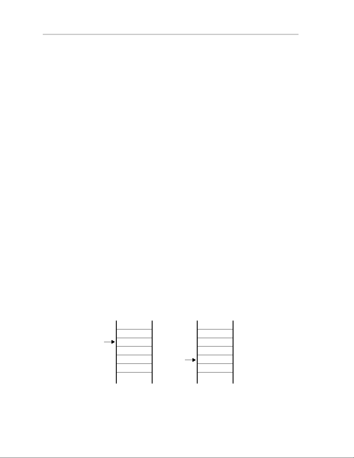
Figure 2−6.Interrupt Processing
Before
Interrupt
Item1
SP TOS
Item2
After
Interrupt
Item1
Item2
PC
SP TOS
SR
2-10 System Resets, Interrupts, and Operating Modes
Page 29
Return From Interrupt
The interrupt handling routine terminates with the instruction:
RETI (return from an interrupt service routine)
The return from the interrupt takes 5 cycles to execute the following actions
and is illustrated in Figure 2−7.
1) The SR with all previous settings pops from the stack. All previous settings
of GIE, CPUOFF, etc. are now in effect, regardless of the settings used
during the interrupt service routine.
2) The PC pops from the stack and begins execution at the point where it was
interrupted.
Figure 2−7.Return From Interrupt
Before After
System Reset and Initialization
Return From Interrupt
Item1
Item2
PC
SP TOS
SR
SP TOS
Item1
Item2
PC
SR
Interrupt nesting is enabled if the GIE bit is set inside an interrupt service
routine. When interrupt nesting is enabled, any interrupt occurring during an
interrupt service routine will interrupt the routine, regardless of the interrupt
priorities.
2-11System Resets, Interrupts, and Operating Modes
Page 30

System Reset and Initialization
2.2.4 Interrupt Vectors
The interrupt vectors and the power-up starting address are located in the
address range 0FFFFh − 0FFE0h as described in Table 2−1. A vector is
programmed by the user with the 16-bit address of the corresponding interrupt
service routine. See the device-specific data sheet for the complete interrupt
vector list.
Table 2−1.Interrupt Sources,Flags, and Vectors
INTERRUPT SOURCE
Power-up, external
reset, watchdog,
flash password
NMI, oscillator fault,
flash memory access
violation
device-specific 0FFFAh 13
device-specific 0FFF8h 12
device-specific 0FFF6h 11
Watchdog timer WDTIFG maskable 0FFF4h 10
device-specific 0FFF2h 9
device-specific 0FFF0h 8
device-specific 0FFEEh 7
device-specific 0FFECh 6
device-specific 0FFEAh 5
device-specific 0FFE8h 4
device-specific 0FFE6h 3
device-specific 0FFE4h 2
device-specific 0FFE2h 1
device-specific
INTERRUPT
FLAG
WDTIFG
KEYV
NMIIFG
OFIFG
ACCVIFG
SYSTEM
INTERRUPT
Reset 0FFFEh 15, highest
(non)-maskable
(non)-maskable
(non)-maskable
WORD
ADDRESS
0FFFCh 14
0FFE0h 0, lowest
PRIORITY
2.2.5 Special Function Registers (SFRs)
Some module enable bits, interrupt enable bits, and interrupt flags are located
in the SFRs. The SFRs are located in the lower address range and are
implemented in byte format. SFRs must be accessed using byte instructions.
See the device-specific datasheet for the SFR configuration.
2-12 System Resets, Interrupts, and Operating Modes
Page 31

2.3 Operating Modes
The MSP430 family is designed for ultralow-power applications and uses
different operating modes shown in Figure 2−9.
The operating modes take into account three different needs:
- Ultralow-power
- Speed and data throughput
- Minimization of individual peripheral current consumption
The MSP430 typical current consumption is shown in Figure 2−8.
Figure 2−8.Typical Current Consumption of 41x Devices vs Operating Modes
Operating Modes
90
45
300
200
55
32
17
0
AM
LPM0 LPM2 LPM3 LPM4
11
Operating Modes
0.9
0.7
VCC = 3 V
VCC = 2.2 V
0.1 0.1
A @ 1 MHzµ
ICC/
315
270
225
180
135
The low-power modes 0−4 are configured with the CPUOFF , OSCOFF, SCG0,
and SCG1 bits in the status register The advantage of including the CPUOFF,
OSCOFF, SCG0, and SCG1 mode-control bits in the status register is that the
present operating mode is saved onto the stack during an interrupt service
routine. Program flow returns to the previous operating mode if the saved SR
value is not altered during the interrupt service routine. Program flow can be
returned to a d i fferent operating mode by manipulating the saved SR value on
the stack inside of the interrupt service routine. The mode-control bits and the
stack can be accessed with any instruction.
When setting any of the mode-control bits, the selected operating mode takes
effect immediately. Peripherals operating with any disabled clock are disabled
until the clock becomes active. The peripherals may also be disabled with their
individual control register settings. All I/O port pins and RAM/registers are
unchanged. Wake up is possible through all enabled interrupts.
2-13System Resets, Interrupts, and Operating Modes
Page 32

Operating Modes
Figure 2−9.MSP430x4xx Operating Modes For Basic Clock System
WDT Active,
Time Expired, Overflow
WDT Active,
Security Key Violation
CPUOFF = 1
SCG0 = 0
SCG1 = 0
LPM0
CPU Off, FLL+ On,
MCLK On, ACLK On
CPUOFF = 1
SCG0 = 1
SCG1 = 0
LPM1
CPU Off, FLL+ Off,
MCLK On, ACLK On
RST/NMI
Reset Active
WDTIFG = 1
WDTIFG = 1
Active Mode
CPU Is Active
Peripheral Modules Are Active
CPUOFF = 1
SCG0 = 0
SCG1 = 1
LPM2
CPU Off, FLL+ Off,
MCLK Off, ACLK On
POR
WDTIFG = 0
PUC
CPUOFF = 1
VCC On
RST/NMI is Reset Pin
WDT is Active
CPUOFF = 1
OSCOFF = 1
SCG0 = 1
SCG1 = 1
CPU Off, FLL+ Off,
MCLK Off, ACLK On
DC Generator Off
RST/NMI
NMI Active
SCG0 = 1
SCG1 = 1
LPM4
CPU Off, FLL+ Off,
MCLK Off, ACLK Off
DC Generator Off
LPM3
SCG1 SCG0 OSCOFF CPUOFF Mode CPU and Clocks Status
0 0 0 0 Active CPU is active, all enabled clocks are active
0 0 0 1 LPM0 CPU, MCLK are disabled
SMCLK , ACLK are active
0 1 0 1 LPM1 CPU, MCLK, DCO osc. are disabled
DC generator is disabled if the DCO is not used for
MCLK or SMCLK in active mode
SMCLK , ACLK are active
1 0 0 1 LPM2 CPU, MCLK, SMCLK, DCO osc. are disabled
DC generator remains enabled
ACLK is active
1 1 0 1 LPM3 CPU, MCLK, SMCLK, DCO osc. are disabled
DC generator disabled
ACLK is active
1
1 1 1 LPM4 CPU and all clocks disabled
2-14 System Resets, Interrupts, and Operating Modes
Page 33

2.3.1 Entering and Exiting Low-Power Modes
An enabled interrupt event wakes the MSP430 from any of the low-power
operating modes. The program flow is:
- Enter interrupt service routine:
J The PC and SR are stored on the stack
J The CPUOFF, SCG1, and OSCOFF bits are automatically reset
- Options for returning from the interrupt service routine:
J The original SR is popped from the stack, restoring the previous
operating mode.
J The SR bits stored on the stack can be modified within the interrupt
service routine returning to a different operating mode when the RETI
instruction is executed.
; Enter LPM0 Example
BIS #GIE+CPUOFF,SR ; Enter LPM0
; ... ; Program stops here
;
; Exit LPM0 Interrupt Service Routine
BIC #CPUOFF,0(SP) ; Exit LPM0 on RETI
RETI
Operating Modes
; Enter LPM3 Example
BIS #GIE+CPUOFF+SCG1+SCG0,SR ; Enter LPM3
; ... ; Program stops here
;
; Exit LPM3 Interrupt Service Routine
BIC #CPUOFF+SCG1+SCG0,0(SP) ; Exit LPM3 on RETI
RETI
Extended Time in Low-Power Modes
The negative temperature coefficient of the DCO should be considered when
the DCO is disabled for extended low-power mode periods. If the temperature
changes significantly, the DCO frequency at wake-up may be significantly
different from when the low-power mode was entered and may be out of the
specified operating range. To avoid this, the DCO can be set to it lowest value
before entering the low-power mode for extended periods of time where
temperature can change.
; Enter LPM4 Example with lowest DCO Setting
BIC.B #FN_8+FN_4+FN_3+FN_2,&SCFI0 ; Lowest Range
MOV.B #010h,&SCFI1 ; Select Tap 2
BIS #GIE+CPUOFF+OSCOFF+SCG1+SCG0,SR ; Enter LPM4
; ... ; Program stops
; Interrupt Service Routine
BIC #CPUOFF+OSCOFF+SCG1+SCG0,0(SR); Exit LPM4 on RETI
RETI
2-15System Resets, Interrupts, and Operating Modes
Page 34

Principles for Low-Power Applications
2.4 Principles for Low-Power Applications
Often, the most important factor for reducing power consumption is using the
MSP430’s clock system to maximize the time in LPM3. LPM3 power
consumption is less than 2 µA typical with both a real-time clock function and
all interrupts active. A 32-kHz watch crystal is used for the ACLK and the CPU
is clocked from the DCO (normally off) which has a 6-µs wake-up.
- Use interrupts to wake the processor and control program flow.
- Peripherals should be switched on only when needed.
- Use low-power integrated peripheral modules in place of software driven
functions. For example Timer_A and Timer_B can automatically generate
PWM and capture external timing, with no CPU resources.
- Calculated branching and fast table look-ups should be used in place of
flag polling and long software calculations.
- Avoid frequent subroutine and function calls due to overhead.
- For longer software routines, single-cycle CPU registers should be used.
2.5 Connection of Unused Pins
The correct termination of all unused pins is listed in Table 2−2.
Table 2−2.Connection of Unused Pins
Pin Potential Comment
AV
CC
AV
SS
V
REF+
Ve
REF+
V
/Ve
REF−
XIN DV
XOUT Open
XT2IN DV
XT2OUT Open 43x and 44x devices
Px.0 to Px.7 Open Switched to port function, output direction
RST
/NMI DVCC or V
R03 DV
COM0 Open
TDO Open
TDI Open
TMS Open
TCK Open
Sxx
REF−
DV
DV
Open
DV
DV
Open
CC
SS
SS
SS
CC
SS
SS
43x and 44x devices
47 kΩ pullup with 10nF pull down
CC
2-16 System Resets, Interrupts, and Operating Modes
Page 35

Chapter 3
This chapter describes the MSP430 CPU, addressing modes, and instruction
set.
Topic Page
3.1 CPU Introduction 3-2. . . . . . . . . . . . . . . . . . . . . . . . . . . . . . . . . . . . . . . . . . . . . .
3.2 CPU Registers 3-4. . . . . . . . . . . . . . . . . . . . . . . . . . . . . . . . . . . . . . . . . . . . . . . .
3.3 Addressing Modes 3-9. . . . . . . . . . . . . . . . . . . . . . . . . . . . . . . . . . . . . . . . . . . .
3.4 Instruction Set 3-17. . . . . . . . . . . . . . . . . . . . . . . . . . . . . . . . . . . . . . . . . . . . . . .
3-1RISC 16-Bit CPU
Page 36

CPU Introduction
3.1 CPU Introduction
The CPU incorporates features specifically designed for modern
programming techniques such as calculated branching, table processing and
the use of high-level languages such as C. The CPU can address the complete
address range without paging.
The CPU features include:
- RISC architecture with 27 instructions and 7 addressing modes.
- Orthogonal architecture with every instruction usable with every
- Full register access including program counter, status registers, and stack
- Single-cycle register operations.
- Large 16-bit register file reduces fetches to memory.
- 16-bit address bus allows direct access and branching throughout entire
addressing mode.
pointer.
memory range.
- 16-bit data bus allows direct manipulation of word-wide arguments.
- Constant generator provides six most used immediate values and
reduces code size.
- Direct memory-to-memory transfers without intermediate register holding.
- Word and byte addressing and instruction formats.
The block diagram of the CPU is shown in Figure 3−1.
3-2 RISC 16-Bit CPU
Page 37

Figure 3−1.CPU Block Diagram
MDB − Memory Data Bus Memory Address Bus −MAB
CPU Introduction
015
R0/PC Program Counter 0
R1/SP Stack Pointer
R2/SR/CG1 Status
R3/CG2 Constant Generator
R4 General Purpose
R5 General Purpose
R6 General Purpose
R7 General Purpose
R8 General Purpose
R9 General Purpose
R10 General Purpose
R11 General Purpose
R12 General Purpose
R13 General Purpose
0
16
Zero, Z
Carry, C
Overflow, V
Negative, N
R14 General Purpose
R15 General Purpose
dst src
16−bit ALU
16
MCLK
3-3RISC 16-Bit CPU
Page 38

CPU Registers
3.2 CPU Registers
The CPU incorporates sixteen 16-bit registers. R0, R1, R2 and R3 have
dedicated functions. R4 to R15 are working registers for general use.
3.2.1 Program Counter (PC)
The 16-bit program counter (PC/R0) points to the next instruction to be
executed. Each instruction uses an even number of bytes (two, four, or six),
and the PC is incremented accordingly. Instruction accesses in the 64-KB
address space are performed on word boundaries, and the PC is aligned to
even addresses. Figure 3−2 shows the program counter .
Figure 3−2.Program Counter
15 0
1
Program Counter Bits 15 to 1
0
The PC can be addressed with all instructions and addressing modes. A few
examples:
MOV #LABEL,PC ; Branch to address LABEL
MOV LABEL,PC ; Branch to address contained in LABEL
MOV @R14,PC ; Branch indirect to address in R14
3-4 RISC 16-Bit CPU
Page 39

3.2.2 Stack Pointer (SP)
The stack pointer (SP/R1) is used by the CPU to store the return addresses
of subroutine calls and interrupts. It uses a predecrement, postincrement
scheme. In addition, the SP can be used by software with all instructions and
addressing modes. Figure 3−3 shows the SP. The SP is initialized into RAM
by the user, and is aligned to even addresses.
Figure 3−4 shows stack usage.
Figure 3−3.Stack Pointer
15 0
CPU Registers
1
Figure 3−4.Stack Usage
0xxxh
0xxxh − 2
0xxxh − 4
0xxxh − 6
0xxxh − 8
The special cases of using the SP as an argument to the PUSH and POP
instructions are described and shown in Figure 3−5.
Stack Pointer Bits 15 to 1
MOV 2(SP),R6 ; Item I2 −> R6
MOV R7,0(SP) ; Overwrite TOS with R7
PUSH #0123h ; Put 0123h onto TOS
POP R8 ; R8 = 0123h
SP
POP R8Address
I1
I2
I3
0123h
PUSH #0123h
I1
I2
I3
SP
I1
I2
I3
0123h
0
SP
Figure 3−5.PUSH SP - POP SP Sequence
PUSH SP
SP
old
SP
SP
1
The stack pointer is changed after
a PUSH SP instruction.
1
POP SP
SP
2
The stack pointer is not changed after a POP SP
instruction. The POP SP instruction places SP1 into the
stack pointer SP (SP2=SP1)
1SP
3-5RISC 16-Bit CPU
Page 40

CPU Registers
3.2.3 Status Register (SR)
The status register (SR/R2), used as a source or destination register, can be
used in the register mode only addressed with word instructions. The remaining combinations of addressing modes are used to support the constant generator. Figure 3 −6 shows the SR bits.
Figure 3−6.Status Register Bits
15 0
Reserved
Table 3−1 describes the status register bits.
Table 3−1.Description of Status Register Bits
Bit Description
V Overflow bit. This bit is set when the result of an arithmetic operation
overflows the signed-variable range.
ADD(.B),ADDC(.B) Set when:
SUB(.B),SUBC(.B),CMP(.B) Set when:
SCG1 System clock generator 1. This bit, when set, turns off the DCO dc
generator, if DCOCLK is not used for MCLK or SMCLK.
SCG0 System clock generator 0. This bit, when set, turns off the FLL+ loop
control
OSCOFF Oscillator Off. This bit, when set, turns off the LFXT1 crystal oscillator,
when LFXT1CLK is not use for MCLK or SMCLK
CPUOFF CPU off. This bit, when set, turns off the CPU.
GIE General interrupt enable. This bit, when set, enables maskable
interrupts. When reset, all maskable interrupts are disabled.
N Negative bit. This bit is set when the result of a byte or word operation
is negative and cleared when the result is not negative.
Word operation: N is set to the value of bit 15 of the
Byte operation: N is set to the value of bit 7 of the
Z Zero bit. This bit is set when the result of a byte or word operation is 0
and cleared when the result is not 0.
C
Carry bit. This bit is set when the result of a byte or word operation
produced a carry and cleared when no carry occurred.
879
CPU
OSC
SCG1V
SCG0 GIE Z C
Positive + Positive = Negative
Negative + Negative = Positive,
otherwise reset
Positive − Negative = Negative
Negative − Positive = Positive,
otherwise reset
result
result
OFF
OFF
N
3-6 RISC 16-Bit CPU
Page 41

3.2.4 Constant Generator Registers CG1 and CG2
Six commonly-used constants are generated with the constant generator
registers R2 and R3, without requiring an additional 16-bit word of program
code. The constants are selected with the source-register addressing modes
(As), as described in Table 3−2.
Table 3−2.Values of Constant Generators CG1, CG2
Register As Constant Remarks
R2 00 − − − − − Register mode
R2 01 (0) Absolute address mode
R2 10 00004h +4, bit processing
R2 11 00008h +8, bit processing
R3 00 00000h 0, word processing
R3 01 00001h +1
R3 10 00002h +2, bit processing
R3 11 0FFFFh −1, word processing
The constant generator advantages are:
CPU Registers
- No special instructions required
- No additional code word for the six constants
- No code memory access required to retrieve the constant
The assembler uses the constant generator automatically if one of the six
constants is used as an immediate source operand. Registers R2 and R3,
used in the constant mode, cannot be addressed explicitly; they act as
source-only registers.
Constant Generator − Expanded Instruction Set
The RISC instruction set of the MSP430 has only 27 instructions. However, the
constant generator allows the MSP430 assembler to support 24 additional,
emulated instructions. For example, the single-operand instruction:
CLR dst
is emulated by the double-operand instruction with the same length:
MOV R3,dst
where the #0 is replaced by the assembler, and R3 is used with As=00.
INC dst
is replaced by:
ADD 0(R3),dst
3-7RISC 16-Bit CPU
Page 42

CPU Registers
3.2.5 General−Purpose Registers R4 - R15
The twelve registers, R4−R15, are general-purpose registers. All of these
registers can be used as data registers, address pointers, or index values and
can be accessed with byte or word instructions as shown in Figure 3−7.
Figure 3−7.Register-Byte/Byte-Register Operations
Register-Byte Operation
High Byte Low Byte
Unused
Byte
Example Register-Byte Operation Example Byte-Register Operation
R5 = 0A28Fh R5 = 01202h
R6 = 0203h R6 = 0223h
Mem(0203h) = 012h Mem(0223h) = 05Fh
ADD.B R5,0(R6) ADD.B @R6,R5
08Fh 05Fh
+ 012h + 002h
0A1h 00061h
Mem (0203h) = 0A1h R5 = 00061h
C = 0, Z = 0, N = 1 C = 0, Z = 0, N = 0
Register
Memory
Byte-Register Operation
High Byte Low Byte
Byte
0h
Memory
Register
+ (Addressed byte) + (Low byte of register)
−>(Addressed byte) −>(Low byte of register, zero to High byte)
3-8 RISC 16-Bit CPU
(Low byte of register) (Addressed byte)
Page 43

3.3 Addressing Modes
Seven addressing modes for the source operand and four addressing modes
for the destination operand can address the complete address space with no
exceptions. The bit numbers in Table 3−3 describe the contents of the As
(source) and Ad (destination) mode bits.
Table 3−3.Source/Destination Operand Addressing Modes
As/Ad Addressing Mode Syntax Description
00/0 Register mode Rn Register contents are operand
01/1 Indexed mode X(Rn) (Rn + X) points to the operand. X
01/1 Symbolic mode ADDR (PC + X) points to the operand. X
01/1 Absolute mode &ADDR The word following the instruction
10/− Indirect register
mode
11/− Indirect
autoincrement
11/−
Immediate mode #N The word following the instruction
@Rn Rn is used as a pointer to the
@Rn+ Rn is used as a pointer to the
Addressing Modes
is stored in the next word.
is stored in the next word. Indexed
mode X(PC) is used.
contains the absolute address. X
is stored in the next word. Indexed
mode X(SR) is used.
operand.
operand. Rn is incremented
afterwards by 1 for .B instructions
and by 2 for .W instructions.
contains the immediate constant
N. Indirect autoincrement mode
@PC+ is used.
The seven addressing modes are explained in detail in the following sections.
Most of the examples show the same addressing mode for the source and
destination, but any valid combination of source and destination addressing
modes is possible in an instruction.
Note: Use of Labels EDE, TONI, TOM, and LEO
Throughout MSP430 documentation EDE, TONI, TOM, and LEO are used
as generic labels. They are only labels. They have no special meaning.
3-9RISC 16-Bit CPU
Page 44

Addressing Modes
3.3.1 Register Mode
The register mode is described in Table 3−4.
Table 3−4.Register Mode Description
Assembler Code Content of ROM
MOV R10,R11 MOV R10,R11
Length: One or two words
Operation: Move the content of R10 to R11. R10 is not affected.
Comment: Valid for source and destination
Example: MOV R10,R11
Before: After:
R11
PC
0A023hR10
0FA15h
PC
old
R11
PC PC
0A023hR10
0A023h
old
+ 2
Note: Data in Registers
The data in the register can be accessed using word or byte instructions. If
byte instructions are used, the high byte is always 0 in the result. The status
bits are handled according to the result of the byte instruction.
3-10 RISC 16-Bit CPU
Page 45

3.3.2 Indexed Mode
The indexed mode is described in Table 3−5.
Table 3−5.Indexed Mode Description
Assembler Code Content of ROM
MOV 2(R5),6(R6) MOV X(R5),Y(R6)
Length: T wo or three words
Operation: Move the contents of the source address (contents of R5 + 2)
Comment: Valid for source and destination
Addressing Modes
X = 2
Y = 6
to the destination address (contents of R6 + 6). The source
and destination registers (R5 and R6) are not affected. In
indexed mode, the program counter is incremented
automatically so that program execution continues with the
next instruction.
Example: MOV 2(R5),6(R6);
Before:
0FF16h
0FF14h
0FF12h
01094h
01092h
01090h
01084h
01082h
01080h
Address
Space
00006h
00002h
04596h PC
0xxxxh
05555h
0xxxxh
0xxxxh
01234h
0xxxxh
Register
R5
R6
01080h
0108Ch
0108Ch
+0006h
01092h
01080h
+0002h
01082h
After:
0FF16h
0FF14h
0FF12h
01094h
01092h
01090h
01084h
01082h
01080h
Address
Space
0xxxxh
00006h
00002h
04596h
0xxxxh
01234h
0xxxxh
0xxxxh
01234h
0xxxxh
PC
Register
R5
R6
01080h
0108Ch
3-11RISC 16-Bit CPU
Page 46

Addressing Modes
3.3.3 Symbolic Mode
The symbolic mode is described in Table 3−6.
Table 3−6.Symbolic Mode Description
Assembler Code Content of ROM
MOV EDE,TONI MOV X(PC),Y(PC)
Length: T wo or three words
Operation: Move the contents of the source address EDE (contents of
X = EDE − PC
Y = TONI − PC
PC + X) to the destination address TONI (contents of PC + Y).
The words after the instruction contain the differences
between the PC and the source or destination addresses.
The assembler computes and inserts offsets X and Y
automatically. With symbolic mode, the program counter (PC)
is incremented automatically so that program execution
continues with the next instruction.
Comment: Valid for source and destination
Example: MOV EDE,TONI ;Source address EDE = 0F016h
;Dest. address TONI=01114h
Before:
0FF16h
0FF14h
0FF12h
0F018h
0F016h
0F014h
01116h
01114h
01112h
Address
Space
011FEh
0F102h
04090h PC
0xxxxh
0A123h
0xxxxh
0xxxxh
05555h
0xxxxh
Register
0FF14h
+0F102h
0F016h
0FF16h
+011FEh
01114h
After:
0FF16h
0FF14h
0FF12h
0F018h
0F016h
0F014h
01116h
01114h
01112h
Address
Space
0xxxxh
011FEh
0F102h
04090h
0xxxxh
0A123h
0xxxxh
0xxxxh
0A123h
0xxxxh
Register
PC
3-12 RISC 16-Bit CPU
Page 47

3.3.4 Absolute Mode
The absolute mode is described in Table 3−7.
Table 3−7.Absolute Mode Description
Assembler Code Content of ROM
MOV &EDE,&TONI MOV X(0),Y(0)
Length: T wo or three words
Operation: Move the contents of the source address EDE to the
Comment: Valid for source and destination
Example: MOV &EDE,&TONI ;Source address EDE=0F016h,
Addressing Modes
X = EDE
Y = TONI
destination address TONI. The words after the instruction
contain the absolute address of the source and destination
addresses. With absolute mode, the PC is incremented
automatically so that program execution continues with the
next instruction.
;dest. address TONI=01114h
Before:
0FF16h
0FF14h
0FF12h
0F018h
0F016h
0F014h
01116h
01114h
01112h
Address
Space
01114h
0F016h
04292h PC
0xxxxh
0A123h
0xxxxh
0xxxxh
01234h
0xxxxh
Register
After:
0FF16h
0FF14h
0FF12h
0F018h
0F016h
0F014h
01116h
01114h
01112h
Address
Space
0xxxxh
01114h
0F016h
04292h
0xxxxh
0A123h
0xxxxh
0xxxxh
0A123h
0xxxxh
Register
PC
This address mode is mainly for hardware peripheral modules that are located
at an absolute, fixed address. These are addressed with absolute mode to
ensure software transportability (for example, position-independent code).
3-13RISC 16-Bit CPU
Page 48

Addressing Modes
3.3.5 Indirect Register Mode
The indirect register mode is described in Table 3−8.
Table 3−8.Indirect Mode Description
Assembler Code Content of ROM
MOV @R10,0(R11) MOV @R10,0(R11)
Length: One or two words
Operation: Move the contents of the source address (contents of R10) to
Comment: Valid only for source operand. The substitute for destination
Example: MOV.B @R10,0(R11)
the destination address (contents of R11). The registers are
not modified.
operand is 0(Rd).
Before:
0FF16h
0FF14h
0FF12h
0FA34h
0FA32h
0FA30h
002A8h
002A7h
002A6h
Address
Space
0xxxxh
0000h
04AEBh
0xxxxh
0xxxxh
05BC1h
0xxxxh
0xxh
012h
0xxh
PC
R10
R11
Register
0FA33h
002A7h
After:
0FF16h
0FF14h
0FF12h
0FA34h
0FA32h
0FA30h
002A8h
002A7h
002A6h
Address
Space
0xxxxh
0000h
04AEBh
0xxxxh
0xxxxh
05BC1h
0xxxxh
0xxh
05Bh
0xxh
PC
R10
R11
Register
0FA33h
002A7h
3-14 RISC 16-Bit CPU
Page 49

3.3.6 Indirect Autoincrement Mode
The indirect autoincrement mode is described in Table 3−9.
Table 3−9.Indirect Autoincrement Mode Description
Assembler Code Content of ROM
MOV @R10+,0(R11) MOV @R10+,0(R11)
Length: One or two words
Operation: Move the contents of the source address (contents of R10) to
the destination address (contents of R11). Register R10 is
incremented by 1 for a byte operation, or 2 for a word
operation after the fetch; it points to the next address without
any overhead. This is useful for table processing.
Comment: Valid only for source operand. The substitute for destination
operand is 0(Rd) plus second instruction INCD Rd.
Example: MOV @R10+,0(R11)
Addressing Modes
Before:
0FF18h
0FF16h
0FF14h
0FF12h
0FA34h
0FA32h
0FA30h
010AAh
010A8h
010A6h
Address
Space
0xxxxh
00000h
04ABBh
0xxxxh
0xxxxh
05BC1h
0xxxxh
0xxxxh
01234h
0xxxxh
PC
R10
R11
Register
0FA32h
010A8h
After:
0FF18h
0FF16h
0FF14h
0FF12h
0FA34h
0FA32h
0FA30h
010AAh
010A8h
010A6h
Address
Space
0xxxxh
00000h
04ABBh
0xxxxh
0xxxxh
05BC1h
0xxxxh
0xxxxh
05BC1h
0xxxxh
PC
R11
Register
0FA34hR10
010A8h
The autoincrementing of the register contents occurs after the operand is
fetched. This is shown in Figure 3−8.
Figure 3−8.Operand Fetch Operation
Instruction Address Operand
+1/ +2
3-15RISC 16-Bit CPU
Page 50

Addressing Modes
3.3.7 Immediate Mode
The immediate mode is described in Table 3−10.
Table 3−10.Immediate Mode Description
Assembler Code Content of ROM
MOV #45h,TONI MOV @PC+,X(PC)
Length: T wo or three words
It is one word less if a constant of CG1 or CG2 can be used.
Operation: Move the immediate constant 45h, which is contained in the
word following the instruction, to destination address TONI.
When fetching the source, the program counter points to the
word following the instruction and moves the contents to the
destination.
Comment: Valid only for a source operand.
45
X = TONI − PC
Example: MOV #45h,TONI
Before:
0FF16h
0FF14h
0FF12h
010AAh
010A8h
010A6h
Address
Space
01192h
00045h
040B0h PC
0xxxxh
01234h
0xxxxh
Register
0FF16h
+01192h
010A8h
After:
0FF18h
0FF16h
0FF14h
0FF12h
010A8h
010A6h
Address
Space
0xxxxh
01192h
00045h
040B0h
0xxxxh010AAh
00045h
0xxxxh
Register
PC
3-16 RISC 16-Bit CPU
Page 51

3.4 Instruction Set
Instruction Set
The complete MSP430 instruction set consists of 27 core instructions and 24
emulated instructions. The core instructions are instructions that have unique
op-codes decoded by the CPU. The emulated instructions are instructions that
make code easier to write and read, but do not have op-codes themselves,
instead they are replaced automatically by the assembler with an equivalent
core instruction. There is no code or performance penalty for using emulated
instruction.
There are three core-instruction formats:
- Dual-operand
- Single-operand
- Jump
All single-operand and dual-operand instructions can be byte or word
instructions by using .B or .W extensions. Byte instructions are used to access
byte data or byte peripherals. Word instructions are used to access word data
or word peripherals. If no extension is used, the instruction is a word
instruction.
The source and destination of an instruction are defined by the following fields:
src The source operand defined by As and S-reg
dst The destination operand defined by Ad and D-reg
As The addressing bits responsible for the addressing mode used
for the source (src)
S-reg The working register used for the source (src)
Ad The addressing bits responsible for the addressing mode used
for the destination (dst)
D-reg The working register used for the destination (dst)
B/W Byte or word operation:
0: word operation
1: byte operation
Note: Destination Address
Destination addresses are valid anywhere in the memory map. However,
when using an instruction that modifies the contents of the destination, the
user must ensure the destination address is writable. For example, a
masked-ROM location would be a valid destination address, but the contents
are not modifiable, so the results of the instruction would be lost.
3-17RISC 16-Bit CPU
Page 52

Instruction Set
3.4.1 Double-Operand (Format I) Instructions
Figure 3−9 illustrates the double-operand instruction format.
Figure 3−9.Double Operand Instruction Format
15 0
Op-code
Table 3−11 lists and describes the double operand instructions.
Table 3−11.Double Operand Instructions
Mnemonic S-Reg,
D-Reg
MOV(.B)
ADD(.B) src,dst src + dst → dst ****
ADDC(.B) src,dst src + dst + C → dst ** **
SUB(.B) src,dst dst + .not.src + 1 → dst ****
SUBC(.B) src,dst dst + .not.src + C → dst ****
CMP(.B) src,dst dst − src ****
DADD(.B) src,dst src + dst + C → dst (decimally) * * * *
BIT(.B) src,dst src .and. dst 0 * * *
BIC(.B) src,dst .not.src .and. dst → dst −−−−
BIS(.B) src,dst src .or. dst → dst −−−−
XOR(.B) src,dst src .xor. dst → dst ** **
AND(.B)
src,dst src → dst − − − −
src,dst src .and. dst → dst 0 * * *
8714 13 12 11 10 9 6 5 4 3 2 1
B/W D-Reg
AdS-Reg
Operation Status Bits
As
VNZC
* The status bit is affected
− The status bit is not affected
0 The status bit is cleared
1 The status bit is set
Note: Instructions CMP and SUB
The instructions CMP and SUB are identical except for the storage of the
result. The same is true for the BIT and AND instructions.
3-18 RISC 16-Bit CPU
Page 53

3.4.2 Single-Operand (Format II) Instructions
Figure 3−10 illustrates the single-operand instruction format.
Figure 3−10. Single Operand Instruction Format
Instruction Set
15 0
Table 3−12 lists and describes the single operand instructions.
Table 3−12.Single Operand Instructions
Mnemonic
RRC(.B)
RRA(.B) dst MSB → MSB →....LSB → C0***
PUSH(.B) src SP − 2
SWPB dst Swap bytes −−−−
CALL dst SP − 2 → SP, PC+2 → @SP −−−−
RETI TOS
SXT
S-Reg,
D-Reg
dst C → MSB →.......LSB → C * * * *
dst Bit 7 → Bit 8........Bit 15 0 * * *
Op-code
8714 13 12 11 10 9 6 5 4 3 2 1
B/W D/S-Reg
Operation Status Bits
→ SP, src → @SP −−−−
→ PC
dst
→ SR, SP + 2 → SP ****
TOS
→ PC,SP + 2 → SP
Ad
VNZC
* The status bit is affected
− The status bit is not affected
0 The status bit is cleared
1 The status bit is set
All addressing modes are possible for the CALL instruction. If the symbolic
mode (ADDRESS), the immediate mode (#N), the absolute mode (&EDE) or
the indexed mode x(RN) is used, the word that follows contains the address
information.
3-19RISC 16-Bit CPU
Page 54

Instruction Set
3.4.3 Jumps
Figure 3−11 shows the conditional-jump instruction format.
Figure 3−11. Jump Instruction Format
15 0
Op-code
Table 3−13 lists and describes the jump instructions.
Table 3−13.Jump Instructions
Mnemonic S-Reg, D-Reg Operation
JEQ/JZ Label Jump to label if zero bit is set
JNE/JNZ Label Jump to label if zero bit is reset
JC Label Jump to label if carry bit is set
JNC Label Jump to label if carry bit is reset
JN Label Jump to label if negative bit is set
JGE Label Jump to label if (N .XOR. V) = 0
JL Label Jump to label if (N .XOR. V) = 1
JMP
Conditional jumps support program branching relative to the PC and do not
affect the status bits. The possible jump range is from −511 to +512 words
relative to the PC value at the jump instruction. The 10-bit program-counter
offset is treated as a signed 10-bit value that is doubled and added to the
program counter:
8714 13 12 11 10 9 6 5 4 3 2 1
C 10-Bit PC Offset
Label Jump to label unconditionally
3-20 RISC 16-Bit CPU
PC
new
= PC
+ 2 + PC
old
offset
× 2
Page 55

Instruction Set
ADC[.W] Add carry to destination
ADC.B Add carry to destination
Syntax ADC dst or ADC.W dst
ADC.B dst
Operation dst + C −> dst
Emulation ADDC #0,dst
ADDC.B #0,dst
Description The carry bit (C) is added to the destination operand. The previous contents
of the destination are lost.
Status Bits N: Set if result is negative, reset if positive
Z: Set if result is zero, reset otherwise
C: Set if dst was incremented from 0FFFFh to 0000, reset otherwise
Set if dst was incremented from 0FFh to 00, reset otherwise
V: Set if an arithmetic overflow occurs, otherwise reset
Mode Bits OSCOFF, CPUOFF, and GIE are not affected.
Example The 16-bit counter pointed to by R13 is added to a 32-bit counter pointed to
by R12.
ADD @R13,0(R12) ; Add LSDs
ADC 2(R12) ; Add carry to MSD
Example The 8-bit counter pointed to by R13 is added to a 16-bit counter pointed to by
R12.
ADD.B @R13,0(R12) ; Add LSDs
ADC.B 1(R12) ; Add carry to MSD
RISC 16−Bit CPU
3-21
Page 56

Instruction Set
ADD[.W] Add source to destination
ADD.B Add source to destination
Syntax ADD src,dst or ADD.W src,dst
ADD.B src,dst
Operation src + dst −> dst
Description The source operand is added to the destination operand. The source operand
is not affected. The previous contents of the destination are lost.
Status Bits N: Set if result is negative, reset if positive
Z: Set if result is zero, reset otherwise
C: Set if there is a carry from the result, cleared if not
V: Set if an arithmetic overflow occurs, otherwise reset
Mode Bits OSCOFF, CPUOFF, and GIE are not affected.
Example R5 is increased by 10. The jump to TONI is performed on a carry.
ADD #10,R5
JC TONI ; Carry occurred
...... ; No carry
Example R5 is increased by 10. The jump to TONI is performed on a carry.
ADD.B #10,R5 ; Add 10 to Lowbyte of R5
JC TONI ; Carry occurred, if (R5) ≥ 246 [0Ah+0F6h]
...... ; No carry
3-22
RISC 16−Bit CPU
Page 57

Instruction Set
ADDC[.W] Add source and carry to destination
ADDC.B Add source and carry to destination
Syntax ADDC src,dst or ADDC.W src,dst
ADDC.B src,dst
Operation src + dst + C −> dst
Description The source operand and the carry bit (C) are added to the destination operand.
The source operand is not affected. The previous contents of the destination
are lost.
Status Bits N: Set if result is negative, reset if positive
Z: Set if result is zero, reset otherwise
C: Set if there is a carry from the MSB of the result, reset otherwise
V: Set if an arithmetic overflow occurs, otherwise reset
Mode Bits OSCOFF, CPUOFF, and GIE are not affected.
Example The 32-bit counter pointed to by R13 is added to a 32-bit counter , eleven words
(20/2 + 2/2) above the pointer in R13.
ADD @R13+,20(R13) ; ADD LSDs with no carry in
ADDC @R13+,20(R13) ; ADD MSDs with carry
... ; resulting from the LSDs
Example The 24-bit counter pointed to by R13 is added to a 24-bit counter , eleven words
above the pointer in R13.
ADD.B @R13+,10(R13) ; ADD LSDs with no carry in
ADDC.B @R13+,10(R13) ; ADD medium Bits with carry
ADDC.B @R13+,10(R13) ; ADD MSDs with carry
... ; resulting from the LSDs
RISC 16−Bit CPU
3-23
Page 58

Instruction Set
AND[.W] Source AND destination
AND.B Source AND destination
Syntax AND src,dst or AND.W src,dst
AND.B src,dst
Operation src .AND. dst −> dst
Description The source operand and the destination operand are logically ANDed. The
result is placed into the destination.
Status Bits N: Set if result MSB is set, reset if not set
Z: Set if result is zero, reset otherwise
C: Set if result is not zero, reset otherwise ( = .NOT. Zero)
V: Reset
Mode Bits OSCOFF, CPUOFF, and GIE are not affected.
Example The bits set in R5 are used as a mask (#0AA55h) for the word addressed by
TOM. If the result is zero, a branch is taken to label TONI.
MOV #0AA55h,R5 ; Load mask into register R5
AND R5,TOM ; mask word addressed by TOM with R5
JZ TONI ;
...... ; Result is not zero
;
;
;or
;
;
AND #0AA55h,TOM
JZ TONI
Example The bits of mask #0A5h are logically ANDed with the low byte TOM. If the result
is zero, a branch is taken to label TONI.
AND.B #0A5h,TOM ; mask Lowbyte TOM with 0A5h
JZ TONI ;
...... ; Result is not zero
3-24
RISC 16−Bit CPU
Page 59

Instruction Set
BIC[.W] Clear bits in destination
BIC.B Clear bits in destination
Syntax BIC src,dst or BIC.W src,dst
BIC.B src,dst
Operation .NOT.src .AND. dst −> dst
Description The inverted source operand and the destination operand are logically
ANDed. The result is placed into the destination. The source operand is not
affected.
Status Bits Status bits are not affected.
Mode Bits OSCOFF, CPUOFF, and GIE are not affected.
Example The six MSBs of the RAM word LEO are cleared.
BIC #0FC00h,LEO ; Clear 6 MSBs in MEM(LEO)
Example The five MSBs of the RAM byte LEO are cleared.
BIC.B #0F8h,LEO ; Clear 5 MSBs in Ram location LEO
RISC 16−Bit CPU
3-25
Page 60

Instruction Set
BIS[.W] Set bits in destination
BIS.B Set bits in destination
Syntax BIS src,dst or BIS.W src,dst
BIS.B src,dst
Operation src .OR. dst −> dst
Description The source operand and the destination operand are logically ORed. The
result is placed into the destination. The source operand is not affected.
Status Bits Status bits are not affected.
Mode Bits OSCOFF, CPUOFF, and GIE are not affected.
Example The six LSBs of the RAM word TOM are set.
BIS #003Fh,TOM; set the six LSBs in RAM location TOM
Example The three MSBs of RAM byte TOM are set.
BIS.B #0E0h,TOM ; set the 3 MSBs in RAM location TOM
3-26
RISC 16−Bit CPU
Page 61

Instruction Set
BIT[.W] Test bits in destination
BIT.B Test bits in destination
Syntax BIT src,dst or BIT.W src,dst
Operation src .AND. dst
Description The source and destination operands are logically ANDed. The result affects
only the status bits. The source and destination operands are not affected.
Status Bits N: Set if MSB of result is set, reset otherwise
Z: Set if result is zero, reset otherwise
C: Set if result is not zero, reset otherwise (.NOT. Zero)
V: Reset
Mode Bits OSCOFF, CPUOFF, and GIE are not affected.
Example If bit 9 of R8 is set, a branch is taken to label TOM.
BIT #0200h,R8 ; bit 9 of R8 set?
JNZ TOM ; Yes, branch to TOM
... ; No, proceed
Example If bit 3 of R8 is set, a branch is taken to label TOM.
BIT.B #8,R8
JC TOM
Example A serial communication receive bit (RCV) is tested. Because the carry bit is
equal to the state of the tested bit while using the BIT instruction to test a single
bit, the carry bit is used by the subsequent instruction; the read information is
shifted into register RECBUF.
;
; Serial communication with LSB is shifted first:
; xxxx xxxx xxxx xxxx
BIT.B #RCV,RCCTL ; Bit info into carry
RRC RECBUF ; Carry −> MSB of RECBUF
; cxxx xxxx
...... ; repeat previous two instructions
...... ; 8 times
; cccc cccc
; ^ ^
; MSB LSB
; Serial communication with MSB shifted first:
BIT.B #RCV,RCCTL ; Bit info into carry
RLC.B RECBUF ; Carry −> LSB of RECBUF
; xxxx xxxc
...... ; repeat previous two instructions
...... ; 8 times
; cccc cccc
; | LSB
; MSB
RISC 16−Bit CPU
3-27
Page 62

Instruction Set
* BR, BRANCH Branch to .......... destination
Syntax BR dst
Operation dst −> PC
Emulation MOV dst,PC
Description An unconditional branch is taken to an address anywhere in the 64K address
space. All source addressing modes can be used. The branch instruction is
a word instruction.
Status Bits Status bits are not affected.
Example Examples for all addressing modes are given.
BR #EXEC ;Branch to label EXEC or direct branch (e.g. #0A4h)
; Core instruction MOV @PC+,PC
BR EXEC ; Branch to the address contained in EXEC
; Core instruction MOV X(PC),PC
; Indirect address
BR &EXEC ; Branch to the address contained in absolute
; address EXEC
; Core instruction MOV X(0),PC
; Indirect address
BR R5 ; Branch to the address contained in R5
; Core instruction MOV R5,PC
; Indirect R5
BR @R5 ; Branch to the address contained in the word
; pointed to by R5.
; Core instruction MOV @R5,PC
; Indirect, indirect R5
BR @R5+ ; Branch to the address contained in the word pointed
; to by R5 and increment pointer in R5 afterwards.
; The next time—S/W flow uses R5 pointer—it can
; alter program execution due to access to
; next address in a table pointed to by R5
; Core instruction MOV @R5,PC
; Indirect, indirect R5 with autoincrement
BR X(R5) ; Branch to the address contained in the address
; pointed to by R5 + X (e.g. table with address
; starting at X). X can be an address or a label
; Core instruction MOV X(R5),PC
; Indirect, indirect R5 + X
3-28
RISC 16−Bit CPU
Page 63

Instruction Set
CALL Subroutine
Syntax CALL dst
Operation dst −> tmp dst is evaluated and stored
SP − 2 −> SP
PC −> @SP PC updated to TOS
tmp −> PC dst saved to PC
Description A subroutine call is made to an address anywhere in the 64K address space.
All addressing modes can be used. The return address (the address of the
following instruction) is stored on the stack. The call instruction is a word
instruction.
Status Bits Status bits are not affected.
Example Examples for all addressing modes are given.
CALL #EXEC ; Call on l a b e l EXEC or immediate address (e.g. #0A4h)
; SP−2 → SP, PC+2 → @SP, @PC+ → PC
CALL EXEC ; Call on the address contained in EXEC
; SP−2 → SP, PC+2 → @SP, X(PC) → PC
; Indirect address
CALL &EXEC ; Call on the address contained in absolute address
; EXEC
; SP−2 → SP, PC+2 → @SP, X(0) → PC
; Indirect address
CALL R5 ; Call on the address contained in R5
; SP−2 → SP, PC+2 → @SP, R5 → PC
; Indirect R5
CALL @R5 ; Call on the address contained in the word
; pointed to by R5
; SP−2 → SP, PC+2 → @SP, @R5 → PC
; Indirect, indirect R5
CALL @R5+ ; Call on the address contained in the word
; pointed to by R5 and increment pointer in R5.
; The next time—S/W flow uses R5 pointer—
; it can alter the program execution due to
; access to next address in a table pointed to by R5
; SP−2 → SP, PC+2 → @SP, @R5 → PC
; Indirect, indirect R5 with autoincrement
CALL X(R5) ; Call on the address contained in the address pointed
; to by R5 + X (e.g. table with address starting at X)
; X can be an address or a label
; SP−2 → SP, PC+2 → @SP, X(R5) → PC
; Indirect, indirect R5 + X
RISC 16−Bit CPU
3-29
Page 64

Instruction Set
* CLR[.W] Clear destination
* CLR.B Clear destination
Syntax CLR dst or CLR.W dst
CLR.B dst
Operation 0 −> dst
Emulation MOV #0,dst
MOV.B #0,dst
Description The destination operand is cleared.
Status Bits Status bits are not affected.
Example RAM word TONI is cleared.
CLR TONI ; 0 −> TONI
Example Register R5 is cleared.
CLR R5
Example RAM byte TONI is cleared.
CLR.B TONI ; 0 −> TONI
3-30
RISC 16−Bit CPU
Page 65

Instruction Set
* CLRC Clear carry bit
Syntax CLRC
Operation 0 −> C
Emulation BIC #1,SR
Description The carry bit (C) is cleared. The clear carry instruction is a word instruction.
Status Bits N: Not affected
Z: Not affected
C: Cleared
V: Not affected
Mode Bits OSCOFF, CPUOFF, and GIE are not affected.
Example The 16-bit decimal counter pointed to by R13 is added to a 32-bit counter
pointed to by R12.
CLRC ; C=0: defines start
DADD @R13,0(R12) ; add 16-bit counter to low word of 32-bit counter
DADC 2(R12) ; add carry to high word of 32-bit counter
RISC 16−Bit CPU
3-31
Page 66

Instruction Set
* CLRN Clear negative bit
Syntax CLRN
Operation 0 → N
or
(.NOT.src .AND. dst −> dst)
Emulation BIC #4,SR
Description The constant 04h is inverted (0FFFBh) and is logically ANDed with the
destination operand. The result is placed into the destination. The clear
negative bit instruction is a word instruction.
Status Bits N: Reset to 0
Z: Not affected
C: Not affected
V: Not affected
Mode Bits OSCOFF, CPUOFF, and GIE are not affected.
Example The Negative bit in the status register is cleared. This avoids special treatment
with negative numbers of the subroutine called.
CLRN
CALL SUBR
......
......
SUBR JN SUBRET ; If input is negative: do nothing and return
......
......
......
SUBRET RET
3-32
RISC 16−Bit CPU
Page 67

Instruction Set
* CLRZ Clear zero bit
Syntax CLRZ
Operation 0 → Z
or
(.NOT.src .AND. dst −> dst)
Emulation BIC #2,SR
Description The constant 02h is inverted (0FFFDh) and logically ANDed with the
destination operand. The result is placed into the destination. The clear zero
bit instruction is a word instruction.
Status Bits N: Not affected
Z: Reset to 0
C: Not affected
V: Not affected
Mode Bits OSCOFF, CPUOFF, and GIE are not affected.
Example The zero bit in the status register is cleared.
CLRZ
RISC 16−Bit CPU
3-33
Page 68

Instruction Set
CMP[.W] Compare source and destination
CMP.B Compare source and destination
Syntax CMP src,dst or CMP.W src,dst
CMP.B src,dst
Operation dst + .NOT .src + 1
or
(dst − src)
Description The source operand is subtracted from the destination operand. This is
accomplished by adding the 1s complement of the source operand plus 1. The
two operands are not affected and the result is not stored; only the status bits
are affected.
Status Bits N: Set if result is negative, reset if positive (src >= dst)
Z: Set if result is zero, reset otherwise (src = dst)
C: Set if there is a carry from the MSB of the result, reset otherwise
V: Set if an arithmetic overflow occurs, otherwise reset
Mode Bits OSCOFF, CPUOFF, and GIE are not affected.
Example R5 and R6 are compared. If they are equal, the program continues at the label
EQUAL.
CMP R5,R6 ; R5 = R6?
JEQ EQUAL ; YES, JUMP
Example Two RAM blocks are compared. If they are not equal, the program branches
to the label ERROR.
MOV #NUM,R5 ; number of words to be compared
MOV #BLOCK1,R6 ; BLOCK1 start address in R6
MOV #BLOCK2,R7 ; BLOCK2 start address in R7
L$1 CMP @R6+,0(R7) ; Are Words equal? R6 increments
JNZ ERROR ; No, branch to ERROR
INCD R7 ; Increment R7 pointer
DEC R5 ; Are all words compared?
JNZ L$1 ; No, another compare
Example The RAM bytes addressed by EDE and TONI are compared. If they are equal,
the program continues at the label EQUAL.
CMP.B EDE,TONI ; MEM(EDE) = MEM(TONI)?
JEQ EQUAL ; YES, JUMP
3-34
RISC 16−Bit CPU
Page 69

Instruction Set
* DADC[.W] Add carry decimally to destination
* DADC.B Add carry decimally to destination
Syntax DADC dst or DADC.W src,dst
DADC.B dst
Operation dst + C −> dst (decimally)
Emulation DADD #0,dst
DADD.B #0,dst
Description The carry bit (C) is added decimally to the destination.
Status Bits N: Set if MSB is 1
Z: Set if dst is 0, reset otherwise
C: Set if destination increments from 9999 to 0000, reset otherwise
Set if destination increments from 99 to 00, reset otherwise
V: Undefined
Mode Bits OSCOFF, CPUOFF, and GIE are not affected.
Example The four-digit decimal number contained in R5 is added to an eight-digit deci-
mal number pointed to by R8.
CLRC ; Reset carry
; next instruction’s start condition is defined
DADD R5,0(R8) ; Add LSDs + C
DADC 2(R8) ; Add carry to MSD
Example The two-digit decimal number contained in R5 is added to a four-digit decimal
number pointed to by R8.
CLRC ; Reset carry
; next instruction’s start condition is defined
DADD.B R5,0(R8) ; Add LSDs + C
DADC 1(R8) ; Add carry to MSDs
RISC 16−Bit CPU
3-35
Page 70

Instruction Set
DADD[.W] Source and carry added decimally to destination
DADD.B Source and carry added decimally to destination
Syntax DADD src,dst or DADD.W src,dst
DADD.B src,dst
Operation src + dst + C −> dst (decimally)
Description The source operand and the destination operand are treated as four binary
coded decimals (BCD) with positive signs. The source operand and the carry
bit (C) are added decimally to the destination operand. The source operand
is not affected. The previous contents of the destination are lost. The result is
not defined for non-BCD numbers.
Status Bits N: Set if the MSB is 1, reset otherwise
Z: Set if result is zero, reset otherwise
C: Set if the result is greater than 9999
Set if the result is greater than 99
V: Undefined
Mode Bits OSCOFF, CPUOFF, and GIE are not affected.
Example The eight-digit BCD number contained in R5 and R6 is added decimally to an
eight-digit BCD number contained in R3 and R4 (R6 and R4 contain the
MSDs).
CLRC ; clear carry
DADD R5,R3 ; add LSDs
DADD R6,R4 ; add MSDs with carry
JC OVERFLOW ; If carry occurs go to error handling routine
Example The two-digit decimal counter in the RAM byte CNT is incremented by one.
CLRC ; clear carry
DADD.B #1,CNT ; increment decimal counter
or
SETC
DADD.B #0,CNT ; ≡ DADC.B CNT
3-36
RISC 16−Bit CPU
Page 71

Instruction Set
* DEC[.W] Decrement destination
* DEC.B Decrement destination
Syntax DEC dst or DEC.W dst
DEC.B dst
Operation dst − 1 −> dst
Emulation SUB #1,dst
Emulation SUB.B #1,dst
Description The destination operand is decremented by one. The original contents are
lost.
Status Bits N: Set if result is negative, reset if positive
Z: Set if dst contained 1, reset otherwise
C: Reset if dst contained 0, set otherwise
V: Set if an arithmetic overflow occurs, otherwise reset.
Set if initial value of destination was 08000h, otherwise reset.
Set if initial value of destination was 080h, otherwise reset.
Mode Bits OSCOFF, CPUOFF, and GIE are not affected.
Example R10 is decremented by 1
DEC R10 ; Decrement R10
; Move a block of 255 bytes from memory location starting with EDE to memory location starting with
;TONI. Tables should not overlap: start of destination address TONI must not be within the range EDE
; to EDE+0FEh
;
MOV #EDE,R6
MOV #255,R10
L$1 MOV.B @R6+,TONI−EDE−1(R6)
DEC R10
JNZ L$1
; Do not transfer tables using the routine above with the overlap shown in Figure 3−12.
Figure 3−12. Decrement Overlap
EDE
TONI
EDE+254
TONI+254
RISC 16−Bit CPU
3-37
Page 72

Instruction Set
* DECD[.W] Double-decrement destination
* DECD.B Double-decrement destination
Syntax DECD dst or DECD.W dst
DECD.B dst
Operation dst − 2 −> dst
Emulation SUB #2,dst
Emulation SUB.B #2,dst
Description The destination operand is decremented by two. The original contents are lost.
Status Bits N: Set if result is negative, reset if positive
Z: Set if dst contained 2, reset otherwise
C: Reset if dst contained 0 or 1, set otherwise
V: Set if an arithmetic overflow occurs, otherwise reset.
Set if initial value of destination was 08001 or 08000h, otherwise reset.
Set if initial value of destination was 081 or 080h, otherwise reset.
Mode Bits OSCOFF, CPUOFF, and GIE are not affected.
Example R10 is decremented by 2.
DECD R10 ; Decrement R10 by two
; Move a block of 255 words from memory location starting with EDE to memory location
; starting with TONI
; Tables should not overlap: start of destination address TONI must not be within the
; range EDE to EDE+0FEh
;
MOV #EDE,R6
MOV #510,R10
L$1 MOV @R6+,TONI−EDE−2(R6)
DECD R10
JNZ L$1
Example Memory at location LEO is decremented by two.
DECD.B LEO ; Decrement MEM(LEO)
Decrement status byte STATUS by two.
DECD.B STATUS
3-38
RISC 16−Bit CPU
Page 73

Instruction Set
* DINT Disable (general) interrupts
Syntax DINT
Operation 0 → GIE
or
(0FFF7h .AND. SR → SR / .NOT.src .AND. dst −> dst)
Emulation BIC #8,SR
Description All interrupts are disabled.
The constant 08h is inverted and logically ANDed with the status register (SR).
The result is placed into the SR.
Status Bits Status bits are not affected.
Mode Bits GIE is reset. OSCOFF and CPUOFF are not affected.
Example The general interrupt enable (GIE) bit in the status register is cleared to allow
a nondisrupted move of a 32-bit counter. This ensures that the counter is not
modified during the move by any interrupt.
DINT ; All interrupt events using the GIE bit are disabled
NOP
MOV COUNTHI,R5 ; Copy counter
MOV COUNTLO,R6
EINT ; All interrupt events using the GIE bit are enabled
Note: Disable Interrupt
If any code sequence needs to be protected from interruption, the DINT
should be executed at least one instruction before the beginning of the
uninterruptible sequence, or should be followed by a NOP instruction.
RISC 16−Bit CPU
3-39
Page 74

Instruction Set
* EINT Enable (general) interrupts
Syntax EINT
Operation 1 → GIE
or
(0008h .OR. SR −> SR / .src .OR. dst −> dst)
Emulation BIS #8,SR
Description All interrupts are enabled.
The constant #08h and the status register SR are logically ORed. The result
is placed into the SR.
Status Bits Status bits are not affected.
Mode Bits GIE is set. OSCOFF and CPUOFF are not affected.
Example The general interrupt enable (GIE) bit in the status register is set.
; Interrupt routine of ports P1.2 to P1.7
; P1IN is the address of the register where all port bits are read. P1IFG is the address of
; the register where all interrupt events are latched.
;
PUSH.B &P1IN
BIC.B @SP,&P1IFG ; Reset only accepted flags
EINT ; Preset port 1 interrupt flags stored on stack
; other interrupts are allowed
BIT #Mask,@SP
JEQ MaskOK ; Flags are present identically to mask: jump
......
MaskOK BIC #Mask,@SP
......
INCD SP ; Housekeeping: inverse to PUSH instruction
; at the start of interrupt subroutine. Corrects
; the stack pointer.
RETI
3-40
Note: Enable Interrupt
The instruction following the enable interrupt instruction (EINT) is always
executed, even if an interrupt service request is pending when the interrupts
are enable.
RISC 16−Bit CPU
Page 75

Instruction Set
* INC[.W] Increment destination
* INC.B Increment destination
Syntax INC dst or INC.W dst
INC.B dst
Operation dst + 1 −> dst
Emulation ADD #1,dst
Description The destination operand is incremented by one. The original contents are lost.
Status Bits N: Set if result is negative, reset if positive
Z: Set if dst contained 0FFFFh, reset otherwise
Set if dst contained 0FFh, reset otherwise
C: Set if dst contained 0FFFFh, reset otherwise
Set if dst contained 0FFh, reset otherwise
V: Set if dst contained 07FFFh, reset otherwise
Set if dst contained 07Fh, reset otherwise
Mode Bits OSCOFF, CPUOFF, and GIE are not affected.
Example The status byte, STATUS, of a process is incremented. When it is equal to 11,
a branch to OVFL is taken.
INC.B STATUS
CMP.B #11,STATUS
JEQ OVFL
RISC 16−Bit CPU
3-41
Page 76

Instruction Set
* INCD[.W] Double-increment destination
* INCD.B Double-increment destination
Syntax INCD dst or INCD.W dst
INCD.B dst
Operation dst + 2 −> dst
Emulation ADD #2,dst
Emulation ADD.B #2,dst
Example The destination operand is incremented by two. The original contents are lost.
Status Bits N: Set if result is negative, reset if positive
Z: Set if dst contained 0FFFEh, reset otherwise
Set if dst contained 0FEh, reset otherwise
C: Set if dst contained 0FFFEh or 0FFFFh, reset otherwise
Set if dst contained 0FEh or 0FFh, reset otherwise
V: Set if dst contained 07FFEh or 07FFFh, reset otherwise
Set if dst contained 07Eh or 07Fh, reset otherwise
Mode Bits OSCOFF, CPUOFF, and GIE are not affected.
Example The item on the top of the stack (TOS) is removed without using a register .
.......
PUSH R5 ; R5 is the result of a calculation, which is stored
; in the system stack
INCD SP ; Remove TOS by double-increment from stack
; Do not use INCD.B, SP is a word-aligned
; register
RET
Example The byte on the top of the stack is incremented by two.
INCD.B 0(SP) ; Byte on TOS is increment by two
3-42
RISC 16−Bit CPU
Page 77

Instruction Set
* INV[.W] Invert destination
* INV.B Invert destination
Syntax INV dst
INV.B dst
Operation .NOT.dst −> dst
Emulation XOR #0FFFFh,dst
Emulation XOR.B #0FFh,dst
Description The destination operand is inverted. The original contents are lost.
Status Bits N: Set if result is negative, reset if positive
Z: Set if dst contained 0FFFFh, reset otherwise
Set if dst contained 0FFh, reset otherwise
C: Set if result is not zero, reset otherwise ( = .NOT. Zero)
Set if result is not zero, reset otherwise ( = .NOT. Zero)
V: Set if initial destination operand was negative, otherwise reset
Mode Bits OSCOFF, CPUOFF, and GIE are not affected.
Example Content of R5 is negated (twos complement).
MOV #00AEh,R5 ; R5 = 000AEh
INV R5 ; Invert R5, R5 = 0FF51h
INC R5 ; R5 is now negated, R5 = 0FF52h
Example Content of memory byte LEO is negated.
MOV.B #0AEh,LEO ; MEM(LEO) = 0AEh
INV.B LEO ; Invert LEO, MEM(LEO) = 051h
INC.B LEO ; MEM(LEO) is negated,MEM(LEO) = 052h
RISC 16−Bit CPU
3-43
Page 78

Instruction Set
JC Jump if carry set
JHS Jump if higher or same
Syntax JC label
JHS label
Operation If C = 1: PC + 2 × offset −> PC
If C = 0: execute following instruction
Description The status register carry bit (C) is tested. If it is set, the 10-bit signed offset
contained in the instruction LSBs is added to the program counter. If C is reset,
the next instruction following the jump is executed. JC (jump if carry/higher or
same) is used for the comparison of unsigned numbers (0 to 65536).
Status Bits Status bits are not affected.
Example The P1IN.1 signal is used to define or control the program flow.
BIT #01h,&P1IN ; State of signal −> Carry
JC PROGA ; If carry=1 then execute program routine A
...... ; Carry=0, execute program here
Example R5 is compared to 15. If the content is higher or the same, branch to LABEL.
CMP #15,R5
JHS LABEL ; Jump is taken if R5 ≥ 15
...... ; Continue here if R5 < 15
3-44
RISC 16−Bit CPU
Page 79

Instruction Set
JEQ, JZ Jump if equal, jump if zero
Syntax JEQ label, JZ label
Operation If Z = 1: PC + 2 × offset −> PC
If Z = 0: execute following instruction
Description The status register zero bit (Z) is tested. If it is set, the 10-bit signed offset
contained in the instruction LSBs is added to the program counter. If Z is not
set, the instruction following the jump is executed.
Status Bits Status bits are not affected.
Example Jump to address TONI if R7 contains zero.
TST R7 ; Test R7
JZ TONI ; if zero: JUMP
Example Jump to address LEO if R6 is equal to the table contents.
CMP R6,Table(R5) ; Compare content of R6 with content of
; MEM (table address + content of R5)
JEQ LEO ; Jump if both data are equal
...... ; No, data are not equal, continue here
Example Branch to LABEL if R5 is 0.
TST R5
JZ LABEL
......
RISC 16−Bit CPU
3-45
Page 80

Instruction Set
JGE Jump if greater or equal
Syntax JGE label
Operation If (N .XOR. V) = 0 then jump to label: PC + 2 × offset −> PC
If (N .XOR. V) = 1 then execute the following instruction
Description The status register negative bit (N) and overflow bit (V) are tested. If both N
and V are set or reset, the 10-bit signed offset contained in the instruction LSBs
is added to the program counter. If only one is set, the instruction following the
jump is executed.
This allows comparison of signed integers.
Status Bits Status bits are not affected.
Example When the content of R6 is greater or equal to the memory pointed to by R7,
the program continues at label EDE.
CMP @R7,R6 ; R6 ≥ (R7)?, compare on signed numbers
JGE EDE ; Yes, R6 ≥ (R7)
...... ; No, proceed
......
......
3-46
RISC 16−Bit CPU
Page 81

Instruction Set
JL Jump if less
Syntax JL label
Operation If (N .XOR. V) = 1 then jump to label: PC + 2 × offset −> PC
If (N .XOR. V) = 0 then execute following instruction
Description The status register negative bit (N) and overflow bit (V) are tested. If only one
is set, the 10-bit signed offset contained in the instruction LSBs is added to the
program counter. If both N and V are set or reset, the instruction following the
jump is executed.
This allows comparison of signed integers.
Status Bits Status bits are not affected.
Example When the content of R6 is less than the memory pointed to by R7, the program
continues at label EDE.
CMP @R7,R6 ; R6 < (R7)?, compare on signed numbers
JL EDE ; Yes, R6 < (R7)
...... ; No, proceed
......
......
RISC 16−Bit CPU
3-47
Page 82

Instruction Set
JMP Jump unconditionally
Syntax JMP label
Operation PC + 2 × offset −> PC
Description The 10-bit signed offset contained in the instruction LSBs is added to the
program counter.
Status Bits Status bits are not affected.
Hint: This one-word instruction replaces the BRANCH instruction in the range of
−511 to +512 words relative to the current program counter.
3-48
RISC 16−Bit CPU
Page 83

Instruction Set
JN Jump if negative
Syntax JN label
Operation if N = 1: PC + 2 × offset −> PC
if N = 0: execute following instruction
Description The negative bit (N) of the status register is tested. If it is set, the 10-bit signed
offset contained in the instruction LSBs is added to the program counter. If N
is reset, the next instruction following the jump is executed.
Status Bits Status bits are not affected.
Example The result of a computation in R5 is to be subtracted from COUNT. If the result
is negative, COUNT is to be cleared and the program continues execution in
another path.
SUB R5,COUNT ; COUNT − R5 −> COUNT
JN L$1 ; If negative continue with COUNT=0 at PC=L$1
...... ; Continue with COUNT≥0
......
......
......
L$1 CLR COUNT
......
......
......
RISC 16−Bit CPU
3-49
Page 84

Instruction Set
JNC Jump if carry not set
JLO Jump if lower
Syntax JNC label
JLO label
Operation if C = 0: PC + 2 × offset −> PC
if C = 1: execute following instruction
Description The status register carry bit (C) is tested. If it is reset, the 10-bit signed offset
contained in the instruction LSBs is added to the program counter. If C is set,
the next instruction following the jump is executed. JNC (jump if no carry/lower)
is used for the comparison of unsigned numbers (0 to 65536).
Status Bits Status bits are not affected.
Example The result in R6 is added in BUFFER. If an overflow occurs, an error handling
routine at address ERROR is used.
ADD R6,BUFFER ; BUFFER + R6 −> BUFFER
JNC CONT ; No carry, jump to CONT
ERROR ...... ; Error handler start
......
......
......
CONT ...... ; Continue with normal program flow
......
......
Example Branch to STL2 if byte STATUS contains 1 or 0.
CMP.B #2,STATUS
JLO STL2 ; STATUS < 2
...... ; STATUS ≥ 2, continue here
3-50
RISC 16−Bit CPU
Page 85

Instruction Set
JNE Jump if not equal
JNZ Jump if not zero
Syntax JNE label
JNZ label
Operation If Z = 0: PC + 2 × offset −> PC
If Z = 1: execute following instruction
Description The status register zero bit (Z) is tested. If it is reset, the 10-bit signed offset
contained in the instruction LSBs is added to the program counter. If Z is set,
the next instruction following the jump is executed.
Status Bits Status bits are not affected.
Example Jump to address TONI if R7 and R8 have different contents.
CMP R7,R8 ; COMPARE R7 WITH R8
JNE TONI ; if different: jump
...... ; if equal, continue
RISC 16−Bit CPU
3-51
Page 86

Instruction Set
MOV[.W] Move source to destination
MOV.B Move source to destination
Syntax MOV src,dst or MOV.W src,dst
MOV.B src,dst
Operation src −> dst
Description The source operand is moved to the destination.
The source operand is not affected. The previous contents of the destination
are lost.
Status Bits Status bits are not affected.
Mode Bits OSCOFF, CPUOFF, and GIE are not affected.
Example The contents of table EDE (word data) are copied to table TOM. The length
of the tables must be 020h locations.
MOV #EDE,R10 ; Prepare pointer
MOV #020h,R9 ; Prepare counter
Loop MOV @R10+,TOM−EDE−2(R10) ; Use pointer in R10 for both tables
DEC R9 ; Decrement counter
JNZ Loop ; Counter ≠ 0, continue copying
...... ; Copying completed
......
......
Example The contents of table EDE (byte data) are copied to table TOM. The length of
the tables should be 020h locations
MOV #EDE,R10 ; Prepare pointer
MOV #020h,R9 ; Prepare counter
Loop MOV.B @R10+,TOM−EDE−1(R10) ; Use pointer in R10 for
; both tables
DEC R9 ; Decrement counter
JNZ Loop ; Counter ≠ 0, continue
; copying
...... ; Copying completed
......
......
3-52
RISC 16−Bit CPU
Page 87

Instruction Set
* NOP No operation
Syntax NOP
Operation None
Emulation MOV #0, R3
Description No operation is performed. The instruction may be used for the elimination of
instructions during the software check or for defined waiting times.
Status Bits Status bits are not affected.
The NOP instruction is mainly used for two purposes:
- To fill one, two, or three memory words
- To adjust software timing
Note: Emulating No-Operation Instruction
Other instructions can emulate the NOP function while providing different
numbers of instruction cycles and code words. Some examples are:
Examples:
MOV #0,R3 ; 1 cycle, 1 word
MOV 0(R4),0(R4) ; 6 cycles, 3 words
MOV @R4,0(R4) ; 5 cycles, 2 words
BIC #0,EDE(R4) ; 4 cycles, 2 words
JMP $+2 ; 2 cycles, 1 word
BIC #0,R5 ; 1 cycle, 1 word
However, care should be taken when using these examples to prevent
unintended results. For example, if MOV 0(R4), 0(R4) is used and the value
in R4 is 120h, then a security violation will occur with the watchdog timer
(address 120h) because the security key was not used.
RISC 16−Bit CPU
3-53
Page 88

Instruction Set
* POP[.W] Pop word from stack to destination
* POP.B Pop byte from stack to destination
Syntax POP dst
POP.B dst
Operation @SP −> temp
SP + 2 −> SP
temp −> dst
Emulation MOV @SP+,dst or MOV.W @SP+,dst
Emulation MOV.B @SP+,dst
Description The stack location pointed to by the stack pointer (TOS) is moved to the
destination. The stack pointer is incremented by two afterwards.
Status Bits Status bits are not affected.
Example The contents of R7 and the status register are restored from the stack.
POP R7 ; Restore R7
POP SR ; Restore status register
Example The contents of RAM byte LEO is restored from the stack.
POP.B LEO ; The low byte of the stack is moved to LEO.
Example The contents of R7 is restored from the stack.
POP.B R7 ; The low byte of the stack is moved to R7,
; the high byte of R7 is 00h
Example The contents of the memory pointed to by R7 and the status register are
restored from the stack.
POP.B 0(R7) ; The low byte of the stack is moved to the
; the byte which is pointed to by R7
: Example: R7 = 203h
; Mem(R7) = low byte of system stack
: Example: R7 = 20Ah
; Mem(R7) = low byte of system stack
POP SR ; Last word on stack moved to the SR
Note: The System Stack Pointer
The system stack pointer (SP) is always incremented by two, independent
of the byte suffix.
3-54
RISC 16−Bit CPU
Page 89

Instruction Set
PUSH[.W] Push word onto stack
PUSH.B Push byte onto stack
Syntax PUSH src or PUSH.W src
PUSH.B src
Operation SP − 2 → SP
src → @SP
Description The stack pointer is decremented by two, then the source operand is moved
to the RAM word addressed by the stack pointer (TOS).
Status Bits Status bits are not affected.
Mode Bits OSCOFF, CPUOFF, and GIE are not affected.
Example The contents of the status register and R8 are saved on the stack.
PUSH SR ; save status register
PUSH R8 ; save R8
Example The contents of the peripheral TCDA T is saved on the stack.
PUSH.B &TCDAT ; save data from 8-bit peripheral module,
; address TCDAT, onto stack
Note: The System Stack Pointer
The system stack pointer (SP) is always decremented by two, independent
of the byte suffix.
RISC 16−Bit CPU
3-55
Page 90

Instruction Set
* RET Return from subroutine
Syntax RET
Operation @SP→ PC
SP + 2 → SP
Emulation MOV @SP+,PC
Description The return address pushed onto the stack by a CALL instruction is moved to
the program counter. The program continues at the code address following the
subroutine call.
Status Bits Status bits are not affected.
3-56
RISC 16−Bit CPU
Page 91
Instruction Set
RETI Return from interrupt
Syntax RETI
Operation TOS → SR
SP + 2 → SP
TOS → PC
SP + 2 → SP
Description The status register is restored to the value at the beginning of the interrupt
service routine by replacing the present SR contents with the TOS contents.
The stack pointer (SP) is incremented by two.
The program counter is restored to the value at the beginning of interrupt
service. This is the consecutive step after the interrupted program flow.
Restoration is performed by replacing the present PC contents with the TOS
memory contents. The stack pointer (SP) is incremented.
Status Bits N: restored from system stack
Z: restored from system stack
C: restored from system stack
V: restored from system stack
Mode Bits OSCOFF, CPUOFF, and GIE are restored from system stack.
Example Figure 3−13 illustrates the main program interrupt.
Figure 3−13. Main Program Interrupt
PC −6
PC −4
PC −2
PC
PC +2
PC +4
PC +6
PC +8
Interrupt Request
Interrupt Accepted
PC+2 is Stored
Onto Stack
PC = PCi
PCi +2
PCi +4
PCi +n−4
PCi +n−2
PCi +n
RETI
RISC 16−Bit CPU
3-57
Page 92

Instruction Set
* RLA[.W] Rotate left arithmetically
* RLA.B Rotate left arithmetically
Syntax RLA dst or RLA.W dst
RLA.B dst
Operation C <− MSB <− MSB−1 .... LSB+1 <− LSB <− 0
Emulation ADD dst,dst
ADD.B dst,dst
Description The destination operand is shifted left one position as shown in Figure 3−14.
The MSB is shifted into the carry bit (C) and the LSB is filled with 0. The RLA
instruction acts as a signed multiplication by 2.
An overflow occurs if dst ≥ 04000h and dst < 0C000h before operation is
performed: the result has changed sign.
Figure 3−14. Destination Operand—Arithmetic Shift Left
Word
C
Byte
15 0
70
An overflow occurs if dst ≥ 040h and dst < 0C0h before the operation is
performed: the result has changed sign.
Status Bits N: Set if result is negative, reset if positive
Z: Set if result is zero, reset otherwise
C: Loaded from the MSB
V: Set if an arithmetic overflow occurs:
the initial value is 04000h ≤ dst < 0C000h; reset otherwise
Set if an arithmetic overflow occurs:
the initial value is 040h ≤ dst < 0C0h; reset otherwise
Mode Bits OSCOFF, CPUOFF, and GIE are not affected.
Example R7 is multiplied by 2.
RLA R7 ; Shift left R7 (× 2)
Example The low byte of R7 is multiplied by 4.
RLA.B R7 ; Shift left low byte of R7 (× 2)
RLA.B R7 ; Shift left low byte of R7 (× 4)
0
3-58
Note: RLA Substitution
The assembler does not recognize the instruction:
RLA @R5+ nor RLA.B @R5+.
It must be substituted by:
ADD @R5+,−2(R5) or ADD.B @R5+,−1(R5).
RISC 16−Bit CPU
Page 93

Instruction Set
* RLC[.W] Rotate left through carry
* RLC.B Rotate left through carry
Syntax RLC dst or RLC.W dst
RLC.B dst
Operation C <− MSB <− MSB−1 .... LSB+1 <− LSB <− C
Emulation ADDC dst,dst
Description The destination operand is shifted left one position as shown in Figure 3−15.
The carry bit (C) is shifted into the LSB and the MSB is shifted into the carry
bit (C).
Figure 3−15. Destination Operand—Carry Left Shift
Word
C
Byte
15 0
70
Status Bits N: Set if result is negative, reset if positive
Z: Set if result is zero, reset otherwise
C: Loaded from the MSB
V: Set if an arithmetic overflow occurs
the initial value is 04000h ≤ dst < 0C000h; reset otherwise
Set if an arithmetic overflow occurs:
the initial value is 040h ≤ dst < 0C0h; reset otherwise
Mode Bits OSCOFF, CPUOFF, and GIE are not affected.
Example R5 is shifted left one position.
RLC R5 ; (R5 x 2) + C −> R5
Example The input P1IN.1 information is shifted into the LSB of R5.
BIT.B #2,&P1IN ; Information −> Carry
RLC R5 ; Carry=P0in.1 −> LSB of R5
Example The MEM(LEO) content is shifted left one position.
RLC.B LEO ; Mem(LEO) x 2 + C −> Mem(LEO)
Note: RLC and RLC.B Substitution
The assembler does not recognize the instruction:
RLC @R5+.
It must be substituted by:
ADDC @R5+,−2(R5).
RISC 16−Bit CPU
3-59
Page 94

Instruction Set
RRA[.W] Rotate right arithmetically
RRA.B Rotate right arithmetically
Syntax RRA dst or RRA.W dst
RRA.B dst
Operation MSB −> MSB, MSB −> MSB−1, ... LSB+1 −> LSB, LSB −> C
Description The destination operand is shifted right one position as shown in Figure 3−16.
The MSB is shifted into the MSB, the MSB is shifted into the MSB−1, and the
LSB+1 is shifted into the LSB.
Figure 3−16. Destination Operand—Arithmetic Right Shift
Word
C
Byte
15 0
15
0
Status Bits N: Set if result is negative, reset if positive
Z: Set if result is zero, reset otherwise
C: Loaded from the LSB
V: Reset
Mode Bits OSCOFF, CPUOFF, and GIE are not affected.
Example R5 is shifted right one position. The MSB retains the old value. It operates
equal to an arithmetic division by 2.
RRA R5 ; R5/2 −> R5
; The value in R5 is multiplied by 0.75 (0.5 + 0.25).
;
PUSH R5 ; Hold R5 temporarily using stack
RRA R5 ; R5 × 0.5 −> R5
ADD @SP+,R5 ; R5 × 0.5 + R5 = 1.5 × R5 −> R5
RRA R5 ; (1.5 × R5) × 0.5 = 0.75 × R5 −> R5
......
Example The low byte of R5 is shifted right one position. The MSB retains the old value.
It operates equal to an arithmetic division by 2.
RRA.B R5 ; R5/2 −> R5: operation is on low byte only
; High byte of R5 is reset
PUSH.B R5 ; R5 × 0.5 −> T OS
RRA.B @SP ; TOS × 0.5 = 0.5 × R5 × 0.5 = 0.25 × R5 −> TOS
ADD.B @SP+,R5 ; R5 × 0.5 + R5 × 0.25 = 0.75 × R5 −> R5
......
3-60
RISC 16−Bit CPU
Page 95
Instruction Set
RRC[.W] Rotate right through carry
RRC.B Rotate right through carry
Syntax RRC dst or RRC.W dst
RRC dst
Operation C −> MSB −> MSB−1 .... LSB+1 −> LSB −> C
Description The destination operand is shifted right one position as shown in Figure 3−17.
The carry bit (C) is shifted into the MSB, the LSB is shifted into the carry bit (C).
Figure 3−17. Destination Operand—Carry Right Shift
Word
C
15 0
Byte
70
Status Bits N: Set if result is negative, reset if positive
Z: Set if result is zero, reset otherwise
C: Loaded from the LSB
V: Set if initial destination is positive and initial carry is set, otherwise reset
Mode Bits OSCOFF, CPUOFF, and GIE are not affected.
Example R5 is shifted right one position. The MSB is loaded with 1.
SETC ; Prepare carry for MSB
RRC R5 ; R5/2 + 8000h −> R5
Example R5 is shifted right one position. The MSB is loaded with 1.
SETC ; Prepare carry for MSB
RRC.B R5 ; R5/2 + 80h −> R5; low byte of R5 is used
RISC 16−Bit CPU
3-61
Page 96

Instruction Set
* SBC[.W] Subtract source and borrow/.NOT. carry from destination
* SBC.B Subtract source and borrow/.NOT. carry from destination
Syntax SBC dst or SBC.W dst
SBC.B dst
Operation dst + 0FFFFh + C −> dst
dst + 0FFh + C −> dst
Emulation SUBC #0,dst
SUBC.B #0,dst
Description The carry bit (C) is added to the destination operand minus one. The previous
contents of the destination are lost.
Status Bits N: Set if result is negative, reset if positive
Z: Set if result is zero, reset otherwise
C: Set if there is a carry from the MSB of the result, reset otherwise.
Set to 1 if no borrow, reset if borrow.
V: Set if an arithmetic overflow occurs, reset otherwise.
Mode Bits OSCOFF, CPUOFF, and GIE are not affected.
Example The 16-bit counter pointed to by R13 is subtracted from a 32-bit counter
pointed to by R12.
SUB @R13,0(R12) ; Subtract LSDs
SBC 2(R12) ; Subtract carry from MSD
Example The 8-bit counter pointed to by R13 is subtracted from a 16-bit counter pointed
to by R12.
SUB.B @R13,0(R12) ; Subtract LSDs
SBC.B 1(R12) ; Subtract carry from MSD
Note: Borrow Implementation.
The borrow is treated as a .NOT. carry : Borrow Carry bit
Yes 0
No 1
3-62
RISC 16−Bit CPU
Page 97

Instruction Set
* SETC Set carry bit
Syntax SETC
Operation 1 −> C
Emulation BIS #1,SR
Description The carry bit (C) is set.
Status Bits N: Not affected
Z: Not affected
C: Set
V: Not affected
Mode Bits OSCOFF, CPUOFF, and GIE are not affected.
Example Emulation of the decimal subtraction:
Subtract R5 from R6 decimally
Assume that R5 = 03987h and R6 = 04137h
DSUB ADD #06666h,R5 ; Move content R5 from 0−9 to 6−0Fh
; R5 = 03987h + 06666h = 09FEDh
INV R5 ; Invert this (result back to 0−9)
; R5 = .NOT. R5 = 06012h
SETC ; Prepare carry = 1
DADD R5,R6 ; Emulate subtraction by addition of:
; (010000h − R5 − 1)
; R6 = R6 + R5 + 1
; R6 = 0150h
RISC 16−Bit CPU
3-63
Page 98

Instruction Set
* SETN Set negative bit
Syntax SETN
Operation 1 −> N
Emulation BIS #4,SR
Description The negative bit (N) is set.
Status Bits N: Set
Z: Not affected
C: Not affected
V: Not affected
Mode Bits OSCOFF, CPUOFF, and GIE are not affected.
3-64
RISC 16−Bit CPU
Page 99

* SETZ Set zero bit
Syntax SETZ
Operation 1 −> Z
Emulation BIS #2,SR
Description The zero bit (Z) is set.
Status Bits N: Not affected
Z: Set
C: Not affected
V: Not affected
Mode Bits OSCOFF, CPUOFF, and GIE are not affected.
Instruction Set
RISC 16−Bit CPU
3-65
Page 100

Instruction Set
SUB[.W] Subtract source from destination
SUB.B Subtract source from destination
Syntax SUB src,dst or SUB.W src,dst
SUB.B src,dst
Operation dst + .NOT.src + 1 −> dst
or
[(dst − src −> dst)]
Description The source operand is subtracted from the destination operand by adding the
source operand’s 1s complement and the constant 1. The source operand is
not affected. The previous contents of the destination are lost.
Status Bits N: Set if result is negative, reset if positive
Z: Set if result is zero, reset otherwise
C: Set if there is a carry from the MSB of the result, reset otherwise.
Set to 1 if no borrow, reset if borrow.
V: Set if an arithmetic overflow occurs, otherwise reset
Mode Bits OSCOFF, CPUOFF, and GIE are not affected.
Example See example at the SBC instruction.
Example See example at the SBC.B instruction.
Note: Borrow Is Treated as a .NOT.
The borrow is treated as a .NOT. carry : Borrow Carry bit
Yes 0
No 1
3-66
RISC 16−Bit CPU
 Loading...