

LMV321 SINGLE, LMV358 DUAL, LMV324 QUAD, LMV324S QUAD WITH SHUTDOWN
LOW-VOLTAGE RAIL-TO-RAIL OUTPUT OPERATIONAL AMPLIFIERS
SLOS263K – AUGUST 1999 – REVISED JUNE 2003
D
2.7-V and 5-V Performance
D
Low-Power Shutdown Mode (LMV324S)
D
No Crossover Distortion
D
Low Supply Current:
LMV321 . . . 130 µA Typ
LMV358 . . . 210 µA Typ
LMV324 . . . 410 µA Typ
LMV324S . . . 410 µA Typ
D
Rail-to-Rail Output Swing
D
ESD Protection Exceeds JESD 22
– 2000-V Human-Body Model (A114-A)
– 1000-V Charged-Device Model (C101)
description/ordering information
The LMV321, LMV358, and LMV324/LMV324S
are single, dual, and quad low-voltage (2.7 V to
5.5 V), operational amplifiers with rail-to-rail
output swing. The LMV324S is a variation of the
standard LMV324 that includes a power-saving
shutdown feature that reduces supply current to a
maximum of 5 µA per channel when the amplifiers
are not needed.
The LMV321, LMV358, LMV324, and LMV324S
are the most cost-effective solutions for
applications where low-voltage operation, space
saving, and low price are needed. These
amplifiers were designed specifically for
low-voltage (2.7 V to 5 V) operation, with
performance specifications meeting or exceeding
the venerable LM358 and LM324 devices that
operate from 5 V to 30 V . Additional features of the
LMV3xx devices are a common-mode input
voltage range that includes ground, 1-MHz
unity-gain bandwidth, and 1-V/µs slew rate.
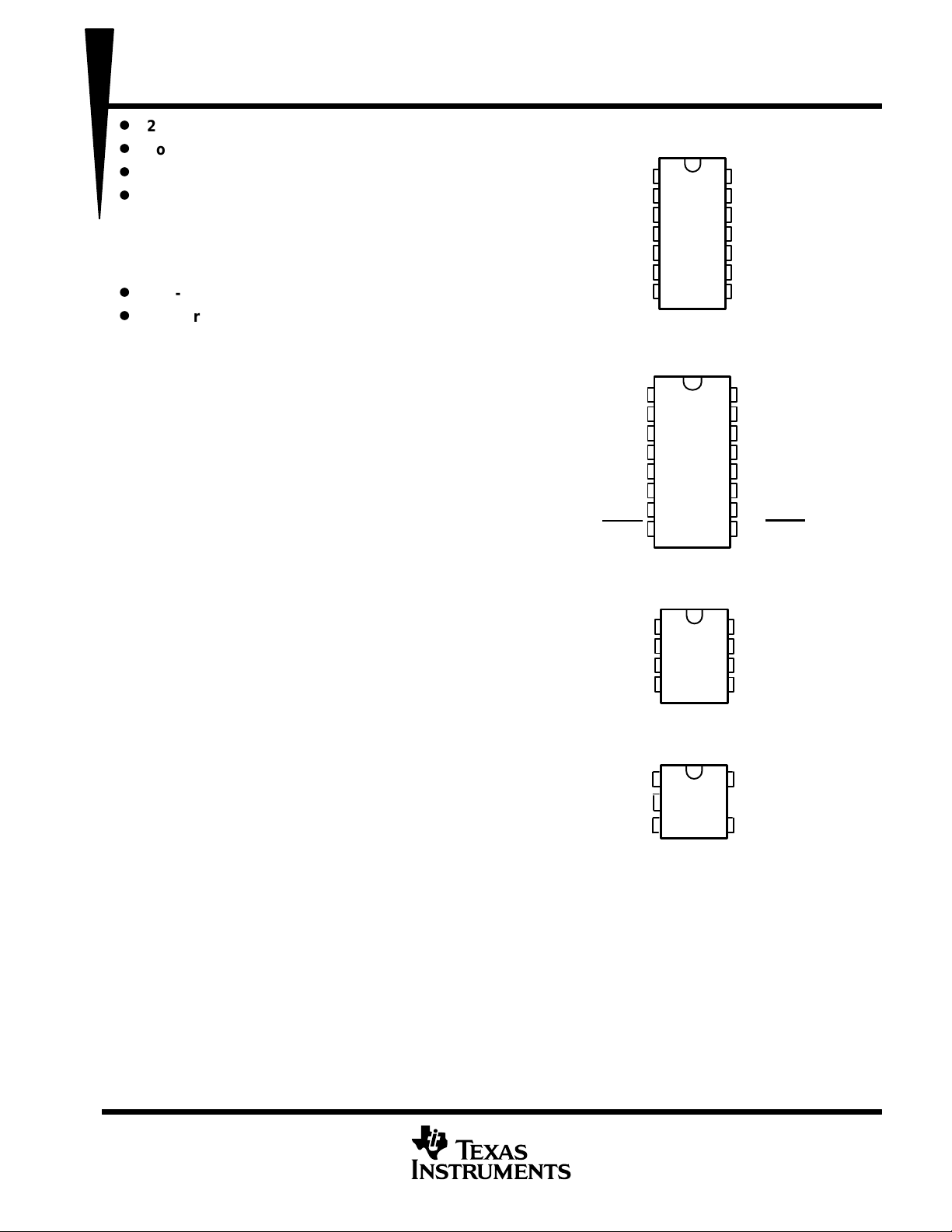
The LMV321 is available in the ultra-small DCK
(SC-70) package, which is approximately
one-half the size of the DBV (SOT-23) package.
This package saves space on printed circuit
boards and enables the design of small portable
electronic devices. It also allows the designer to
place the device closer to the signal source to
reduce noise pickup and increase signal integrity .
LMV324 ...D OR PW PACKAGE
1OUT
V
2OUT
LMV324S ...D OR PW PACKAGE
1OUT
1IN–
1IN+
2IN+
2IN–
2OUT
1/2 SHDN
LMV358 .. . D, DGK, OR PW PACKAGE
1OUT
LMV321 . . . DBV OR DCK PACKAGE
1IN–
1IN+
CC+
2IN+
2IN–
V
CC
1IN–
1IN+
GND
1IN+
GND
IN–
(TOP VIEW)
1
14
2
13
3
12
4
11
5
10
6
7
(TOP VIEW)
1
2
3
4
5
6
7
8
(TOP VIEW)
1
2
3
4
(TOP VIEW)
1
2
3
9
8
16
15
14
13
12
11
10
8
7
6
5
9
5
4
4OUT
4IN–
4IN+
GND
3IN+
3IN–
3OUT
V
OUT
4OUT
4IN–
4IN+
GND
3IN+
3IN–
3OUT
3/4 SHDN
V
CC+
2OUT
2IN–
2IN+
CC+
PRODUCTION DATA information is current as of publication date.
Products conform to specifications per the terms of Texas Instruments
standard warranty. Production processing does not necessarily include
testing of all parameters.
POST OFFICE BOX 655303 • DALLAS, TEXAS 75265
Copyright 2003, Texas Instruments Incorporated
1
LMV321 SINGLE, LMV358 DUAL, LMV324 QUAD, LMV324S QUAD WITH SHUTDOWN
SC-70 (DCK)
R3
Single
SOT23-5 (DBV)
RC1
SOIC (D)
MV358I
TSSOP (PW)
MV358I
LMV324I
SOIC (D)
Quad
LMV324SI
TSSOP (PW)
Reel of 2000
LOW-VOLTAGE RAIL-TO-RAIL OUTPUT OPERATIONAL AMPLIFIERS
SLOS263K – AUGUST 1999 – REVISED JUNE 2003
ORDERING INFORMATION
T
A
MSOP/VSSOP (DGK) Reel of 2500 LMV358IDGKR R5R
Dual
–40°C to 85°C
†
Package drawings, standard packing quantities, thermal data, symbolization, and PCB design guidelines are available at
www.ti.com/sc/package.
‡
DBV/DCK: The actual top-side marking has one additional character that designates the assembly/test site.
PACKAGE
†
Reel of 3000 LMV321IDCKR
Reel of 250 LMV321IDCKT
Reel of 3000 LMV321IDBVR
Reel of 250 LMV321IDBVT
Tube of 75 LMV358ID
Reel of 2500 LMV358IDR
Tube of 150 LMV358IPW
Reel of 2000 LMV358IPWR
Tube of 50 LMV324ID
Reel of 2500 LMV324IDR
Tube of 40 LMV324SID
Reel of 2500 LMV324SIDR
ORDERABLE
PART NUMBER
LMV324IPWR MV324I
LMV324SIPWR MV324SI
TOP-SIDE
MARKING
_
_
‡
symbol (each amplifier)
IN–
IN+
–
OUT
+
2
POST OFFICE BOX 655303 • DALLAS, TEXAS 75265
V
Amplifi
(LMV324S)
‡
V
VILAmplifier turn-off voltage level (LMV324S)
V
LMV321 SINGLE, LMV358 DUAL, LMV324 QUAD, LMV324S QUAD WITH SHUTDOWN
LOW-VOLTAGE RAIL-TO-RAIL OUTPUT OPERATIONAL AMPLIFIERS
SLOS263K – AUGUST 1999 – REVISED JUNE 2003
absolute maximum ratings over operating free-air temperature range (unless otherwise noted)
Supply voltage, V
Differential input voltage, V
Input voltage, V
Duration of output short circuit (one amplifier) to ground at (or below) T
V
≤ 5.5 V (see Note 3) Unlimited. . . . . . . . . . . . . . . . . . . . . . . . . . . . . . . . . . . . . . . . . . . . . . . . . . . . . . . . . . . . .
CC
Package thermal impedance,
(see Note 1) 5.5 V. . . . . . . . . . . . . . . . . . . . . . . . . . . . . . . . . . . . . . . . . . . . . . . . . . . . . . . . . . .
CC
(either input) 0 to 5.5 V. . . . . . . . . . . . . . . . . . . . . . . . . . . . . . . . . . . . . . . . . . . . . . . . . . . . . . . . . .
I
(see Note 2) ±5.5 V. . . . . . . . . . . . . . . . . . . . . . . . . . . . . . . . . . . . . . . . . . . . . . . . . .
ID
= 25°C,
A
θ
(see Notes 4 and 5): D (8-pin) package 97°C/W. . . . . . . . . . . . . . . . . . . . . .
JA
†
D (14-pin) package 86°C/W. . . . . . . . . . . . . . . . . . . .
D (16-pin) package 73°C/W. . . . . . . . . . . . . . . . . . . .
DBV package 206°C/W. . . . . . . . . . . . . . . . . . . . . . . .
DCK package 252°C/W. . . . . . . . . . . . . . . . . . . . . . . .
DGK package 172°C/W. . . . . . . . . . . . . . . . . . . . . . . .
PW (8-pin) package 149°C/W. . . . . . . . . . . . . . . . . . .
PW (14-pin) package 113°C/W. . . . . . . . . . . . . . . . . .
PW (16-pin) package 108°C/W. . . . . . . . . . . . . . . . . .
Operating virtual junction temperature, T
Storage temperature range, T
†
Stresses beyond those listed under “absolute maximum ratings” may cause permanent damage to the device. These are stress ratings only, and
functional operation of the device at these or any other conditions beyond those indicated under “recommended operating conditions” is not
implied. Exposure to absolute-maximum-rated conditions for extended periods may affect device reliability.
NOTES: 1. All voltage values (except differential voltages and VCC specified for the measurement of IOS) are with respect to the network GND.
2. Differential voltages are at IN+ with respect to IN–.
3. Short circuits from outputs to VCC can cause excessive heating and eventual destruction.
4. Maximum power dissipation is a function of TJ(max),
ambient temperature is PD = (TJ(max) – TA)/
5. The package thermal impedance is calculated in accordance with JESD 51-7.
–65 to 150°C. . . . . . . . . . . . . . . . . . . . . . . . . . . . . . . . . . . . . . . . . . . . . . . . . . . . .
stg
150°C. . . . . . . . . . . . . . . . . . . . . . . . . . . . . . . . . . . . . . . . . . . . . . . . . . .
J
θ
, and TA. The maximum allowable power dissipation at any allowable
θ
JA
JA
. Selecting the maximum of 150°C can affect reliability.
recommended operating conditions (see Note 6)
MIN MAX UNIT
V
T
‡
VIH should not be allowed to exceed VCC.
NOTE 6: All unused control inputs of the device must be held at VCC or GND to ensure proper device operation. Refer to the TI application report,
Supply voltage (single-supply operation) 2.7 5.5 V
CC
IH
A
er turn-on voltage level
p
Operating free-air temperature –40 85 °C
Implications of Slow or Floating CMOS Inputs, literature number SCBA004.
VCC = 2.7 V 1.7
VCC = 5 V 3.5
VCC = 2.7 V 0.7
VCC = 5 V 1.5
POST OFFICE BOX 655303 • DALLAS, TEXAS 75265
3
LMV321 SINGLE, LMV358 DUAL, LMV324 QUAD, LMV324S QUAD WITH SHUTDOWN
Output swing
R
10 kΩ to 1.35 V
mV
LOW-VOLTAGE RAIL-TO-RAIL OUTPUT OPERATIONAL AMPLIFIERS
SLOS263K – AUGUST 1999 – REVISED JUNE 2003
electrical characteristics at TA = 25°C and V
PARAMETER
V
a
I
IB
I
IO
CMRR Common-mode rejection ratio VCM = 0 to 1.7 V 50 63 dB
k
V
I
CC
B
F
G
V
I
n
Input offset voltage 1.7 7 mV
IO
Average temperature coefficient
V
IO
of input offset voltage
Input bias current 11 250 nA
Input offset current 5 50 nA
Supply-voltage rejection ratio VCC = 2.7 V to 5 V, VO = 1 V 50 60 dB
SVR
Common-mode input voltage range CMRR w 50 dB 0 to 1.7 –0.2 to 1.9 V
ICR
p
Supply current
Unity-gain bandwidth CL = 200 pF 1 MHz
1
Phase margin 60 deg
m
Gain margin 10 dB
m
Equivalent input noise voltage f = 1 kHz 46 nV/√Hz
n
Equivalent input noise current f = 1 kHz 0.17 pA/√Hz
=
L
LMV321I
LMV358I (both amplifiers)
LMV324I/LMV324SI (all four amplifiers) 260 680
shutdown characteristics (LMV324S) at TA = 25°C and V
PARAMETER
I
CC(SHDN)
t
(on)
t
(off)
Supply current in shutdown mode
(per channel)
Amplifier turn-on time AV = 1, RL = Open (measured at 50% point) 2
Amplifier turn-off time AV = 1, RL = Open (measured at 50% point) 40 ns
SHDN ≤ 0.6 V 5
= 2.7 V (unless otherwise noted)
CC+
TEST CONDITIONS MIN TYP MAX UNIT
5
High level VCC–100 VCC–10
Low level 60 180
80 170
140 340
= 2.7 V (unless otherwise noted)
CC+
TEST CONDITIONS MIN TYP MAX UNIT
m
V/°C
m
A
m
A
m
s
4
POST OFFICE BOX 655303 • DALLAS, TEXAS 75265
VIOInput offset voltage
mV
IIBInput bias current
nA
IIOInput offset current
nA
V
CMMR w 50 dB
25°C
0 to 4
2
V
High level
R
2 kΩ to 2.5 V
Low level
Output swing
mV
High level
R
10 kΩ to 2.5 V
Low level
A
gg
R
2 kΩ
V/mV
IOSOutput short-circuit current
25°C
mA
LMV321I
ICCSupply current
LMV358I (both
lifi
)
A
LMV321 SINGLE, LMV358 DUAL, LMV324 QUAD, LMV324S QUAD WITH SHUTDOWN
LOW-VOLTAGE RAIL-TO-RAIL OUTPUT OPERATIONAL AMPLIFIERS
SLOS263K – AUGUST 1999 – REVISED JUNE 2003
electrical characteristics at specified free-air temperature range, V
= 5 V (unless otherwise
CC+
noted)
PARAMETER TEST CONDITIONS T
p
a
CMRR Common-mode rejection ratio VCM = 0 to 4 V 25°C 50 65 dB
k
B
f
G
V
I
n
SR Slew rate 25°C 1 V/ms
Average temperature coefficient
V
IO
of input offset voltage
p
p
Supply-voltage rejection ratio
SVR
Common-mode
ICR
input voltage range
p
Large-signal differential
VD
voltage gain
p
pp
Unity-gain bandwidth CL = 200 pF 25°C 1 MHz
1
Phase margin 25°C 60 deg
m
Gain margin 25°C 10 dB
m
Equivalent input noise voltage f = 1 kHz 25°C 39 nV/√Hz
n
Equivalent input noise current f = 1 kHz 25°C 0.21 pA/√Hz
VCC= 2.7 V to 5 V, VO = 1 V,
VCM = 1 V
=
L
=
L
=
L
Sourcing, VO = 0 V
Sinking, VO = 5 V
amp
ers
LMV324I/LMV324SI
(all four amplifiers)
A
25°C 1.7 7
–40°C to 85°C 9
25°C 5
25°C 15 250
–40°C to 85°C 500
25°C 5 50
–40°C to 85°C 150
25°C 50 60 dB
25°C VCC–300 VCC–40
–40°C to 85°C VCC–400
25°C 120 300
–40°C to 85°C 400
25°C VCC–100 VCC–10
–40°C to 85°C VCC–200
25°C 65 180
–40°C to 85°C 280
25°C 15 100
–40°C to 85°C 10
25°C 130 250
–40°C to 85°C 350
25°C 210 440
–40°C to 85°C 615
25°C 410 830
–40°C to 85°C 1160
MIN TYP MAX UNIT
–0.2 to 4.
5 60
10 160
m
V/°C
m
shutdown characteristics (LMV324S) at TA = 25°C and V
I
CC(SHDN)
t
(on)
t
(off)
= 5 V (unless otherwise noted)
CC+
PARAMETER
Supply current in shutdown mode
(per channel)
Amplifier turn-on time AV = 1, RL = Open (measured at 50% point) 2
Amplifier turn-off time AV = 1, RL = Open (measured at 50% point) 40 ns
POST OFFICE BOX 655303 • DALLAS, TEXAS 75265
TEST CONDITIONS T
SHDN ≤ 0.6 V –40°C to 85°C 5
A
MIN TYP MAX UNIT
m
A
m
s
5
LMV321 SINGLE, LMV358 DUAL, LMV324 QUAD, LMV324S QUAD WITH SHUTDOWN
LOW-VOLTAGE RAIL-TO-RAIL OUTPUT OPERATIONAL AMPLIFIERS
SLOS263K – AUGUST 1999 – REVISED JUNE 2003
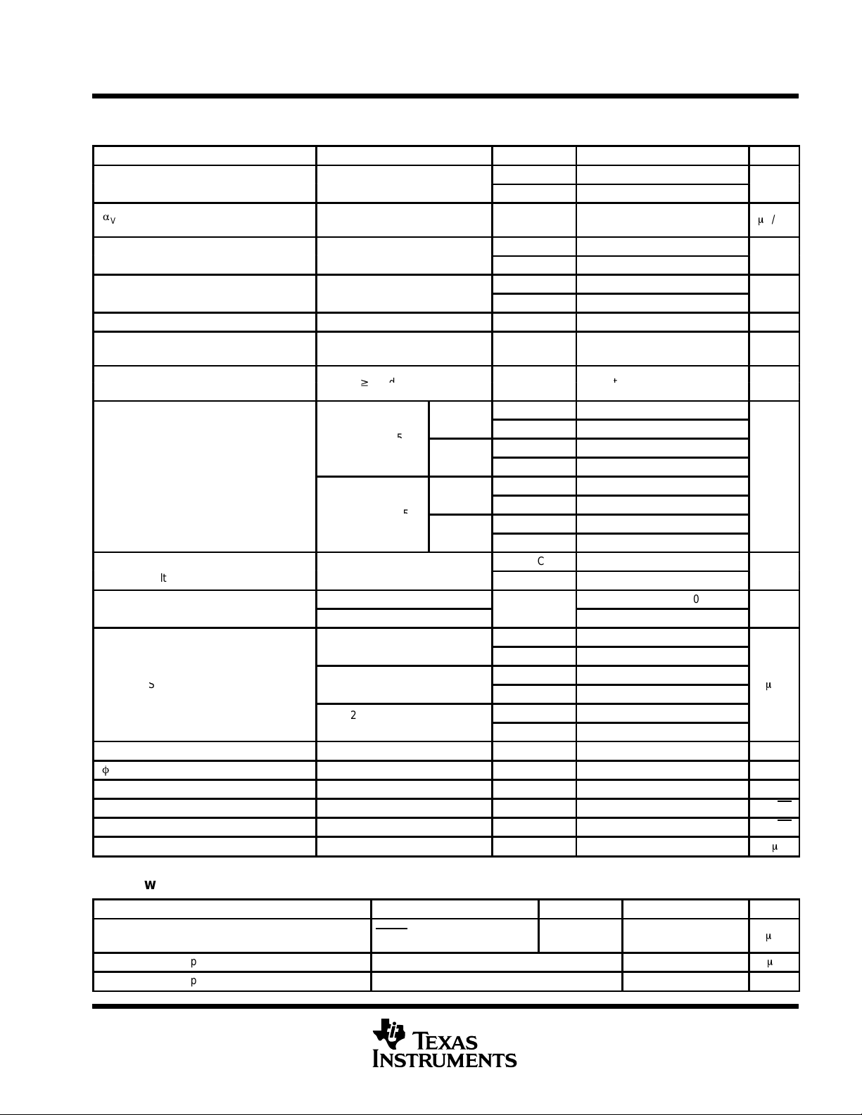
TYPICAL CHARACTERISTICS
Gain – dB
–10
–20
40
30
20
10
70
GAIN AND PHASE MARGIN
vs
FREQUENCY
Phase Margin – Deg
40
30
20
10
Gain – dB
–10
–20
0
1
VCC = 2.7 V
RL = 100 kΩ, 2 kΩ, 600 Ω
100 kΩ
2 kΩ
600 Ω
Phase
0
1
10 100
Frequency – kHz
Gain
1000
200
150
100
50
0
–50
10000
Figure 1
GAIN AND PHASE MARGIN
vs
FREQUENCY
100
70
GAIN AND PHASE MARGIN
vs
FREQUENCY
VCC = 5 V
RL = 100 kΩ, 2 kΩ, 600 Ω
100 kΩ
2 kΩ
600 Ω
Phase
10
Frequency – kHz
100 1000
Figure 2
GAIN AND PHASE MARGIN
vs
FREQUENCY
Gain
200
150
100
50
Phase Margin – Deg
0
–50
10000
100
60
50
40
30
20
Gain – dB
10
VCC = 5 V
0
RL = 600
CL = 16 pF, 100 pF,
–10
500 pF, 1000 pF
–20
10 100 1000 10000
Gain
W
Frequency – kHz
Phase
16 pF
100 pF
500 pF
1000 pF
16 pF
100 pF
500 pF
1000 pF
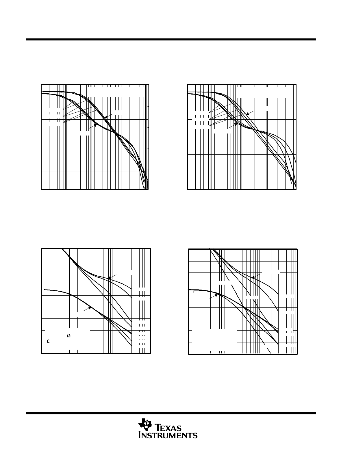
Figure 3
80
60
40
20
0
–20
–40
–60
–80
Phase Margin – Deg
60
50
40
30
Gain – dB
20
10
VCC = 5 V
0
RL = 100 kΩ
CL = 16 pF, 100 pF,
–10
500 pF, 1000 pF
–20
10
Gain
1000 pF
100
Frequency – kHz
Figure 4
500 pF
1000
Phase
1000 pF
16 pF
100 pF
16 pF
100 pF
500 pF
10000
80
60
40
20
0
–20
–40
–60
–80
Phase Margin – Deg
6
POST OFFICE BOX 655303 • DALLAS, TEXAS 75265
LMV321 SINGLE, LMV358 DUAL, LMV324 QUAD, LMV324S QUAD WITH SHUTDOWN
LOW-VOLTAGE RAIL-TO-RAIL OUTPUT OPERATIONAL AMPLIFIERS
SLOS263K – AUGUST 1999 – REVISED JUNE 2003
TYPICAL CHARACTERISTICS
GAIN AND PHASE MARGIN
vs
FREQUENCY
50
85°C
40
30
20
Gain – dB
10
VCC = 5 V
0
RL = 2 kΩ
TA = 85°C, 25°C, –40°C
–10
10 100 1000 10000
Gain
Frequency – kHz
25°C
–40°C
Phase
Figure 5
STABILITY
vs
CAPACITIVE LOAD
10000
2.5 V
_
+
V
I
R
L
1000
2.5 V
STABILITY
vs
CAPACITIVE LOAD
160
130
100
70
40
10
–20
Phase Margin – Deg
10000
1000
100
Capacitive Load – pF
10
LMV324S
(25% Overshoot)
LMV3xx
(25% Overshoot)
VCC = ±2.5 V
AV = +1
RL = 2 kΩ
VO = 100 mV
PP
Output Voltage – V
2.5 V
_
+
V
I
–2.5 V
R
L
V
O
C
L
1.510.50–0.5–1–1.5–2
Figure 6
STABILITY
vs
CAPACITIVE LOAD
10000
V
C
O
L
1000
VCC = ±2.5 V
RL = 2 kΩ
AV = 10
VO = 100 mV
PP
(25% Overshoot)
LMV324S
Capacitive Load – pF
100
10
LMV324S
(25% Overshoot)
LMV3xx
(25% Overshoot)
Output Voltage – V
Figure 7
100
Capacitive Load – nF
VCC = ±2.5 V
AV = +1
RL = 1 MΩ
VO = 100 mV
POST OFFICE BOX 655303 • DALLAS, TEXAS 75265
PP
10
1.510.50–0.5–1–1.5–2.0
134 kΩ
1.21 MΩ
+2.5 V
_
+
V
I
–2.5 V
R
Output Voltage – V
Figure 8
(25% Overshoot)
L
V
O
C
L
LMV3xx
1.510.50–0.5–1–1.5–2.0
7
LMV321 SINGLE, LMV358 DUAL, LMV324 QUAD, LMV324S QUAD WITH SHUTDOWN
LOW-VOLTAGE RAIL-TO-RAIL OUTPUT OPERATIONAL AMPLIFIERS
SLOS263K – AUGUST 1999 – REVISED JUNE 2003
TYPICAL CHARACTERISTICS
10000
Capacitive Load – nF
1000
100
700
600
500
STABILITY
vs
CAPACITIVE LOAD
VCC = ±2.5 V
10
RL = 1 MΩ
AV = 10
VO = 100 mV
134 kΩ
V
I
1.21 MΩ
+2.5 V
–2.5 V
PP
_
+
R
Output Voltage – V
(25% Overshoot)
LMV324S
(25% Overshoot)
V
O
L
C
L
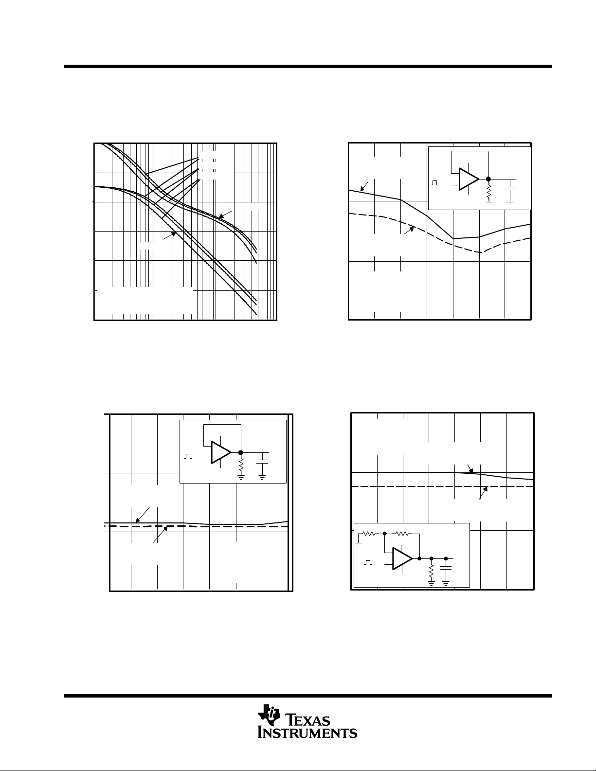
Figure 9
SUPPLY CURRENT
vs
SUPPLY VOLTAGE – QUAD AMPLIFIER
LMV3xx
LMV324S
LMV3xx
TA = 85°C
SLEW RATE
vs
SUPPLY VOLTAGE
1.500
1.400
1.300
1.200
µs
1.100
1.000
0.900
Slew Rate – V/
0.800
0.700
0.600
1.510.50–0.5–1–1.5–2.0
0.500
RL = 100 kΩ
NSLEW
LMV3xx
LMV324S
2.5 3.0 3.5 4.0 4.5 5.0
– Supply Voltage – V
V
CC
Gain
PSLEW
NSLEW
PSLEW
Figure 10
INPUT CURRENT
vs
TEMPERATURE
–10
VCC = 5 V
VI = VCC/2
–20
400
300
Supply Current – Aµ
200
100
0
012345
VCC – Supply Voltage – V
TA = 25°C
TA = –40°C
6
Figure 11
8
POST OFFICE BOX 655303 • DALLAS, TEXAS 75265
–30
LMV3xx
–40
Input Current – nA
–50
LMV324S
–60
–40 –30–20 –1001020304050607080
TA – °C
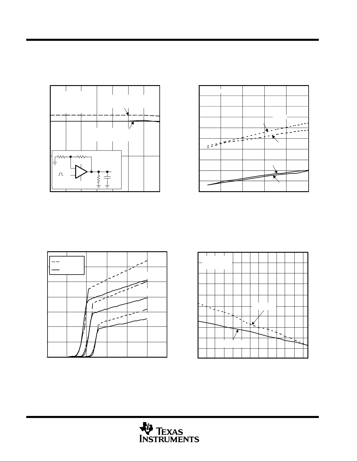
Figure 12

LMV321 SINGLE, LMV358 DUAL, LMV324 QUAD, LMV324S QUAD WITH SHUTDOWN
LOW-VOLTAGE RAIL-TO-RAIL OUTPUT OPERATIONAL AMPLIFIERS
SLOS263K – AUGUST 1999 – REVISED JUNE 2003
TYPICAL CHARACTERISTICS
SOURCE CURRENT
vs
OUTPUT VOLTAGE
100
VCC = 2.7 V
10
LMV3xx
1
0.1
Sourcing Current – mA
0.01
0.001
0.001 0.01 0.1 1 10
Output Voltage Referenced to V
LMV324S
Figure 13
SINKING CURRENT
vs
OUTPUT VOLTAGE
100
VCC = 2.7 V
CC+
– V
SOURCE CURRENT
vs
OUTPUT VOLTAGE
100
VCC = 5 V
10
1
0.1
Sourcing Current – mA
0.01
0.001
0.001 0.01 0.1 1 10
LMV3xx
LMV324S
Output Voltage Referenced to V
CC+
Figure 14
SINKING CURRENT
vs
100
VCC = 5 V
OUTPUT VOLTAGE
– V
10
LMV324S
1
LMV3xx
0.1
Sinking Current – mA
0.01
0.001
0.001 0.01 0.1 1 10
Output Voltage Referenced to GND – V
Figure 15
10
LMV324S
1
0.1
Sinking Current – mA
0.01
0.001
0.001 0.01 0.1 1 10
Output Voltage Referenced to GND – V
LMV324
Figure 16
POST OFFICE BOX 655303 • DALLAS, TEXAS 75265
9

LMV321 SINGLE, LMV358 DUAL, LMV324 QUAD, LMV324S QUAD WITH SHUTDOWN
LOW-VOLTAGE RAIL-TO-RAIL OUTPUT OPERATIONAL AMPLIFIERS
SLOS263K – AUGUST 1999 – REVISED JUNE 2003
TYPICAL CHARACTERISTICS
SHORT-CIRCUIT CURRENT
vs
TEMPERATURE
300
270
240
210
180
150
120
Sinking Current – mA
90
60
30
0
–40–30–20–100 102030405060708090
LMV324S
VCC = 5 V
LMV324S
VCC = 2.7 V
LMV3xx
VCC = 5 V
LMV3xx
VCC = 2.7 V
TA – °C
Figure 17
–k
SVR
vs
FREQUENCY
– dB
SVR
–k
80
70
60
50
40
30
20
10
LMV324S
LMV3xx
VCC = –5 V
RL = 10 kΩ
SHORT-CIRCUIT CURRENT
vs
TEMPERATURE
120
100
80
60
40
Sourcing Current – mA
20
0
–40 –30 –20–100 102030405060708090
LMV3xx
VCC = 2.7 V
LMV3xx
VCC = 5 V
LMV324S
VCC = 2.7 V
TA – °C
LMV324S
VCC = 5 V
Figure 18
+k
SVR
vs
FREQUENCY
– dB
SVR
+k
90
80
70
60
50
40
30
20
10
LMV3xx
LMV324S
VCC = 5 V
RL = 10 kΩ
10
0
100
1,000 10,000
Frequency – Hz
Figure 19
0
100,000
POST OFFICE BOX 655303 • DALLAS, TEXAS 75265
1,000,000
100
1,000
10,000
Frequency – Hz
Figure 20
100,000
1,000,000

LMV321 SINGLE, LMV358 DUAL, LMV324 QUAD, LMV324S QUAD WITH SHUTDOWN
LOW-VOLTAGE RAIL-TO-RAIL OUTPUT OPERATIONAL AMPLIFIERS
SLOS263K – AUGUST 1999 – REVISED JUNE 2003
TYPICAL CHARACTERISTICS
–k
SVR
vs
FREQUENCY
80
70
60
50
– dB
40
SVR
–k
30
20
10
0
100 1,000 10,000 100,000 1,000,000
LMV324S
LMV3xx
Frequency – Hz
VCC = –2.7 V
RL = 10 kΩ
Figure 21
OUTPUT VOLTAGE SWING
vs
SUPPLY VOLTAGE
70
RL = 10 kΩ
60
LMV3xx
Negative Swing
50
40
30
20
10
Positive Swing
LMV324S
+k
SVR
vs
FREQUENCY
80
70
60
50
– dB
40
SVR
30
+k
20
10
0
100 1,000 10,000 100,000 1,000,000
LMV324S
LMV3xx
Frequency – Hz
VCC = 2.7 V
RL = 10 kΩ
Figure 22
OUTPUT VOLTAGE
vs
FREQUENCY
OPP
Peak Output Voltage – V
6
5
4
3
2
1
LMV3xx
VCC = 5 V
LMV3xx
VCC = 2.7 V
RL = 10 kΩ
THD > 5%
AV = 3
LMV324S
VCC = 5 V
LMV324S
VCC = 2.7 V
Output Voltage Swing vs Supply Voltage – mV
0
2.5 3.0 3.5 4.0 4.5 5.0
VCC – Supply Voltage – V
Figure 23
POST OFFICE BOX 655303 • DALLAS, TEXAS 75265
0
1 10 100 1000 10000
Frequency – kHz
Figure 24
11

LMV321 SINGLE, LMV358 DUAL, LMV324 QUAD, LMV324S QUAD WITH SHUTDOWN
LOW-VOLTAGE RAIL-TO-RAIL OUTPUT OPERATIONAL AMPLIFIERS
SLOS263K – AUGUST 1999 – REVISED JUNE 2003
TYPICAL CHARACTERISTICS
OPEN-LOOP OUTPUT IMPEDANCE
vs
FREQUENCY
110
100
90
80
Ω
70
60
Impedance –
50
40
30
20
1 1000 2000 3000 4000
LMV3xx
VCC = 5 V
LMV324S
VCC = 5 V
Frequency – kHz
LMV3xx
VCC = 2.7 V
LMV324S
VCC = 2.7 V
Figure 25
CROSSTALK REJECTION
vs
FREQUENCY
150
VCC = 5 V
RL = 5 kΩ
140
130
120
110
Crosstalk Rejection – dB
100
90
100 1,000 10,000 100,000
Frequency – Hz
AV =
VO = 3 V
Figure 26
1
PP
12
POST OFFICE BOX 655303 • DALLAS, TEXAS 75265

LMV321 SINGLE, LMV358 DUAL, LMV324 QUAD, LMV324S QUAD WITH SHUTDOWN
LOW-VOLTAGE RAIL-TO-RAIL OUTPUT OPERATIONAL AMPLIFIERS
SLOS263K – AUGUST 1999 – REVISED JUNE 2003
TYPICAL CHARACTERISTICS
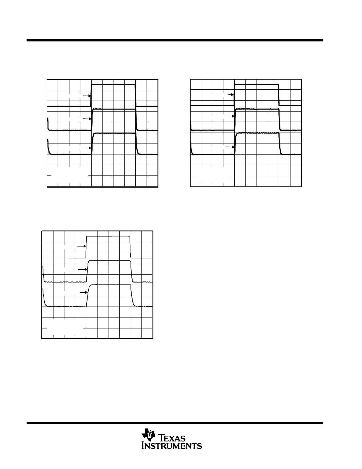
NONINVERTING LARGE-SIGNAL
PULSE RESPONSE
Input
LMV3xx
1 V/Div
LMV324S
VCC = ±2.5 V
RL = 2 kΩ
T = 25°C
1 µs/Div
Figure 27
NONINVERTING LARGE-SIGNAL
PULSE RESPONSE
1 V/Div
NONINVERTING LARGE-SIGNAL
PULSE RESPONSE
Input
LMV3xx
LMV324S
VCC = ±2.5 V
RL = 2 kΩ
TA = 85°C
1 µs/Div
Figure 28
1 V/Div
VCC = ±2.5 V
RL = 2 kΩ
TA = –40°C
Input
LMV3xx
LMV324S
1 µs/Div
Figure 29
POST OFFICE BOX 655303 • DALLAS, TEXAS 75265
13
LMV321 SINGLE, LMV358 DUAL, LMV324 QUAD, LMV324S QUAD WITH SHUTDOWN
LOW-VOLTAGE RAIL-TO-RAIL OUTPUT OPERATIONAL AMPLIFIERS
SLOS263K – AUGUST 1999 – REVISED JUNE 2003
TYPICAL CHARACTERISTICS
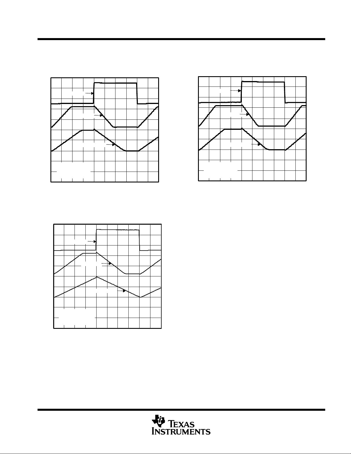
NONINVERTING SMALL-SIGNAL
PULSE RESPONSE
Input
LMV3xx
50 mV/Div
LMV324S
VCC = ±2.5 V
RL = 2 kΩ
TA = 25°C
1 µs/Div
Figure 30
NONINVERTING SMALL-SIGNAL
PULSE RESPONSE
50 mV/Div
VCC = ±2.5 V
RL = 2 kΩ
TA = 85°C
NONINVERTING SMALL-SIGNAL
PULSE RESPONSE
Input
LMV3xx
LMV324S
1 µs/Div
Figure 31
50 mV/Div
VCC = ±2.5 V
RL = 2 kΩ
TA = –40°C
Input
LMV3xx
LMV324S
1 µs/Div
Figure 32
14
POST OFFICE BOX 655303 • DALLAS, TEXAS 75265
LMV321 SINGLE, LMV358 DUAL, LMV324 QUAD, LMV324S QUAD WITH SHUTDOWN
LOW-VOLTAGE RAIL-TO-RAIL OUTPUT OPERATIONAL AMPLIFIERS
SLOS263K – AUGUST 1999 – REVISED JUNE 2003
TYPICAL CHARACTERISTICS
1 V/Div
INVERTING LARGE-SIGNAL
PULSE RESPONSE
Input
LMV3xx
LMV324S
VCC = ±2.5 V
RL = 2 kΩ
TA = 25°C
1 µs/Div
Figure 33
INVERTING LARGE-SIGNAL
PULSE RESPONSE
INVERTING LARGE-SIGNAL
PULSE RESPONSE
Input
LMV3xx
1 V/Div
LMV324S
VCC = ±2.5 V
RL = 2 kΩ
TA = 85°C
1 µs/Div
Figure 34
1 V/Div
Input
LMV3xx
LMV324S
VCC = ±2.5 V
RL = 2 kΩ
TA = –40°C
1 µs/Div
Figure 35
POST OFFICE BOX 655303 • DALLAS, TEXAS 75265
15

LMV321 SINGLE, LMV358 DUAL, LMV324 QUAD, LMV324S QUAD WITH SHUTDOWN
LOW-VOLTAGE RAIL-TO-RAIL OUTPUT OPERATIONAL AMPLIFIERS
SLOS263K – AUGUST 1999 – REVISED JUNE 2003
TYPICAL CHARACTERISTICS
50 mV/Div
VCC = ±2.5 V
RL = 2 kΩ
TA = 25°C
INVERTING SMALL-SIGNAL
PULSE RESPONSE
Input
LMV3xx
LMV324S
1 µs/Div
Figure 36
INVERTING SMALL-SIGNAL
PULSE RESPONSE
50 mV/Div
VCC = ±2.5 V
RL = 2 kΩ
TA = 85°C
INVERTING SMALL-SIGNAL
PULSE RESPONSE
Input
LMV3xx
LMV324S
1 µs/Div
Figure 37
50 mV/Div
VCC = ±2.5 V
RL = 2 kΩ
TA = –40°C
Input
LMV3xx
LMV324S
1 µs/Div
Figure 38
16
POST OFFICE BOX 655303 • DALLAS, TEXAS 75265

LMV321 SINGLE, LMV358 DUAL, LMV324 QUAD, LMV324S QUAD WITH SHUTDOWN
LOW-VOLTAGE RAIL-TO-RAIL OUTPUT OPERATIONAL AMPLIFIERS
SLOS263K – AUGUST 1999 – REVISED JUNE 2003
TYPICAL CHARACTERISTICS
Hz
Input Current Noise – pA/
0.80
0.60
0.40
0.20
0.00
200
INPUT CURRENT NOISE
vs
FREQUENCY
VCC = 2.7 V
10 Hz 100 Hz 1 KHz 10 KHz
Frequency
Figure 39
INPUT VOLTAGE NOISE
vs
FREQUENCY
Hz
Input Current Noise – pA/
0.50
0.45
0.40
0.35
0.30
0.25
0.20
0.15
0.10
0.05
0.00
INPUT CURRENT NOISE
vs
FREQUENCY
10 Hz 100 Hz 1 kHz
Frequency
Figure 40
VCC = 5 V
10 kHz
Input Voltage Noise – nV/ Hz
180
160
140
120
100
80
60
40
20
VCC = 5 V
10 Hz 100 Hz 1 kHz 10 kHz
Frequency
Figure 41
VCC = 2.7 V
POST OFFICE BOX 655303 • DALLAS, TEXAS 75265
17

LMV321 SINGLE, LMV358 DUAL, LMV324 QUAD, LMV324S QUAD WITH SHUTDOWN
LOW-VOLTAGE RAIL-TO-RAIL OUTPUT OPERATIONAL AMPLIFIERS
SLOS263K – AUGUST 1999 – REVISED JUNE 2003
TYPICAL CHARACTERISTICS
10.000
1.000
0.100
THD – %
0.010
0.001
10.000
1.000
VCC = 2.7 V
RL = 10 kΩ
AV = 1
VO = 1 V
10
VCC = 5 V
RL = 10 kΩ
AV = 1
VO = 1 V
PP
100
PP
THD + N
vs
FREQUENCY
1000
Frequency – Hz
Figure 42
THD + N
vs
FREQUENCY
LMV3xx
LMV324S
10000 100000
10.000
1.000
0.100
THD – %
0.010
0.001
10.000
1.000
VCC = 2.7 V
RL = 10 kΩ
AV = 10
VO = 1 V
10 100
PP
VCC = 5 V
RL = 10 kΩ
AV = 10
VO = 2.5 V
THD + N
vs
FREQUENCY
1000 10000
Frequency – Hz
Figure 43
THD + N
vs
FREQUENCY
PP
LMV324S
LMV3xx
100000
LMV324S
18
THD – %
0.100
0.010
0.001
10
100
1000
Frequency – Hz
Figure 44
LMV324S
LMV3xx
10000
POST OFFICE BOX 655303 • DALLAS, TEXAS 75265
100000
0.100
THD – %
0.010
0.001
10 100
LMV3xx
1000 10000 100000
Frequency – Hz
Figure 45

MECHANICAL DATA
MPDS018E – FEBRUARY 1996 – REVISED FEBRUARY 2002
DBV (R-PDSO-G5) PLASTIC SMALL-OUTLINE
0,95
1,45
0,95
3,00
2,80
45
31
0,05 MIN
5X
0,50
0,30
1,70
1,50
0,20
3,00
2,60
Seating Plane
M
0,15 NOM
Gage Plane
0,25
0°–8°
0,10
0,55
0,35
NOTES: A. All linear dimensions are in millimeters.
B. This drawing is subject to change without notice.
C. Body dimensions do not include mold flash or protrusion.
D. Falls within JEDEC MO-178
4073253-4/G 01/02
POST OFFICE BOX 655303 • DALLAS, TEXAS 75265
1

MECHANICAL DATA
MPDS025C – FEBRUARY 1997 – REVISED FEBRUARY 2002
DCK (R-PDSO-G5) PLASTIC SMALL-OUTLINE P ACKAGE
0,65
1,10
0,80
1 3
2,15
1,85
45
0,10
0,00
0,30
0,15
1,40
1,10
0,10
2,40
1,80
Seating Plane
M
0,13 NOM
Gage Plane
0,15
0°–8°
0,10
0,46
0,26
NOTES: A. All linear dimensions are in millimeters.
B. This drawing is subject to change without notice.
C. Body dimensions do not include mold flash or protrusion.
D. Falls within JEDEC MO-203
4093553-2/D 01/02
POST OFFICE BOX 655303 • DALLAS, TEXAS 75265
1

MECHANICAL DATA
MPDS028B – JUNE 1997 – REVISED SEPTEMBER 2001
DGK (R-PDSO-G8) PLASTIC SMALL-OUTLINE PACKAGE
0,65
8
1
1,07 MAX
3,05
2,95
0,38
0,25
5
3,05
2,95
4
Seating Plane
0,15
0,05
0,08
4,98
4,78
M
0,10
0,15 NOM
Gage Plane
0°–6°
0,25
0,69
0,41
NOTES: A. All linear dimensions are in millimeters.
B. This drawing is subject to change without notice.
C. Body dimensions do not include mold flash or protrusion.
D. Falls within JEDEC MO-187
4073329/C 08/01
POST OFFICE BOX 655303 • DALLAS, TEXAS 75265
1

MECHANICAL DATA
MSOI002B – JANUARY 1995 – REVISED SEPTEMBER 2001
D (R-PDSO-G**) PLASTIC SMALL-OUTLINE PACKAGE
8 PINS SHOWN
8 5
1 4
A
0.069 (1,75) MAX
0.020 (0,51)
0.014 (0,35)
0.157 (4,00)
0.150 (3,81)
0.010 (0,25)
0.004 (0,10)
0.244 (6,20)
0.228 (5,80)
0.010 (0,25)0.050 (1,27)
0.008 (0,20) NOM
Gage Plane
0.010 (0,25)
0°– 8°
0.044 (1,12)
0.016 (0,40)
Seating Plane
0.004 (0,10)
PINS **
DIM
A MAX
A MIN
NOTES: A. All linear dimensions are in inches (millimeters).
B. This drawing is subject to change without notice.
C. Body dimensions do not include mold flash or protrusion, not to exceed 0.006 (0,15).
D. Falls within JEDEC MS-012
8
0.197
(5,00)
0.189
(4,80)
14
0.344
(8,75)
0.337
(8,55)
16
0.394
(10,00)
0.386
(9,80)
4040047/E 09/01
POST OFFICE BOX 655303 • DALLAS, TEXAS 75265
1

MECHANICAL DATA
MTSS001C – JANUARY 1995 – REVISED FEBRUARY 1999
PW (R-PDSO-G**) PLASTIC SMALL-OUTLINE PACKAGE
14 PINS SHOWN
0,65
1,20 MAX
14
0,30
0,19
8
4,50
4,30
PINS **
7
Seating Plane
0,15
0,05
8
1
A
DIM
14
0,10
6,60
6,20
M
0,10
0,15 NOM
0°–8°
2016
Gage Plane
24
0,25
0,75
0,50
28
A MAX
A MIN
NOTES: A. All linear dimensions are in millimeters.
B. This drawing is subject to change without notice.
C. Body dimensions do not include mold flash or protrusion not to exceed 0,15.
D. Falls within JEDEC MO-153
3,10
2,90
5,10
4,90
5,10
4,90
6,60
6,40
7,90
7,70
9,80
9,60
4040064/F 01/97
POST OFFICE BOX 655303 • DALLAS, TEXAS 75265
1

IMPORTANT NOTICE
Texas Instruments Incorporated and its subsidiaries (TI) reserve the right to make corrections, modifications,
enhancements, improvements, and other changes to its products and services at any time and to discontinue
any product or service without notice. Customers should obtain the latest relevant information before placing
orders and should verify that such information is current and complete. All products are sold subject to TI’s terms
and conditions of sale supplied at the time of order acknowledgment.
TI warrants performance of its hardware products to the specifications applicable at the time of sale in
accordance with TI’s standard warranty . Testing and other quality control techniques are used to the extent TI
deems necessary to support this warranty . Except where mandated by government requirements, testing of all
parameters of each product is not necessarily performed.
TI assumes no liability for applications assistance or customer product design. Customers are responsible for
their products and applications using TI components. T o minimize the risks associated with customer products
and applications, customers should provide adequate design and operating safeguards.
TI does not warrant or represent that any license, either express or implied, is granted under any TI patent right,
copyright, mask work right, or other TI intellectual property right relating to any combination, machine, or process
in which TI products or services are used. Information published by TI regarding third-party products or services
does not constitute a license from TI to use such products or services or a warranty or endorsement thereof.
Use of such information may require a license from a third party under the patents or other intellectual property
of the third party , or a license from TI under the patents or other intellectual property of TI.
Reproduction of information in TI data books or data sheets is permissible only if reproduction is without
alteration and is accompanied by all associated warranties, conditions, limitations, and notices. Reproduction
of this information with alteration is an unfair and deceptive business practice. TI is not responsible or liable for
such altered documentation.
Resale of TI products or services with statements different from or beyond the parameters stated by TI for that
product or service voids all express and any implied warranties for the associated TI product or service and
is an unfair and deceptive business practice. TI is not responsible or liable for any such statements.
Following are URLs where you can obtain information on other Texas Instruments products and application
solutions:
Products Applications
Amplifiers amplifier.ti.com Audio www.ti.com/audio
Data Converters dataconverter.ti.com Automotive www.ti.com/automotive
DSP dsp.ti.com Broadband www.ti.com/broadband
Interface interface.ti.com Digital Control www.ti.com/digitalcontrol
Logic logic.ti.com Military www.ti.com/military
Power Mgmt power.ti.com Optical Networking www.ti.com/opticalnetwork
Microcontrollers microcontroller.ti.com Security www.ti.com/security
Telephony www.ti.com/telephony
Video & Imaging www.ti.com/video
Wireless www.ti.com/wireless
Mailing Address: Texas Instruments
Post Office Box 655303 Dallas, Texas 75265
Copyright 2003, Texas Instruments Incorporated
 Loading...