

Page 1

LMK05318EVM
User's Guide
Literature Number: SNAU236A
June 2018–Revised December 2018
Page 2

Contents
Preface ........................................................................................................................................ 5
1 EVM Quick Start................................................................................................................... 7
1.1 Device Revision Identification .......................................................................................... 8
1.2 Default EVM Configuration.............................................................................................. 8
2 Device Under Test .............................................................................................................. 10
2.1 Device Start-Up Modes ................................................................................................ 10
3 EVM Configuration ............................................................................................................. 11
3.1 Power Supply ........................................................................................................... 13
3.2 Logic Inputs and Outputs.............................................................................................. 15
3.3 XO Input ................................................................................................................. 18
3.4 Reference Clock Inputs ............................................................................................... 20
3.5 Clock Outputs ........................................................................................................... 20
3.6 Status Outputs and LEDs.............................................................................................. 21
4 EVM Schematics ................................................................................................................ 22
5 EVM Layouts...................................................................................................................... 33
6 EVM Bill of Materials........................................................................................................... 45
Appendix A Software .................................................................................................................. 51
A.1 Software Installation (One-Time).................................................................................... 51
A.2 TICS Pro Usage for LMK05318 ..................................................................................... 51
Revision History.......................................................................................................................... 52
2
Table of Contents
Copyright © 2018, Texas Instruments Incorporated
SNAU236A–June 2018–Revised December 2018
Submit Documentation Feedback
Page 3

www.ti.com
1 LMK05318EVM With Default Jumper and DIP Switch Settings ....................................................... 6
2 Key Components - EVM Top Side ...................................................................................... 12
3 Key Components - EVM Bottom Side................................................................................... 13
4 Default Power Jumper Configuration .................................................................................... 14
5 XO Input Interface (1 of 2) - 48.0048-MHz Oscillator and SMA Ports .............................................. 19
6 XO Input Interface (2 of 2) - LMK61E2 Oscillator ..................................................................... 20
7 Clock Input Interface - PRIREF (Similar for SECREF)................................................................ 20
8 Clock Output Interface - OUT0 (Similar for OUT1-OUT7) ............................................................ 21
9 Schematic 1 - Power Supplies............................................................................................ 22
10 Schematic 2 - Power Distribution ........................................................................................ 23
11 Schematic 3 - DC-DC Regulator ......................................................................................... 24
12 Schematic 4 - LMK05318 and XO Input Interfaces.................................................................... 25
13 Schematic 5 - Clock Input Interfaces .................................................................................... 26
14 Schematic 6 - Clock Output Interfaces (OUT0 to OUT3) ............................................................. 27
15 Schematic 7 - Clock Outputs (OUT4 to OUT7) ........................................................................ 28
16 Schematic 8 - Logic I/O Interfaces....................................................................................... 29
17 Schematic 9 - USB MCU and I
18 Schematic 10 - LMK61E2 Oscillator..................................................................................... 31
19 Schematic 11 - DUT Test Socket ........................................................................................ 32
20 Top Composite View....................................................................................................... 33
21 Top Solder Mask ........................................................................................................... 34
22 Layer 1 (Top Side) - Clock I/Os, Logic, and Power Routing, Ground Fill........................................... 35
23 Layer 2 - Ground Plane ................................................................................................... 36
24 Layer 3 - Logic Routing, Ground Fill..................................................................................... 37
25 Layer 4 - Power Routing, Ground Fill.................................................................................... 38
26 Layer 5 - Power and Ground Planes .................................................................................... 39
27 Layer 6 - Logic Routing, Ground Fill..................................................................................... 40
28 Layer 7 - Ground Plane ................................................................................................... 41
29 Layer 8 (Bottom Side, View From Top) - Logic and Power Routing, Ground Fill.................................. 42
30 Bottom Solder Mask ....................................................................................................... 43
31 Bottom Composite View................................................................................................... 44
List of Figures
2
C/SPI Jumper Block.................................................................. 30
SNAU236A–June 2018–Revised December 2018
Submit Documentation Feedback
Copyright © 2018, Texas Instruments Incorporated
List of Figures
3
Page 4

www.ti.com
List of Tables
1 Default Jumper and DIP Switch Settings ................................................................................ 7
2 Device Revision IDs......................................................................................................... 8
3 Default Configuration - EEPROM Start-Up Modes ..................................................................... 9
4 Device Start-Up Modes.................................................................................................... 10
5 Key EVM Components .................................................................................................... 11
6 Suggested DUT Power Configurations.................................................................................. 14
7 Suggested XO Power Configurations.................................................................................... 15
8 Logic Pin Mapping Tables................................................................................................. 15
9 Logic Pin Descriptions - EEPROM + I
10 Logic Pin Descriptions - EEPROM + SPI Mode (HW_SW_CTRL = Float) ........................................ 17
11 Logic Pin Descriptions - ROM + I
12 Bill of Materials ............................................................................................................. 45
2
C Mode (HW_SW_CTRL = 0) .............................................. 16
2
C Mode (HW_SW_CTRL = 1).................................................... 18
4
List of Tables
Copyright © 2018, Texas Instruments Incorporated
SNAU236A–June 2018–Revised December 2018
Submit Documentation Feedback
Page 5

Overview
The LMK05318EVM is an evaluation module for the LMK05318 Network Clock Generator and
Synchronizer. The EVM can be used for device evaluation, compliance testing, and system prototyping.
The LMK05318 integrates two Analog PLLs (APLL) and one Digital PLL (DPLL) with programmable loop
bandwidth. The EVM includes SMA connectors for clock inputs, oscillator inputs, and clock outputs to
interface the device with 50-Ω test equipment. The onboard XO allows the LMK05318 to be evaluated in
free-running, locked, or holdover mode of operation. The EVM can be configured through the onboard
USB microcontroller (MCU) interface using a PC with TI's TICS Pro software graphical user interface
(GUI). TICS Pro can be used to program the LMK05318 registers and on-chip EEPROM, which enables a
custom clock configuration on power up.
Trademarks
All trademarks are the property of their respective owners.
Features
• LMK05318 DUT:
– DPLL with programmable loop bandwidth for input jitter and wander attenuation
– Two Analog PLLs (APLLs) for flexible low-jitter clock generation
– Two clock inputs supporting hitless switching and holdover
– Eight differential clock outputs, or combination of differential and up to eight LVCMOS clocks
– On-chip EEPROM for custom start-up clocks
• SMA ports for clock input, oscillator inputs, and clock outputs
• Onboard oscillator options: 48.0048-MHz XO and LMK61E2 (I2C-programmable)
• USB MCU interface for I2C/SPI and GPIO pin control using TICS Pro GUI
• Status LEDs for power supplies and device status indicators
Preface
SNAU236A–June 2018–Revised December 2018
Introduction
What is Included
• LMK05318EVM
• Mini-USB cable
What is Needed
• Windows PC with TICS Pro Software GUI
• Test Equipment
– DC power supply (5 V, 1 A)
– Real-time oscilloscope
– Source signal analyzer
– Precision frequency counter
– Signal generator / reference clock
SNAU236A–June 2018–Revised December 2018
Submit Documentation Feedback
Copyright © 2018, Texas Instruments Incorporated
Preface
5
Page 6

What is Needed
www.ti.com
Figure 1. LMK05318EVM With Default Jumper and DIP Switch Settings
6
Introduction
Copyright © 2018, Texas Instruments Incorporated
SNAU236A–June 2018–Revised December 2018
Submit Documentation Feedback
Page 7
1 EVM Quick Start
This quick start guide can be followed to evaluate the LMK05318 DUT with the default EVM and device
configurations summarized in Section 1.2 and Table 3.
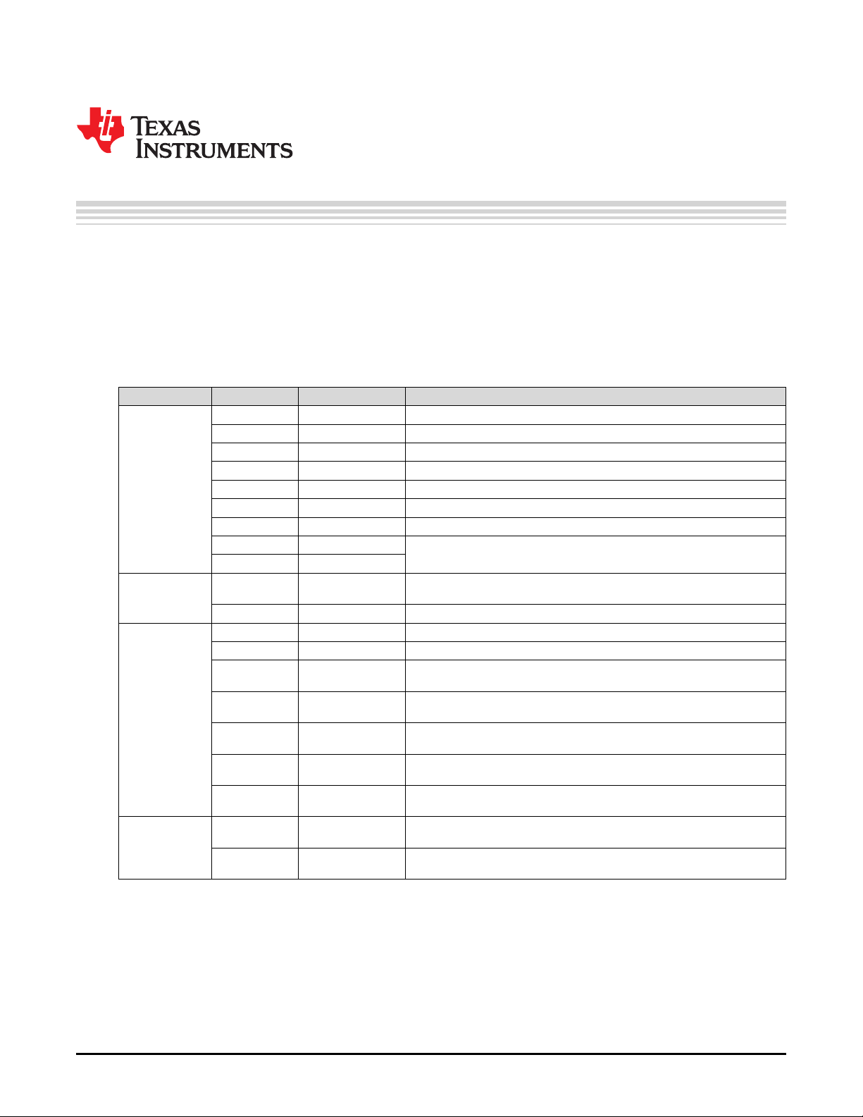
1. Verify the EVM default jumper and DIP switch settings shown in Figure 1 and Table 1:
CATEGORY REF DES POSITION DESCRIPTION
Power
Communication
DUT Control
Pins
DUT Loop Filter
Pins
User's Guide
SNAU236A–June 2018–Revised December 2018
LMK05318EVM User's Guide
Table 1. Default Jumper and DIP Switch Settings
JP1 Tie pins 1-2 DUT VDD = 3.3 V from LDO1
JP2 Tie pins 1-2 DUT VDDO = 1.8 V from LDO2
JP3 Tie pins 1-2 LDO3 IN powered from VIN1 external supply
JP4 Tie pins 1-2 1.8 V selected as LDO2 output voltage
JP16 Tie pins 1-2 VDDGPIO = 3.3 V
JP17 Tie pins 1-2 XO VCC = 3.3 V from LDO3
JP21 Tie pins 2-3 LMK61E2 VCC = GND (Powered off)
JP22 Tie pins 2-3
JP23 Tie pins 2-3
JP20
S9 S9[1:2] = OFF LMK61E2 I2C not connected to MCU
JP18 Tie pins 2-3 REFSEL = 0: PRIREF selected if using Manual Pin mode
JP19 Tie pins 2-3 HW_SW_CTRL = 0: EEPROM+I2C Start-up Mode selected
S2
S3
S5
S6
S7
S1
S10
Tie pins 1-2, 3-4,
11-12, and 13-14
S2[1:3] = OFF
S2[4] = ON
S3[1:3] = OFF
S3[4] = ON
S5[1] = ON
S5[2:3] = OFF
S6[1] = OFF
S6[2:3] = ON
S7[1] = OFF
S7[2:3] = ON
S1[1] = ON
S1[2:4] = OFF
S10[1] = ON
S10[2] = OFF
DC-DC Regulator VIN = GND (Powered off)
DUT I2C connected to MCU
STATUS0 = Hi-Z: Output state shown on D7. Pin not connected to MCU.
STATUS1/FDEC = Hi-Z: Output state shown on D8. Pin not connected to
MCU.
GPIO0/SYNCN = 1: SYNC deasserted. Pin not connected from MCU.
GPIO1/SCS = 0: I2C slave address = 0x64. Pin connected to MCU.
GPIO2/SDO/FINC = 0: Not used by default. Pin connected to MCU.
LF1 = 0.47 μF
LF2 = 0.1 μF
2. Connect +5 V from an external DC power supply (1-A limit) across the VIN1 and GND terminals of
header J1 (pins 1 and 4).
3. Toggle switch S4 (PDN/RESET) to reinitialize the DUT registers from on-chip EEPROM, if needed.
4. Check that the LEDs D7 and D8 are both ON if there is no valid clock input on PRIREF or SECREF.
This indicates that the DPLL is not locked and that the DPLL holdover is active.
a. When the DPLL is not locked, the clock outputs will free-run and track the frequency stability and
accuracy of the XO (Y1).
5. Connect an external 25-MHz single-ended clock input to either the PRIREF or SECREF SMA port to
SNAU236A–June 2018–Revised December 2018
Submit Documentation Feedback
Copyright © 2018, Texas Instruments Incorporated
LMK05318EVM User's Guide
7
Page 8

EVM Quick Start
lock the DPLL.
6. Check that the LEDs D7 and D8 are both OFF after a valid clock input is detected. This indicates the
that DPLL is locked and that the DPLL holdover is not active.
a. When the DPLL is locked, the output clocks should track the frequency accuracy of the clock input.
7. Check for any clock outputs on the OUT[0:7] SMA ports. TI recommends the following best practices
when making noise-sensitive performance measurements:
a. Use an appropriate balun to interface a differential output clock to the single-ended input of an RF
b. Properly terminate any active output clock trace by placing a 0-Ω load on the SMA port to minimize
NOTE: OUT7_P/N traces are DC-coupled to its SMA ports to allow evaluation of low-frequency
8. Connect the USB cable from connector J35 to the PC and configure the device through the TICS Pro
software to program the LMK05318 through the USB interface.
a. See Appendix A for TICS Pro installation and usage.
TICS Pro uses the "USB2ANY" API software driver to control the USB MCU interfaces (I2C/SPI and Logic
pins) on the EVM. TICS Pro can be used to access the device registers and program the device EEPROM
for a different start-up configuration.
www.ti.com
test equipment (phase noise or spectrum analyzer).
noise due to reflections. Otherwise, disable any unused outputs by register programming.
outputs (like 1 PPS) as well as LVCMOS or HCSL output types. Add an external DC blocking
cap between the OUT7 port and the input of any test equipment that cannot tolerate DC
bias.
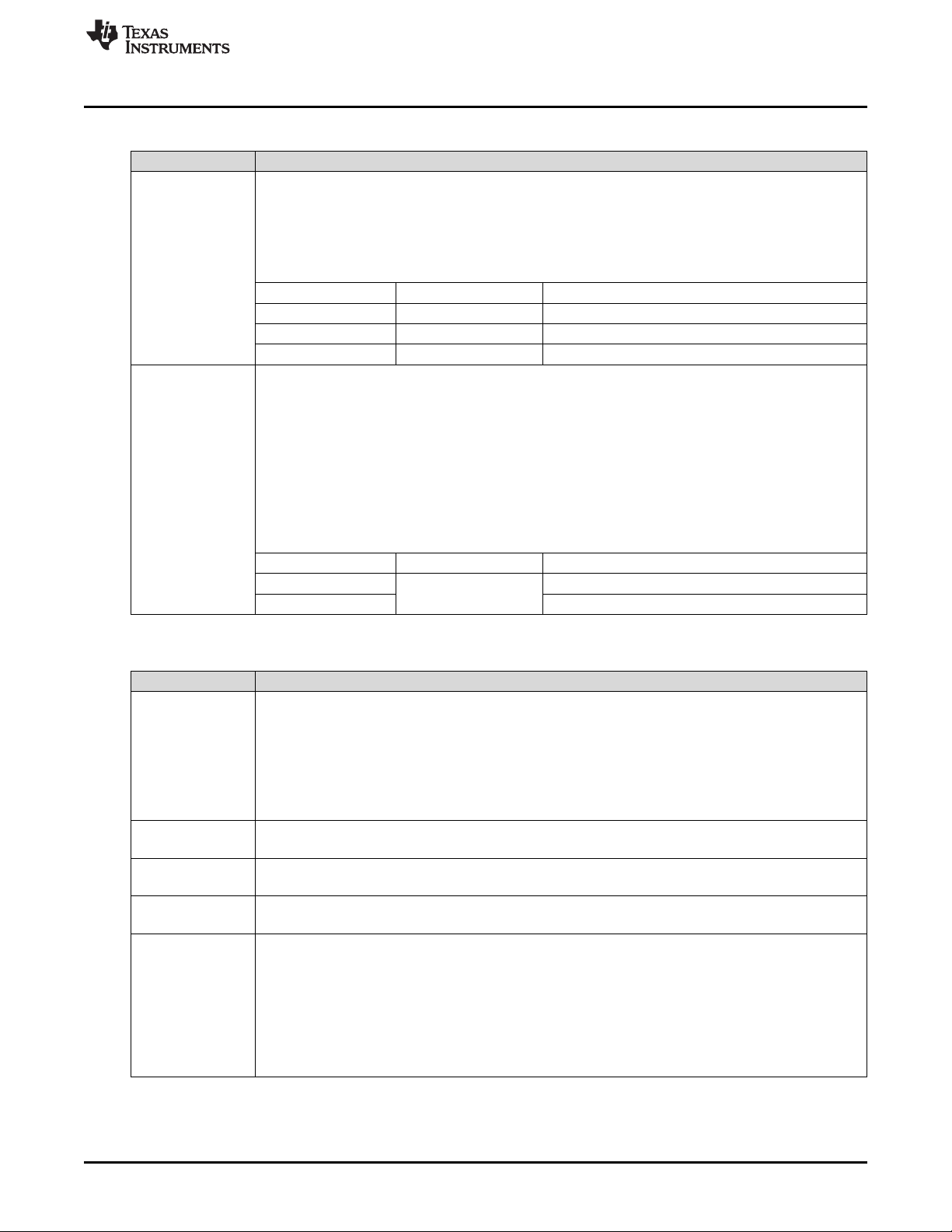
1.1 Device Revision Identification
Pre-production devices may have been distributed to customers as engineering sample parts or mounted
on pre-release EVMs. If a pre-production device or EVM is detected, TI recommends that the user replace
the pre-production device with a production device or EVM when available. Production samples and EVMs
can be ordered from product folder or requested through your local TI Field Sales representative.
The user can read the Device Revision ID (REVID) Register R3 to find the device revision in the TICS Pro
GUI or other serial host interface. See Table 2.
REVID REGISTER R3 VALUE DEVICE REVISION COMMENT
0x00 Pre-production device
0x11 Production device Okay to use.
1.2 Default EVM Configuration
• Power Supplies:
– VIN1: 5 V (External supply to onboard LDO regulators)
– DUT VDD: 3.3 V from LDO1 (U3)
– DUT VDDO: 1.8 V from LDO2 (U3)
– XO: 3.3 V from LDO3 (U4)
– VDDGPIO: 3.3 V from VDD
• LMK05318 DUT (U5):
– Clock Inputs:
• PRIREF and SECREF: DC-coupled from SMA ports
– Clock Outputs:
• OUT[0:6]: AC-coupled to SMA ports
• OUT7: DC-coupled to SMA ports
Table 2. Device Revision IDs
TI recommends to replace with a production device or EVM,
or contact TI Field Sales for technical support.
8
LMK05318EVM User's Guide
Copyright © 2018, Texas Instruments Incorporated
SNAU236A–June 2018–Revised December 2018
Submit Documentation Feedback
Page 9

www.ti.com
• Oscillators onboard:
EVM Quick Start
– XO (Y1), Default: 48.0048 MHz, 3.3 V, LVCMOS, low-jitter, ±25-ppm stability
– XO (U10), Alternate: LMK61E2, 10 to 1000 MHz (I2C-programmable), 3.3 V, Differential, low-jitter,
±50-ppm stability
NOTE: The EEPROM image of the LMK05318 was custom programmed to demonstrate the default
configuration in Table 3, which is different from the EEPROM image of generic factoryprogrammed devices.
Table 3. Default Configuration - EEPROM Start-Up Modes
DEVICE START-UP MODE
HW_SW_CTRL (JP19)
Jumper Setting
MCU I2C/SPI (JP20)
Jumper Settings
GPIO1/SCS (S6)
Jumper Settings
GPIO2/SDO/FINC (S7)
Jumper Settings
XO Input
PRIREF and SECREF Clock Inputs
DPLL Clock Input Assignment
DPLL Clock Input Selection Manual Fallback mode with Pin Select
PLL Mode DPLL Mode with APLL2 disabled
DPLL Loop Bandwidth 100 Hz
DPLL TDC Frequency 25 MHz
APLL1 VCO Frequency 2500 MHz
APLL2 VCO Frequency n/a (APLL2 disabled)
OUT[0:1] Output 156.25 MHz AC-LVPECL (from APLL1)
OUT[2:3] Output 156.25 MHz AC-LVPECL (from APLL1)
OUT[4] Output 156.25 MHz AC-LVPECL (from APLL1)
OUT[5] Output 156.25 MHz AC-LVPECL (from APLL1)
OUT[6] Output 156.25 MHz AC-LVPECL (from APLL1)
OUT[7] Output
PRIREF and SECREF
Frequency Detector Thresholds
PRIREF and SECREF
Window Detector Thresholds
DPLL Frequency Lock
Detector Thresholds
STATUS0 Output DPLL Loss of Lock (active high)
STATUS1 Output DPLL Holdover Active (active high)
(1)
Clock input frequency thresholds (ppm) are relative to the frequency accuracy of the XO input.
(1)
EEPROM + I2C MODE
(HW_SW_CTRL = 0)
Tie pins 2-3 Tie pins 2-4 (open)
Tie pins 1-2, 3-4, 11-12 and 13-14
MCU I2C interface to DUT
S6[1] = OFF, S6[2:3] = ON
GPIO1 = 0: I2C Address = 0x64h
S7[1] = OFF, S7[2:3] = ON
Not used by default
48.0048-MHz DIFF or LVCMOS
(On-chip termination disabled)
25-MHz DIFF or LVCMOS
(On-chip termination disabled)
PRIREF, SECREF
(Highest to lowest priority order)
156.25 MHz HCSL (from APLL1)
(On-chip termination disabled)
Not Enabled
33.6 ns (Early) < Valid REF Input Period < 46.4 ns (Late)
DPLL Locked < 1 ppm, DPLL Unlocked > 10 ppm
EEPROM + SPI MODE
(HW_SW_CTRL = Float)
Tie pins 7-8, 9-10, 11-12, and 13-14
MCU SPI interface to DUT
S6[1] = OFF, S6[2:3] = ON
SPI SCS input to MCU
S7[1] = OFF, S7[2:3] = ON
SPI SDO output to MCU
SNAU236A–June 2018–Revised December 2018
Submit Documentation Feedback
Copyright © 2018, Texas Instruments Incorporated
LMK05318EVM User's Guide
9
Page 10

Device Under Test
2 Device Under Test
The evaluation module is shipped with the LMK05318 DUT (U5) soldered down. The pin 1 position of the
48-pin QFN package is indicated by a dot symbol in top silkscreen. Alternatively, the U5 can be
unmounted and a test socket (XU1) can be populated. See for the socket part number. TI recommends
populating the socket with the hinge on the left-hand side (towards OUT[0:3] ports) and the latch on the
right-hand side.
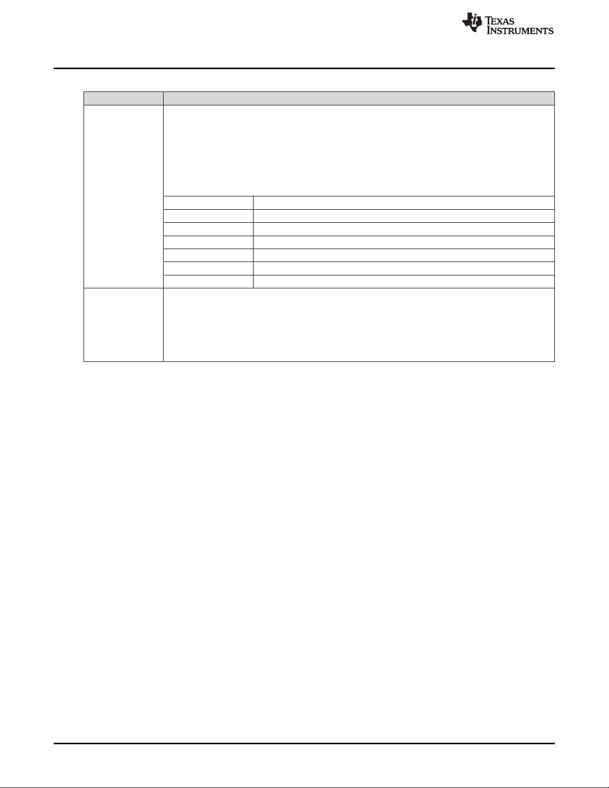
2.1 Device Start-Up Modes
The LMK05318 can start-up in one of three modes depending on the 3-level input level sampled on the
HW_SW_CTRL pin upon power-on reset (POR). The start-up modes are listed in Table 4 and determine
the following:
1. The memory bank (EEPROM or ROM) used to initialize the registers upon start-up.
2. The serial interface (I2C or SPI) used for register access.
3. The logic pin definitions.
The I2C or SPI interface allows for register access to configure the device after start-up and monitor its
status. The register map configurations are the same for I2C and SPI.
See Section 3.2 for detailed descriptions of the logic pins for each start-up mode.
HW_SW_CTRL
INPUT LEVEL
Float
(VIM)
(1)
The input levels on these pins are sampled only during POR.
(2)
FINC and FDEC pin controls are only available when DCO mode and GPIO pin control are enabled by registers.
(1)
START-UP MODE MODE DESCRIPTION
0
1
EEPROM + I2C
(Soft pin mode)
EEPROM + SPI
(Soft pin mode)
ROM + I2C
(Hard pin mode)
www.ti.com
Table 4. Device Start-Up Modes
Registers are initialized from EEPROM, and I2C interface is enabled with slave
address 11001xxb. Logic pins:
• SDA/SDI, SCL/SCK: I2C Data, I2C Clock
• GPIO0/SYNCN: Output Sync (active low)
• GPIO1/SCS
• GPIO2/SDO/FINC
• STATUS1/FDEC
output
Registers are initialized from EEPROM, and SPI interface is enabled. Logic pins:
• SDA/SDI, SCL/SCK: SPI Data In (SDI), SPI Clock (SCK)
• GPIO0/SYNCN: Output Sync (active low)
• GPIO1/SCS: SPI Chip Select (SCS)
• GPIO2/SDO/FINC: SPI Data Out (SDO)
Registers are initialized from the ROM page selected by GPIO pins, and I2C interface
is enabled with the 7-bit slave address of 0x64. Logic pins:
• SDA/SDI, SCL/SCK: I2C Data, I2C Clock
• GPIO[2:0]
• After POR, GPIO2/SDO/FINC and STATUS1/FDEC pins can function the same
as for HW_SW_CTRL = 0 if enabled by registers.
(1)
: I2C Address LSB Select (Low = 00b, Float = 01b, High = 10b)
(2)
: DPLL DCO Frequency Increment (active high)
(2)
: DPLL DCO Frequency Decrement (active high), or Status
(1)
: ROM page select at POR
10
TI suggests to use the EEPROM mode when either of the following is true:
• A single custom start-up frequency configuration is required from a single OPN.
• A host device is able to program the registers (and EEPROM, if needed) with a new configuration after
power-up through I2C or SPI. SPI is not supported by ROM mode.
LMK05318EVM User's Guide
Copyright © 2018, Texas Instruments Incorporated
SNAU236A–June 2018–Revised December 2018
Submit Documentation Feedback
Page 11

www.ti.com
NOTE: To ensure proper start-up into EEPROM + SPI Mode, the HW_SW_CTRL, STATUS0, and
STATUS1/FDEC pins must all be floating or biased to VIM(0.8-V typical) before the PDN pin
is pulled high. These three pins momentarily operate as 3-level inputs and get sampled at
the low-to-high transition of PDN to determine the device start-up mode during POR. If any of
these pins are connected to a host device (MCU or FPGA), TI recommends using external
biasing resistors on each pin (10-kΩ pullup to 3.3 V with 3.3-kΩ pulldown to GND) to set the
inputs to VIM during POR. After power-up, the STATUS pins can operate as LVCMOS
outputs and overdrive the external resistor bias for normal status operation.
3 EVM Configuration
The LMK05318 is a highly configurable clock chip with multiple power domains, PLL domains, and clock
input and output domains. To support a wide range of LMK05318 use cases, the EVM was designed with
more flexibility and functionality than needed to implement the chip in a customer system application.
This section describes the power, logic, and clock input and output interfaces on the EVM, as well as how
to connect, set up, and operate the EVM.
An overview of some key components are shown in Table 5, Figure 2, and Figure 3.
ITEM NO. REF DES DESCRIPTION
1 U5 LMK05318 DUT
2
3
A VIN1 (terminal) or
B J2 (SMA)
A Y1 or Y1: 48.0048-MHz XO (Default). Located on bottom side.
B J4/J5 or
C U10
4 J6/J7 and J8/J9 SMA Ports for DUT Clock Inputs (PRIREF_P/N and SECREF_P/N)
5
6 S4 Toggle Switch for DUT Power-Down/Reset (PDN pin)
7 JP18 Jumper for DUT Clock Input Selection (REFSEL)
8 D7, D8 Status LEDs for DUT STATUS[0:1] pins
9 JP20 Jumpers Header for I2C/SPI interface (MCU to DUT)
10 J35 USB Port for MCU
J12/J13, J14/J15,
J18/J19, J20/J21,
J24/25, J26/J27,
J30/J31, J32/J33
EVM Configuration
Table 5. Key EVM Components
External Supply Input (+5 V using default configuration)
J4/J5: SMA Ports for External XO_P/N input clock.
Requires minor rework before first use (see Section 3.3.1).
U10: LMK61E2 Programmable OSC.
Requires minor rework before first use (see Section 3.3.3).
SMA Ports for DUT Clock Outputs (OUT0_P/N to OUT7_P/N)
SNAU236A–June 2018–Revised December 2018
Submit Documentation Feedback
Copyright © 2018, Texas Instruments Incorporated
LMK05318EVM User's Guide
11
Page 12

OUT0_P
OUT0_N
OUT1_N
OUT1_P
OUT2_P
OUT2_N
OUT3_N
OUT3_P
OUT7_P
OUT7_N
OUT6_N
OUT6_P
OUT5_P
OUT5_N
OUT4_P
OUT4_N
PRIREF_P
PRIREF_N
SECREF_P
SECREF_N
2B
2A
3B
3C
1
4
5
5
6
7
8
9
10
VIN1
VIN2
1: LMK05318 DUT
2A: SMA Main Supply Input
2B: Terminal Main Supply Input
3B: SMA Ports for External XO
3C: Programmable XO
4: Reference Clock Inputs
5: Clock Outputs
6: PDN switch
7: Jumper for DPLL input sel.
8: Status LEDS
9: I2C/SPI Jumpers
10: USB port
EVM Configuration
www.ti.com
Figure 2. Key Components - EVM Top Side
12
LMK05318EVM User's Guide
SNAU236A–June 2018–Revised December 2018
Copyright © 2018, Texas Instruments Incorporated
Submit Documentation Feedback
Page 13

3A
OUT0_P
OUT0_N
OUT1_N
OUT1_P
OUT2_P
OUT2_N
OUT3_N
OUT3_P
OUT7_P
OUT7_N
OUT6_N
OUT6_P
OUT5_P
OUT5_N
OUT4_P
OUT4_N
PRIREF_P
PRIREF_N
SECREF_P
SECREF_N
VIN1
VIN2
4
2B
2B: Terminal Main Supply Input
3A: 48.0048-MHz XO
4: Reference Clock Inputs
www.ti.com
EVM Configuration
3.1 Power Supply
The LMK05318 has five core VDD supply pins that operate from 3.3 V ± 5% and six output VDDO supply
pins that operate from 1.8 V, 2.5 V, or 3.3 V ± 5%.
J1 is the main power terminal to the external power supply. Power SMA port VIN1 (J2) provides an
alternative connector style to apply power through coax cable.
Figure 3. Key Components - EVM Bottom Side
SNAU236A–June 2018–Revised December 2018
Submit Documentation Feedback
Copyright © 2018, Texas Instruments Incorporated
LMK05318EVM User's Guide
13
Page 14

5V
VDD: Select
3.3 V LDO1
LDO2 Output
Voltage (1.8 V)
VCCXO:
Select 3.3 V
from LDO3
VDDO:
Select LDO2
Out Voltage
EVM Configuration
On the EVM, the default power configuration uses the onboard LDO regulators to power all VDD and
VDDO pins from an external 5-V supply input VIN1 to J1 (or J2). A Dual LDO regulator (U3) is used to
power the VDD and VDDO rails of the DUT and its peripheral circuitry. A separate LDO regulator (U4),
also supplied from VIN1, is used to power the onboard XO circuits.
NOTE: Not every power connection is used or required to operate the EVM. Other power
Figure 4 shows the default power jumper locations and settings.
www.ti.com
configurations are possible. See the power schematics in Figure 9, Figure 10, and Figure 11.
Figure 4. Default Power Jumper Configuration
Table 6 shows the suggested power configurations for the DUT.
Table 6. Suggested DUT Power Configurations
CONNECTION NAME
(1)
J1
JP1 VDD
JP2 VDDO
JP4 VOUT2
(1)
The SMA ports J2 or J3 can be used to power VIN1 or VIN2, respectively, through a coaxial cable instead of using power cables
to J1.
PWR
ONBOARD LDO REGULATORS
VDDO = 1.8 / 2.5 / 3.3 V (LDO2)
Pin 1 (VIN1): Connect to external 5-V supply
Pin 2 (VIN2): n/a
Pin 3 (VIN3): n/a
Pin 4 (GND): Connect to supply ground
Tie pins 1-2: Selects 3.3 V from LDO1 to VDD
Plane
Tie pins 1-2: Selects LDO2 output to VDDO
Plane
Tie pins 1-2: LDO2 out = 1.8 V (default)
Tie pins 3-4: LDO2 out = 2.5 V
Tie pins 5-6: LDO2 out = 3.3 V
(DEFAULT)
VDD = 3.3 V (LDO1)
DIRECT EXTERNAL SUPPLIES
VDD = 3.3 V (EXT. VIN1)
VDDO = 1.8 / 2.5 / 3.3 V (EXT. VIN2)
Pin 1 (VIN1): Connect to external 3.3-V supply
Pin 2 (VIN2): Connect to external 1.8-V, 2.5-V,
or 3.3-V supply
Pin 3 (VIN3): n/a
Pin 4 (GND): Connect to supply ground
Tie pins 2-3:
Selects ext. 3.3V supply from VIN1 to VDD
Plane
Tie pins 2-3:
Selects ext. supply from VIN2 to VDDO Plane
n/a
14
LMK05318EVM User's Guide
Copyright © 2018, Texas Instruments Incorporated
SNAU236A–June 2018–Revised December 2018
Submit Documentation Feedback
Page 15

www.ti.com
Table 7 shows the suggested power configurations for the onboard XO circuits.
EVM Configuration
Table 7. Suggested XO Power Configurations
CONNECTION NAME
Pin 1 (VIN1): Connect to external 5-V supply
J1 PWR
JP3 LDO3 IN Tie pins 1-2: Selects 5 V from VIN1 to LDO3 IN n/a
JP17 VCCXO Tie pins 1-2: Select 3.3 V from LDO3
JP21 VCCLMK6 Tie pins 1-2: Selects 3.3 V from LDO3
Pin 2 (VIN2): n/a
Pin 3 (VIN3): n/a
Pin 4 (GND): Connect to supply ground
NOTE: Disconnect the power and signal paths from any XO circuit that is not used for a given
configuration to avoid unwanted noise coupling.
3.2 Logic Inputs and Outputs
The logic I/O pins of the DUT support different functions depending on the device start-up mode chosen
by the HW_SW_CTRL input level upon POR. The STATUS[0:1] pins are programmable and can be used
to monitor a variety of different device statuses.
The default logic input pin states are determined by onboard pullup or pulldown resistors, but some input
pins can be driven to high or low state by the MCU output or DIP switch control. The MCU can be
controlled from a PC running TICS Pro software to program the device registers through I2C or SPI and
also drive the DUT logic inputs.
See Table 8 for the logic pin mapping tables for the device start-up modes.
ONBOARD LDO REGULATOR
(DEFAULT)
LDO3 = 3.3 V (VIN3) VCCXO or VCCLMK6 = 3.3 V
n/a
Pin 1 (LDO3): Open
Pin 2 (VCCXO): Connect to external 3.3-V
supply
Pin 3 (GND): Connect to external supply ground
Pin 1 (LDO3): Open
Pin 2 (VCCLMK6): Connect to external 3.3-V
supply
Pin 3 (GND): Connect to external supply ground
DIRECT EXTERNAL SUPPLY
HW_SW_CTRL
(JP19)
0
(Tie pins 2-3)
Float
(Tie pins 2-4)
1
(Tie pins 1-2)
Logic pins not listed in Table 10 or Table 11 are the same as described in Table 9.
SNAU236A–June 2018–Revised December 2018
Submit Documentation Feedback
Table 8. Logic Pin Mapping Tables
START-UP MODE LOGIC PIN MAPPING TABLE
EEPROM + I2C
(Default)
EEPROM + SPI See Table 10
ROM + I2C See Table 11
Copyright © 2018, Texas Instruments Incorporated
See Table 9
LMK05318EVM User's Guide
15
Page 16

EVM Configuration
PIN NAME (TYPE) DESCRIPTION
PDN
(2-level input)
SDA/SDI
(Open-drain input)
SCL/SCK
(Open-drain input)
GPIO0/SYNCN
(2-level input)
GPIO1/SCS
(3-level input)
GPIO2/SDO/FINC
(2-level input)
Table 9. Logic Pin Descriptions - EEPROM + I2C Mode (HW_SW_CTRL = 0)
Chip Power-Down/Reset (active low)
When PDN rises to 1, the digital control block triggers the internal POR sequence, initializes all the registers
and logic pins for the start-up mode selected by the HW_SW_CTRL input level, restores all the internal
circuits including the serial interface to their initial state, and begins normal operation.
This pin is pulled high through an external pullup resistor, but can be pulled down by pushing toggle switch
S4.
PDN STATE S4 CHIP STATE
0 Pushed Power-down/reset state: Serial interface disabled
1 (Default) Released Normal operation
I2C Data (SDA)
The I2C interface between the DUT and MCU connects through two jumpers on JP20.
Tie JP20 pins 1-2 (SDA) and pins 3-4 (SCL) to connect the MCU and DUT to allow register programming
through I2C. Remove jumpers from JP20 pins 7-8 and pins 9-10 so the MCU SPI SCK and SDI pins are not
connected simultaneously.
Also, it is possible to use the EVM to program an off-board LMK05318 DUT by removing the I2C jumpers
from JP20, and connecting the MCU side (JP20 pins 1, 3, and 5) to the SDA, SCL, and GND lines of the
DUT on the target board. The MCU side of JP20 has external I2C pullup resistors to 3.3 V, which is derived
a dedicated regulator powered off the USB port 5-V supply.
I2C Clock (SCL)
See SDA/SDI pin description above. Red LED (D12) will turn ON during I2C activity.
Output Synchronization (active low)
GPIO0 (SYNCN) can be used to mute the output clocks and trigger output divider synchronization (SYNC) if
the divider SYNC bits are enabled by registers. Alternatively, SYNC can be triggered through register
programming instead of using this pin.
This pin is set through a 3-position DIP switch (S5). When S5[2] = ON (default), the pin is connected to the
MCU and can be driven 0 or 1 by software control. When S5[2] = OFF, the pullup or pulldown resistor switch
determines the GPIO0 state.
GPIO0 STATE S5 (0=OFF, 1=ON) OUTPUT SYNC STATE
0 S5[1:3] = 001
1 (Default) S5[1:3] = 100 SYNC deasserted: Normal output operation
I2C Slave Address LSB Select
GPIO1 is sampled on POR to configure the lower 2 bits of the 7-bit I2C address after start-up. The upper 5
bits of the I2C address are initialized from EEPROM (SLAVEADR[7:3] = 11001b).
This pin is set through a 3-position DIP switch (S6). When S6[2] = ON (default), the pin is connected to the
MCU and can be driven 0 or 1 by software control. When S6[2] = OFF, the pullup or pulldown resistor switch
determines the GPIO1 state.
GPIO1 STATE S6 (0=OFF, 1=ON) 7-BIT SLAVE ADDRESS
0 (Default) S6[1:3] = 001 1100100b (0x64h)
Float S6[1:3] = 000 1100101b (0x65h)
1 S6[1:3] = 100 1100111b (0x66h)
DPLL DCO Mode Frequency Increment (FINC)
When DCO mode and GPIO pin control are enabled by registers, a high pulse on the FINC input will
increment the DCO numerator by the programmable frequency deviation (FDEV) step size to adjust its
frequency.
This pin is set through a 3-position DIP switch (S7). When S7[2] = ON (default), the pin is connected to the
MCU and can be pulsed by software control. Alternatively, FINC can be triggered through register
programming without using this pin. When S7[2] = OFF, the pullup or pulldown switch determines the state.
FINC STATE S7 (0=OFF, 1=ON) DPLL DCO NUMERATOR
0
1 (Pulsed by MCU pin) Incremented
S7[1:3] = X1X
(MCU driven)
SYNC asserted: Outputs muted and output dividers held
in reset
No update
www.ti.com
16
LMK05318EVM User's Guide
SNAU236A–June 2018–Revised December 2018
Submit Documentation Feedback
Copyright © 2018, Texas Instruments Incorporated
Page 17
www.ti.com
Table 9. Logic Pin Descriptions - EEPROM + I2C Mode (HW_SW_CTRL = 0) (continued)
PIN NAME (TYPE) DESCRIPTION
DPLL Reference Clock Input Selection
The REFSEL pin selects the DPLL reference clock input when Manual Input Select mode and HW Pin
Control mode are selected by register configuration. This pin is ignored when Auto Input Select mode or SW
Register Control mode is selected.
This pin is set through a 3-way jumper (J18). When JP18 pins 2-4 are tied, the REFSEL pin is connected to
REFSEL
(2-level inputs)
STATUS0,
STATUS1/FDEC
(Logic outputs)
the MCU and can be driven 0 or 1 by software control. Otherwise, the REFSEL state is determined by the
other JP18 options below.
REFSEL STATE JP18 DPLL REF INPUT
0 (Default) Tie pins 2-3 PRIREF
Float Open pin 2 Auto Select
1 Tie pins 1-2 SECREF
Status Outputs
Each STATUS pin is a programmable status output that supports NMOS open-drain or 3.3-V LVCMOS
driver type. When S2[4] and S3[4] = ON, the output states of STATUS0 and STATUS1 are shown on activehigh LEDs D7 and D8, respectively. If STATUS0 or STATUS1 is configured as an open-drain driver, a 10-kΩ
pullup to VDDGPIO can be connected by setting S2[1] or S3[1] = ON.
DPLL DCO Mode Frequency Decrement (FDEC)
When DCO mode and GPIO pin control are enabled by registers, a high pulse on the FDEC input will
decrement the DCO numerator by the programmable frequency deviation (FDEV) step size to adjust its
frequency.
This pin is set through a 4-position DIP switch (S3). When S3[2] = ON, the pin is connected to the MCU and
can be pulsed by software control. Alternatively, FDEC can be triggered through register programming
without using this pin. When S3[2] = OFF, the pullup or pulldown switch determines the state.
FDEC STATE S3 (0=OFF, 1=ON) DPLL DCO NUMERATOR
0
1 (Pulsed by MCU pin) Decremented
S3[1:3] = X1X
(MCU driven)
No update
EVM Configuration
Table 10. Logic Pin Descriptions - EEPROM + SPI Mode (HW_SW_CTRL = Float)
(1) (2)
PIN NAME (TYPE) DESCRIPTION
SPI Data In (SDI / SIMO)
The SPI interface between the DUT and MCU can be connected using four jumpers on JP20.
SDA/SDI
(2-level input)
Tie JP20 pins 7-8 (SCL), pins 9-10 (SCL), pins 11-12 (SDO), and pins 13-14 (SCS) to connect the MCU and
DUT to allow register programming through SPI. Remove jumpers from JP20 pins 1-2 and pins 3-4, so the
MCU I2C pins are not connected simultaneously.
Also, it is possible to use the EVM to program an off-board LMK05318 DUT by removing the SPI jumpers
from JP20, and connecting the MCU side (JP20 pins 5, 7, 9, 11, and 13) to the GND, SCL, SDI, SDO, and
SCS lines of the DUT on the target board.
SCL/SCK
(2-level input)
GPIO1/SCS
(2-level input)
GPIO2/SDO/FINC
(2-level input)
SPI Clock (SCK)
See SDA/SDI pin description above. Red LED (D12) will turn ON during SPI activity.
SPI Chip Select (SCS)
See SDA/SDI pin description above.
SPI Data Out (SDO / SOMI)
See SDA/SDI pin description above.
Status Outputs
Both STATUS pins must be allowed to float during POR to ensure proper start-up into EEPROM+SPI Mode.
This means S2[1:3] and S3[1:3] must all be switched OFF during POR.
STATUS0,
STATUS1
(Logic outputs)
Each STATUS pin is a programmable status output that supports NMOS open-drain or 3.3-V LVCMOS
driver type. However, the 3.3-V LVCMOS driver type is recommended because external pullup resistors
must be avoided on the STATUS pins during POR when using EEPROM+SPI Mode. When S2[4] and S3[4]
= ON, the output states of STATUS0 and STATUS1 are shown on active-high LEDs D7 and D8,
respectively.
Note that DCO pin control is not supported in EEPROM+SPI mode.
(1)
Logic pins not listed in Table 10 are the same as described in Table 9.
(2)
When HW_SW_CTRL = Float, STATUS[1:0] pins must not be pulled high or low externally during POR to ensure proper start-up
into EEPROM+SPI Mode.
SNAU236A–June 2018–Revised December 2018
Submit Documentation Feedback
Copyright © 2018, Texas Instruments Incorporated
LMK05318EVM User's Guide
17
Page 18
EVM Configuration
PIN NAME (TYPE) DESCRIPTION
GPIO[2:0]
(2-level inputs)
STATUS0,
STATUS1/FDEC
(Logic outputs)
(1)
Logic pins not listed in Table 11 are the same as described in Table 9.
(2)
In ROM + I2C Mode, the two I2C address LSBs are forced to 00b (address = 0x64h).
Table 11. Logic Pin Descriptions - ROM + I2C Mode (HW_SW_CTRL = 1)
GPIO[2:0] Function at POR: ROM Page Selection
GPIO[2:0] pins are sampled on POR to select the ROM page settings used to initialize the registers.
The GPIO[2:0] pins are controlled by S7, S6, and S5, respectively. To configure GPIO[2:0] pins through the
pullup or pulldown resistors only (disable MCU control), set S5[2], S6[2], and S7[2] to OFF. Then, GPIOx
can be pulled up by setting Sy[1] = ON and Sy[3] = OFF, or else pulled down by setting Sy[1] = OFF and
Sy[3] = ON.
GPIO2 Function after POR: DPLL DCO Mode Frequency Increment (FINC)
After POR, the GPIO2 pin can be operated as an FINC input in the same way described for EEPROM + I2C
mode (see the GPIO2/FINC description in Table 9).
GPIO[2:0] STATES ROM PAGE SELECT
000b (Default) ROM Page 0
001b ROM Page 1
010b ROM Page 2
... ...
110b ROM Page 6
111b ROM Page 7
Status Outputs
STATUS[1:0] pins are individually programmable status outputs that support NMOS open-drain (requires
external pullup resistor) or 3.3-V LVCMOS driver type. The state of these pins is shown by D7 and D8 when
S2[4] and S3[4] are ON, respectively.
DPLL DCO Mode Frequency Decrement (FDEC)
After POR, the STATUS1 pin can be operated as an FDEC input in the same way described for EEPROM +
I2C mode (see the STATUS1/FDEC description in Table 9).
(1)(2)
www.ti.com
3.3 XO Input
The LMK05318 has an XO input (XO_P/N pins) to accept a reference clock for the Fractional-N APLLs.
The XO input determines the output frequency accuracy and stability in free-run or holdover modes. For
synchronization applications like SyncE or IEEE 1588, the XO input would typically be driven by a lowfrequency TCXO, OCXO, or external traceable clock that conforms to the frequency accuracy and
holdover stability requirements of the application. For DPLL mode, the XO frequency must have a non-
integer frequency relationship with the VCO1 frequency so APLL1 operates in Fractional mode. For APLL
only mode (DPLL not used), the XO frequency can have an integer relationship with the VCO1 and/or
VCO2 frequencies to avoid fractional spurs.
The XO input of the LMK05318 has programmable on-chip input termination and AC-coupled input biasing
options to support any clock interface type.
For flexibility, the EVM provides the three XO input options (use one at a time).
3.3.1 48.0048-MHz Oscillator (Default)
By default, the EVM is populated with a 48.0048-MHz, 3.3-V LVCMOS, low-jitter oscillator (Y1) to drive the
XO_P input of the DUT with the onboard termination and AC coupling. See Figure 5. Y1 can be used to
evaluate various frequency configurations. Y1 has multiple overlapped 4-pin SMD footprints (2.5×2.0,
3.2×2.5, 5×7, or 9×14-mm sizes) that allows the user to rework a different XO frequency/model after the
pre-installed component is carefully removed.
3.3.2 External Clock Input
Another option is to feed an external clock to the SMA ports (J5/J4) to drive the XO_P/N inputs
(differential) or XO_P input (single-ended). See Figure 5. This path can be connected to the XO_P/N input
pins by placing 0.1-µF capacitors on C81 and C82 and opening C80, C137, and C138. Y1 and U10 should
be powered down when using the external XO input path.
18
LMK05318EVM User's Guide
Copyright © 2018, Texas Instruments Incorporated
SNAU236A–June 2018–Revised December 2018
Submit Documentation Feedback
Page 19

www.ti.com
EVM Configuration
NOTE: Disconnect the power and signal paths from any XO circuit that is not used for a given
configuration to avoid unwanted spurious noise on the board. Y1 can be powered down by
JP17 (Tie pins 2-3). U10 can be powered down by JP21 (Tie pins 2-3).
Figure 5. XO Input Interface (1 of 2) - 48.0048-MHz Oscillator and SMA Ports
3.3.3 LMK61E2 Programmable Oscillator
The last option is to use the other onboard LMK61E2 programmable oscillator (U10) to drive the XO_P/N
inputs. See Figure 6.
The differential output clock from U10 can be routed to the XO_P/N input pins with minimal rework by
placing 0.1-µF capacitors on C137 and C138, and opening C80, C81, and C82 (note: C137 shares a pad
with C80 and C81, and C138 shares a pad with C82). U10 can be powered by a clean 3.3-V supply from
LDO3 by tying JP21 pins 1-2.
SNAU236A–June 2018–Revised December 2018
Submit Documentation Feedback
Copyright © 2018, Texas Instruments Incorporated
LMK05318EVM User's Guide
19
Page 20

1
234
5
J6
PRIREF_P
1
234
5
J7
PRIREF_N
SMA_PRI_P
SMA_PRI_N
0
C86
0
C87
0
R47
0
R46
0
R57
0
R56
49.9
R50
DNP
49.9
R52
DNP
C_PRI_P
C_PRI_N
R_PRI_P
R_PRI_N
100
R54
DNP
PRIREF_P
PRIREF_N
EVM Configuration
U10 can be configured to output any other supported XO frequency by programming it through the I2C
interface of the MCU. To connect U10 to the I2C bus (shared with the DUT), set switches S9[1:2] to the
ON positions. The user can select the LMK61E2 device profile in TICS Pro, scan the I2C bus to detect
U10 at address 0x58, configure the output to a different frequency, and store the new configuration to the
LMK61E2's internal EEPROM if desired. After U10 has been programmed, set S9[1:2] to the OFF
positions to disconnect it from the I2C bus.
www.ti.com
Figure 6. XO Input Interface (2 of 2) - LMK61E2 Oscillator
3.4 Reference Clock Inputs
The LMK05318 has two DPLL reference clock input pairs (PRIREF_P/N and SECREF_P/N) with
configurable input priority and input selection modes. The inputs have programmable input type,
termination, and biasing options to support any clock interface type.
External LVCMOS or Differential reference clock inputs can be applied to the SMA ports, labeled
PRIREF_P/N and SECREF_P/N. All SMA inputs are routed through 50-Ω single-ended traces and DCcoupled to the corresponding PRIREF_P/N and SECREF_P/N pins of the DUT.
3.5 Clock Outputs
The LMK05318 has eight clock output pairs (OUT[0:7]_P/N) that can be sourced from either APLL
20
domain.
LMK05318EVM User's Guide
Figure 7. Clock Input Interface - PRIREF (Similar for SECREF)
Copyright © 2018, Texas Instruments Incorporated
SNAU236A–June 2018–Revised December 2018
Submit Documentation Feedback
Page 21

49.9
R74
DNP
49.9
R75
DNP
1
234
5
J12
OUT0_P
1
234
5
J13
OUT0_N
49.9
R64
DNP
49.9
R65
DNP
O0_P
O0_N
100
R69
DNP
SMA_O0_P
SMA_O0_N
OUT0_P
OUT0_N
0
R60
0
R61
0
R68
DNP
0
R70
DNP
0.1uF
C90
0.1uF
C91
1 2
3 4
J10
DNP
www.ti.com
Output clocks are routed through 50-Ω single-ended traces and AC-coupled to the SMA ports labeled
OUT[0:6]_P/N. The OUT7_P/N is also routed through 50-Ω single-ended traces, but is DC-coupled to the
SMA ports to allow for evaluation of low frequency outputs (for example, 1 PPS or 1 Hz), as well as
LVCMOS or HCSL output clocks. Each output pair supports AC-LVDS/CML/LVPECL and HCSL driver
types. The HCSL driver has programmable on-chip termination or can used external termination. OUT[4:7]
can also support 1.8-V LVCMOS driver type with one or two LVCMOS output clocks per P/N pair. Each
LVCMOS driver has internal 50-Ω output impedance and supports programmable polarity and tri-state
options.
EVM Configuration
Figure 8. Clock Output Interface - OUT0 (Similar for OUT1-OUT7)
3.6 Status Outputs and LEDs
Status outputs signals can be configured on the STATUS0 and STATUS1/FDEC pins. The status output
signal, output type (3.3-V LVCMOS or NMOS open-drain), and output polarity are register programmable.
The output states for these pins (and other logic pins) can be probed at header J34 (not installed).
STATUS0 and STATUS1 outputs drive orange LEDs D7 and D8 for visual indication. Each LED will turn
ON when the status output is 1 (active high).
SNAU236A–June 2018–Revised December 2018
Submit Documentation Feedback
Copyright © 2018, Texas Instruments Incorporated
LMK05318EVM User's Guide
21
Page 22

EVM Schematics
4 EVM Schematics
www.ti.com
22
LMK05318EVM User's Guide
Figure 9. Schematic 1 - Power Supplies
SNAU236A–June 2018–Revised December 2018
Submit Documentation Feedback
Copyright © 2018, Texas Instruments Incorporated
Page 23

www.ti.com
EVM Schematics
SNAU236A–June 2018–Revised December 2018
Submit Documentation Feedback
Figure 10. Schematic 2 - Power Distribution
Copyright © 2018, Texas Instruments Incorporated
LMK05318EVM User's Guide
23
Page 24

EVM Schematics
www.ti.com
24
LMK05318EVM User's Guide
Figure 11. Schematic 3 - DC-DC Regulator
SNAU236A–June 2018–Revised December 2018
Submit Documentation Feedback
Copyright © 2018, Texas Instruments Incorporated
Page 25

www.ti.com
EVM Schematics
SNAU236A–June 2018–Revised December 2018
Submit Documentation Feedback
Figure 12. Schematic 4 - LMK05318 and XO Input Interfaces
Copyright © 2018, Texas Instruments Incorporated
LMK05318EVM User's Guide
25
Page 26

EVM Schematics
www.ti.com
26
LMK05318EVM User's Guide
Figure 13. Schematic 5 - Clock Input Interfaces
SNAU236A–June 2018–Revised December 2018
Submit Documentation Feedback
Copyright © 2018, Texas Instruments Incorporated
Page 27

www.ti.com
EVM Schematics
SNAU236A–June 2018–Revised December 2018
Submit Documentation Feedback
Figure 14. Schematic 6 - Clock Output Interfaces (OUT0 to OUT3)
Copyright © 2018, Texas Instruments Incorporated
LMK05318EVM User's Guide
27
Page 28

EVM Schematics
www.ti.com
28
LMK05318EVM User's Guide
Figure 15. Schematic 7 - Clock Outputs (OUT4 to OUT7)
SNAU236A–June 2018–Revised December 2018
Submit Documentation Feedback
Copyright © 2018, Texas Instruments Incorporated
Page 29

www.ti.com
EVM Schematics
SNAU236A–June 2018–Revised December 2018
Submit Documentation Feedback
Figure 16. Schematic 8 - Logic I/O Interfaces
Copyright © 2018, Texas Instruments Incorporated
LMK05318EVM User's Guide
29
Page 30

EVM Schematics
www.ti.com
30
LMK05318EVM User's Guide
Figure 17. Schematic 9 - USB MCU and I2C/SPI Jumper Block
SNAU236A–June 2018–Revised December 2018
Submit Documentation Feedback
Copyright © 2018, Texas Instruments Incorporated
Page 31

www.ti.com
EVM Schematics
SNAU236A–June 2018–Revised December 2018
Submit Documentation Feedback
Figure 18. Schematic 10 - LMK61E2 Oscillator
Copyright © 2018, Texas Instruments Incorporated
LMK05318EVM User's Guide
31
Page 32

EVM Schematics
www.ti.com
32
LMK05318EVM User's Guide
Figure 19. Schematic 11 - DUT Test Socket
SNAU236A–June 2018–Revised December 2018
Submit Documentation Feedback
Copyright © 2018, Texas Instruments Incorporated
Page 33

www.ti.com
5 EVM Layouts
EVM Layouts
SNAU236A–June 2018–Revised December 2018
Submit Documentation Feedback
Figure 20. Top Composite View
Copyright © 2018, Texas Instruments Incorporated
LMK05318EVM User's Guide
33
Page 34

EVM Layouts
www.ti.com
34
LMK05318EVM User's Guide
Figure 21. Top Solder Mask
Copyright © 2018, Texas Instruments Incorporated
SNAU236A–June 2018–Revised December 2018
Submit Documentation Feedback
Page 35

www.ti.com
EVM Layouts
Figure 22. Layer 1 (Top Side) - Clock I/Os, Logic, and Power Routing, Ground Fill
SNAU236A–June 2018–Revised December 2018
Submit Documentation Feedback
Copyright © 2018, Texas Instruments Incorporated
LMK05318EVM User's Guide
35
Page 36
EVM Layouts
www.ti.com
36
LMK05318EVM User's Guide
Figure 23. Layer 2 - Ground Plane
Copyright © 2018, Texas Instruments Incorporated
SNAU236A–June 2018–Revised December 2018
Submit Documentation Feedback
Page 37
www.ti.com
EVM Layouts
Figure 24. Layer 3 - Logic Routing, Ground Fill
SNAU236A–June 2018–Revised December 2018
Submit Documentation Feedback
Copyright © 2018, Texas Instruments Incorporated
LMK05318EVM User's Guide
37
Page 38

EVM Layouts
www.ti.com
38
LMK05318EVM User's Guide
Figure 25. Layer 4 - Power Routing, Ground Fill
SNAU236A–June 2018–Revised December 2018
Copyright © 2018, Texas Instruments Incorporated
Submit Documentation Feedback
Page 39

www.ti.com
EVM Layouts
Figure 26. Layer 5 - Power and Ground Planes
SNAU236A–June 2018–Revised December 2018
Submit Documentation Feedback
Copyright © 2018, Texas Instruments Incorporated
LMK05318EVM User's Guide
39
Page 40

EVM Layouts
www.ti.com
40
LMK05318EVM User's Guide
Figure 27. Layer 6 - Logic Routing, Ground Fill
SNAU236A–June 2018–Revised December 2018
Copyright © 2018, Texas Instruments Incorporated
Submit Documentation Feedback
Page 41

www.ti.com
EVM Layouts
SNAU236A–June 2018–Revised December 2018
Submit Documentation Feedback
Figure 28. Layer 7 - Ground Plane
Copyright © 2018, Texas Instruments Incorporated
LMK05318EVM User's Guide
41
Page 42

EVM Layouts
www.ti.com
42
Figure 29. Layer 8 (Bottom Side, View From Top) - Logic and Power Routing, Ground Fill
LMK05318EVM User's Guide
Copyright © 2018, Texas Instruments Incorporated
SNAU236A–June 2018–Revised December 2018
Submit Documentation Feedback
Page 43

www.ti.com
EVM Layouts
SNAU236A–June 2018–Revised December 2018
Submit Documentation Feedback
Figure 30. Bottom Solder Mask
Copyright © 2018, Texas Instruments Incorporated
LMK05318EVM User's Guide
43
Page 44

EVM Layouts
www.ti.com
44
LMK05318EVM User's Guide
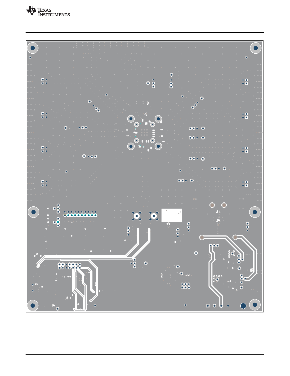
Figure 31. Bottom Composite View
SNAU236A–June 2018–Revised December 2018
Copyright © 2018, Texas Instruments Incorporated
Submit Documentation Feedback
Page 45

www.ti.com
6 EVM Bill of Materials
Table 12 lists the bill of materials.
REF DES QTY VALUE DESCRIPTION PART NUMBER MFR
!PCB1 1 Printed Circuit Board HSDC043 Any
C1, C2, C8,
C119, C120,
C122, C123,
C127, C130,
C131, C132
C3, C4 2 47uF
C5, C6, C7,
C125
C9, C10 2 10uF
C11, C12, C13,
C14, C55
C15, C16, C19,
C25, C30, C31,
C37, C38, C39,
C40, C41, C48,
C49, C50, C51,
C52, C53, C54,
C68, C69, C70,
C73, C78, C85,
C126, C129,
C135
C20, C26, C27,
C28, C29, C133
C21, C22, C32,
C33, C34, C35,
C36, C42, C43,
C44, C45, C46,
C47, C56, C76,
C80, C83, C84,
C90, C91, C92,
C93, C94, C95,
C96, C97, C98,
C99, C100,
C101, C102,
C103, C108,
C109, C110,
C134, C136,
R34, R35
C23, C24 2 0.47uF
C57, C58, C59,
C60, C61, C62,
C63, C64, C65,
C66, C67
C71, C77 2 3300pF
C72, C151 2 22uF
C75 1 0.033uF
C79 1 10uF
C82 1 0.1uF
11 0.1uF
4 22uF
5 1uF
27 10uF
6 0.01uF
39 0.1uF
11 0.1uF
Table 12. Bill of Materials
CAP, CERM, 0.1 uF, 16 V, +/- 5%,
X7R, 0603
CAP, CERM, 47 µF, 10 V,+/- 20%,
X5R, 0805
CAP, CERM, 22 uF, 10 V, +/- 20%,
X5R, 0805
CAP, CERM, 10 uF, 10 V, +/- 20%,
X7R, 1206
CAP, CERM, 1 uF, 10 V, +/- 10%,
X5R, 0603
CAP, CERM, 10 uF, 10 V, +/- 20%,
X5R, 0603
CAP, CERM, 0.01 uF, 50 V, +/- 5%,
X7R, 0603
CAP, CERM, 0.1 uF, 25 V, +/- 5%,
X7R, 0603
CAP, CERM, 0.47 uF, 10 V, +/- 10%,
X7R, 0603
CAP, CERM, 0.1 uF, 10 V, +/- 10%,
X5R, 0402
CAP, CERM, 3300 pF, 50 V, +/- 10%,
X7R, 0603
CAP, CERM, 22 uF, 10 V, +/- 20%,
X5R, 0603
CAP, CERM, 0.033 uF, 50 V, +/- 5%,
X7R, 0603
CAP, CERM, 10 uF, 10 V, +/- 10%,
X5R, 0805
CAP, CERM, 0.1 uF, 25 V, +/- 5%,
X7R, 0603S
EVM Bill of Materials
C0603C104J4RACTU Kemet
GRM21BR61A476ME15L MuRata
LMK212BJ226MG-T Taiyo Yuden
C3216X7R1A106M160AC TDK
C0603C105K8PACTU Kemet
C1608X5R1A106M080AC TDK
C0603C103J5RACTU Kemet
C0603C104J3RACTU Kemet
C0603C474K8RACTU Kemet
C1005X5R1A104K050BA TDK
C0603C332K5RACTU Kemet
C1608X5R1A226M080AC TDK
06035C333JAT2A AVX
LMK212BJ106KG-T Taiyo Yuden
C0603C104J3RACTU Kemet
SNAU236A–June 2018–Revised December 2018
Submit Documentation Feedback
Copyright © 2018, Texas Instruments Incorporated
LMK05318EVM User's Guide
45
Page 46

EVM Bill of Materials
REF DES QTY VALUE DESCRIPTION PART NUMBER MFR
C86, C87, C88,
C89, C104,
C105, R17, R18,
R19, R20, R21,
R22, R23, R24,
R25, R26, R27,
R37, R40, R41,
R45, R46, R47,
R48, R49, R56,
R57, R58, R59,
R60, R61, R62,
R63, R78, R79,
R80, R81, R96,
R97, R98, R99,
R114, R115,
R116, R117,
R138, R139,
R140, R141,
R159, R160,
R161, R162,
R163, R164,
R165, R166,
R172, R173,
R177, R178,
R179, R180,
R181, R182,
R184, R185,
R191
C114, C115 2 33pF
C116, C117 2 30pF
C118, C124 2 220pF
C121, C150 2 0.47uF
C128 1 2200pF
C139, C140,
C141, C142,
C143, C144,
C145, C146,
C147, C148,
C149
C152, C154 2 10uF
C153 1 0.47uF
C155, C156 2 22uF
C157, C158 2 47uF
D1, D2 2 20V Diode, Schottky, 20 V, 2 A, SMA B220A-13-F Diodes Inc.
D3, D4, D5,
D10, D13
D7, D8 2 Yellow LED, Yellow , SMD LTST-C170KSKT Lite-On
D9 1 7.5V Diode, Zener, 7.5 V, 550 mW, SMB 1SMB5922BT3G ON Semiconductor
D11 1 30V Diode, Schottky, 30 V, 0.2 A, SOT-23 BAT54-7-F Diodes Inc.
D12 1 Red LED, Red, SMD LTST-C170KRKT Lite-On
Table 12. Bill of Materials (continued)
68 0
11 1uF
5 Green LED, Green, SMD LTST-C190GKT Lite-On
RES, 0, 5%, 0.1 W, AEC-Q200 Grade
0, 0603
CAP, CERM, 33 pF, 100 V, +/- 5%,
C0G/NP0, 0603
CAP, CERM, 30 pF, 100 V, +/- 5%,
C0G/NP0, 0603
CAP, CERM, 220 pF, 50 V, +/- 1%,
C0G/NP0, 0603
CAP, CERM, 0.47 uF, 10 V, +/- 10%,
X7R, 0603
CAP, CERM, 2200 pF, 50 V, +/- 10%,
X7R, 0603
CAP, CERM, 1 uF, 6.3 V, +/- 20%,
X5R, 0402
CAP, CERM, 10 uF, 16 V, +/- 10%,
X5R, 0805
CAP, CERM, 0.47 uF, 10 V, +/- 10%,
X5R, 0402
CAP, CERM, 22 uF, 4 V, +/- 20%,
X6S, 0805
CAP, CERM, 47 uF, 6.3 V, +/- 10%,
X6S, 1206
CRCW06030000Z0EA Vishay-Dale
06031A330JAT2A AVX
GRM1885C2A300JA01D MuRata
06035A221FAT2A AVX
GRM188R71A474KA61D MuRata
C0603C222K5RACTU Kemet
GRM152R60J105ME15D MuRata
GRM21BR61C106KE15L MuRata
GRM155R61A474KE15D MuRata
GRM21BC80G226ME39L MuRata
GRM31CC80J476KE18L MuRata
www.ti.com
46
LMK05318EVM User's Guide
SNAU236A–June 2018–Revised December 2018
Submit Documentation Feedback
Copyright © 2018, Texas Instruments Incorporated
Page 47

www.ti.com
EVM Bill of Materials
Table 12. Bill of Materials (continued)
REF DES QTY VALUE DESCRIPTION PART NUMBER MFR
FB1, FB2, FB3,
FB4, FB5, FB6,
FB7, FB8, FB9,
FB10, FB11
FB12, FB14 2 300 ohm
FB13 1 60 ohm
H1, H2, H3, H4,
H5, H6
HS1, HS2, HS3,
HS4, HS5, HS6
J1 1 Terminal Block, 4x1, 5.08mm, TH 39544-3004 Molex
J2, J3, J6, J7,
J8, J9, J12, J13,
J14, J15, J18,
J19, J20, J21,
J24, J25, J26,
J27, J30, J31,
J32, J33
J4, J5 2
J35 1
JP1, JP2, JP3,
JP16, JP17,
JP18, JP19,
JP21, JP22,
JP23
JP4 1 Header, 100mil, 3x2, Gold, TH TSW-103-07-G-D Samtec
JP20 1 Header, 100mil, 7x2, Tin, TH PEC07DAAN
JT1, JT2, JT3,
JT4, JT5
L1, L2 2 2.2uH
LBL1 1
Q1, Q2, Q3, Q4 4 50V
Q5 1 25V
R1, R2 2 0.015 RES, 0.015, 1%, 0.5 W, 1206 CSR1206FK15L0
R3 1 0
R4, R5, R6 3 47k
R7 1 30.9k
R8 1 10.0k
R9 1 1.87k
R10 1 1.50k
R11 1 2.43k
11 220 ohm
6
6 Standoff, Hex, 0.5"L #4-40 Nylon 1902C Keystone
22
10 Header, 100mil, 3x1, Gold, TH TSW-103-07-G-S Samtec
5 Header, 100mil, 1pos, Gold, TH TSW-101-07-G-S Samtec
Ferrite Bead, 220 ohm @ 100 MHz,
2.5 A, 0603
Ferrite Bead, 300 ohm @ 100 MHz,
0.4 A, 1.6x0.8x0.95mm
Ferrite Bead, 60 ohm @ 100 MHz,
3.5 A, 0603
Machine Screw, Round, #4-40 x 1/4,
Nylon, Philips panhead
Connector, End launch SMA, 50 ohm,
SMT
SMA Straight PCB Socket Die Cast,
50 Ohm, TH
Connector, Receptacle, Mini-USB
Type B, R/A, Top Mount SMT
Inductor, Multilayer, Ferrite, 2.2 uH,
1.3 A, 0.08 ohm, SMD
Thermal Transfer Printable Labels,
0.650" W x 0.200" H - 10,000 per roll
MOSFET, N-CH, 50 V, 0.22 A, SOT-
23
MOSFET, N-CH, 25 V, 0.22 A, SOT-
23
RES, 0, 5%, 0.25 W, AEC-Q200
Grade 0, 1206
RES, 47 k, 5%, 0.1 W, AEC-Q200
Grade 0, 0603
RES, 30.9 k, 1%, 0.1 W, AEC-Q200
Grade 0, 0603
RES, 10.0 k, 1%, 0.1 W, AEC-Q200
Grade 0, 0603
RES, 1.87 k, 1%, 0.1 W, AEC-Q200
Grade 0, 0603
RES, 1.50 k, 1%, 0.1 W, AEC-Q200
Grade 0, 0603
RES, 2.43 k, 1%, 0.1 W, AEC-Q200
Grade 0, 0603
BLM18SG221TN1D MuRata
LI0603D301R-10
MPZ1608S600ATAH0 TDK
NY PMS 440 0025 PH
142-0701-851 Cinch Connectivity
5-1814832-1 TE Connectivity
1734035-2 TE Connectivity
LQM2HPN2R2MG0L MuRata
THT-14-423-10 Brady
BSS138
FDV301N
CRCW12060000Z0EA Vishay-Dale
CRCW060347K0JNEA Vishay-Dale
CRCW060330K9FKEA Vishay-Dale
CRCW060310K0FKEA Vishay-Dale
CRCW06031K87FKEA Vishay-Dale
CRCW06031K50FKEA Vishay-Dale
CRCW06032K43FKEA Vishay-Dale
Laird-Signal Integrity
Products
B&F Fastener
Supply
Sullins Connector
Solutions
Fairchild
Semiconductor
Fairchild
Semiconductor
Stackpole
Electronics Inc
SNAU236A–June 2018–Revised December 2018
Submit Documentation Feedback
Copyright © 2018, Texas Instruments Incorporated
LMK05318EVM User's Guide
47
Page 48

EVM Bill of Materials
REF DES QTY VALUE DESCRIPTION PART NUMBER MFR
R12, R14, R16 3 1.15k
R13, R15 2 3.57k RES, 3.57 k, 1%, 0.1 W, 0603 RC0603FR-073K57L Yageo
R28, R29, R31,
R132, R133,
R194, R195
R30, R42, R134,
R135, R136,
R137, R142,
R143, R144,
R146, R147,
R154
R32 1 5.11
R33, R156 2 100
R36, R44 2 49.9k
R38, R39 2 49.9
R145, R150,
R153
R148, R151,
R157, R174,
R175, R197
R149, R158,
R183
R167, R176,
R186
R168, R169 2 33
R170 1 1.5k
R171 1 1.2Meg
R187, R188,
R189
R190, R192 2 1.5k
R193 1 100k
R198, R199 2 150
R200, R201 2 9.76k
R202 1 12.7k
R203, R205 2 10.2k
R204 1 32.4k RES, 32.4 k, 1%, 0.1 W, 0603 RC0603FR-0732K4L Yageo
S1, S2, S3 3
S4, S8 2
S5, S6, S7 3 Switch, Slide, SPST 3 poles, SMT 219-3LPST
7 470
12 10k
3 3.9k
6 1.0k
3 100
3 33k
3 510
Table 12. Bill of Materials (continued)
RES, 1.15 k, 1%, 0.1 W, AEC-Q200
Grade 0, 0603
RES, 470, 5%, 0.1 W, AEC-Q200
Grade 0, 0603
RES, 10 k, 5%, 0.1 W, AEC-Q200
Grade 0, 0603
RES, 5.11, 1%, 0.063 W, AEC-Q200
Grade 0, 0402
RES, 100, 5%, 0.25 W, AEC-Q200
Grade 0, 0603
RES, 49.9 k, 1%, 0.063 W, AECQ200 Grade 0, 0402
RES, 49.9, 1%, 0.1 W, AEC-Q200
Grade 0, 0603
RES, 3.9 k, 5%, 0.1 W, AEC-Q200
Grade 0, 0603
RES, 1.0 k, 5%, 0.1 W, AEC-Q200
Grade 0, 0603
RES, 100, 5%, 0.1 W, AEC-Q200
Grade 0, 0603
RES, 33 k, 5%, 0.1 W, AEC-Q200
Grade 0, 0603
RES, 33, 5%, 0.063 W, AEC-Q200
Grade 0, 0402
RES, 1.5 k, 5%, 0.063 W, AEC-Q200
Grade 0, 0402
RES, 1.2 M, 5%, 0.1 W, AEC-Q200
Grade 0, 0603
RES, 510, 5%, 0.1 W, AEC-Q200
Grade 0, 0603
RES, 1.5 k, 5%, 0.1 W, AEC-Q200
Grade 0, 0603
RES, 100 k, 5%, 0.1 W, AEC-Q200
Grade 0, 0603
RES, 150, 5%, 0.1 W, AEC-Q200
Grade 0, 0603
RES, 9.76 k, 1%, 0.063 W, AECQ200 Grade 0, 0402
RES, 12.7 k, 1%, 0.063 W, AECQ200 Grade 0, 0402
RES, 10.2 k, 1%, 0.063 W, AECQ200 Grade 0, 0402
Switch, SPST 4 Pos, Top Actuated,
SMT
Switch, Tactile, SPST-NO, 0.05A,
12V, SMT
CRCW06031K15FKEA Vishay-Dale
CRCW0603470RJNEA Vishay-Dale
CRCW060310K0JNEA Vishay-Dale
CRCW04025R11FKED Vishay-Dale
ESR03EZPJ101 Rohm
CRCW040249K9FKED Vishay-Dale
CRCW060349R9FKEA Vishay-Dale
CRCW06033K90JNEA Vishay-Dale
CRCW06031K00JNEA Vishay-Dale
CRCW0603100RJNEA Vishay-Dale
CRCW060333K0JNEA Vishay-Dale
CRCW040233R0JNED Vishay-Dale
CRCW04021K50JNED Vishay-Dale
CRCW06031M20JNEA Vishay-Dale
CRCW0603510RJNEA Vishay-Dale
CRCW06031K50JNEA Vishay-Dale
CRCW0603100KJNEA Vishay-Dale
CRCW0603150RJNEA Vishay-Dale
CRCW04029K76FKED Vishay-Dale
CRCW040212K7FKED Vishay-Dale
CRCW040210K2FKED Vishay-Dale
219-4LPST
FSM4JSMA TE Connectivity
www.ti.com
CTS
Electrocomponents
CTS
Electrocomponents
48
LMK05318EVM User's Guide
SNAU236A–June 2018–Revised December 2018
Submit Documentation Feedback
Copyright © 2018, Texas Instruments Incorporated
Page 49

www.ti.com
EVM Bill of Materials
Table 12. Bill of Materials (continued)
REF DES QTY VALUE DESCRIPTION PART NUMBER MFR
S9 1
S10 1 Switch, Slide, SPST 2 poles, SMT 219-2LPST
SH1, SH2, SH3,
SH4, SH5, SH6,
SH7, SH8, SH9,
SH10, SH11,
SH12, SH13,
SH14, SH15
TP1, TP2, TP3,
TP4, TP5, TP6,
TP7, TP25
TP23, TP24,
TP26, TP27
U1, U2 2
U3 1
U4 1
U5 1
U6 1
U7 1
U8 1
U9 1
U10 1
U11 1
Y1 1 OSC, 48.004800 MHz, 3.3V, SMD 8W48070002 TXC Corporation
Y2 1 Crystal, 24.000 MHz, 20pF, SMD ECS-240-20-5PX-TR ECS Inc.
C17, C18 0 0.01uF
C74, C81, C137,
C138
C106, C107,
C111, C112,
C113
15 1x2 Shunt, 100mil, Gold plated, Black SNT-100-BK-G Samtec
8 Test Point, Miniature, Red, TH 5000 Keystone
4 Test Point, Miniature, Black, TH 5001 Keystone
0 0.1uF
0 100pF
Switch, SPST, Slide, Off-On, 2 Pos,
0.1A, 20V, SMD
26-V, Bi-Directional, Zero-Drift, High
Accuracy, Low-/High-Side, Voltage
Out Current Shunt Monitor,
DCK0006A (SOT-SC70-6)
Dual 1A Low-Noise (3.8µVRMS) LDO
Voltage Regulator, RTJ0020D
(WQFN-20)
Low-Noise, High-Bandwidth PSRR,
Low-Dropout 1-A Linear Regulator,
DRB0008A (VSON-8)
Ultra-Low Jitter Clock Synchronizer
and Jitter Cleaner with Two
Frequency Domains, Eight Differential
Outputs, Two Differential Inputs,
RGZ0048N (VQFN-48)
4-Channel ESD Protection Array for
High-Speed Data Interfaces,
DRY0006A (USON-6)
25 MHz Mixed Signal Microcontroller
with 128 KB Flash, 8192 B SRAM
and 63 GPIOs, -40 to 85 degC, 80-pin
QFP (PN), Green (RoHS and no
Sb/Br)
150-mA Ultra-Low Noise LDO for RF
and Analog Circuits Requires No
Bypass Capacitor, NGF0006A
(WSON-6)
Single 2-Input Exclusive-OR Gate,
DBV0005A (SOT-23-5)
Ultra-Low Jitter Fully Programmable
Oscillator, Integrated EEPROM, +/50ppm, SIA0008B (QFM-8)
Dual 2.0A, High-frequency
Synchronous Step-Down DC-DC
Regulator, RUM0016A (WQFN-16)
CAP, CERM, 0.01 uF, 50 V, +/- 5%,
X7R, 0603
CAP, CERM, 0.1 uF, 25 V, +/- 5%,
X7R, 0603
CAP, CERM, 100 pF, 50 V, +/- 5%,
C0G/NP0, 0603
219-2MST
INA214AIDCKR Texas Instruments
TPS7A8801RTJR Texas Instruments
TPS7A8101DRBR Texas Instruments
LMK05318RGZR Texas Instruments
TPD4E004DRYR Texas Instruments
MSP430F5529IPN Texas Instruments
LP5900SD-3.3/NOPB Texas Instruments
SN74LVC1G86DBVR Texas Instruments
LMK61E2-SIAR Texas Instruments
LM26420XSQX/NOPB Texas Instruments
C0603C103J5RACTU Kemet
C0603C104J3RACTU Kemet
06035A101JAT2A AVX
CTS
Electrocomponents
CTS
Electrocomponents
SNAU236A–June 2018–Revised December 2018
Submit Documentation Feedback
Copyright © 2018, Texas Instruments Incorporated
LMK05318EVM User's Guide
49
Page 50

EVM Bill of Materials
REF DES QTY VALUE DESCRIPTION PART NUMBER MFR
FID1, FID2,
FID3, FID4,
FID5, FID6
J10, J11, J16,
J17, J22, J23,
J28, J29
J34 0 Header, 2.54mm, 10x2, Tin, TH 929836-04-10-RK 3M
JP5, JP6, JP7,
JP8, JP9, JP10,
JP11, JP12,
JP13, JP14,
JP15
R43, R196 0 10k
R50, R51, R52,
R53, R64, R65,
R66, R67, R74,
R75, R76, R77,
R82, R83, R84,
R85, R92, R93,
R94, R95, R100,
R101, R102,
R103, R110,
R111, R112,
R113, R118,
R119, R120,
R121, R128,
R129, R130,
R131
R54, R55 0 100
R68, R70, R71,
R73, R86, R88,
R89, R91, R104,
R106, R107,
R109, R122,
R124, R125,
R127
R69, R72, R87,
R90, R105,
R108, R123,
R126
R152, R155 0 1.0k
TP8, TP9, TP10,
TP11, TP12,
TP13, TP14,
TP15, TP16,
TP17, TP18,
TP33
TP19, TP20,
TP21, TP22
XU1 0 Socket, QFN-48, 0.5 mm, SMT 106458-0020 HSIO Technologies
Table 12. Bill of Materials (continued)
0
0 Header, 100mil, 2x2, Tin, TH PEC02DAAN
0 Header, 100mil, 3x1, Gold, TH TSW-103-07-G-S Samtec
0 49.9
0 0
0 100
0 Test Point, Miniature, Red, TH 5000 Keystone
0 Test Point, Miniature, Black, TH 5001 Keystone
Fiducial mark. There is nothing to buy
or mount.
RES, 10 k, 5%, 0.1 W, AEC-Q200
Grade 0, 0603
RES, 49.9, 1%, 0.1 W, AEC-Q200
Grade 0, 0603
RES, 100, 1%, 0.1 W, AEC-Q200
Grade 0, 0603
RES, 0, 5%, 0.1 W, AEC-Q200 Grade
0, 0603
RES, 100, 5%, 0.1 W, AEC-Q200
Grade 0, 0603
RES, 1.0 k, 5%, 0.1 W, AEC-Q200
Grade 0, 0603
N/A N/A
Sullins Connector
Solutions
CRCW060310K0JNEA Vishay-Dale
CRCW060349R9FKEA Vishay-Dale
CRCW0603100RFKEA Vishay-Dale
CRCW06030000Z0EA Vishay-Dale
CRCW0603100RJNEA Vishay-Dale
CRCW06031K00JNEA Vishay-Dale
www.ti.com
50
LMK05318EVM User's Guide
Copyright © 2018, Texas Instruments Incorporated
SNAU236A–June 2018–Revised December 2018
Submit Documentation Feedback
Page 51

A.1 Software Installation (One-Time)
1. Download and Install TICS Pro Software GUI v1.6.9 (or later) from here.
2. Download and Install MATLAB Runtime v9.0 (2015b, 64-bit).
a. Download the installer here
b. This is required to run the compiled Matlab script bundled with the device profile.
3. Reboot the PC for proper installation of MATLAB Runtime, if needed.
4. Launch TICS Pro.
A.2 TICS Pro Usage for LMK05318
1. Launch TICS Pro.
2. Connect the PC to the EVM with the USB cable.
3. Confirm switches S9[1:2] are OFF on the EVM so only the LMK05318 is found when the I2C bus is
scanned.
4. Select the LMK05318 profile, if needed: Click Select Device > Network Synchronizer Clock (Digital
PLLs) > LMK05318
5. Click USB communication > Interface.
a. Under Interface, tick USB2ANY.
b. Select Protocol: I2C or SPI_CLKLOW.
c. Follow the Change Device Mode & Protocol dialog:
i. On the EVM, set JP19 and JP20 jumpers accordingly for I2C or SPI Mode.
ii. Click Yes to confirm change or No to cancel.
d. Press Close to apply the Mode & Protocol changes.
6. Follow the dialogs:
a. Scan I2C Bus – Yes to confirm, No to skip.
• LMK05318 should be found at 0x64, 0x65, or 0x66 depending on the GPIO1/SCS input level
(set by S6 or MCU control).
• If the scan found a device at 0x58, it is probably U7 (LMK61E2). In this case, restart from Step
3 to find the LMK05318.
• Alternatively, in the Communication setup window (Step 5), manually enter the I2C address as
0x64, 0x65, or 0x66 and click Set I2C Address.
b. Write All Registers – Yes to confirm, No to skip.
7. Follow the step-by-step procedure on the Start Page to enter the clock design parameters, run the
script to generate the DPLL-specific register settings, and program the device registers.
a. See the Detailed Design Procedure section of the LMK05318 data sheet for additional help on the
device configuration using TICS Pro.
b. After all registers are programmed, a soft reset can be triggered to restart the device (soft reset
does not reset the active registers).
When the desired device functionality and performance has been confirmed, the active configuration can
be programmed to the EEPROM to allow auto-startup on the next power cycle.
Appendix A
SNAU236A–June 2018–Revised December 2018
Software
SNAU236A–June 2018–Revised December 2018
Submit Documentation Feedback
Copyright © 2018, Texas Instruments Incorporated
Software
51
Page 52

Revision History
www.ti.com
Revision History
NOTE: Page numbers for previous revisions may differ from page numbers in the current version.
Changes from Original (June 2018) to A Revision ......................................................................................................... Page
• Changed the setting descriptions in the Default Jumper and DIP Switch Settings table ........................................ 7
• Added Device Revision Identification section ......................................................................................... 8
• Updated the Default Configuration - EEPROM Start-Up Modes table ............................................................. 9
• Added design suggestions whille using EEPROM mode in the Device Start-Up Modes section............................. 10
• Updated the Key EVM Components table............................................................................................ 11
• Updated the Logic Pin Mapping tables ............................................................................................... 15
• Updated the Bill of Materials table..................................................................................................... 45
• Removed steps in the Software Installation (One-Time) instructions............................................................. 51
• Added information to the TICS Pro Usage for LMK05318 set of instructions ................................................... 51
52
Revision History
Copyright © 2018, Texas Instruments Incorporated
SNAU236A–June 2018–Revised December 2018
Submit Documentation Feedback
Page 53

STANDARD TERMS FOR EVALUATION MODULES
1. Delivery: TI delivers TI evaluation boards, kits, or modules, including any accompanying demonstration software, components, and/or
documentation which may be provided together or separately (collectively, an “EVM” or “EVMs”) to the User (“User”) in accordance
with the terms set forth herein. User's acceptance of the EVM is expressly subject to the following terms.
1.1 EVMs are intended solely for product or software developers for use in a research and development setting to facilitate feasibility
evaluation, experimentation, or scientific analysis of TI semiconductors products. EVMs have no direct function and are not
finished products. EVMs shall not be directly or indirectly assembled as a part or subassembly in any finished product. For
clarification, any software or software tools provided with the EVM (“Software”) shall not be subject to the terms and conditions
set forth herein but rather shall be subject to the applicable terms that accompany such Software
1.2 EVMs are not intended for consumer or household use. EVMs may not be sold, sublicensed, leased, rented, loaned, assigned,
or otherwise distributed for commercial purposes by Users, in whole or in part, or used in any finished product or production
system.
2 Limited Warranty and Related Remedies/Disclaimers:
2.1 These terms do not apply to Software. The warranty, if any, for Software is covered in the applicable Software License
Agreement.
2.2 TI warrants that the TI EVM will conform to TI's published specifications for ninety (90) days after the date TI delivers such EVM
to User. Notwithstanding the foregoing, TI shall not be liable for a nonconforming EVM if (a) the nonconformity was caused by
neglect, misuse or mistreatment by an entity other than TI, including improper installation or testing, or for any EVMs that have
been altered or modified in any way by an entity other than TI, (b) the nonconformity resulted from User's design, specifications
or instructions for such EVMs or improper system design, or (c) User has not paid on time. Testing and other quality control
techniques are used to the extent TI deems necessary. TI does not test all parameters of each EVM.
User's claims against TI under this Section 2 are void if User fails to notify TI of any apparent defects in the EVMs within ten (10)
business days after delivery, or of any hidden defects with ten (10) business days after the defect has been detected.
2.3 TI's sole liability shall be at its option to repair or replace EVMs that fail to conform to the warranty set forth above, or credit
User's account for such EVM. TI's liability under this warranty shall be limited to EVMs that are returned during the warranty
period to the address designated by TI and that are determined by TI not to conform to such warranty. If TI elects to repair or
replace such EVM, TI shall have a reasonable time to repair such EVM or provide replacements. Repaired EVMs shall be
warranted for the remainder of the original warranty period. Replaced EVMs shall be warranted for a new full ninety (90) day
warranty period.
3 Regulatory Notices:
3.1 United States
3.1.1 Notice applicable to EVMs not FCC-Approved:
FCC NOTICE: This kit is designed to allow product developers to evaluate electronic components, circuitry, or software
associated with the kit to determine whether to incorporate such items in a finished product and software developers to write
software applications for use with the end product. This kit is not a finished product and when assembled may not be resold or
otherwise marketed unless all required FCC equipment authorizations are first obtained. Operation is subject to the condition
that this product not cause harmful interference to licensed radio stations and that this product accept harmful interference.
Unless the assembled kit is designed to operate under part 15, part 18 or part 95 of this chapter, the operator of the kit must
operate under the authority of an FCC license holder or must secure an experimental authorization under part 5 of this chapter.
3.1.2 For EVMs annotated as FCC – FEDERAL COMMUNICATIONS COMMISSION Part 15 Compliant:
CAUTION
This device complies with part 15 of the FCC Rules. Operation is subject to the following two conditions: (1) This device may not
cause harmful interference, and (2) this device must accept any interference received, including interference that may cause
undesired operation.
Changes or modifications not expressly approved by the party responsible for compliance could void the user's authority to
operate the equipment.
FCC Interference Statement for Class A EVM devices
NOTE: This equipment has been tested and found to comply with the limits for a Class A digital device, pursuant to part 15 of
the FCC Rules. These limits are designed to provide reasonable protection against harmful interference when the equipment is
operated in a commercial environment. This equipment generates, uses, and can radiate radio frequency energy and, if not
installed and used in accordance with the instruction manual, may cause harmful interference to radio communications.
Operation of this equipment in a residential area is likely to cause harmful interference in which case the user will be required to
correct the interference at his own expense.
Page 54

FCC Interference Statement for Class B EVM devices
NOTE: This equipment has been tested and found to comply with the limits for a Class B digital device, pursuant to part 15 of
the FCC Rules. These limits are designed to provide reasonable protection against harmful interference in a residential
installation. This equipment generates, uses and can radiate radio frequency energy and, if not installed and used in accordance
with the instructions, may cause harmful interference to radio communications. However, there is no guarantee that interference
will not occur in a particular installation. If this equipment does cause harmful interference to radio or television reception, which
can be determined by turning the equipment off and on, the user is encouraged to try to correct the interference by one or more
of the following measures:
• Reorient or relocate the receiving antenna.
• Increase the separation between the equipment and receiver.
• Connect the equipment into an outlet on a circuit different from that to which the receiver is connected.
• Consult the dealer or an experienced radio/TV technician for help.
3.2 Canada
3.2.1 For EVMs issued with an Industry Canada Certificate of Conformance to RSS-210 or RSS-247
Concerning EVMs Including Radio Transmitters:
This device complies with Industry Canada license-exempt RSSs. Operation is subject to the following two conditions:
(1) this device may not cause interference, and (2) this device must accept any interference, including interference that may
cause undesired operation of the device.
Concernant les EVMs avec appareils radio:
Le présent appareil est conforme aux CNR d'Industrie Canada applicables aux appareils radio exempts de licence. L'exploitation
est autorisée aux deux conditions suivantes: (1) l'appareil ne doit pas produire de brouillage, et (2) l'utilisateur de l'appareil doit
accepter tout brouillage radioélectrique subi, même si le brouillage est susceptible d'en compromettre le fonctionnement.
Concerning EVMs Including Detachable Antennas:
Under Industry Canada regulations, this radio transmitter may only operate using an antenna of a type and maximum (or lesser)
gain approved for the transmitter by Industry Canada. To reduce potential radio interference to other users, the antenna type
and its gain should be so chosen that the equivalent isotropically radiated power (e.i.r.p.) is not more than that necessary for
successful communication. This radio transmitter has been approved by Industry Canada to operate with the antenna types
listed in the user guide with the maximum permissible gain and required antenna impedance for each antenna type indicated.
Antenna types not included in this list, having a gain greater than the maximum gain indicated for that type, are strictly prohibited
for use with this device.
Concernant les EVMs avec antennes détachables
Conformément à la réglementation d'Industrie Canada, le présent émetteur radio peut fonctionner avec une antenne d'un type et
d'un gain maximal (ou inférieur) approuvé pour l'émetteur par Industrie Canada. Dans le but de réduire les risques de brouillage
radioélectrique à l'intention des autres utilisateurs, il faut choisir le type d'antenne et son gain de sorte que la puissance isotrope
rayonnée équivalente (p.i.r.e.) ne dépasse pas l'intensité nécessaire à l'établissement d'une communication satisfaisante. Le
présent émetteur radio a été approuvé par Industrie Canada pour fonctionner avec les types d'antenne énumérés dans le
manuel d’usage et ayant un gain admissible maximal et l'impédance requise pour chaque type d'antenne. Les types d'antenne
non inclus dans cette liste, ou dont le gain est supérieur au gain maximal indiqué, sont strictement interdits pour l'exploitation de
l'émetteur
3.3 Japan
3.3.1 Notice for EVMs delivered in Japan: Please see http://www.tij.co.jp/lsds/ti_ja/general/eStore/notice_01.page 日本国内に
輸入される評価用キット、ボードについては、次のところをご覧ください。
http://www.tij.co.jp/lsds/ti_ja/general/eStore/notice_01.page
3.3.2 Notice for Users of EVMs Considered “Radio Frequency Products” in Japan: EVMs entering Japan may not be certified
by TI as conforming to Technical Regulations of Radio Law of Japan.
If User uses EVMs in Japan, not certified to Technical Regulations of Radio Law of Japan, User is required to follow the
instructions set forth by Radio Law of Japan, which includes, but is not limited to, the instructions below with respect to EVMs
(which for the avoidance of doubt are stated strictly for convenience and should be verified by User):
1. Use EVMs in a shielded room or any other test facility as defined in the notification #173 issued by Ministry of Internal
Affairs and Communications on March 28, 2006, based on Sub-section 1.1 of Article 6 of the Ministry’s Rule for
Enforcement of Radio Law of Japan,
2. Use EVMs only after User obtains the license of Test Radio Station as provided in Radio Law of Japan with respect to
EVMs, or
3. Use of EVMs only after User obtains the Technical Regulations Conformity Certification as provided in Radio Law of Japan
with respect to EVMs. Also, do not transfer EVMs, unless User gives the same notice above to the transferee. Please note
that if User does not follow the instructions above, User will be subject to penalties of Radio Law of Japan.
Page 55

【無線電波を送信する製品の開発キットをお使いになる際の注意事項】 開発キットの中には技術基準適合証明を受けて
いないものがあります。 技術適合証明を受けていないもののご使用に際しては、電波法遵守のため、以下のいずれかの
措置を取っていただく必要がありますのでご注意ください。
1. 電波法施行規則第6条第1項第1号に基づく平成18年3月28日総務省告示第173号で定められた電波暗室等の試験設備でご使用
いただく。
2. 実験局の免許を取得後ご使用いただく。
3. 技術基準適合証明を取得後ご使用いただく。
なお、本製品は、上記の「ご使用にあたっての注意」を譲渡先、移転先に通知しない限り、譲渡、移転できないものとします。
上記を遵守頂けない場合は、電波法の罰則が適用される可能性があることをご留意ください。 日本テキサス・イ
ンスツルメンツ株式会社
東京都新宿区西新宿6丁目24番1号
西新宿三井ビル
3.3.3 Notice for EVMs for Power Line Communication: Please see http://www.tij.co.jp/lsds/ti_ja/general/eStore/notice_02.page
電力線搬送波通信についての開発キットをお使いになる際の注意事項については、次のところをご覧ください。http:/
/www.tij.co.jp/lsds/ti_ja/general/eStore/notice_02.page
3.4 European Union
3.4.1 For EVMs subject to EU Directive 2014/30/EU (Electromagnetic Compatibility Directive):
This is a class A product intended for use in environments other than domestic environments that are connected to a
low-voltage power-supply network that supplies buildings used for domestic purposes. In a domestic environment this
product may cause radio interference in which case the user may be required to take adequate measures.
4 EVM Use Restrictions and Warnings:
4.1 EVMS ARE NOT FOR USE IN FUNCTIONAL SAFETY AND/OR SAFETY CRITICAL EVALUATIONS, INCLUDING BUT NOT
LIMITED TO EVALUATIONS OF LIFE SUPPORT APPLICATIONS.
4.2 User must read and apply the user guide and other available documentation provided by TI regarding the EVM prior to handling
or using the EVM, including without limitation any warning or restriction notices. The notices contain important safety information
related to, for example, temperatures and voltages.
4.3 Safety-Related Warnings and Restrictions:
4.3.1 User shall operate the EVM within TI’s recommended specifications and environmental considerations stated in the user
guide, other available documentation provided by TI, and any other applicable requirements and employ reasonable and
customary safeguards. Exceeding the specified performance ratings and specifications (including but not limited to input
and output voltage, current, power, and environmental ranges) for the EVM may cause personal injury or death, or
property damage. If there are questions concerning performance ratings and specifications, User should contact a TI
field representative prior to connecting interface electronics including input power and intended loads. Any loads applied
outside of the specified output range may also result in unintended and/or inaccurate operation and/or possible
permanent damage to the EVM and/or interface electronics. Please consult the EVM user guide prior to connecting any
load to the EVM output. If there is uncertainty as to the load specification, please contact a TI field representative.
During normal operation, even with the inputs and outputs kept within the specified allowable ranges, some circuit
components may have elevated case temperatures. These components include but are not limited to linear regulators,
switching transistors, pass transistors, current sense resistors, and heat sinks, which can be identified using the
information in the associated documentation. When working with the EVM, please be aware that the EVM may become
very warm.
4.3.2 EVMs are intended solely for use by technically qualified, professional electronics experts who are familiar with the
dangers and application risks associated with handling electrical mechanical components, systems, and subsystems.
User assumes all responsibility and liability for proper and safe handling and use of the EVM by User or its employees,
affiliates, contractors or designees. User assumes all responsibility and liability to ensure that any interfaces (electronic
and/or mechanical) between the EVM and any human body are designed with suitable isolation and means to safely
limit accessible leakage currents to minimize the risk of electrical shock hazard. User assumes all responsibility and
liability for any improper or unsafe handling or use of the EVM by User or its employees, affiliates, contractors or
designees.
4.4 User assumes all responsibility and liability to determine whether the EVM is subject to any applicable international, federal,
state, or local laws and regulations related to User’s handling and use of the EVM and, if applicable, User assumes all
responsibility and liability for compliance in all respects with such laws and regulations. User assumes all responsibility and
liability for proper disposal and recycling of the EVM consistent with all applicable international, federal, state, and local
requirements.
5. Accuracy of Information: To the extent TI provides information on the availability and function of EVMs, TI attempts to be as accurate
as possible. However, TI does not warrant the accuracy of EVM descriptions, EVM availability or other information on its websites as
accurate, complete, reliable, current, or error-free.
Page 56

6. Disclaimers:
6.1 EXCEPT AS SET FORTH ABOVE, EVMS AND ANY MATERIALS PROVIDED WITH THE EVM (INCLUDING, BUT NOT
LIMITED TO, REFERENCE DESIGNS AND THE DESIGN OF THE EVM ITSELF) ARE PROVIDED "AS IS" AND "WITH ALL
FAULTS." TI DISCLAIMS ALL OTHER WARRANTIES, EXPRESS OR IMPLIED, REGARDING SUCH ITEMS, INCLUDING BUT
NOT LIMITED TO ANY EPIDEMIC FAILURE WARRANTY OR IMPLIED WARRANTIES OF MERCHANTABILITY OR FITNESS
FOR A PARTICULAR PURPOSE OR NON-INFRINGEMENT OF ANY THIRD PARTY PATENTS, COPYRIGHTS, TRADE
SECRETS OR OTHER INTELLECTUAL PROPERTY RIGHTS.
6.2 EXCEPT FOR THE LIMITED RIGHT TO USE THE EVM SET FORTH HEREIN, NOTHING IN THESE TERMS SHALL BE
CONSTRUED AS GRANTING OR CONFERRING ANY RIGHTS BY LICENSE, PATENT, OR ANY OTHER INDUSTRIAL OR
INTELLECTUAL PROPERTY RIGHT OF TI, ITS SUPPLIERS/LICENSORS OR ANY OTHER THIRD PARTY, TO USE THE
EVM IN ANY FINISHED END-USER OR READY-TO-USE FINAL PRODUCT, OR FOR ANY INVENTION, DISCOVERY OR
IMPROVEMENT, REGARDLESS OF WHEN MADE, CONCEIVED OR ACQUIRED.
7. USER'S INDEMNITY OBLIGATIONS AND REPRESENTATIONS. USER WILL DEFEND, INDEMNIFY AND HOLD TI, ITS
LICENSORS AND THEIR REPRESENTATIVES HARMLESS FROM AND AGAINST ANY AND ALL CLAIMS, DAMAGES, LOSSES,
EXPENSES, COSTS AND LIABILITIES (COLLECTIVELY, "CLAIMS") ARISING OUT OF OR IN CONNECTION WITH ANY
HANDLING OR USE OF THE EVM THAT IS NOT IN ACCORDANCE WITH THESE TERMS. THIS OBLIGATION SHALL APPLY
WHETHER CLAIMS ARISE UNDER STATUTE, REGULATION, OR THE LAW OF TORT, CONTRACT OR ANY OTHER LEGAL
THEORY, AND EVEN IF THE EVM FAILS TO PERFORM AS DESCRIBED OR EXPECTED.
8. Limitations on Damages and Liability:
8.1 General Limitations. IN NO EVENT SHALL TI BE LIABLE FOR ANY SPECIAL, COLLATERAL, INDIRECT, PUNITIVE,
INCIDENTAL, CONSEQUENTIAL, OR EXEMPLARY DAMAGES IN CONNECTION WITH OR ARISING OUT OF THESE
TERMS OR THE USE OF THE EVMS , REGARDLESS OF WHETHER TI HAS BEEN ADVISED OF THE POSSIBILITY OF
SUCH DAMAGES. EXCLUDED DAMAGES INCLUDE, BUT ARE NOT LIMITED TO, COST OF REMOVAL OR
REINSTALLATION, ANCILLARY COSTS TO THE PROCUREMENT OF SUBSTITUTE GOODS OR SERVICES, RETESTING,
OUTSIDE COMPUTER TIME, LABOR COSTS, LOSS OF GOODWILL, LOSS OF PROFITS, LOSS OF SAVINGS, LOSS OF
USE, LOSS OF DATA, OR BUSINESS INTERRUPTION. NO CLAIM, SUIT OR ACTION SHALL BE BROUGHT AGAINST TI
MORE THAN TWELVE (12) MONTHS AFTER THE EVENT THAT GAVE RISE TO THE CAUSE OF ACTION HAS
OCCURRED.
8.2 Specific Limitations. IN NO EVENT SHALL TI'S AGGREGATE LIABILITY FROM ANY USE OF AN EVM PROVIDED
HEREUNDER, INCLUDING FROM ANY WARRANTY, INDEMITY OR OTHER OBLIGATION ARISING OUT OF OR IN
CONNECTION WITH THESE TERMS, , EXCEED THE TOTAL AMOUNT PAID TO TI BY USER FOR THE PARTICULAR
EVM(S) AT ISSUE DURING THE PRIOR TWELVE (12) MONTHS WITH RESPECT TO WHICH LOSSES OR DAMAGES ARE
CLAIMED. THE EXISTENCE OF MORE THAN ONE CLAIM SHALL NOT ENLARGE OR EXTEND THIS LIMIT.
9. Return Policy. Except as otherwise provided, TI does not offer any refunds, returns, or exchanges. Furthermore, no return of EVM(s)
will be accepted if the package has been opened and no return of the EVM(s) will be accepted if they are damaged or otherwise not in
a resalable condition. If User feels it has been incorrectly charged for the EVM(s) it ordered or that delivery violates the applicable
order, User should contact TI. All refunds will be made in full within thirty (30) working days from the return of the components(s),
excluding any postage or packaging costs.
10. Governing Law: These terms and conditions shall be governed by and interpreted in accordance with the laws of the State of Texas,
without reference to conflict-of-laws principles. User agrees that non-exclusive jurisdiction for any dispute arising out of or relating to
these terms and conditions lies within courts located in the State of Texas and consents to venue in Dallas County, Texas.
Notwithstanding the foregoing, any judgment may be enforced in any United States or foreign court, and TI may seek injunctive relief
in any United States or foreign court.
Mailing Address: Texas Instruments, Post Office Box 655303, Dallas, Texas 75265
Copyright © 2018, Texas Instruments Incorporated
Page 57

IMPORTANT NOTICE AND DISCLAIMER
TI PROVIDES TECHNICAL AND RELIABILITY DATA (INCLUDING DATASHEETS), DESIGN RESOURCES (INCLUDING REFERENCE
DESIGNS), APPLICATION OR OTHER DESIGN ADVICE, WEB TOOLS, SAFETY INFORMATION, AND OTHER RESOURCES “AS IS”
AND WITH ALL FAULTS, AND DISCLAIMS ALL WARRANTIES, EXPRESS AND IMPLIED, INCLUDING WITHOUT LIMITATION ANY
IMPLIED WARRANTIES OF MERCHANTABILITY, FITNESS FOR A PARTICULAR PURPOSE OR NON-INFRINGEMENT OF THIRD
PARTY INTELLECTUAL PROPERTY RIGHTS.
These resources are intended for skilled developers designing with TI products. You are solely responsible for (1) selecting the appropriate
TI products for your application, (2) designing, validating and testing your application, and (3) ensuring your application meets applicable
standards, and any other safety, security, or other requirements. These resources are subject to change without notice. TI grants you
permission to use these resources only for development of an application that uses the TI products described in the resource. Other
reproduction and display of these resources is prohibited. No license is granted to any other TI intellectual property right or to any third
party intellectual property right. TI disclaims responsibility for, and you will fully indemnify TI and its representatives against, any claims,
damages, costs, losses, and liabilities arising out of your use of these resources.
TI’s products are provided subject to TI’s Terms of Sale (www.ti.com/legal/termsofsale.html) or other applicable terms available either on
ti.com or provided in conjunction with such TI products. TI’s provision of these resources does not expand or otherwise alter TI’s applicable
warranties or warranty disclaimers for TI products.
Mailing Address: Texas Instruments, Post Office Box 655303, Dallas, Texas 75265
Copyright © 2018, Texas Instruments Incorporated
 Loading...