

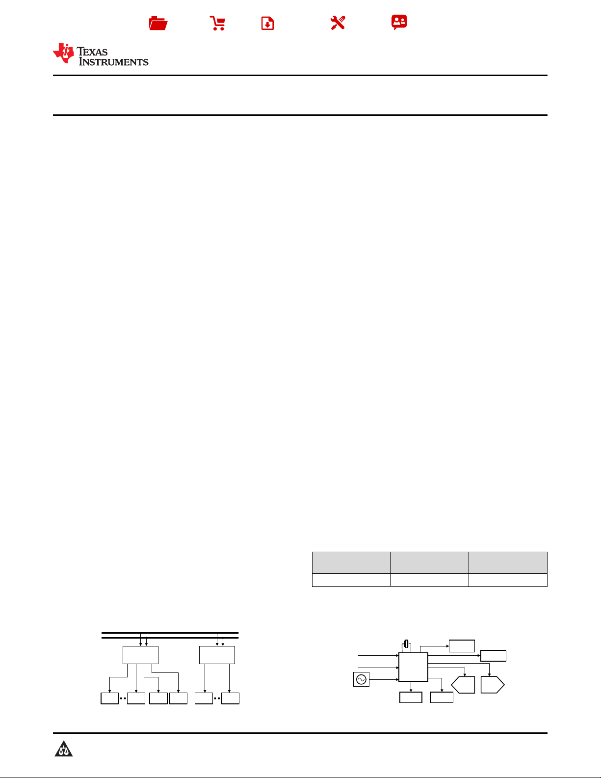
LMK04906 LMK04906
10 GbE
PHY
10 GbE
PHY
FPGA NPU SONET SONET
622.08,
155.52, 77.76,
19.44 MHz
Hitless Switching, Jitter
Cleaning, Frequency
Multiplication, and
Programmable Clock
Distribution
Backplane
156.25 MHz
LVPECL
100 MHz
LVDS
33.33 MHz
LVCMOS
Copyright © 2016, Texas Instruments Incorporated
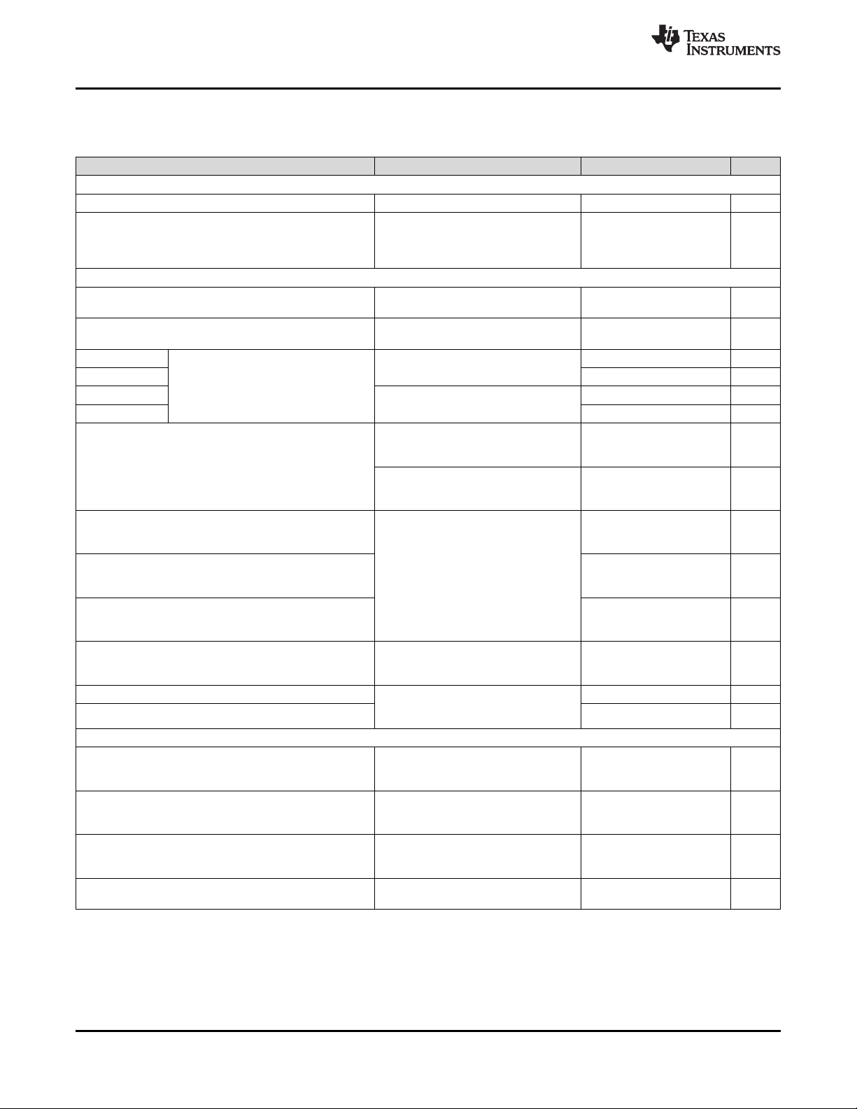
Recovered
³GLUW\´FORFNV
or clean clocks
0XOWLSOH³FOHDQ´
clocks at different
frequencies
CLKout2
CLKout3
CLKout0
FPGA
CLKin0
Crystal or
VCXO
Backup
Reference
Clock
CLKin1
OSCout0
CLKout4
DAC
ADC
LMX2541
PLL+VCO
Serializer/
Deserializer
LMK04906
Precision Clock
Conditioner
CLKout1
CLKin2
CPLD
Copyright © 2016, Texas Instruments Incorporated
Product
Folder
Order
Now
Technical
Documents
Tools &
Software
Support &
Community
SNAS589F –JUNE 2012–REVISED AUGUST 2017
LMK04906 Ultralow Noise Clock Jitter Cleaner and Multiplier With
6 Programmable Outputs
LMK04906
1 Features
1
• Ultralow RMS Jitter Performance
– 100-fs RMS Jitter (12 kHz to 20 MHz)
– 123-fs RMS Jitter (100 Hz to 20 MHz)
• Dual Loop PLLatinum™ PLL Architecture
– PLL1
– Integrated Low-Noise Crystal Oscillator
Circuit
– Holdover Mode when Input Clocks are Lost
– Automatic or Manual
Triggering/Recovery
– PLL2
– Normalized [1 Hz] PLL Noise Floor of –227
dBc/Hz
– Phase Detector Rate up to 155 MHz
– OSCin Frequency-doubler
– Integrated Low-Noise VCO
• 3 Redundant Input Clocks with LOS
– Automatic and Manual Switch-Over Modes
• 50% Duty Cycle Output Divides, 1 to 1045 (Even
and Odd)
• LVPECL, LVDS, or LVCMOS Programmable
Outputs
• Precision Digital Delay, Fixed or Dynamically
Adjustable
• 25-ps Step Analog Delay Control.
• 6 Differential Outputs. Up to 12 Single Ended.
– Up to 5 VCXO/Crystal Buffered Outputs
• Clock Rates of up to 2600 MHz
• 0-Delay Mode
• Three Default Clock Outputs at Power Up
• Multi-mode: Dual PLL, Single PLL, and Clock
Distribution
• Industrial Temperature Range: –40 to 85 °C
• 3.15-V to 3.45-V Operation
• Package: 64-Pin WQFN (9 mm × 9 mm × 0.8 mm)
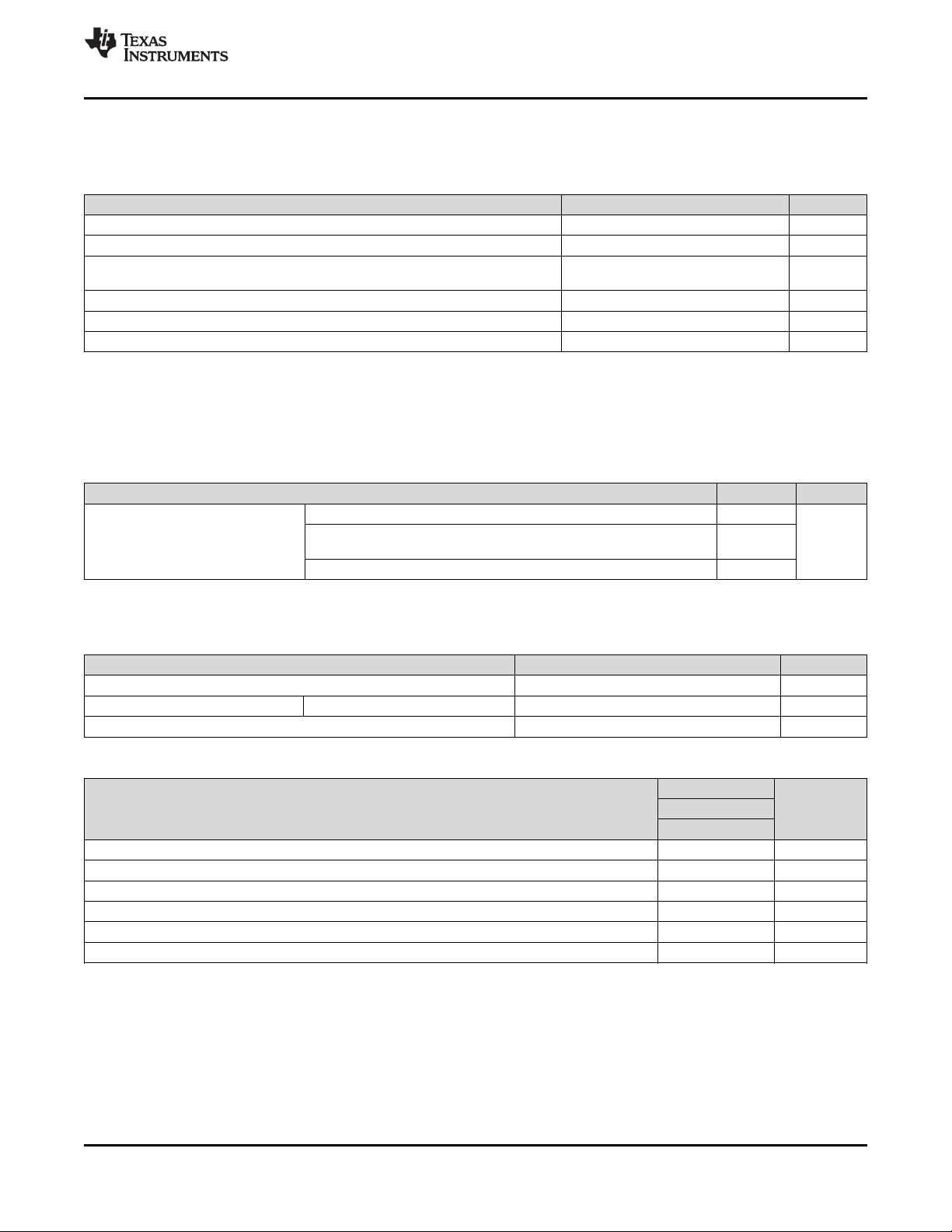
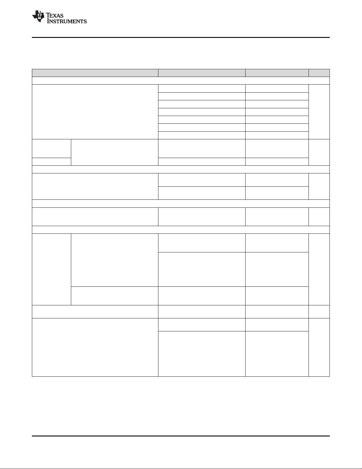
System Application Diagram
2 Applications
• 10G, 40G, and 100G OTN Line Cards
• SONET/SDH OC-48/STM-16 and OC-192/STM64 Line Cards
• GbE/10GbE, 1/2/4/8/10GFC Line Cards
• ITU G.709 and Custom FEC Line Cards
• Synchronous Ethernet
• Optical Modules
• DSLAM/MSANs
• Test and Measurement
• Broadcast Video
• Wireless Basestations
• Data Converter Clocking
• Microwave ODU and IDUs for Wireless Backhaul
3 Description
The LMK04906 is the industry's highest performance
clock jitter attenuator with superior clock jitter
cleaning, generation, and distribution with advanced
features to meet high performance timing application
needs.
The LMK04906 accepts 3 clock inputs ranging from 1
kHz to 500 MHz and generates 6 unique clock output
frequencies ranging from 284 kHz to 2.6 GHz. The
LMK04906 can also buffer a crystal or VCXO to
generate a 7thunique clock frequency.
The device provides virtually all frequency translation
combinations required for SONET, Ethernet, Fibre
Channel and multi-mode Wireless Base Stations.
The LMK04906 input clock frequency and clock
multiplication ratio are programmable through a SPI
interface.
Device Information
PART NUMBER VCO FREQUENCY
LMK04906 2370 to 2600 MHz 3
(1) For all available packages, see the orderable addendum at
the end of the data sheet.
Simplified LMK04906 Block Diagram
(1)
REFERENCE
INPUTS
1
An IMPORTANT NOTICE at the end of this data sheet addresses availability, warranty, changes, use in safety-critical applications,
intellectual property matters and other important disclaimers. PRODUCTION DATA.
LMK04906
SNAS589F –JUNE 2012–REVISED AUGUST 2017
www.ti.com
Table of Contents
1 Features.................................................................. 1
2 Applications ........................................................... 1
3 Description ............................................................. 1
4 Revision History..................................................... 2
5 Pin Configuration and Functions......................... 3
6 Specifications......................................................... 5
6.1 Absolute Maximum Ratings ..................................... 5
6.2 ESD Ratings.............................................................. 5
6.3 Recommended Operating Conditions ...................... 5
6.4 Thermal Information.................................................. 5
6.5 Electrical Characteristics........................................... 6
6.6 Timing Requirements.............................................. 12
6.7 Typical Characteristics............................................ 13
7 Parameter Measurement Information ................ 14
7.1 Charge Pump Current Specification Definitions...... 14
7.2 Differential Voltage Measurement Terminology...... 15
8 Detailed Description............................................ 17
8.1 Overview ................................................................. 17
8.2 Functional Block Diagram....................................... 21
8.3 Feature Description................................................. 21
8.4 Device Functional Modes........................................ 42
8.5 Programming........................................................... 45
8.6 Register Maps......................................................... 48
9 Application and Implementation ........................ 85
9.1 Application Information............................................ 85
9.2 Typical Application ............................................... 101
9.3 System Examples ................................................. 108
9.4 Do's and Don'ts..................................................... 111
10 Power Supply Recommendations ................... 112
10.1 Pin Connection Recommendations..................... 112
10.2 Current Consumption and Power Dissipation
Calculations............................................................ 113
11 Layout................................................................. 115
11.1 Layout Guidelines ............................................... 115
11.2 Layout Example .................................................. 117
12 Device and Documentation Support............... 118
12.1 Device Support.................................................... 118
12.2 Receiving Notification of Documentation
Updates.................................................................. 118
12.3 Community Resource.......................................... 118
12.4 Trademarks......................................................... 118
12.5 Electrostatic Discharge Caution.......................... 118
12.6 Glossary.............................................................. 118
13 Mechanical, Packaging, and Orderable
Information......................................................... 118
4 Revision History
NOTE: Page numbers for previous revisions may differ from page numbers in the current version.
Changes from Revision E (August 2016) to Revision F Page
• Changed From: CLKout3_PD = 0 To: CLKout2_PD = 0 in Table 7..................................................................................... 37
• Changed From: CLKout3_PD = 0 To: CLKout2_PD = 0 in Table 9..................................................................................... 40
Changes from Revision D (May 2013) to Revision E Page
• Changed 750 to 500............................................................................................................................................................... 1
• Changed 2.26 MHz to 284 kHz .............................................................................................................................................. 1
• Added ESD Ratings table, Feature Description section, Device Functional Modes, Application and Implementation
section, Power Supply Recommendations section, Layout section, Device and Documentation Support section, and
Mechanical, Packaging, and Orderable Information section ................................................................................................. 1
• Changed Clock Switch Event With Holdover section........................................................................................................... 26
• Deleted Clock Switch Event without Holdover section......................................................................................................... 26
• Changed 5 cycles to 5.5 cycles............................................................................................................................................ 38
• Changed 5 cycles to 5.5 cycles............................................................................................................................................ 41
• Added (Auto modes only)..................................................................................................................................................... 70
• Changed equation ................................................................................................................................................................ 94
Changes from Revision C (May 2013) to Revision D Page
• Changed layout of National Semiconductor Data Sheet to TI format. ............................................................................... 115
2
Submit Documentation Feedback Copyright © 2012–2017, Texas Instruments Incorporated
Product Folder Links: LMK04906
6364 62 61 60 59 58 57 56 55 54 53
CLKout4
NC
CLKout5*
Status_CLKin0
CLKout4*
NC
Vcc12
CLKout5
NC
NC
Status_CLKin1
Vcc13
DAP
52 51 50 49
CLKout3
Vcc11
CLKout3*
NC
CLKin2*
NC
NC
Vcc3
Vcc4
NC
CLKout2*
CLKout2
GND
FBCLKin/Fin/CLKin1
Status_Holdover
CLKin0
CLKin0*
Vcc5
CLKin2
38
37
39
40
41
42
43
44
45
46
47
48
Vcc7
CPout2
Vcc9
CLKuWire
OSCin*
OSCout0
OSCout0*
Vcc8
LEuWire
DATAuWire
Vcc10
NC
34
33
35
36
CPout1
Status_LD
Vcc6
OSCin
Vcc2
11
12
10
9
8
7
6
5
4
3
2
1
NC
CLKout0*
NC
CLKout0
NC
SYNC/
Status_CLKin2
NC
NC
Vcc1
LDObyp1
LDObyp2
15
16
14
13CLKout1
CLKout1*
NC
1817 19 20 21 22 23 24 25 26 27 28 29 30 31 32
NC
www.ti.com
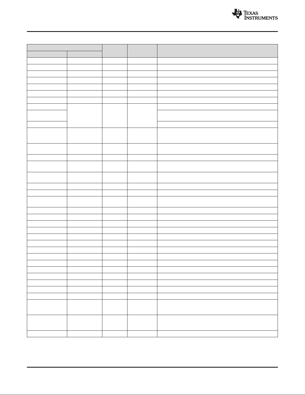
5 Pin Configuration and Functions
LMK04906
SNAS589F –JUNE 2012–REVISED AUGUST 2017
64-Pin WQFN With Exposed Pad
NKD Package
Top View
PIN
2, 5, 7, 8, 9, 15,
22, 47, 51, 55,
17, 19
56, 60,
61, 64
NAME NO.
Vcc13 1 — PWR Power Supply for CLKou0
NC
CLKout0*, CLKout0 3, 4 O Programmable Clock output 0.
SYNC /
Status_CLKin2
Vcc1 10 — PWR Power supply for VCO LDO.
LDObyp1 11 — ANLG LDO Bypass, bypassed to ground with 10 µF capacitor.
(1) See Application and Implementation section for recommended connections.
6 I/O Programmable CLKout Synchronization input or CLKin2 Status output.
I/O TYPE DESCRIPTION
— No Connect These pins must be left floating.
Pin Functions
Submit Documentation FeedbackCopyright © 2012–2017, Texas Instruments Incorporated
Product Folder Links: LMK04906
(1)
3
LMK04906
SNAS589F –JUNE 2012–REVISED AUGUST 2017
www.ti.com
Pin Functions (continued)
PIN
NAME NO.
LDObyp2 12 — ANLG LDO Bypass, bypassed to ground with a 0.1 µF capacitor.
CLKout1, CLKout1* 13, 14 O Programmable Clock output 1.
Vcc2 16 — PWR Power supply for CLKout1.
Vcc3 18 — PWR Power supply for CLKout2
CLKout2*, CLKout2 20, 21 O Programmable Clock output 2
GND 23 — PWR Ground
Vcc4 24 — PWR Power supply for digital.
CLKin1, CLKin1*
FBCLKin, FBCLKin*
Fin/Fin* External VCO input (External VCO mode). AC or DC Coupled.
Status_Holdover 27 I/O Programmable
CLKin0, CLKin0* 28, 29 I ANLG
Vcc5 30 — PWR Power supply for clock inputs.
CLKin2, CLKin2* 31, 32 I ANLG
Status_LD 33 I/O Programmable
CPout1 34 O ANLG Charge pump 1 output.
Vcc6 35 — PWR Power supply for PLL1, charge pump 1.
OSCin, OSCin* 36, 37 I ANLG
Vcc7 38 — PWR Power supply for OSCin port.
OSCout0, OSCout0* 39, 40 O Programmable Buffered output 0 of OSCin port.
Vcc8 41 — PWR Power supply for PLL2, charge pump 2.
CPout2 42 O ANLG Charge pump 2 output.
Vcc9 43 — PWR Power supply for PLL2.
LEuWire 44 I CMOS MICROWIRE Latch Enable Input.
CLKuWire 45 I CMOS MICROWIRE Clock Input.
DATAuWire 46 I CMOS MICROWIRE Data Input.
Vcc10 48 — PWR Power supply for CLKout3.
CLKout3, CLKout3* 49, 50 O Programmable Clock output 3.
Vcc11 52 — PWR Power supply for CLKout4.
CLKout4, CLKout4* 53, 54 O Programmable Clock output 4.
Vcc12 57 — PWR Power supply for CLKout5.
CLKout5, CLKout5* 58, 59 O Programmable Clock output 5.
Status_CLKin0 62 I/O Programmable
Status_CLKin1 63 I/O Programmable
DAP DAP — GND DIE ATTACH PAD, connect to GND.
25, 26 I ANLG
I/O TYPE DESCRIPTION
Reference Clock Input Port 1 for PLL1. AC or DC Coupled.
Feedback input for external clock feedback input (0-delay mode).
AC or DC Coupled.
Programmable status pin, default readback output. Programmable
to holdover mode indicator. Other options available by
programming.
Reference Clock Input Port 0 for PLL1.
AC or DC Coupled.
Reference Clock Input Port 2 for PLL1,
AC or DC Coupled.
Programmable status pin, default lock detect for PLL1 and PLL2.
Other options available by programming.
Feedback to PLL1, Reference input to PLL2.
AC Coupled.
Programmable status pin. Default is input for pin control of PLL1
reference clock selection. CLKin0 LOS status and other options
available by programming.
Programmable status pin. Default is input for pin control of PLL1
reference clock selection. CLKin1 LOS status and other options
available by programming.
(1)
4
Submit Documentation Feedback Copyright © 2012–2017, Texas Instruments Incorporated
Product Folder Links: LMK04906
LMK04906
www.ti.com
SNAS589F –JUNE 2012–REVISED AUGUST 2017
6 Specifications
6.1 Absolute Maximum Ratings
over operating free-air temperature range (unless otherwise noted)
V
CC
V
IN
I
IN
Supply voltage
Input voltage –0.3 (VCC+ 0.3) V
Differential input current (CLKinX/X*,
OSCin/OSCin*, FBCLKin/FBCLKin*, Fin/Fin*)
MSL Moisture sensitivity level 3
T
J
T
stg
Junction temperature 150 °C
Storage temperature –65 150 °C
(1) Stresses beyond those listed under Absolute Maximum Ratings may cause permanent damage to the device. These are stress ratings
only, which do not imply functional operation of the device at these or any other conditions beyond those indicated under Recommended
Operating Conditions. Exposure to absolute-maximum-rated conditions for extended periods may affect device reliability.
(2) If Military/Aerospace specified devices are required, please contact the Texas Instruments Sales Office/Distributors for availability and
specifications.
(3) Never to exceed 3.6 V.
(3)
6.2 ESD Ratings
Human-body model (HBM), per ANSI/ESDA/JEDEC JS-001
V
(ESD)
Electrostatic discharge
(1) JEDEC document JEP155 states that 500-V HBM allows safe manufacturing with a standard ESD control process.
(2) JEDEC document JEP157 states that 250-V CDM allows safe manufacturing with a standard ESD control process.
Charged-device model (CDM), per JEDEC specification JESD22-
(2)
C101
Machine model (MM) ±150
(1)(2)
MIN MAX UNIT
–0.3 3.6 V
±5 mA
VALUE UNIT
(1)
±2000
±750
V
6.3 Recommended Operating Conditions
MIN NOM MAX UNIT
T
J
T
A
V
CC
Junction temperature 125 °C
Ambient temperature VCC= 3.3 V –40 25 85 °C
Supply voltage 3.15 3.3 3.45 V
6.4 Thermal Information
LMK04906
THERMAL METRIC
R
θJA
R
θJC(top)
R
θJB
ψ
JT
ψ
JB
R
θJC(bot)
Junction-to-ambient thermal resistance 25.2 °C/W
Junction-to-case (top) thermal resistance 6.9 °C/W
Junction-to-board thermal resistance 4 °C/W
Junction-to-top characterization parameter 0.1 °C/W
Junction-to-board characterization parameter 4 °C/W
Junction-to-case (bottom) thermal resistance 0.8 °C/W
(1) For more information about traditional and new thermal metrics, see the Semiconductor and IC Package Thermal Metrics application
report.
(1)
UNITNKD (WQFN)
64 PINS
Product Folder Links: LMK04906
Submit Documentation FeedbackCopyright © 2012–2017, Texas Instruments Incorporated
5
LMK04906
SNAS589F –JUNE 2012–REVISED AUGUST 2017
www.ti.com
6.5 Electrical Characteristics
(3.15 V ≤ VCC≤ 3.45 V, -40 °C ≤ TA≤ 85 °C. Typical values represent most likely parametric norms at VCC= 3.3 V, TA= 25
°C, at the Recommended Operating Conditions at the time of product characterization and are not ensured.)
PARAMETER TEST CONDITIONS MIN TYP MAX UNIT
CURRENT CONSUMPTION
I
CC_PD
I
CC_CLKS
CLKin0/0*, CLKin1/1*, and CLKin2/2* INPUT CLOCK SPECIFICATIONS
f
CLKin
SLEW
CLKin
VIDCLKin
VSSCLKin 0.5 3.1 Vpp
VIDCLKin
VSSCLKin 0.5 3.1 Vpp
V
CLKin
V
CLKin0-offset
V
CLKin1-offset
V
CLKin2-offset
V
CLKinX-offset
V
CLKin-VIH
V
CLKin-VIL
FBCLKin/FBCLKin* and Fin/Fin* INPUT SPECIFICATIONS
f
FBCLKin
f
Fin
V
FBCLKin/Fin
SLEW
FBCLKin/Fin
(1) Load conditions for output clocks: LVDS: 100 Ω differential. See Current Consumption and Power Dissipation Calculations for ICCfor
specific part configuration and how to calculate ICCfor a specific design.
(2) CLKin0, CLKin1, and CLKin2 maximum is specified by characterization, production tested at 200 MHz.
(3) Specified by characterization.
(4) See Differential Voltage Measurement Terminology for definition of VIDand VODvoltages.
Power Down Supply Current 1 3 mA
All clock delays disabled,
Supply Current with all clocks enabled
(1)
CLKoutX_DIV = 1045,
CLKoutX_TYPE = 1 (LVDS),
410 470 mA
PLL1 and PLL2 locked.
Clock Input Frequency
(2)
Clock Input Slew Rate
(3)
Clock Input
Differential Input Voltage
(4)
Figure 4
20% to 80% 0.15 0.5 V/ns
AC coupled
CLKinX_BUF_TYPE = 0 (Bipolar)
AC coupled
CLKinX_BUF_TYPE = 1 (MOS)
0.001 500 MHz
0.25 1.55 |V|
0.25 1.55 |V|
AC coupled to CLKinX; CLKinX* AC
Clock Input
Single-ended Input Voltage
(3)
coupled to Ground
CLKinX_BUF_TYPE = 0 (Bipolar)
AC coupled to CLKinX; CLKinX* AC
coupled to Ground
0.25 2.4 Vpp
0.25 2.4 Vpp
CLKinX_BUF_TYPE = 1 (MOS)
DC offset voltage between
CLKin0/CLKin0*
20 mV
CLKin0* - CLKin0
DC offset voltage between
CLKin1/CLKin1*
CLKin1* - CLKin1
Each pin AC coupled
CLKin0_BUF_TYPE = 0 (Bipolar)
0 mV
DC offset voltage between
CLKin2/CLKin2*
20 mV
CLKin2* - CLKin2
DC offset voltage between
CLKinX/CLKinX*
CLKinX* - CLKinX
High input voltage DC coupled to CLKinX; CLKinX* AC
Low input voltage 0 0.4 V
Clock Input Frequency
(3)
Clock Input Frequency
(3)
Single Ended
Clock Input Voltage
(3)
Slew Rate on CLKin
(3)
Each pin AC coupled
CLKinX_BUF_TYPE = 1 (MOS)
coupled to Ground
CLKinX_BUF_TYPE = 1 (MOS)
AC coupled
(CLKinX_BUF_TYPE = 0)
MODE = 2 or 8; FEEDBACK_MUX = 6
AC coupled
(CLKinX_BUF_TYPE = 0)
MODE = 3 or 11
AC coupled;
(CLKinX_BUF_TYPE = 0)
AC coupled; 20% to 80%;
(CLKinX_BUF_TYPE = 0)
55 mV
2 V
CC
0.001 1000 MHz
0.001 3100 MHz
0.25 2 Vpp
0.15 0.5 V/ns
V
6
Submit Documentation Feedback Copyright © 2012–2017, Texas Instruments Incorporated
Product Folder Links: LMK04906
LMK04906
www.ti.com
SNAS589F –JUNE 2012–REVISED AUGUST 2017
Electrical Characteristics (continued)
(3.15 V ≤ VCC≤ 3.45 V, -40 °C ≤ TA≤ 85 °C. Typical values represent most likely parametric norms at VCC= 3.3 V, TA= 25
°C, at the Recommended Operating Conditions at the time of product characterization and are not ensured.)
PARAMETER TEST CONDITIONS MIN TYP MAX UNIT
PLL1 SPECIFICATIONS
f
PD1
I
SOURCE
CPout1
I
SINK
CPout1
I
%MIS
CPout1
I
CPout1VTUNE
I
%TEMP
CPout1
I
TRI
CPout1
PN10kHz
PN1Hz Normalized Phase Noise Contribution
PLL2 REFERENCE INPUT (OSCin) SPECIFICATIONS
f
OSCin
SLEW
OSCin
V
OSCin
VIDOSCin
VSSOSCin 0.4 3.1 Vpp
V
OSCin-offset
f
doubler_max
CRYSTAL OSCILLATOR MODE SPECIFICATIONS
f
XTAL
P
XTAL
C
IN
(5) This parameter is programmable
(6) F
OSCin
(7) See Optional Crystal Oscillator Implementation (OSCin/OSCin*)
PLL1 Phase Detector Frequency 40 MHz
V
= VCC/2, PLL1_CP_GAIN = 0 100
PLL1 Charge
Pump Source Current
(5)
PLL1 Charge
Pump Sink Current
(5)
Charge Pump
Sink / Source Mismatch
Magnitude of Charge Pump Current
Variation vs. Charge Pump Voltage
Charge Pump Current vs. Temperature
Variation
Charge Pump TRI-STATELeakage
Current
PLL 1/f Noise at 10-kHz offset.
Normalized to 1-GHz Output
Frequency
CPout1
V
= VCC/2, PLL1_CP_GAIN = 1 200
CPout1
V
= VCC/2, PLL1_CP_GAIN = 2 400
CPout1
V
= VCC/2, PLL1_CP_GAIN = 3 1600
CPout1
V
CPout1=VCC
V
CPout1=VCC
V
CPout1=VCC
V
CPout1=VCC
V
CPout1
0.5 V < V
TA= 25 °C
/2, PLL1_CP_GAIN = 0 –100
/2, PLL1_CP_GAIN = 1 –200
/2, PLL1_CP_GAIN = 2 –400
/2, PLL1_CP_GAIN = 3 –1600
= VCC/2, T = 25 °C 3% 10
< VCC- 0.5 V
CPout1
4%
4%
0.5 V < V
< VCC- 0.5 V 5 nA
CPout
PLL1_CP_GAIN = 400 µA –117
PLL1_CP_GAIN = 1600 µA –118
PLL1_CP_GAIN = 400 µA –221.5
PLL1_CP_GAIN = 1600 µA –223
PLL2 Reference Input
(6)
PLL2 Reference Clock minimum slew
rate on OSCin
Input Voltage for OSCin or OSCin*
(3)
(3)
Differential voltage swing
Figure 4
20% to 80% 0.15 0.5 V/ns
AC coupled; Single-ended (Unused pin
AC coupled to GND)
AC coupled
0.2 2.4 Vpp
0.2 1.55 |V|
DC offset voltage between
OSCin/OSCin*
Each pin AC coupled 20 mV
OSCinX* - OSCinX
Doubler input frequency
Crystal frequency range
(3)
Crystal power dissipation
(3)
(7)
Input capacitance of LMK04906 OSCin
port
EN_PLL2_REF_2X = 1;
OSCin Duty Cycle 40% to 60%
R
< 40 Ω 6 20.5 MHz
ESR
Vectron VXB1 crystal, 20.48 MHz,
R
< 40 Ω
ESR
XTAL_LVL = 0
100 µW
–40 to +85 °C 6 pF
maximum frequency specified by characterization. Production tested at 200 MHz.
µA
µA
dBc/Hz
dBc/Hz
500 MHz
155 MHz
Product Folder Links: LMK04906
Submit Documentation FeedbackCopyright © 2012–2017, Texas Instruments Incorporated
7
LMK04906
SNAS589F –JUNE 2012–REVISED AUGUST 2017
www.ti.com
Electrical Characteristics (continued)
(3.15 V ≤ VCC≤ 3.45 V, -40 °C ≤ TA≤ 85 °C. Typical values represent most likely parametric norms at VCC= 3.3 V, TA= 25
°C, at the Recommended Operating Conditions at the time of product characterization and are not ensured.)
PARAMETER TEST CONDITIONS MIN TYP MAX UNIT
PLL2 PHASE DETECTOR AND CHARGE PUMP SPECIFICATIONS
f
PD2
I
SOURCE PLL2 charge pump source current
CPout
I
SINK PLL2 charge pump sink current
CPout
I
%MIS Charge pump sink/source mismatch V
CPout2
I
CPout2VTUNE
I
%TEMP
CPout2
I
TRI Charge pump leakage 0.5 V < V
CPout2
PN10kHz
PN1Hz Normalized phase noise contribution
INTERNAL VCO SPECIFICATIONS
f
VCO
K
VCO
|ΔTCL|
(8) A specification in modeling PLL in-band phase noise is the 1/f flicker noise, L
noise has a 10 dB/decade slope. PN10kHz is normalized to a 10 kHz offset and a 1 GHz carrier frequency. PN10kHz = L
kHz) - 20log(Fout / 1 GHz), where L
L(f). To measure L
crystal are important to isolating this noise source from the total phase noise, L(f). L
oscillator performance if a low power or noisy source is used. The total PLL in-band phase noise performance is the sum of L
and L
(9) A specification modeling PLL in-band phase noise. The normalized phase noise contribution of the PLL, L
PLL_flat
PN1HZ=L
bandwidth and f
(10) Maximum Allowable Temperature Drift for Continuous Lock is how far the temperature can drift in either direction from the value it was
at the time that the R30 register was last programmed, and still have the part stay in lock. The action of programming the R30 register,
even to the same value, activates a frequency calibration routine. This implies the part will work over the entire frequency range, but if
the temperature drifts more than the maximum allowable drift for continuous lock, then it will be necessary to reload the R30 register to
ensure it stays in lock. Regardless of what temperature the part was initially programmed at, the temperature can never drift outside the
frequency range of -40 °C to 85 °C without violating specifications.
Phase detector frequency 155 MHz
(5)
(5)
Magnitude of charge pump current vs
charge pump voltage variation
Charge pump current vs temperature
variation
PLL 1/f noise at 10-kHz offset
(8)
. Normalized to
1-GHz output frequency
V
CPout2=VCC
V
CPout2=VCC
V
CPout2=VCC
V
CPout2=VCC
V
CPout2=VCC
V
CPout2=VCC
V
CPout2=VCC
V
CPout2=VCC
CPout2=VCC
0.5 V < V
TA= 25 °C
PLL2_CP_GAIN = 400 µA –118
PLL2_CP_GAIN = 3200 µA –121
PLL2_CP_GAIN = 400 µA –222.5
(9)
/2, PLL2_CP_GAIN = 0 100
/2, PLL2_CP_GAIN = 1 400
/2, PLL2_CP_GAIN = 2 1600
/2, PLL2_CP_GAIN = 3 3200
/2, PLL2_CP_GAIN = 0 –100
/2, PLL2_CP_GAIN = 1 –400
/2, PLL2_CP_GAIN = 2 –1600
/2, PLL2_CP_GAIN = 3 –3200
/2, TA= 25 °C 3% 10%
< VCC- 0.5 V
CPout2
4%
4%
< VCC– 0.5 V 10 nA
CPout2
PLL2_CP_GAIN = 3200 µA –227
VCO tuning range LMK04906 2370 2600 MHz
Fine tuning sensitivity
(The range displayed in the typical
column indicates the lower sensitivity is
typical at the lower end of the tuning
LMK04906 16 to 21 MHz/V
range, and the higher tuning sensitivity
is typical at the higher end of the tuning
range).
Allowable temperature drift for
continuous lock
(10) (3)
(f) it is important to be on the 10 dB/decade slope close to the carrier. A high compare frequency and a clean
PLL_flicker
PLL_flicker
(f) is the single side band phase noise of only the flicker noise's contribution to total noise,
After programming R30 for lock, no
changes to output configuration are
permitted to guarantee continuous lock
(f), which is dominant close to the carrier. Flicker
PLL_flicker
(f) can be masked by the reference
PLL_flicker
125 °C
PLL_flicker
(f).
(f), is defined as:
(f) - 20log(N) - 10log(f
PLL_flat
is the phase detector frequency of the synthesizer. L
PDX
PDX
). L
(f) is the single side band phase noise measured at an offset frequency, f, in a 1 Hz
PLL_flat
(f) contributes to the total noise, L(f).
PLL_flat
PLL_flat
µA
µA
dBc/Hz
dBc/Hz
(10
PLL_flicker
(f)
8
Submit Documentation Feedback Copyright © 2012–2017, Texas Instruments Incorporated
Product Folder Links: LMK04906
LMK04906
www.ti.com
SNAS589F –JUNE 2012–REVISED AUGUST 2017
Electrical Characteristics (continued)
(3.15 V ≤ VCC≤ 3.45 V, -40 °C ≤ TA≤ 85 °C. Typical values represent most likely parametric norms at VCC= 3.3 V, TA= 25
°C, at the Recommended Operating Conditions at the time of product characterization and are not ensured.)
PARAMETER TEST CONDITIONS MIN TYP MAX UNIT
CLKout CLOSED LOOP JITTER SPECIFICATIONS USING A COMMERCIAL QUALITY VCXO
Offset = 1 kHz –122.5
Offset = 10 kHz –132.9
Offset = 100 kHz –135.2
Offset = 800 kHz –143.9
Offset = 10 MHz; LVDS –156
Offset = 10 MHz; LVPECL 1600 mVpp –157.5
L(f)
CLKout
LMK04906
f
= 245.76 MHz
CLKout
SSB phase noise
Measured at clock outputs
Value is average for all output types
(12)
Offset = 10 MHz; LVCMOS –157.1
J
CLKout
LVDS/LVPECL/
LVCMOS
LMK04906
f
CLKout
Integrated RMS jitter
(12)
= 245.76 MHz
BW = 12 kHz to 20 MHz 115
BW = 100 Hz to 20 MHz 123
CLKout CLOSED LOOP JITTER SPECIFICATIONS USING THE INTEGRATED LOW NOISE CRYSTAL OSCILLATOR CIRCUIT
LMK04906
f
= 245.76 MHz
CLKout
Integrated RMS jitter
BW = 12 kHz to 20 MHz
XTAL_LVL = 3
BW = 100 Hz to 20 MHz
XTAL_LVL = 3
DEFAULT POWER ON RESET CLOCK OUTPUT FREQUENCY
Default output clock frequency at
f
CLKout-startup
device power on
(14)
CLKout4, LVDS, LMK04906 90 98 110 MHz
CLOCK SKEW AND DELAY
LVDS-to-LVDS, T = 25 °C,
F
= 800 MHz, RL= 100 Ω
CLK
AC coupled
LVPECL-to-LVPECL,
T = 25 °C,
F
= 800 MHz, RL= 100 Ω
CLK
emitter resistors =
|T
SKEW
Maximum CLKoutX to CLKoutY
(15) (3)
|
240 Ω to GND
AC coupled
MixedT
SKEW
Maximum skew between any two
LVCMOS outputs, same CLKout or
different CLKout
(15) (3)
LVDS or LVPECL to LVCMOS
RL= 50 Ω, CL= 5 pF,
T = 25 °C, F
(15)
= 100 MHz.
CLK
Same device, T = 25 °C,
250 MHz
MODE = 2
PLL1_R_DLY = 0; PLL1_N_DLY = 0
MODE = 2
PLL1_R_DLY = 0; PLL1_N_DLY = 0;
VCO Frequency = 2949.12 MHz
Analog delay select = 0;
td
0-DELAY
CLKin to CLKoutX delay
(15)
Feedback clock digital delay = 11;
Feedback clock half step = 1;
Output clock digital delay = 5;
Output clock half step = 0;
(11)
dBc/Hz
(13)
192
450
30
30
100
750 ps
1850
0
fs rms
ps
ps
(11) VCXO used is a 122.88 MHz Crystek CVHD-950-122.880.
(12) f
= 2457.6 MHz, PLL1 parameters: EN_PLL2_REF_2X = 1, PLL2_R = 2, F
VCO
A 122.88 MHz Crystek CVHD-950–122.880. PLL2 parameters: PLL2_R = 1, F
nF, R2 = 620 Ω, PLL2_C3_LF = 0, PLL2_R3_LF = 0, PLL2_C4_LF = 0, PLL2_R4_LF = 0, CLKoutX_DIV = 10, and
= 1.024 MHz, I
PD1
= 122.88 MHz, I
PD2
= 100 μA, loop bandwidth = 10 Hz.
CP1
= 3200 μA, C1 = 47 pF, C2 = 3.9
CP2
CLKoutX_ADLY_SEL = 0.
(13) Crystal used is a 20.48 MHz Vectron VXB1-1150-20M480 and Skyworks varactor diode, SMV-1249-074LF.
(14) CLKout3 and OSCout0 also oscillate at start-up at the frequency of the VCXO attached to OSCin port.
(15) Equal loading and identical clock output configuration on each clock output is required for specification to be valid. Specification not valid
for delay mode.
Submit Documentation FeedbackCopyright © 2012–2017, Texas Instruments Incorporated
Product Folder Links: LMK04906
9
LMK04906
SNAS589F –JUNE 2012–REVISED AUGUST 2017
www.ti.com
Electrical Characteristics (continued)
(3.15 V ≤ VCC≤ 3.45 V, -40 °C ≤ TA≤ 85 °C. Typical values represent most likely parametric norms at VCC= 3.3 V, TA= 25
°C, at the Recommended Operating Conditions at the time of product characterization and are not ensured.)
PARAMETER TEST CONDITIONS MIN TYP MAX UNIT
LVDS CLOCK OUTPUTS (CLKoutX), CLKoutX_TYPE = 1
f
CLKout
V
OD
V
SS
ΔV
OD
V
OS
ΔV
OS
TR/ T
F
I
SA
I
SB
I
SAB
LVPECL CLOCK OUTPUTS (CLKoutX)
f
CLKout
TR/ T
F
700-mVpp LVPECL CLOCK OUTPUTS (CLKoutX), CLKoutX_TYPE = 2
V
OH
V
OL
V
OD
V
SS
1200-mVpp LVPECL CLOCK OUTPUTS (CLKoutX), CLKoutX_TYPE = 3
V
OH
V
OL
V
OD
V
SS
1600-mVpp LVPECL CLOCK OUTPUTS (CLKoutX), CLKoutX_TYPE = 4
V
OH
V
OL
V
OD
V
SS
(16) See Typical Characteristics for output operation performance at higher frequencies than the minimum maximum output frequency.
Maximum frequency
(3) (16)
Differential output voltage
Figure 5
Change in Magnitude of VODfor
complementary output states
Output offset voltage 1.125 1.25 1.375 V
Change in VOSfor complementary
output states
Output rise time 20% to 80%, RL = 100 Ω
Output fall time 80% to 20%, RL = 100 Ω
Output short-circuit current: single
ended
RL= 100 Ω 1536 MHz
250 400 450 |mV|
500 800 900 mVpp
T = 25 °C, DC measurement
AC coupled to receiver input
–50 50 mV
R = 100 Ω differential termination
35 |mV|
200 ps
Single-ended output shorted to GND, T
= 25 °C
–24 24 mA
Output short-circuit current: differential Complimentary outputs tied together –12 12 mA
Maximum frequency
(3) (16)
1536 MHz
20% to 80% output rise RL = 100 Ω, emitter resistors = 240 Ω
80% to 20% output fall time
Output high voltage
Output low voltage
Output voltage
Figure 5
Output high voltage
Output low voltage
Output voltage
Figure 5
Output high voltage
Output low voltage
Output voltage
Figure 5
to GND
CLKoutX_TYPE = 4 or 5
(1600 or 2000 mVpp)
T = 25 °C, DC measurement
Termination = 50 Ω to
VCC- 1.4 V
T = 25 °C, DC measurement
Termination = 50 Ω to
VCC– 1.7 V
T = 25 °C, DC Measurement
Termination = 50 Ω to
VCC– 2 V
305 380 440 |mV|
610 760 880 mVpp
545 625 705 |mV|
1090 1250 1410 mVpp
660 870 965 |mV|
1320 1740 1930 mVpp
150 ps
VCC–
1.03
VCC–
1.41
VCC–
1.07
VCC–
1.69
VCC–
1.10
VCC–
1.97
V
V
V
V
V
V
10
Submit Documentation Feedback Copyright © 2012–2017, Texas Instruments Incorporated
Product Folder Links: LMK04906
LMK04906
www.ti.com
SNAS589F –JUNE 2012–REVISED AUGUST 2017
Electrical Characteristics (continued)
(3.15 V ≤ VCC≤ 3.45 V, -40 °C ≤ TA≤ 85 °C. Typical values represent most likely parametric norms at VCC= 3.3 V, TA= 25
°C, at the Recommended Operating Conditions at the time of product characterization and are not ensured.)
PARAMETER TEST CONDITIONS MIN TYP MAX UNIT
2000-mVpp LVPECL (2VPECL) CLOCK OUTPUTS (CLKoutX), CLKoutX_TYPE = 5
V
OH
V
OL
V
OD
V
SS
Output high voltage
Output low voltage
Output voltage
Figure 5
T = 25 °C, DC Measurement
Termination = 50 Ω to
VCC– 2.3 V
LVCMOS CLOCK OUTPUTS (CLKoutX)
f
CLKout
V
OH
V
OL
I
OH
I
OL
DUTY
T
R
T
F
CLK
Maximum frequency
(3) (16)
5-pF Load 250 MHz
Output high voltage 1-mA Load
Output low voltage 1-mA Load 0.1 V
Output high current (source) VCC= 3.3 V, VO= 1.65 V 28 mA
Output low current (sink) VCC= 3.3 V, VO= 1.65 V 28 mA
Output duty cycle
(3)
Output rise time
Output fall time
VCC/2 to VCC/2, F
25 °C
20% to 80%, RL = 50 Ω,
CL = 5 pF
80% to 20%, RL = 50 Ω,
CL = 5 pF
DIGITAL OUTPUTS (Status_CLKinX, Status_LD, Status_Holdover, SYNC)
V
OH
V
OL
High-level output voltage IOH= -500 µA
Low-level output voltage IOL= 500 µA 0.4 V
DIGITAL INPUTS (Status_CLKinX, SYNC)
V
IH
V
IL
High-level input voltage 1.6 V
Low-level input voltage 0.4 V
Status_CLKinX_TYPE = 0
(High Impedance)
I
IH
High-level input current
VIH= V
CC
Status_CLKinX_TYPE = 1
(Pull-up)
Status_CLKinX_TYPE = 2
(Pull-down)
Status_CLKinX_TYPE = 0
(High Impedance)
I
IL
Low-level input current
VIL= 0 V
Status_CLKinX_TYPE = 1
(Pull-up)
Status_CLKinX_TYPE = 2
(Pulldown)
DIGITAL INPUTS (CLKuWire, DATAuWire, LEuWire)
V
IH
V
IL
I
IH
I
IL
High-level input voltage 1.6 V
Low-level input voltage 0.4 V
High-level input current VIH= V
CC
Low-level input current VIL= 0 –5 5 µA
= 100 MHz, T =
CLK
1600 2140 2400 mVpp
VCC–
45% 50% 55%
VCC–
VCC–
1.13
VCC–
2.20
800 1070 1200 |mV|
0.1
400 ps
400 ps
0.4
CC
–5 5
–5 5
µA
10 80
–5 5
–40 –5
µA
–5 5
CC
5 25 µA
V
V
V
V
V
V
Product Folder Links: LMK04906
Submit Documentation FeedbackCopyright © 2012–2017, Texas Instruments Incorporated
11
LMK04906
SNAS589F –JUNE 2012–REVISED AUGUST 2017
6.6 Timing Requirements
T
T
T
T
T
T
T
T
ECS
DCS
CDH
CWH
CWL
CES
EWH
CR
LE to Clock Set Up Time See Figure 6 25 ns
Data to Clock Set Up Time See Figure 6 25 ns
Clock to Data Hold Time See Figure 6 8 ns
Clock Pulse Width High See Figure 6 25 ns
Clock Pulse Width Low See Figure 6 25 ns
Clock to LE Set Up Time See Figure 6 25 ns
LE Pulse Width See Figure 6 25 ns
Falling Clock to Readback Time See Figure 9 25 ns
www.ti.com
MIN NOM MAX UNIT
12
Submit Documentation Feedback Copyright © 2012–2017, Texas Instruments Incorporated
Product Folder Links: LMK04906
0 500 1000 1500 2000 2500 3000
0
200
400
600
800
1000
1200
V
OD
(mV)
FREQUENCY (MHz)
2000 mVpp
1600 mVpp
0 500 1000 1500 2000 2500 3000
0
50
100
150
200
250
300
350
400
450
500
V
OD
(mV)
FREQUENCY (MHz)
0 500 1000 1500 2000 2500 3000
0
200
400
600
800
1000
1200
V
OD
(mV)
FREQUENCY (MHz)
2000 mVpp
1600 mVpp
1200 mVpp
700 mVpp
www.ti.com
6.7 Typical Characteristics
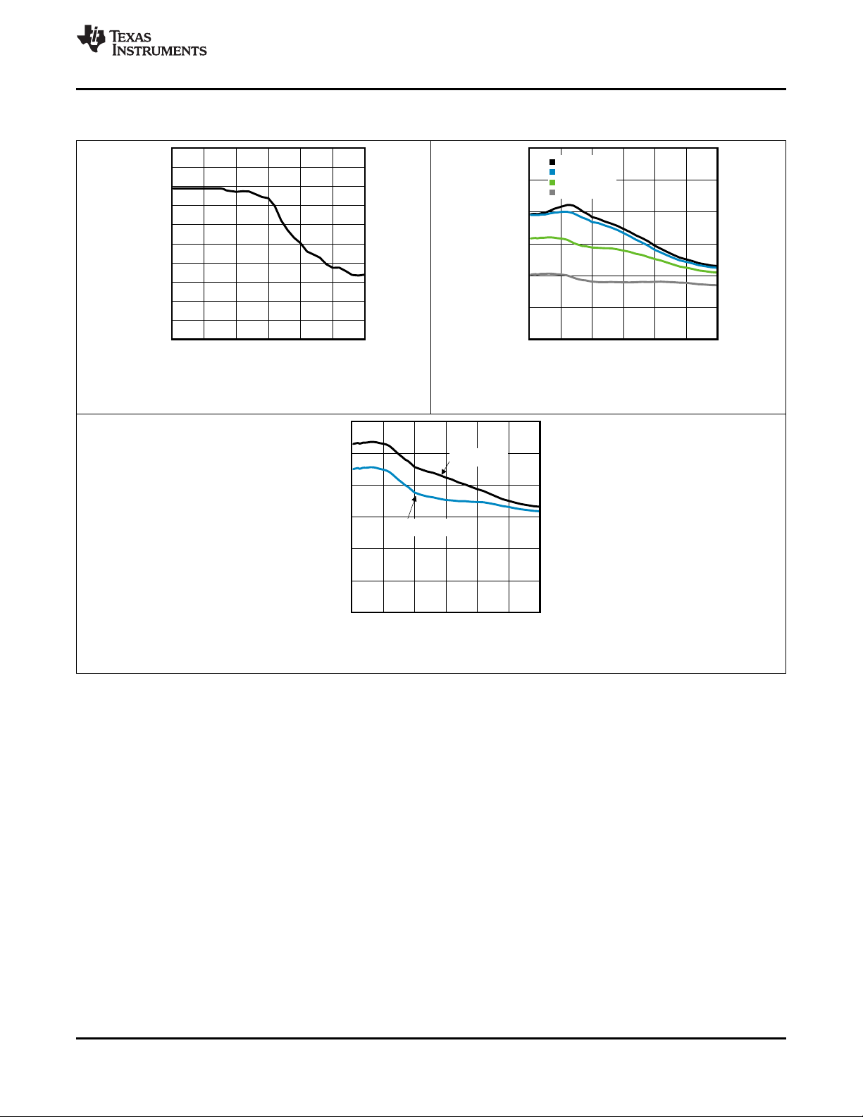
Figure 1. LVDS VODvs Frequency Figure 2. LVPECL With 240-Ω Emitter Resistors VODvs
LMK04906
SNAS589F –JUNE 2012–REVISED AUGUST 2017
Frequency
Figure 3. LVPECL With 120-Ω Emitter Resistors VODvs Frequency
Submit Documentation FeedbackCopyright © 2012–2017, Texas Instruments Incorporated
Product Folder Links: LMK04906
13
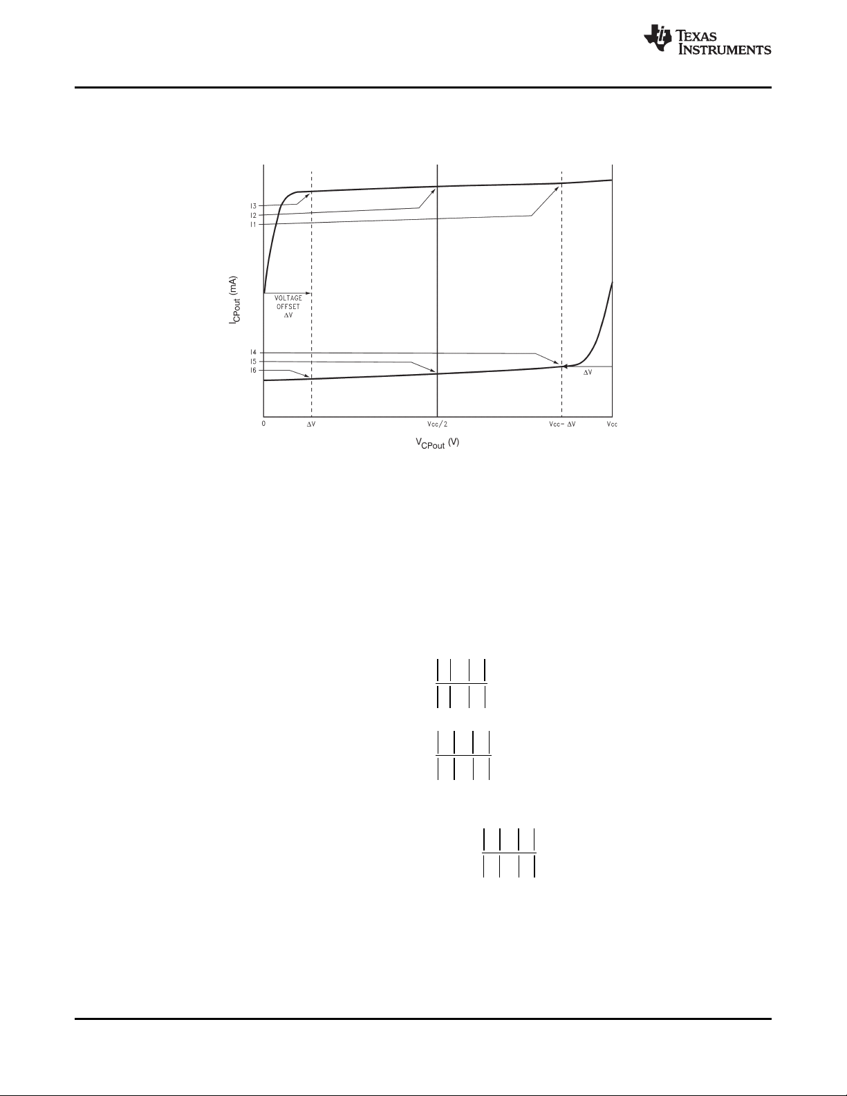
CPout CPout
I2 I5
I2 I5
-
= ´
+
CPout CPout
I1 I3
I1 I3
-
= ´
+
I4 I6
100%
I4 I6
-
= ´
+
LMK04906
SNAS589F –JUNE 2012–REVISED AUGUST 2017
7 Parameter Measurement Information
7.1 Charge Pump Current Specification Definitions
www.ti.com
I1 = Charge Pump Sink Current at V
I2 = Charge Pump Sink Current at V
I3 = Charge Pump Sink Current at V
I4 = Charge Pump Source Current at V
I5 = Charge Pump Source Current at V
I6 = Charge Pump Source Current at V
ΔV = Voltage offset from the positive and negative supply rails. Defined to be 0.5 V for this device.
7.1.1 Charge Pump Output Current Magnitude Variation Vs. Charge Pump Output Voltage
7.1.2 Charge Pump Sink Current Vs. Charge Pump Output Source Current Mismatch
CPout
CPout
CPout
CPout
CPout
CPout
= VCC- ΔV
= VCC/2
= ΔV
= VCC- ΔV
= VCC/2
= ΔV
14
Submit Documentation Feedback Copyright © 2012–2017, Texas Instruments Incorporated
Product Folder Links: LMK04906
V
A
V
B
GND
VID = | VA - VB |
VSS = 2·V
ID
VID Definition VSS Definition for Input
Non-Inverting Clock
Inverting Clock
V
ID
2·V
ID
A
A
A
2 T 2
T 25 C
CPout A
2 T 25 C
I I
I
= °
= °
-
= ´
A
A
A
5 T 5
T 25 C
5 T 25 C
I I
100%
I
= °
= °
-
= ´
LMK04906
www.ti.com
SNAS589F –JUNE 2012–REVISED AUGUST 2017
Charge Pump Current Specification Definitions (continued)
7.1.3 Charge Pump Output Current Magnitude Variation vs Temperature
7.2 Differential Voltage Measurement Terminology
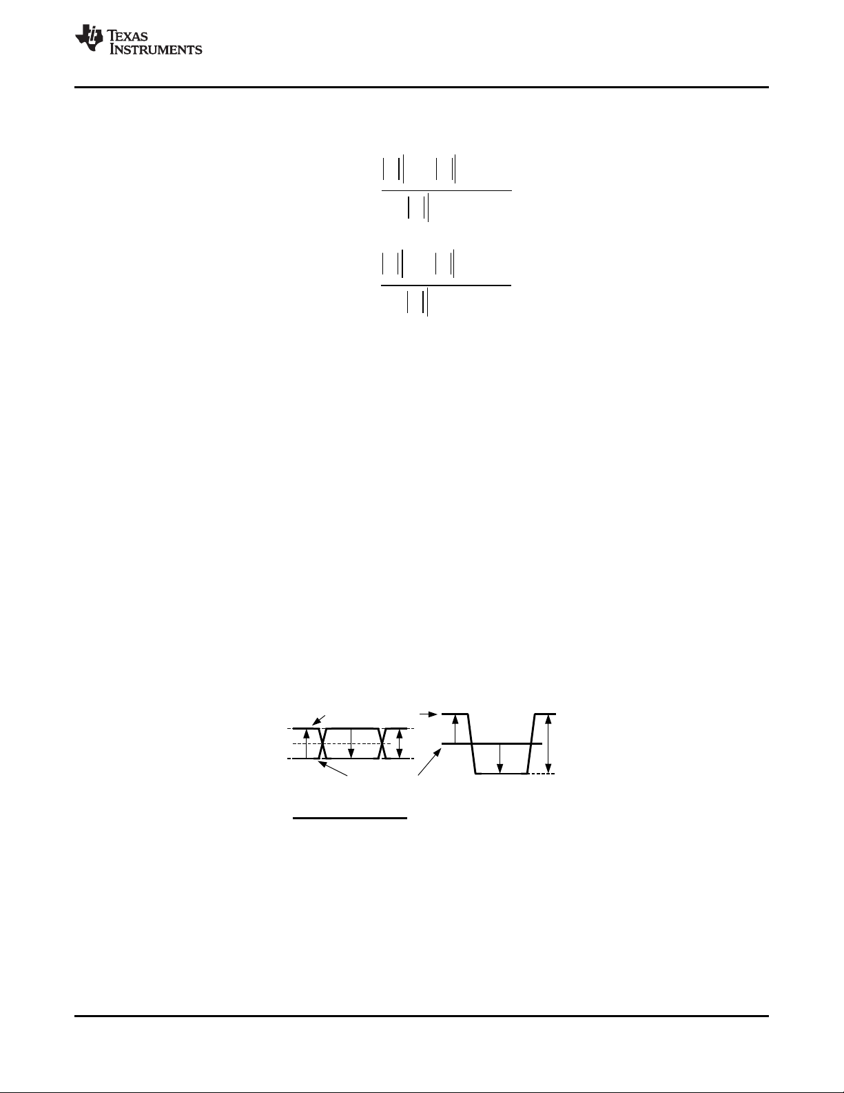
The differential voltage of a differential signal can be described by two different definitions causing confusion
when reading datasheets or communicating with other engineers. This section will address the measurement and
description of a differential signal so that the reader will be able to understand and discern between the two
different definitions when used.
The first definition used to describe a differential signal is the absolute value of the voltage potential between the
inverting and non-inverting signal. The symbol for this first measurement is typically VIDor VODdepending on if
an input or output voltage is being described.
The second definition used to describe a differential signal is to measure the potential of the non-inverting signal
with respect to the inverting signal. The symbol for this second measurement is VSSand is a calculated
parameter. Nowhere in the IC does this signal exist with respect to ground, it only exists in reference to its
differential pair. VSScan be measured directly by oscilloscopes with floating references, otherwise this value can
be calculated as twice the value of VODas described in the first description.
Figure 4 illustrates the two different definitions side-by-side for inputs and Figure 5 illustrates the two different
definitions side-by-side for outputs. The VIDand VODdefinitions show VAand VBDC levels that the non-inverting
and inverting signals toggle between with respect to ground. VSSinput and output definitions show that if the
inverting signal is considered the voltage potential reference, the non-inverting signal voltage potential is now
increasing and decreasing above and below the non-inverting reference. Thus the peak-to-peak voltage of the
differential signal can be measured.
VIDand VODare often defined as volts (V) and VSSis often defined as volts peak-to-peak (VPP).
Figure 4. Two Different Definitions for Differential Input Signals
Product Folder Links: LMK04906
Submit Documentation FeedbackCopyright © 2012–2017, Texas Instruments Incorporated
15
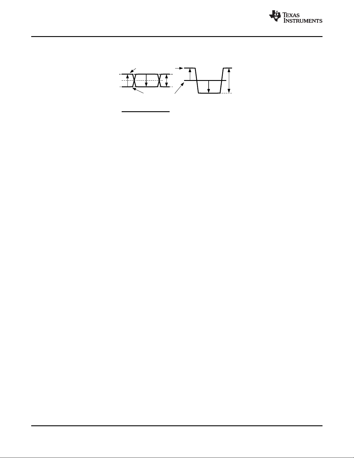
V
A
V
B
GND
VOD = | VA - VB |
VSS = 2·V
OD
VOD Definition VSS Definition for Output
Non-Inverting Clock
Inverting Clock
V
OD
2·V
OD
LMK04906
SNAS589F –JUNE 2012–REVISED AUGUST 2017
Differential Voltage Measurement Terminology (continued)
See the AN-912 Common Data Transmission Parameters and Their Definitions (SNLA036) application note for more
information.
Figure 5. Two Different Definitions for Differential Output Signals
www.ti.com
16
Submit Documentation Feedback Copyright © 2012–2017, Texas Instruments Incorporated
Product Folder Links: LMK04906

LMK04906
www.ti.com
SNAS589F –JUNE 2012–REVISED AUGUST 2017
8 Detailed Description
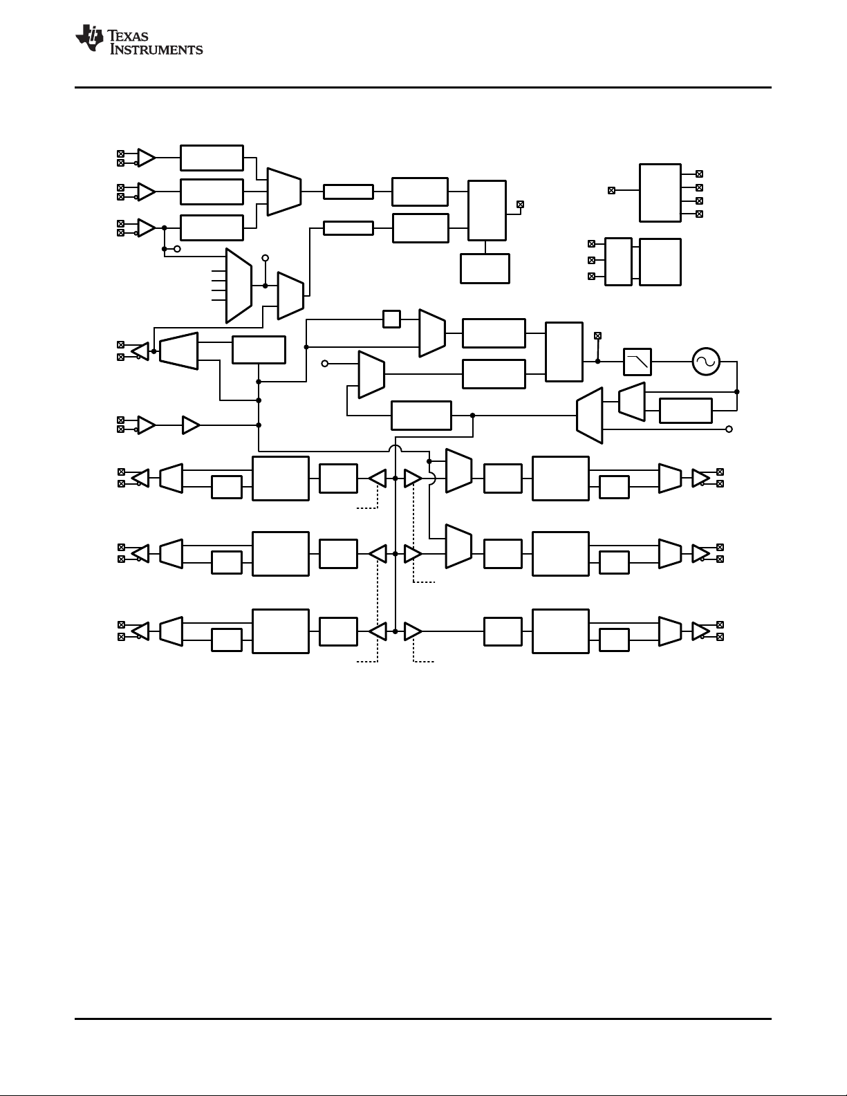
8.1 Overview
In default mode of operation, dual PLL mode with internal VCO, the Phase Frequency Detector in PLL1
compares the active CLKinX reference divided by CLKinX_PreR_DIV and PLL1 R divider with the external
VCXO or crystal attached to the PLL2 OSCin port divided by PLL1 N divider. The external loop filter for PLL1
should be narrow to provide an ultra clean reference clock from the external VCXO or crystal to the
OSCin/OSCin* pins for PLL2.
The Phase Frequency Detector in PLL2 compares the external VCXO or crystal attached to the OCSin port
divided by the PLL2 R divider with the output of the internal VCO divided by the PLL2 N divider and N2 prescaler and optionally the VCO divider. The bandwidth of the external loop filter for PLL2 should be designed to
be wide enough to take advantage of the low in-band phase noise of PLL2 and the low high offset phase noise of
the internal VCO. The VCO output is also placed on the distribution path for the clock distribution section. The
clock distribution consists of 6 dividers and delays which drive 6 outputs. Each clock output allows the user to
select a divide value, a digital delay value, and an analog delay. The 6 dividers drive programmable output
buffers. Two outputs allow their input signal to be from the OSCin port directly.
When a 0-delay mode is used, a clock output will be passed through the feedback mux to the PLL1 N Divider for
synchronization and 0-delay.
When an external VCO mode is used, the Fin port will be used to input an external VCO signal. PLL2 Phase
comparison will now be with this signal divided by the PLL2 N divider and N2 pre-scaler. The VCO divider may
not be used. One less clock input is available when using an external VCO mode.
When a single PLL mode is used, PLL1 is powered down. OSCin is used as a reference to PLL2.
8.1.1 System Architecture
The dual loop PLL architecture of the LMK04906 provides the lowest jitter performance over the widest range of
output frequencies and phase noise integration bandwidths. The first stage PLL (PLL1) is driven by an external
reference clock and uses an external VCXO or tunable crystal to provide a frequency accurate, low phase noise
reference clock for the second stage frequency multiplication PLL (PLL2). PLL1 typically uses a narrow loop
bandwidth (10 Hz to 200 Hz) to retain the frequency accuracy of the reference clock input signal while at the
same time suppressing the higher offset frequency phase noise that the reference clock may have accumulated
along its path or from other circuits. This “cleaned” reference clock provides the reference input to PLL2.
The low phase noise reference provided to PLL2 allows PLL2 to operate with a wide loop bandwidth (50 kHz to
200 kHz). The loop bandwidth for PLL2 is chosen to take advantage of the superior high offset frequency phase
noise profile of the internal VCO and the good low offset frequency phase noise of the reference VCXO or
tunable crystal.
Ultra low jitter is achieved by allowing the external VCXO or Crystal’s phase noise to dominate the final output
phase noise at low offset frequencies and the internal VCO’s phase noise to dominate the final output phase
noise at high offset frequencies. This results in best overall phase noise and jitter performance.
The LMK04906 allows subsets of the device to be used to increase the flexibility of device. These different
modes are selected using MODE: Device Mode. For instance:
• Dual Loop Mode - Typical use case of LMK04906. CLKinX used as reference input to PLL1, OSCin port is
connected to VCXO or tunable crystal.
• Single Loop Mode - Powers down PLL1. OSCin port is used as reference input.
• Clock Distribution Mode - Allows input of CLKin1 to be distributed to output with division, digital delay, and
analog delay.
See Device Functional Modes for more information on these modes.
8.1.2 PLL1 Redundant Reference Inputs (CLKin0/CLKin0*, CLKin1/CLKin1*, and CLKin2/CLKin2*)
The LMK04906 has three reference clock inputs for PLL1, CLKin0, CLKin1, and CLKin2. Ref Mux selects
CLKin0, CLKin1, or CLKin2. Automatic or manual switching occurs between the inputs.
Submit Documentation FeedbackCopyright © 2012–2017, Texas Instruments Incorporated
Product Folder Links: LMK04906
17

LMK04906
SNAS589F –JUNE 2012–REVISED AUGUST 2017
www.ti.com
Overview (continued)
CLKin0, CLKin1, and CLKin2 each have input dividers. The input divider allows different clock input frequencies
to be normalized so that the frequency input to the PLL1 R divider remains constant during automatic switching.
By programming these dividers such that the frequency presented to the input of the PLL1_R divider is the same
prevents the user from needing to reprogram the PLL1 R divider when the input reference is changed to another
CLKin port with a different frequency.
CLKin1 is shared for use as an external 0-delay feedback (FBCLKin), or for use with an external VCO (Fin).
Fast manual switching between reference clocks is possible with a external pins Status_CLKin0, Status_CLKin1,
Status_CLKin2. If Status_CLKinx pins are used to select the reference clock, a minimum pulse width of 500ns
must be met.
8.1.3 PLL1 Tunable Crystal Support
The LMK04906 integrates a crystal oscillator on PLL1 for use with an external crystal and varactor diode to
perform jitter cleaning.
The LMK04906 must be programmed to enable Crystal mode.
8.1.4 VCXO/Crystal Buffered Outputs
The LMK04906 provides a dedicated output which is a buffered copy of the PLL2 reference input. This reference
input is typically a low noise VCXO or Crystal. When using a VCXO, this output can be used to clock external
devices such as microcontrollers, FPGAs, CPLDs, etc. before the LMK04906 is programmed.
The OSCout0 buffer output type is programmable to LVDS, LVPECL, or LVCMOS.
The dedicated output buffer OSCout0 can output frequency lower than the VCXO or Crystal frequency by
programming the OSC Divider. The OSC Divider value range is 1 to 8. Each OSCoutX can individually choose to
use the OSC Divider output or to bypass the OSC Divider.
Two clock outputs can also be programmed to be driven by OSCin. This allows a total of 2 additional differential
outputs to be buffered outputs of OSCin. When programmed in this way, a total of 3 differential outputs can be
driven by a buffered copy of OSCin.
VCXO/Crystal buffered outputs cannot be synchronized to the VCO clock distribution outputs. The assertion of
SYNC will still cause these outputs to become low. Since these outputs will turn off and on asynchronously with
respect to the VCO sourced clock outputs during a SYNC, it is possible for glitches to occur on the buffered clock
outputs when SYNC is asserted and unasserted. If the NO_SYNC_CLKoutX bits are set these outputs will not be
affected by the SYNC event except that the phase relationship will change with the other synchronized clocks
unless a buffered clock output is used as a qualification clock during SYNC.
8.1.5 Frequency Holdover
The LMK04906 supports holdover operation to keep the clock outputs on frequency with minimum drift when the
reference is lost until a valid reference clock signal is re-established.
8.1.6 Integrated Loop Filter Poles
The LMK04906 features programmable 3rd and 4th order loop filter poles for PLL2. These internal resistors and
capacitor values may be selected from a fixed range of values to achieve either a 3rd or 4th order loop filter
response. The integrated programmable resistors and capacitors compliment external components mounted near
the chip.
These integrated components can be effectively disabled by programming the integrated resistors and capacitors
to their minimum values.
8.1.7 Internal VCO
The output of the internal VCO is routed to a mux which allows the user to select either the direct VCO output or
a divided version of the VCO for the Clock Distribution Path. This same selection is also fed back to the PLL2
phase detector through a prescaler and N-divider.
18
Submit Documentation Feedback Copyright © 2012–2017, Texas Instruments Incorporated
Product Folder Links: LMK04906

LMK04906
www.ti.com
SNAS589F –JUNE 2012–REVISED AUGUST 2017
Overview (continued)
The mux selectable VCO divider has a divide range of 2 to 8 with 50% output duty cycle for both even and odd
divide values.
The primary use of the VCO divider is to achieve divides greater than the clock output divider supports alone.
8.1.8 External VCO Mode
The Fin/Fin* input allows an external VCO to be used with PLL2 of the LMK04906.
Using an external VCO reduces the number of available clock inputs by one.
8.1.9 Clock Distribution
The LMK04906 features a total of 6 outputs driven from the internal or external VCO.
All VCO driven outputs have programmable output types. They can be programmed to LVPECL, LVDS, or
LVCMOS. When all distribution outputs are configured for LVCMOS or single ended LVPECL a total of 24
outputs are available.
If the buffered OSCin output OSCout0 is included in the total number of clock outputs the LMK04906 is able to
distribute, then up to 6 differential clocks or up to 12 single ended clocks may be generated with the LMK04906.
The following sections discuss specific features of the clock distribution channels that allow the user to control
various aspects of the output clocks.
8.1.9.1 CLKout DIVIDER
Each clock output has a single clock output divider. The divider supports a divide range of 1 to 1045 (even and
odd) with 50% output duty cycle. When divides of 26 or greater are used, the divider/delay block uses extended
mode.
The VCO Divider may be used to reduce the divide needed by the clock output divider so that it may operate in
normal mode instead of extended mode. This can result in a small current saving if enabling the VCO Divider
allows 3 or more clock output divides to change from extended to normal mode.
8.1.9.2 CLKout Delay
The clock distribution section includes both a fine (analog) and coarse (digital) delay for phase adjustment of the
clock outputs.
The fine (analog) delay allows a nominal 25 ps step size and range from 0 to 475 ps of total delay. Enabling the
analog delay adds a nominal 500 ps of delay in addition to the programmed value. When adjusting analog delay,
glitches may occur on the clock outputs being adjusted. Analog delay may not operate at frequencies above the
minimum-specified maximum output frequency of 1536 MHz.
The coarse (digital) delay allows a group of outputs to be delayed by 4.5 to 12 clock distribution path cycles in
normal mode, or from 12.5 to 522 VCO cycles in extended mode. The delay step can be as small as half the
period of the clock distribution path by using the CLKoutX_HS bit provided the output divide value is greater than
1. For example 2 GHz VCO frequency without using the VCO divider results in 250 ps coarse tuning steps. The
coarse (digital) delay value takes effect on the clock outputs after a SYNC event.
There are 3 different ways to use the digital (coarse) delay.
1. Fixed Digital Delay
2. Absolute Dynamic Digital Delay
3. Relative Dynamic Digital Delay
8.1.9.3 Programmable Output Type
For increased flexibility all LMK04906 clock outputs (CLKoutX) and OSCout0 can be programmed to an LVDS,
LVPECL, or LVCMOS output type.
Any LVPECL output type can be programmed to 700, 1200, 1600, or 2000 mVpp amplitude levels. The 2000
mVpp LVPECL output type is a Texas Instruments proprietary configuration that produces a 2000 mVpp
differential swing for compatibility with many data converters and is also known as 2VPECL.
Submit Documentation FeedbackCopyright © 2012–2017, Texas Instruments Incorporated
Product Folder Links: LMK04906
19

LMK04906
SNAS589F –JUNE 2012–REVISED AUGUST 2017
www.ti.com
Overview (continued)
8.1.9.4 Clock Output Synchronization
Using the SYNC input causes all active clock outputs to share a rising edge. See Clock Output Synchronization
(SYNC) for more information.
The SYNC event also causes the digital delay values to take effect.
8.1.10 0-Delay
The 0-delay mode synchronizes the input clock phase to the output clock phase. The 0-delay feedback may
performed with an internal feedback loop from some of the clock outputs or with an external feedback loop into
the FBCLKin port as selected by the FEEDBACK_MUX.
Without using 0-delay mode there will be n possible fixed phase relationships from clock input to clock output
depending on the clock output divide value.
Using an external 0-delay feedback reduces the number of available clock inputs by one.
8.1.11 Default Start-Up Clocks
Before the LMK04906 is programmed, CLKout4 is enabled and operating at a nominal frequency and CLKout3
and OSCout0 are enabled and operating at the OSCin frequency. These clocks can be used to clock external
devices such as microcontrollers, FPGAs, CPLDs, etc. before the LMK04906 is programmed.
For CLKout3 and OSCout0 to work before the LMK04906 is programmed the device must not be using Crystal
mode.
8.1.12 Status Pins
The LMK04906 provides status pins which can be monitored for feedback or in some cases used for input
depending upon device programming. For example:
• The Status_Holdover pin may indicate if the device is in hold-over mode.
• The Status_CLKin0 pin may indicate the LOS (loss-of-signal) for CLKin0.
• The Status_CLKin0 pin may be an input for selecting the active clock input.
• The Status_LD pin may indicate if the device is locked.
The status pins can be programmed to a variety of other outputs including analog lock detect, PLL divider
outputs, combined PLL lock detect signals, PLL1 Vtune railing, readback, and so forth. See Status PINS of this
data sheet for more information. Default pin programming is captured in Table 17.
8.1.13 Register Readback
Programmed registers may be read back using the MICROWIRE interface. For readback one of the status pins
must be programmed for readback mode.
At no time may registers be programed to values other than the valid states defined in the data sheet.
20
Submit Documentation Feedback Copyright © 2012–2017, Texas Instruments Incorporated
Product Folder Links: LMK04906
CLKuWire
DATAuWire
LEuWire
R1 Divider
(1 to 16,383)
CPout1
Internal VCO
Partially
Integrated
Loop Filter
2X
Mux
R Delay
N Delay
OSCin*
OSCin
FB
Mux
2X
Control
Registers
PWire
Port
SYNC/
Status_CLKin2
Status_LD
Status_Holdover
Status_CLKin0
Device
Control
Status_CLKin1
Holdover
CLKin0*
CLKin0
Divider
(1 to 1045)
Digital
Delay
CLKout1
CLKout3
CLKout4
CLKout5
VCO Divider
(2 to 8)
Osc
Mux1
Osc
Mux2
CPout2
CLKin0 Divider
(1, 2, 4, or 8)
N1 Divider
(1 to 16,383)
R2 Divider
(1 to 4,095)
Phase
Detector
PLL1
Phase
Detector
PLL2
N2 Divider
(1 to 262,143)
Delay
Clock Buffer 2
Clock Buffer 1
Clock Buffer 1
Clock Buffer 3
Clock Distribution PathN2 Prescaler
(2 to 8)
VCO
Mux
Fin/Fin*
Fin/Fin*
CLKin1 Divider
(1, 2, 4, or 8)
OSCout0
OSCout0*
OSCout0
_MUX
OSC Divider
(2 to 8)
CLKin1*/Fin*
FBCLKin*
CLKin1/
Fin/FBCLKin
Mode
Mux2
Mode
Mux1
OSCout0
_MUX
Mode
Mux3
FBMux
FBMux
CLKin2*
CLKin2
CLKin2 Divider
(1, 2, 4, or 8)
Ref
Mux
CLKout0
CLKout0*
Mux
Divider
(1 to 1045)
Digital
Delay
Delay
CLKout1
CLKout1*
Mux
Divider
(1 to 1045)
Digital
Delay
Delay
CLKout2
CLKout2*
Mux
Divider
(1 to 1045)
Digital
Delay
Delay
CLKout4
CLKout4*
Mux
Divider
(1 to 1045)
Digital
Delay
Delay
CLKout5
CLKout5*
Mux
Divider
(1 to 1045)
Digital
Delay
Delay
CLKout3
CLKout3*
Mux
Copyright © 2016, Texas Instruments Incorporated
www.ti.com
8.2 Functional Block Diagram
LMK04906
SNAS589F –JUNE 2012–REVISED AUGUST 2017
8.3 Feature Description
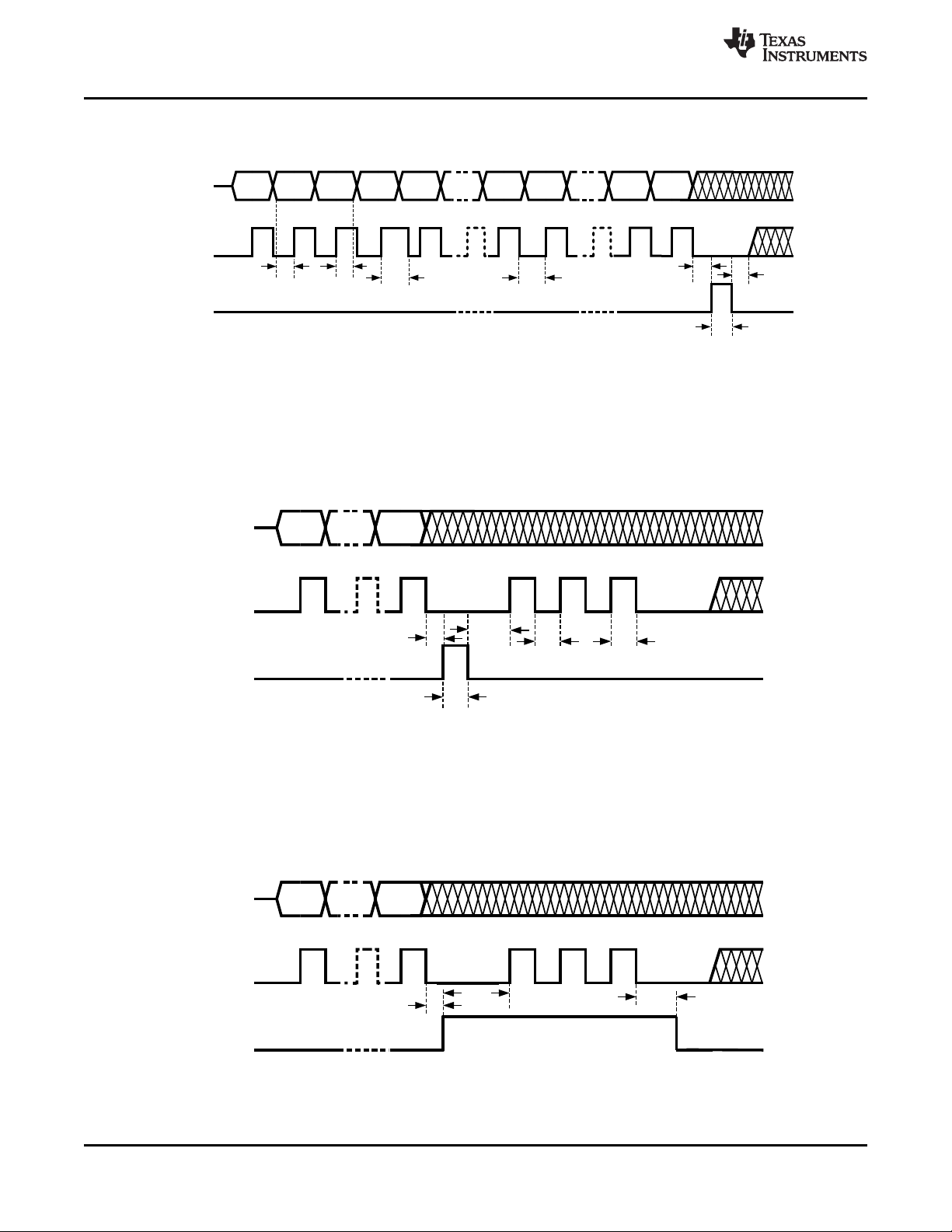
8.3.1 Serial MICROWIRE Timing Diagram
Register programming information on the DATAuWire pin is clocked into a shift register on each rising edge of
the CLKuWire signal. On the rising edge of the LEuWire signal, the register is sent from the shift register to the
register addressed. A slew rate of at least 30 V/µs is recommended for these signals. After programming is
complete the CLKuWire, DATAuWire, and LEuWire signals should be returned to a low state. If the CLKuWire or
DATAuWire lines are toggled while the VCO is in lock, as is sometimes the case when these lines are shared
with other parts, the phase noise may be degraded during this programming. See Figure 6 for timing diagram.
Product Folder Links: LMK04906
Submit Documentation FeedbackCopyright © 2012–2017, Texas Instruments Incorporated
21
D26 A0
MSB LSB
CLKuWire
LEuWire
t
CES
t
CES
t
ECS
D26 A0
MSB LSB
CLKuWire
LEuWire
t
ECS
t
EWH
t
CWH
t
CWL
t
CES
t
DCS
D26 D25 D24 D23
t
CDH
t
CWH
t
CWL
D22 D0 A4 A1 A0
MSB LSB
CLKuWire
LEuWire
t
CES
t
EWH
t
ECS
LMK04906
SNAS589F –JUNE 2012–REVISED AUGUST 2017
www.ti.com
Feature Description (continued)
Figure 6. MICROWIRE Timing Diagram
8.3.2 Advanced MICROWIRE Timing Diagrams
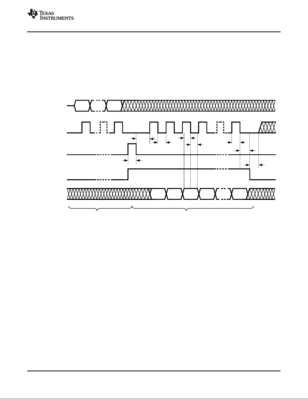
8.3.2.1 Three Extra Clocks or Double Program
Figure 7 shows the timing for the programming sequence for loading CLKoutX_DIV > 25 or CLKoutX_DDLY > 12
as described in Special Programming Case for R0 to R5 for CLKoutX_DIV and CLKoutX_DDLY.
Figure 7. MICROWIRE Timing Diagram: Extra CLKuWire Pulses for R0 to R5
8.3.2.2 Three Extra Clocks With LEuWire High
Figure 8 shows the timing for the programming sequence which allows SYNC_EN_AUTO = 1 when loading
CLKoutX_DIV > 25 or CLKoutX_DDLY > 12. When SYNC_EN_AUTO = 1, a SYNC event is automatically
generated on the falling edge of LEuWire. See Special Programming Case for R0 to R5 for CLKoutX_DIV and
CLKoutX_DDLY.
Figure 8. MICROWIRE Timing Diagram: Extra CLKuWire Pulses for R0 to R5 With LEuWire Asserted
22
Submit Documentation Feedback Copyright © 2012–2017, Texas Instruments Incorporated
Product Folder Links: LMK04906
D26 A0
MSB LSB
DATAuWire
CLKuWire
LEuWire
t
ECS
t
EWH
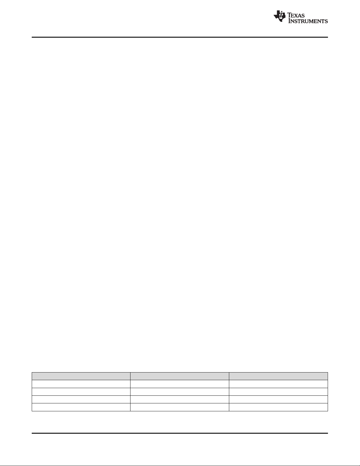
Readback Pin RD0RD24RD26
LEuWire
t
CWH
t
CWL
RD25
t
CR
RD23
t
CR
t
ECS
Register Write Register Read
t
CES
LMK04906
www.ti.com
SNAS589F –JUNE 2012–REVISED AUGUST 2017
Feature Description (continued)
8.3.2.3 Readback
For timing specifications, see Timing Requirements. See Readback for more information on performing a
readback operation. Figure 9 shows timing for LEuWire for both READBACK_LE = 1 and 0.
The rising edges of CLKuWire during MICROWIRE readback continue to clock data on DATAuWire into the
device during readback. If after the readback, LEuWire transitions from low to high, this data will be latched to
the decoded register. The decoded register address consists of the last 5 bits clocked on DATAuWire as shown
in the MICROWIRE Timing Diagrams.
Figure 9. MICROWIRE Readback Timing Diagram
8.3.3 Inputs / Outputs
8.3.3.1 PLL1 Reference Inputs (CLKin0, CLKin1, and CLKin2)
The reference clock inputs for PLL1 may be selected from either CLKin0, CLKin1, or CLKin2. The user has the
capability to manually select one of the inputs or to configure an automatic switching mode of operation. See
Input Clock Switching for more info.
CLKin0, CLKin1, and CLKin2 have dividers which allow the device to switch between reference inputs of different
frequencies automatically without needing to reprogram the PLL1 R divider. The CLKin pre-divider values are 1,
2, 4, and 8.
CLKin1 input can alternatively be used for external feedback in 0-delay mode (FBCLKin) or for an external VCO
input port (Fin).
8.3.3.2 PLL2 OSCin / OSCin* Port
The feedback from the external oscillator being locked with PLL1 drives the OSCin/OSCin* pins. Internally this
signal is routed to the PLL1 N Divider and to the reference input for PLL2.
This input may be driven with either a single-ended or differential signal and must be AC coupled. If operated in
single ended mode, the unused input must be connected to GND with a 0.1-µF capacitor.
Product Folder Links: LMK04906
Submit Documentation FeedbackCopyright © 2012–2017, Texas Instruments Incorporated
23
LMK04906
SNAS589F –JUNE 2012–REVISED AUGUST 2017
www.ti.com
Feature Description (continued)
8.3.3.3 Crystal Oscillator
The internal circuitry of the OSCin port also supports the optional implementation of a crystal based oscillator
circuit. A crystal, a varactor diode, and a small number of other external components may be used to implement
the oscillator. The internal oscillator circuit is enabled by setting the EN_PLL2_XTAL bit. See EN_PLL2_XTAL.
8.3.4 Input Clock Switching
Manual, pin select, and automatic are three different kinds clock input switching modes can be set with the
CLKin_SELECT_MODE register.
Below is information about how the active input clock is selected and what causes a switching event in the
various clock input selection modes.
8.3.4.1 Input Clock Switching - Manual Mode
When CLKin_SELECT_MODE is 0, 1, or 2 then CLKin0, CLKin1, or CLKin2 respectively is always selected as
the active input clock. Manual mode will also override the EN_CLKinX bits such that the CLKinX buffer will
operate even if CLKinX is is disabled with EN_CLKinX = 0.
Entering Holdover
If holdover mode is enabled then holdover mode is entered if:
Digital lock detect of PLL1 goes low and DISABLE_DLD1_DET = 0.
Exiting Holdover
The active clock for automatic exit of holdover mode is the manually selected clock input.
8.3.4.2 Input Clock Switching - Pin Select Mode
When CLKin_SELECT_MODE is 3, the pins Status_CLKin0 and Status_CLKin1 select which clock input is
active.
Clock Switch Event: Pins
Changing the state of Status_CLKin0 or Status_CLKin1 pins causes an input clock switch event.
Clock Switch Event: PLL1 DLD
To prevent PLL1 DLD high to low transition from causing a input clock switch event and causing the device to
enter holdover mode, disable the PLL1 DLD detect by setting DISABLE_DLD1_DET = 1. This is the preferred
behavior for Pin Select Mode.
Configuring Pin Select Mode
The Status_CLKin0_TYPE must be programmed to an input value for the Status_CLKin0 pin to function as an
input for pin select mode.
The Status_CLKin1_TYPE must be programmed to an input value for the Status_CLKin1 pin to function as an
input for pin select mode.
If the Status_CLKinX_TYPE is set as output, the input value is considered "0."
Table 1 defines which input clock is active depending on Status_CLKin0 and Status_CLKin1 state.
Table 1. Active Clock Input – Pin Select Mode
Status_CLKin1 Status_CLKin0 ACTIVE CLOCK
0 0 CLKin0
0 1 CLKin1
1 0 CLKin2
1 1 Holdover
24
Submit Documentation Feedback Copyright © 2012–2017, Texas Instruments Incorporated
Product Folder Links: LMK04906

LMK04906
www.ti.com
SNAS589F –JUNE 2012–REVISED AUGUST 2017
The pin select mode will override the EN_CLKinX bits such that the CLKinX buffer will operate even if CLKinX is
is disabled with EN_CLKinX = 0. To switch as fast as possible, keep the clock input buffers enabled (EN_CLKinX
= 1) that could be switched to.
8.3.4.2.1 Pin Select Mode and Host
When in the pin select mode, the host can monitor conditions of the clocking system which could cause the host
to switch the active clock input. The LMK04906 device can also provide indicators on the Status_LD and
Status_HOLDOVER like "DAC Rail," "PLL1 DLD", "PLL1 & PLL2 DLD" which the host can use in determining
which clock input to use as active clock input.
8.3.4.2.2 Switch Event Without Holdover
When an input clock switch event is triggered and holdover mode is disabled, the active clock input immediately
switches to the selected clock. When PLL1 is designed with a narrow loop bandwidth, the switching transient is
minimized.
8.3.4.2.3 Switch Event With Holdover
When an input clock switch event is triggered and holdover mode is enabled, the device will enter holdover mode
and remain in holdover until a holdover exit condition is met as described in Holdover Mode. Then the device will
complete the reference switch to the pin selected clock input.
8.3.4.3 Input Clock Switching – Automatic Mode
When CLKin_SELECT_MODE is 4, the active clock is selected in priority order of enabled clock inputs starting
upon an input clock switch event. The priority order of the clocks is CLKin0 → CLKin1 → CLKin2, etc.
For a clock input to be eligible to be switched through, it must be enabled using EN_CLKinX.
8.3.4.3.1 Starting Active Clock
Upon programming this mode, the currently active clock remains active if PLL1 lock detect is high. To ensure a
particular clock input is the active clock when starting this mode, program CLKin_SELECT_MODE to the manual
mode which selects the desired clock input (CLKin0, 1, or 2). Wait for PLL1 to lock PLL1_DLD = 1, then select
this mode with CLKin_SELECT_MODE = 4.
8.3.4.3.2 Clock Switch Event: PLL1 DLD
A loss of lock as indicated by PLL1’s DLD signal (PLL1_DLD = 0) will cause an input clock switch event if
DISABLE_DLD1_DET = 0. PLL1 DLD must go high (PLL1_DLD = 1) in between input clock switching events.
8.3.4.3.3 Clock Switch Event: PLL1 V
tune
Rail
If Vtune_RAIL_DET_EN is set and the PLL1 Vtune voltage crosses the DAC high or low threshold, holdover
mode will be entered. Since PLL1_DLD = 0 in holdover a clock input switching event will occur.
8.3.4.3.4 Clock Switch Event With Holdover
Holdover mode is entered and the active clock is set to the next enabled clock input in priority order. When the
new active clock meets the holdover exit conditions, holdover is exited and the active clock will continue to be
used as a reference until another PLL1 loss of lock event. PLL1 DLD must go high in between input clock
switching events.
8.3.4.3.5 Clock Switch Event Without Holdover
If holdover is not enabled and an input clock switch event occurs, the active clock is set to the next enabled clock
in priority order. The LMK04906 will keep this new input clock as the active clock until another input clock
switching event. PLL1 DLD must go high in between input clock switching events.
8.3.4.4 Input Clock Switching - Automatic Mode With Pin Select
When CLKin_SELECT_MODE is 6, the active clock is selected using the Status_CLKinX pins upon an input
clock switch event according to Table 2.
Submit Documentation FeedbackCopyright © 2012–2017, Texas Instruments Incorporated
Product Folder Links: LMK04906
25
LMK04906
SNAS589F –JUNE 2012–REVISED AUGUST 2017
8.3.4.4.1 Starting Active Clock
www.ti.com
Upon programming this mode, the currently active clock remains active if PLL1 lock detect is high. To ensure a
particular clock input is the active clock when starting this mode, program CLKin_SELECT_MODE to the manual
mode which selects the desired clock input (CLKin0 or 1). Wait for PLL1 to lock PLL1_DLD = 1, then select this
mode with CLKin_SELECT_MODE = 6.
8.3.4.4.2 Clock Switch Event: PLL1 DLD
An input clock switch event is generated by a loss of lock as indicated by PLL1's DLD signal (PLL1 DLD = 0).
8.3.4.4.3 Clock Switch Event: PLL1 V
tune
Rail
If Vtune_RAIL_DET_EN is set and the PLL1 Vtune voltage crosses the DAC threshold, holdover mode will be
entered. Since PLL1_DLD = 0 in holdover, a clock input switching event will occur.
8.3.4.4.4 Clock Switch Event With Holdover
Clock switch event with holdover enabled is recommended in this input clock switching mode. When an input
clock switch event occurs, holdover mode is entered and the active clock is set to the clock input defined by the
Status_CLKinX pins. When the new active clock meets the holdover exit conditions, holdover is exited and the
active clock will continue to be used as a reference until another input clock switch event. PLL1 DLD must go
high in between input clock switching events.
Table 2. Active Clock Input - Auto Pin Mode
Status_CLKin1 Status_CLKin0 ACTIVE CLOCK
X 1 CLKin0
1 0 CLKin1
0 0 CLKin2
The polarity of Status_CLKin1 and Status_CLKin0 input pins can be inverted with the CLKin_SEL_INV bit.
8.3.5 Holdover Mode
Holdover mode causes PLL2 to stay locked on frequency with minimal frequency drift when an input clock
reference to PLL1 becomes invalid. While in holdover mode, the PLL1 charge pump is TRI-STATED and a fixed
tuning voltage is set on CPout1 to operate PLL1 in open loop.
8.3.5.1 Enable Holdover
Program HOLDOVER_MODE to enable holdover mode. Holdover mode can be manually enabled by
programming the FORCE_HOLDOVER bit.
The holdover mode can be set to operate in 2 different sub-modes.
• Fixed CPout1 (EN_TRACK = 0 or 1, EN_MAN_DAC = 1).
• Tracked CPout1 (EN_TRACK = 1, EN_MAN_DAC = 0).
– Not valid when EN_VTUNE_RAIL_DET = 1.
Updates to the DAC value for the Tracked CPout1 sub-mode occurs at the rate of the PLL1 phase detector
frequency divided by DAC_CLK_DIV. These updates occur any time EN_TRACK = 1.
The DAC update rate should be programmed for <= 100 kHz to ensure DAC holdover accuracy.
When tracking is enabled the current voltage of DAC can be readback, see DAC_CNT.
8.3.5.2 Entering Holdover
The holdover mode is entered as described in Input Clock Switching. Typically this is because:
• FORCE_HOLDOVER bit is set.
• PLL1 loses lock according to PLL1_DLD, and
– HOLDOVER_MODE = 2
– DISABLE_DLD1_DET = 0
26
Submit Documentation Feedback Copyright © 2012–2017, Texas Instruments Incorporated
Product Folder Links: LMK04906

± 6.4 mV × Kv × 1e6
VCXO Frequency
LMK04906
www.ti.com
SNAS589F –JUNE 2012–REVISED AUGUST 2017
• CPout1 voltage crosses DAC high or low threshold, and
– HOLDOVER_MODE = 2
– EN_VTUNE_RAIL_DET = 1
– EN_TRACK = 1
– DAC_HIGH_TRIP = User Value
– DAC_LOW_TRIP = User Value
– EN_MAN_DAC = 1
– MAN_DAC = User Value
8.3.5.3 During Holdover
PLL1 is run in open loop mode.
• PLL1 charge pump is set to TRI-STATE.
• PLL1 DLD will be unasserted.
• The HOLDOVER status is asserted
• During holdover If PLL2 was locked prior to entry of holdover mode, PLL2 DLD will continue to be asserted.
• CPout1 voltage will be set to:
– a voltage set in the MAN_DAC register (fixed CPout1).
– a voltage determined to be the last valid CPout1 voltage (tracked CPout1).
• PLL1 DLD will attempt to lock with the active clock input.
The HOLDOVER status signal can be monitored on the Status_HOLDOVER or Status_LD pin by programming
the HOLDOVER_MUX or LD_MUX register to "Holdover Status."
8.3.5.4 Exiting Holdover
Holdover mode can be exited in one of two ways.
• Manually, by programming the device from the host.
• Automatically, By a clock operating within a specified ppm of the current PLL1 frequency on the active clock
input. See Input Clock Switching for more detail on which clock input is active.
To exit holdover by programming, set HOLDOVER_MODE = Disabled. HOLDOVER_MODE can then be reenabled by programming HOLDOVER_MODE = Enabled. Care should be taken to ensure that the active clock
upon exiting holdover is as expected, otherwise the CLKin_SELECT_MODE register may need to be reprogrammed.
8.3.5.5 Holdover Frequency Accuracy and DAC Performance
When in holdover mode PLL1 will run in open loop and the DAC will set the CPout1 voltage. If Fixed CPout1
mode is used, then the output of the DAC will be a voltage dependant upon the MAN_DAC register. If Tracked
CPout1 mode is used, then the output of the DAC will be the voltage at the CPout1 pin before holdover mode
was entered. When using Tracked mode and EN_MAN_DAC = 1, during holdover the DAC value is loaded with
the programmed value in MAN_DAC, not the tracked value.
When in Tracked CPout1 mode the DAC has a worst case tracking error of ±2 LSBs once PLL1 tuning voltage is
acquired. The step size is approximately 3.2 mV; therefore, the VCXO frequency error during holdover mode
caused by the DAC tracking accuracy is ±6.4 mV × Kv. Where Kv is the tuning sensitivity of the VCXO in use.
Therefore the accuracy of the system when in holdover mode in ppm is:
(1)
Example: consider a system with a 19.2 MHz clock input, a 153.6 MHz VCXO with a Kv of 17 kHz/V. The
accuracy of the system in holdover in ppm is:
±0.71 ppm = ±6.4 mV × 17 kHz/V × 1e6 / 153.6 MHz
It is important to account for this frequency error when determining the allowable frequency error window to
cause holdover mode to exit.
Product Folder Links: LMK04906
Submit Documentation FeedbackCopyright © 2012–2017, Texas Instruments Incorporated
27

LMK04906
SNAS589F –JUNE 2012–REVISED AUGUST 2017
www.ti.com
8.3.5.6 Holdover Mode - Automatic Exit of Holdover
The LMK04906 device can be programmed to automatically exit holdover mode when the accuracy of the
frequency on the active clock input achieves a specified accuracy. The programmable variables include
PLL1_WND_SIZE and DLD_HOLD_CNT.
See Digital Lock Detect Frequency Accuracy to calculate the register values to cause holdover to automatically
exit upon reference signal recovery to within a user specified ppm error of the holdover frequency.
It is possible for the time to exit holdover to vary because the condition for automatic holdover exit is for the
reference and feedback signals to have a time/phase error less than a programmable value. Because it is
possible for two clock signals to be very close in frequency but not close in phase, it may take a long time for the
phases of the clocks to align themselves within the allowable time/phase error before holdover exits.
8.3.6 PLLs
8.3.6.1 PLL1
PLL1's maximum phase detector frequency (f
) is 40 MHz. Since a narrow loop bandwidth should be used for
PD1
PLL1, the need to operate at high phase detector rate to lower the in-band phase noise becomes unnecessary.
The maximum values for the PLL1 R and N dividers is 16,383. Charge pump current ranges from 100 to 1600
µA. PLL1 N divider may be driven by OSCin port at the OSCout0_MUX output (default) or by internal or external
feedback as selected by Feedback Mux in 0-delay mode.
Low charge pump currents and phase detector frequencies aid design of low loop bandwidth loop filters with
reasonably sized components to allow the VCXO or PLL2 to dominate phase noise inside of PLL2 loop
bandwidth. High charge pump currents may be used by PLL1 when using VCXOs with leaky tuning voltage
inputs to improve system performance.
8.3.6.2 PLL2
PLL2's maximum phase detector frequency (f
) is 155 MHz. Operating at highest possible phase detector rate
PD2
will ensure low in-band phase noise for PLL2 which in turn produces lower total jitter. The in-band phase noise
from the reference input and PLL is proportional to N2. The maximum value for the PLL2 R divider is 4,095. The
maximum value for the PLL2 N divider is 262,143. The N2 Prescaler in the total N feedback path can be
programmed for values 2 to 8 (all divides even and odd). Charge pump current ranges from 100 to 3200 µA.
High charge pump currents help to widen the PLL2 loop bandwidth to optimize PLL2 performance.
8.3.6.2.1 PLL2 Frequency Doubler
The PLL2 reference input at the OSCin port may be routed through a frequency doubler before the PLL2 R
Divider. The frequency doubler feature allows the phase comparison frequency to be increased when a relatively
low frequency oscillator is driving the OSCin port. By doubling the PLL2 phase detector frequency, the in-band
PLL2 noise is reduced by about 3 dB.
For applications in which the OSCin frequency and PLL2 phase detector frequency are equal, the best PLL2 inband noise can be achieved when the doubler is enabled (EN_PLL2_REF_2X = 1) and the PLL2 R divide value
is 2. Do not use doubler disabled (EN_PLL2_REF_2X = 0) and PLL2 R divide value of 1.
When using the doubler take care to use the PLL2 R Divider to reduce the phase detector frequency to the limit
of the PLL2 maximum phase detector frequency.
8.3.6.3 Digital Lock Detect
Both PLL1 and PLL2 support digital lock detect. Digital lock detect compares the phase between the reference
path (R) and the feedback path (N) of the PLL. When the time error, which is phase error, between the two
signals is less than a specified window size (ε) a lock detect count increments. When the lock detect count
reaches a user specified value lock detect is asserted true. Once digital lock detect is true, a single phase
comparison outside the specified window will cause digital lock detect to be asserted false. This is illustrated in
Figure 10.
The incremental lock detect count feature functions as a digital filter to ensure that lock detect isn't asserted for
only a brief time when the phases of R and N are within the specified tolerance for only a brief time during initial
phase lock.
28
Submit Documentation Feedback Copyright © 2012–2017, Texas Instruments Incorporated
Product Folder Links: LMK04906
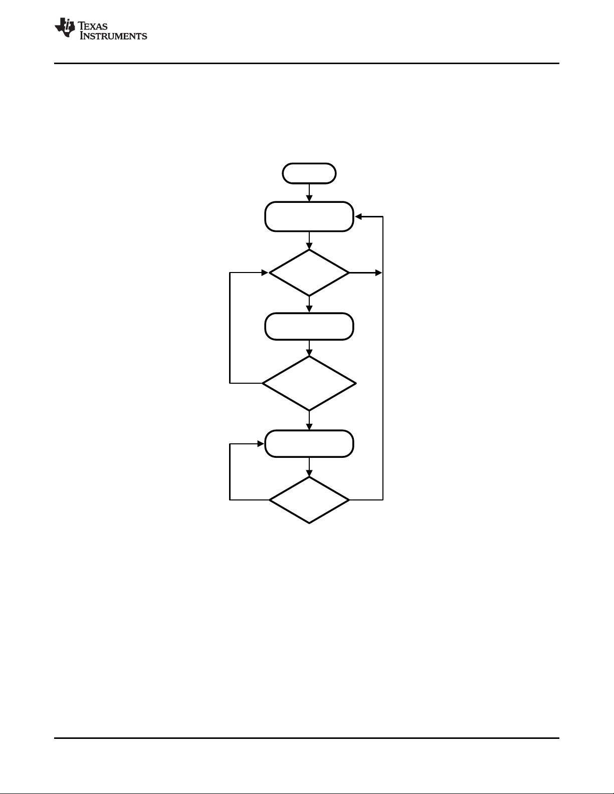
NO
NO
YES
YES
YES
Phase Error < â
PLLX
Lock Detected = False
Lock Count = 0
PLLX Lock Count =
PLLX_DLD_CNT
Phase Error > â
NO YES
START
Increment
PLLX Lock Count
PLLX
Lock Detected = True
LMK04906
www.ti.com
SNAS589F –JUNE 2012–REVISED AUGUST 2017
The digital lock detect signal can be monitored on the Status_LD or Status_Holdover pin. The pin may be
programmed to output the status of lock detect for PLL1, PLL2, or both PLL1 and PLL2.
See Digital Lock Detect Frequency Accuracy for more detailed information on programming the registers to
achieve a specified frequency accuracy in ppm with lock detect.
The digital lock detect feature can also be used with holdover to automatically exit holdover mode. See Holdover
Mode for more info.
8.3.7 Status PINS
The Status_LD, Status_HOLDOVER, Status_CLKin0, Status_CLKin1, and SYNC/Status_CLKin2 pins can be
programmed to output a variety of signals for indicating various statuses like digital lock detect, holdover, several
DAC indicators, and several PLL divider outputs.
8.3.7.1 Logic Low
This is a vary simple output. In combination with the output _MUX register, this output can be toggled between
high and low. Useful to confirm MICROWIRE programming or as a general purpose IO.
8.3.7.2 Digital Lock Detect
PLL1 DLD, PLL2 DLD, and PLL1 + PLL2 are selectable on certain output pins. See Digital Lock Detect for more
information.
Figure 10. Digital Lock Detect Flowchart
Product Folder Links: LMK04906
Submit Documentation FeedbackCopyright © 2012–2017, Texas Instruments Incorporated
29
LMK04906
SNAS589F –JUNE 2012–REVISED AUGUST 2017
www.ti.com
8.3.7.3 Holdover Status
Indicates if the device is in Holdover mode. See Holdover Mode for more information.
8.3.7.4 DAC
Various flags for the DAC can be monitored including DAC Locked, DAC Rail, DAC Low, and DAC High.
When the PLL1 tuning voltage crosses the low threshold, DAC Low is asserted. When PLL1 tuning voltage
crosses the high threshold, DAC High is asserted. When either DAC Low or DAC High is asserted, DAC Rail will
also be asserted.
DAC Locked is asserted when EN_Track = 1 and DAC is closely tracking the PLL1 tuning voltage.
8.3.7.5 PLL Divider Outputs
The PLL divider outputs are useful for debugging failure to lock issues. It allows the user to measure the
frequency the PLL inputs are receiving. The settings of PLL1_R, PLL1_N, PLL2_R, and PLL2_N output pulses at
the phase detector rate. The settings of PLL1_R / 2, PLL1_N / 2, PLL2_R / 2, and PLL2_N / 2 output a 50% duty
cycle waveform at half the phase detector rate.
8.3.7.6 CLKinX_LOS
The clock input loss of signal indicator is asserted when LOS is enabled (EN_LOS) and the clock no longer
detects an input as defined by the time-out threshold, LOS_TIMEOUT. The loss of signal indicator detects a loss
of signal on CLKinX only when CLKinX_BUF_TYPE is configured as Bipolar.
8.3.7.7 CLKinX Selected
If this clock is the currently selected/active clock, this pin will be asserted.
8.3.7.8 MICROWIRE Readback
The readback data can be output on any pin programmable to readback mode. For more information on
readback see Readback.
8.3.8 VCO
The integrated VCO uses a frequency calibration routine when register R30 is programmed to lock VCO to target
frequency. Register R30 contains the PLL2_N register.
During the frequency calibration the PLL2_N_CAL value is used instead of PLL2_N, this allows 0-delay modes to
have a separate PLL2 N value for VCO frequency calibration and regular operation.
8.3.9 Clock Distribution
8.3.9.1 Fixed Digital Delay
This section discussing Fixed Digital delay and associated registers is fundamental to understanding digital delay
and dynamic digital delay.
Clock outputs may be delayed or advanced from one another by up to 517.5 clock distribution path periods. By
programming a digital delay value from 4.5 to 522 clock distribution path periods, a relative clock output delay
from 0 to 517.5 periods is achieved. The CLKoutX_DDLY (5 to 522) and CLKoutX_HS (–0.5 or 0) registers set
the digital delay as shown in Table 3.
Table 3. Possible Digital Delay Values
CLKoutX_DDLY CLKoutX_HS Digital Delay
5 1 4.5
5 0 5
6 1 5.5
6 0 6
7 1 6.5
30
Submit Documentation Feedback Copyright © 2012–2017, Texas Instruments Incorporated
Product Folder Links: LMK04906

Digital Delay Resolution
1
2 × VCO Frequency
=
(with VCO Divider)
VCO_DIV
2 × VCO Frequency
=
LMK04906
www.ti.com
SNAS589F –JUNE 2012–REVISED AUGUST 2017
Table 3. Possible Digital Delay Values (continued)
CLKoutX_DDLY CLKoutX_HS Digital Delay
7 0 7
... ... ...
520 0 520
521 1 520.5
521 0 521
522 1 521.5
522 0 522
NOTE
Digital delay values only take effect during a SYNC event and if the NO_SYNC_CLKoutX
bit is cleared for this clock output. See Clock Output Synchronization (SYNC) for more
information.
The resolution of digital delay is determined by the frequency of the clock distribution path. The clock distribution
path is the output of Mode Mux1 (Functional Block Diagram). The best resolution of digital delay is achieved by
bypassing the VCO divider.
(2)
(3)
The digital delay between clock outputs can be dynamically adjusted with no or minimum disruption of the output
clocks. See Dynamically Programming Digital Delay for more information.
8.3.9.2 Fixed Digital Delay - Example
Given a VCO frequency of 2457.6 MHz and no VCO divider, by using digital delay the outputs can be adjusted in
1 / (2 × 2457.6 MHz) = approximately 203.5-ps steps.
To achieve quadrature (90 degree shift) between the 122.88-MHz outputs on CLKout4 and CLKout3 from a VCO
frequency of 2457.6 MHz and bypassing the VCO divider, consider the following:
1. The frequency of 122.88 MHz has a period of ~8.14 ns.
2. To delay 90 degrees of a 122.88 MHz clock period requires an approximately 2.03-ns delay.
3. Given a digital delay step of ~203.5 ps, this requires a digital delay value of 12 steps (2.03 ns / 20.35 ps =
10).
4. Since the 10 steps are half period steps, CLKout3_DDLY is programmed 5 full periods beyond 5 for a total of
10.
This result in the following programming:
• Clock output dividers to 20. CLKout2_DIV = 20 and CLKout3_DIV = 20.
• Set first clock digital delay value. CLKout2_DDLY = 5, CLKout2_HS = 0.
• Set second 90 degree shifted clock digital delay value. CLKout3_DDLY = 10, CLKout3_HS = 0.
Table 4 shows some of the possible phase delays in degrees achievable in the above example.
Product Folder Links: LMK04906
Submit Documentation FeedbackCopyright © 2012–2017, Texas Instruments Incorporated
31

LMK04906
SNAS589F –JUNE 2012–REVISED AUGUST 2017
Table 4. Relative Phase Shift from
CLKout2 to CLKout3
CLKout3_DDLY = 5 and CLKout3_HS = 0
CLKout3_DDLY CLKout_HS RELATIVE DIGITAL DELAY DEGREES of 122.88 MHz
5 1 –0.5 –9°
5 0 0 0°
6 1 0.5 9°
6 0 1 18°
7 1 1.5 27°
7 0 2 36°
8 1 2.5 45°
8 0 3 54°
9 1 3.5 63°
9 0 4 72°
10 1 4.5 81°
10 0 5 90°
11 1 5.5 99°
11 0 6 108°
12 1 6.5 117°
12 0 7 126°
13 1 7.5 135°
13 0 8 144°
14 1 8.5 153°
— — — —
www.ti.com
Figure 12 illustrates clock outputs programmed with different digital delay values during a SYNC event.
See Dynamically Programming Digital Delay for more information on dynamically adjusting digital delay.
8.3.9.3 Clock Output Synchronization (SYNC)
The purpose of the SYNC function is to synchronize the clock outputs with a fixed and known phase relationship
between each clock output selected for SYNC. SYNC can also be used to hold the outputs in a low or 0 state.
The NO_SYNC_CLKoutX bits can be set to disable synchronization for a clock output.
To enable SYNC, EN_SYNC must be set. See EN_SYNC, Enable Synchronization.
The digital delay value set by CLKoutX_DDLY takes effect only upon a SYNC event. The digital delay due to
CLKoutX_HS takes effect immediately upon programming. See Dynamically Programming Digital Delay for more
information on dynamically changing digital delay.
During a SYNC event, clock outputs driven by the VCO are not synchronized to clock outputs driven by OSCin.
OSCout0 is always driven by OSCin. CLKout3 or 4 may be driven by OSCin depending on the
CLKoutX_OSCin_Sel bit value. While SYNC is asserted, NO_SYNC_CLKoutX operates normally for CLKout3
and 4 under all circumstances. SYNC operates normally for CLKout3 and 4 when driven by VCO.
8.3.9.3.1 Effect of SYNC
When SYNC is asserted, the outputs to be synchronized are held in a logic low state. When SYNC is
unasserted, the clock outputs to be synchronized are activated and will transition to a high state simultaneously
with one another except where different digital delay values have been programmed.
See Dynamically Programming Digital Delay for SYNC functionality when SYNC_QUAL = 1.
32
Submit Documentation Feedback Copyright © 2012–2017, Texas Instruments Incorporated
Product Folder Links: LMK04906

LMK04906
www.ti.com
SNAS589F –JUNE 2012–REVISED AUGUST 2017
Table 5. Steady State Clock Output Condition
Given Specified Inputs
SYNC_TYPE SYNC_POL
_INV
0,1,2 (Input) 0 0 Active
0,1,2 (Input) 0 1 Low
0,1,2 (Input) 1 0 Low
0,1,2 (Input) 1 1 Active
3, 4, 5, 6 (Output) 0 0 or 1 Active
3, 4, 5, 6 (Output) 1 0 or 1 Low
8.3.9.3.2 Methods of Generating SYNC
SYNC PIN CLOCK OUTPUT STATE
There are five methods to generate a SYNC event:
• Manual:
– Asserting the SYNC pin according to the polarity set by SYNC_POL_INV.
– Toggling the SYNC_POL_INV bit though MICROWIRE will cause a SYNC to be asserted.
• Automatic:
– If PLL1_SYNC_DLD or PLL2_SYNC_DLD is set, the SYNC pin will be asserted while DLD (digital lock
detect) is false for PLL1 or PLL2 respectively.
– Programming Register R30, which contains PLL2_N will generate a SYNC event when using the internal
VCO.
– Programming Register R0 through R5 when SYNC_EN_AUTO = 1.
NOTE
Due to the speed of the clock distribution path (as fast as approximately 325-ps period)
and the slow slew rate of the SYNC, the exact VCO cycle at which the SYNC is asserted
or unasserted by the SYNC is undefined. The timing diagrams show a sharp transition of
the SYNC to clarify functionality.
8.3.9.3.3 Avoiding Clock Output Interruption Due to SYNC
Any CLKout outputs that have their NO_SYNC_CLKoutX bits set will be unaffected by the SYNC event. It is
possible to perform a SYNC operation with the NO_SYNC_CLKoutX bits cleared, then set the
NO_SYNC_CLKoutX bits so that the selected clocks will not be affected by a future SYNC. Future SYNC events
will not effect these clocks but will still cause the newly synchronized clocks to be re-synchronized using the
currently programmed digital delay values. When this happens, the phase relationship between the first group of
synchronized clocks and the second group of synchronized clocks will be undefined unless the SYNC pulse is
qualified by an output clock. See Dynamically Programming Digital Delay.
8.3.9.3.4 SYNC Timing
When discussing the timing of the SYNC function, one cycle refers to one period of the clock distribution path.
Product Folder Links: LMK04906
Submit Documentation FeedbackCopyright © 2012–2017, Texas Instruments Incorporated
33

Distribution
Path
SYNC
(SYNC_POL
_INV=1)
CLKout0
CLKout2
CLKout4
A B C
D
6 cycles
6 cycles
CLKoutX_DDLY &
CLKoutX_HS
LMK04906
SNAS589F –JUNE 2012–REVISED AUGUST 2017
CLKout0_DIV = 0(valid only for external VCO mode)
CLKout2_DIV = 2
CLKout4_DIV = 4
The digital delay for all clock outputs is 5
The digital delay half step for all clock outputs is 0
SYNC_QUAL = 0 (No qualification)
Figure 11. Clock Output Synchronization Using the SYNC Pin (Active Low)
www.ti.com
See Figure 11 during this discussion on the timing of SYNC. SYNC must be asserted for greater than one clock
cycle of the clock distribution path to latch the SYNC event. After SYNC is asserted, the SYNC event is latched
on the rising edge of the distribution path clock, at time A. After this event has been latched, the outputs will not
reflect the low state for 6 cycles, at time B. Due to the asynchronous nature of SYNC with respect to the output
clocks, it is possible that a glitch pulse could be created when the clock output goes low from the SYNC event.
This is shown by CLKout4 in Figure 11 and CLKout2 in Figure 12. See Relative Dynamic Digital Delay for more
information on synchronizing relative to an output clock to eliminate or minimize this glitch pulse.
After SYNC becomes unasserted the event is latched on the following rising edge of the distribution path clock,
time C. The clock outputs will rise at time D, coincident with a rising distribution clock edge that occurs after 6
cycles plus as many more cycles as programmed by the digital delay for that clock output. Therefore, the
soonest a clock output will become high is 11 cycles after the SYNC unassertion event registration, time C, when
the smallest digital delay value of 5 is set. If CLKoutX_HS = 1 and CLKoutX_DDLY = 5, then the clock output will
rise 10.5 cycles after SYNC is unassertion event registration.
34
Submit Documentation Feedback Copyright © 2012–2017, Texas Instruments Incorporated
Product Folder Links: LMK04906

Distribution
Path
SYNC
(SYNC_POL
_INV=1)
CLKout0
CLKout2
CLKout4
C D
CLKout5
E F
6 cycles
6 cycles
CLKoutX_DDLY & CLKoutX_HS
4.5
cycles
2.5
cycles
1 cycle
www.ti.com
LMK04906
SNAS589F –JUNE 2012–REVISED AUGUST 2017
CLKout0_DIV = 2, CLKout0_DDLY = 5
CLKout2_DIV = 4, CLKout2_DDLY = 7
CLKout4_DIV = 4, CLKout4_DDLY = 8
CLKout5_DIV = 4, CLKour4_DDLY = 8
CLKout0_HS = 1
CLKout2_HS = 0
CLKout4_HS = 0
CLKout5_HS = 0
SYNC_QUAL = 0 (No qualification)
Figure 12. Clock Output Synchronization Using the SYNC Pin (Active Low)
Figure 12 illustrates the timing with different digital delays programmed.
• Time A) SYNC assertion event is latched.
• Time B) SYNC unassertion latched.
• Time C) All outputs toggle and remain low. A glitch pulse can occur at this time as shown by CLKout2.
• Time D) After 6 + 4.5 = 10.5 cycles CLKout0 rises. This is the shortest time from SYNC unassertion
registration to clock rising edge possible.
• Time E) After 6 + 7 = 13 cycles CLKout2 rises. CLKout2 and CLKout4, 5 are programmed for quadrature
operation.
• Time F) After 6 + 8 = 14 cycles CLKout4 and 5 rise.
8.3.9.4 Dynamically Programming Digital Delay
To use dynamic digital delay synchronization qualification set SYNC_QUAL = 1. This causes the SYNC pulse to
be qualified by a clock output so that the SYNC event occurs after a specified time from a clock output transition.
This allows the relative adjustment of clock output phase in real-time with no or minimum interruption of clock
outputs. Hence the term dynamic digital delay.
Note that changing the phase of a clock output requires momentarily altering in the rate of change of the clock
output phase and therefore by definition results in a frequency distortion of the signal.
Without qualifying the SYNC with an output clock, the newly synchronized clocks would have a random and
unknown digital delay (or phase) with respect to clock outputs not currently being synchronized.
8.3.9.4.1 Absolute vs Relative Dynamic Digital Delay
The clock used for qualification of SYNC is selected with the feedback mux (FEEDBACK_MUX).
Submit Documentation FeedbackCopyright © 2012–2017, Texas Instruments Incorporated
Product Folder Links: LMK04906
35

LMK04906
SNAS589F –JUNE 2012–REVISED AUGUST 2017
www.ti.com
If the clock selected by the feedback mux has its NO_SYNC_CLKoutX = 1, then an absolute dynamic digital
delay adjustment will be performed during a SYNC event and the digital delay of the feedback clock will not be
adjusted.
If the clock selected by the feedback mux has its NO_SYNC_CLKoutX = 0, then a self-referenced or relative
dynamic digital delay adjustment will be performed during a SYNC event and the digital delay of the feedback
clock will be adjusted.
Clocks with NO_SYNC_CLKoutX = 1 always operate without interruption.
8.3.9.4.2 Dynamic Digital Delay and 0-Delay Mode
When using a 0-delay mode absolute dynamic digital delay is recommended. Using relative dynamic digital
delay with a 0-delay mode may result in a momentary clock loss on the adjusted clock also being used for 0delay feedback that may result in PLL1 DLD becoming low. This may result in HOLDOVER mode being activated
depending upon device configuration.
8.3.9.4.3 SYNC and Minimum Step Size
The minimum step size adjustment for digital delay is half a clock distribution path cycle. This is achieved by
using the CLKoutX_HS bit. The CLKoutX_HS bit change effect is immediate without the need for SYNC. To shift
digital delay using CLKoutX_DDLY a SYNC signal must be generated for the change to take effect.
8.3.9.4.4 Programming Overview
To dynamically adjust the digital delay with respect to an existing clock output the device should be programmed
as follows:
• Set SYNC_QUAL = 1 for clock output qualification.
• Set CLKout2_PD = 0. Required for proper operation of SYNC_QUAL = 1.
• Set EN_FEEDBACK_MUX = 1 to enable the feedback buffer.
• Set FEEDBACK_MUX to the clock output that the newly synchronized clocks will be qualified by.
• Set NO_SYNC_CLKoutX = 1 for the output clocks that will continue to operate during the SYNC event. There
is no interruption of output on these clocks.
– If FEEDBACK_MUX selects a clock output with NO_SYNC_CLKoutX = 1, then absolute dynamic digital
delay is performed.
– If FEEDBACK_MUX selects a clock output with NO_SYNC_CLKoutX = 0, then self-referenced or relative
dynamic digital delay is performed.
• The SYNC_EN_AUTO bit may be set to cause a SYNC event to begin when register R0 to R5 is
programmed. The auto SYNC feature is a convenience since does not require the application to manually
assert SYNC by toggling the SYNC_POL_INV bit or the SYNC pin when changing digital delay. However,
under the following condition a special programming sequence is required if SYNC_EN_AUTO = 1:
– The CLKoutX_DDLY value being set in the programmed register is 13 or more.
• Under the following condition a SYNC_EN_AUTO must = 0:
– If the application requires a digital delay resolution of half a clock distribution path cycle in relative
dynamic digital delay mode because the HS bit must be fixed per Table 6 for a qualifying clock.
8.3.9.4.5 Internal Dynamic Digital Delay Timing
To dynamically adjust digital delay a SYNC must occur. Once the SYNC is qualified by an output clock, 3 cycles
later an internal one shot pulse will occur. The width of the one shot pulse is 3 cycles. This internal one shot
pulse will cause the outputs to turn off and then back on with a fixed delay with respect to the falling edge of the
qualification clock. This allows for dynamic adjustments of digital delay with respect to an output clock.
The qualified SYNC timing is shown in Figure 13 for absolute dynamic digital delay and Figure 14 for relative
dynamic digital delay.
8.3.9.4.6 Other Timing Requirements
When adjusting digital delay dynamically, the falling edge of the qualifying clock selected by the
FEEDBACK_MUX must coincide with the falling edge of the clock distribution path. For this requirement to be
met, program the CLKoutX_HS value of the qualifying clock output according to Table 6.
36
Submit Documentation Feedback Copyright © 2012–2017, Texas Instruments Incorporated
Product Folder Links: LMK04906

LMK04906
www.ti.com
SNAS589F –JUNE 2012–REVISED AUGUST 2017
Table 6. Half Step Programming Requirement of Qualifying Clock During SYNC Event
DISTRIBUTION PATH FREQUENCY CLKoutX_DIV value CLKoutX_HS
≥ 1.8 GHz
< 1.8 GHz
Even Must = 1 during SYNC event.
Odd Must = 0 during SYNC event.
Even Must = 0 during SYNC event.
Odd Must = 1 during SYNC event.
8.3.9.5 Absolute Dynamic Digital Delay
Absolute dynamic digital delay can be used to program a clock output to a specific phase offset from another
clock output.
Pros:
• Simple direct phase adjustment with respect to another clock output.
• CLKoutX_HS will remain constant for qualifying clock.
– Can easily use auto sync feature (SYNC_EN_AUTO = 1) when digital delay adjustment requires half step
digital delay requirements.
• Can be used with 0-delay mode.
Cons:
• For some phase adjustments there may be a glitch pulse due to SYNC assertion.
– For example see CLKout4 in Figure 11 and CLKout2 in Figure 12.
8.3.9.5.1 Absolute Dynamic Digital Delay - Example
To illustrate the absolute dynamic digital delay adjust procedure, consider the following example.
System Requirements:
• VCO Frequency = 2457.6 MHz
• CLKout0 = 819.2 MHz (CLKout0_DIV = 3)
• CLKout2 = 307.2 MHz (CLKout2_DIV = 8)
• CLKout4 = 245.76 MHz (CLKout4_DIV = 10)
• For all clock outputs during initial programming:
– CLKoutX_DDLY = 5
– CLKoutX_HS = 1
– NO_SYNC_CLKoutX = 0
The application requires the 307.2 MHz clock to be stepped in 22.5 degree steps (approximately 203.4 ps),
which is the minimum step resolution allowable by the clock distribution path requiring use of the half step bit
(CLKoutX_HS). That is 1 / 2457.6 MHz / 2 = ~203.4 ps. During the stepping of the 307.2 MHz clock the 819.2
MHz and 245.76 MHz clock must not be interrupted.
1. The device is programmed from register R0 to R30 with values that result in the device being locked and
operating as desired, see the system requirements above. The phase of all the output clocks are aligned
because all the digital delay and half step values were the same when the SYNC was generated by
programming register R30. The timing of this is as shown in Figure 11.
2. Now the registers will be programmed to prepare for changing digital delay (or phase) dynamically.
Table 7. Register Setup for Absolute Dynamic Digital Delay Example
REGISTER PURPOSE
SYNC_QUAL = 1
EN_SYNC = 1 (default) Required for SYNC functionality.
CLKout2_PD = 0
EN_FEEDBACK_MUX = 1
FEEDBACK_MUX = 2 (CLKout4) Use the fixed 245.76 MHz clock as the SYNC qualification clock.
Use a clock output for qualifying the SYNC pulse for dynamically
adjusting digital delay.
Required when SYNC_QUAL = 1.
CLKout2 outputs may be powered down or in use.
Enable the feedback mux for SYNC operation for dynamically
adjusting digital delay.
Product Folder Links: LMK04906
Submit Documentation FeedbackCopyright © 2012–2017, Texas Instruments Incorporated
37

LMK04906
SNAS589F –JUNE 2012–REVISED AUGUST 2017
www.ti.com
Table 7. Register Setup for Absolute Dynamic Digital Delay Example (continued)
REGISTER PURPOSE
NO_SYNC_CLKout0 = 1
NO_SYNC_CLKout4 = 1
CLKout4_HS = 1
SYNC_EN_AUTO = 1 Automatic generation of SYNC is allowed for this case.
This clock output (819.2 MHz) won't be affected by SYNC. It will
always operate without interruption.
This clock output (245.76 MHz) won't be affected by SYNC. It will
always operate without interruption.
This clock will also be the qualifying clock in this example.
Since CLKout4 is the qualifying clock and CLKoutX_DIV is even, the
half step bit must be set to 1. See Table 6.
After the registers in Table 7 have been programmed, the application may now dynamically adjust the digital
delay of CLKout2 (307.2 MHz).
3. Adjust digital delay of CLKout2.
See Table 8 for the programming values to set a specified phase offset from the absolute reference clock.
Table 8 is dependant upon the qualifying clock divide value of 12, see Calculating Dynamic Digital Delay Values
For Any Divide for information on creating tables for any divide value.
Table 8. Programming for Absolute Digital Delay Adjustment
DEGREES OF ADJUSTMENT FROM INITIAL 307.2-MHZ PHASE PROGRAMMING
±0 or ±360 degrees CLKout2_DDLY = 14; CLKout2_HS = 1
22.5° –337.5° CLKout2_DDLY = 14; CLKout2_HS = 0
45° –315° CLKout2_DDLY = 15; CLKout2_HS = 1
67.5° –292.54° CLKout2_DDLY = 5; CLKout2_HS = 0
90° –270° CLKout2_DDLY = 6; CLKout2_HS = 1
112.5° –247.5° CLKout2_DDLY = 6; CLKout2_HS = 0
135° –25° CLKout2_DDLY = 7; CLKout2_HS = 1
157.5° –202.5° CLKout2_DDLY = 7; CLKout2_HS = 0
180° –180° CLKout2_DDLY = 8; CLKout2_HS = 1
247.5° –112.5° CLKout2_DDLY = 8; CLKout2_HS = 0
270° –90° CLKout2_DDLY = 9; CLKout2_HS = 1
292.5° –67.5° CLKout2_DDLY = 9; CLKout2_HS = 0
315° –45° CLKout2_DDLY = 10; CLKout2_HS = 1
337.5° –22.5° CLKout2_DDLY = 10; CLKout2_HS = 0
After setting the new digital delay values, the act of programming R1 will start a SYNC automatically because
SYNC_EN_AUTO = 1.
If the user elects to reduce the number of SYNCs because they are not required when only CLKout2_HS is set,
then SYNC_EN_AUTO is = 0 and the SYNC may now be generated by toggling the SYNC pin or by toggling the
SYNC_POL_INV bit. Because of the internal one shot pulse, no strict timing of the SYNC pin or SYNC_POL_INV
bit is required.
After the SYNC event, the clock output will adjust according to Table 8. See Figure 13 for a detailed view of the
timing diagram. The timing diagram critical points are:
• Time A) SYNC assertion event is latched.
• Time B) First qualifying falling clock output edge.
• Time C) Second qualifying falling clock output edge.
• Time D) Internal one shot pulse begins. 5 cycles later clock outputs will be forced low
• Time E) Internal one shot pulse ends. 5.5 cycles + digital delay cycles later the synced clock outputs rise.
• Time F) Clock outputs are forced low. (CLKout2 is already low).
• Time G) Beginning of digital delay cycles.
• Time H) For CLKout2_DDLY = 14; the clock output rises now.
38
Submit Documentation Feedback Copyright © 2012–2017, Texas Instruments Incorporated
Product Folder Links: LMK04906

Distribution
Path
Internal One
Shot Pulse
5 cycles
CLKoutX_DDLY and CLKoutX_HS
3 cycles
SYNC
5.5 cycles
AB C D E F G
CLKout0 /3
HS = 1
CLKout2 /8
HS = 1
CLKout4 /10
HS = 1
3 cycles
H
13.5 cycles
2
1
www.ti.com
LMK04906
SNAS589F –JUNE 2012–REVISED AUGUST 2017
(SYNC_QUAL = 1, Qualify with clock output)
Figure 13. Absolute Dynamic Digital Delay Programming Example
8.3.9.6 Relative Dynamic Digital Delay
Relative dynamic digital delay can be used to program a clock output to a specific phase offset from another
clock output.
Pros:
• Simple direct phase adjustment with respect to same clock output.
• The clock output will always behave the same during digital delay adjustment transient. For some divide
values there will be no glitch pulse.
Cons:
• For some clock divide values there may be a glitch pulse due to SYNC assertion.
• Adjustments of digital delay requiring the half step bit (CLKoutX_HS) for finer digital delay adjust is
complicated.
• Use with 0-delay mode may result in PLL1 DLD becoming low and HOLDOVER mode becoming activated.
– DISABLE_DLD1_DET can be set to prevent HOLDOVER from becoming activated due to PLL1 DLD
becoming low.
8.3.9.6.1 Relative Dynamic Digital Delay - Example
To illustrate the relative dynamic digital delay adjust procedure, consider the following example.
System Requirements:
• VCO Frequency = 2457.6 MHz
• CLKout0 = 819.2 MHz (CLKout0_DIV = 3)
• CLKout2 = 491.52 MHz (CLKout2_DIV = 5)
• CLKout4 = 491.52 MHz (CLKout4_DIV = 5)
• For all clock outputs during initial programming:
– CLKoutX_DDLY = 5
– CLKoutX_HS = 0
– NO_SYNC_CLKoutX = 0
Submit Documentation FeedbackCopyright © 2012–2017, Texas Instruments Incorporated
Product Folder Links: LMK04906
39

LMK04906
SNAS589F –JUNE 2012–REVISED AUGUST 2017
www.ti.com
The application requires the 491.52 MHz clock to be stepped in 22.5degree steps (~203.4 ps), which is the
minimum step resolution allowable by the clock distribution path. That is 1 / 2457.62 MHz / 2 = ~203.4 ps. During
the stepping of the 491.52 MHz clocks the 819.2 MHz clock must not be interrupted.
1. The device is programmed from register R0 to R30 with values that result in the device being locked and
operating as desired, see the system requirements above. The phase of all the output clocks are aligned
because all the digital delay and half step values were the same when the SYNC was generated by
programming register R30. The timing of this is as shown in Figure 11.
2. Now the registers will be programmed to prepare for changing digital delay (or phase) dynamically.
Table 9. Register Setup for Relative Dynamic Digital Delay Adjustment
REGISTER PURPOSE
SYNC_QUAL = 1
EN_SYNC = 1 (default) Required for SYNC functionality.
CLKout2_PD = 0
EN_FEEDBACK_MUX = 1
FEEDBACK_MUX = 1 (CLKout2) Use the clock itself as the SYNC qualification clock.
NO_SYNC_CLKout0 = 1
NO_SYNC_CLKout4 = 1 CLKout4’s phase is not to change with respect to CLKout0.
SYNC_EN_AUTO = 0 (default)
Use clock output for qualifying the SYNC pulse for dynamically
adjusting digital delay.
Required when SYNC_QUAL = 1.
CLKout2 outputs may be powered down or in use.
Enable the feedback mux for SYNC operation for dynamically
adjusting digital delay.
This clock output (819.2 MHz) won't be affected by SYNC. It will
always operate without interruption.
Automatic generation of SYNC is not allowed because of the half
step requirement in relative dynamic digital delay mode.
SYNC must be generated manually by toggling the SYNC_POL_INV
bit or the SYNC pin.
After the above registers have been programmed, the application may now dynamically adjust the digital
delay of the 491.52 MHz clocks.
3. Adjust digital delay of CLKout2 by one step which is 22.5 degrees or approximately 203.4 ps.
See Table 10 for the programming sequence to step one half clock distribution period forward or backwards.
Refer to Calculating Dynamic Digital Delay Values For Any Divide for more information on how to calculate digital
delay and half step values for other cases.
To fulfill the qualifying clock output half step requirement in Table 6 when dynamically adjusting digital delay, the
CLKoutX_HS bit must be cleared for clocks with even divides. So before any dynamic digital delay adjustment,
CLKoutX_HS must be clear because the clock divide value is even. To achieve the final required digital delay
adjustment, the CLKoutX_HS bit may set after SYNC.
Table 10. Programming Sequence for One Step Adjust
STEP DIRECTION AND CURRENT HS STATE PROGRAMMING SEQUENCE
Adjust clock output one step forward.
CLKout2_HS is 0.
Adjust clock output one step forward.
CLKout2_HS is 1.
Adjust clock output one step backward.
CLKout2_HS is 0.
Adjust clock output one step backward.
CLKout2_HS is 1.
1. CLKout2_HS = 1.
1. CLKout2_DDLY = 11.
2. Perform SYNC event.
3. CLKout2_HS = 0.
1. CLKout2_HS = 1.
2. CLKout2_DDLY =11.
3. Perform SYNC event.
1. CLKout2_HS = 0.
After programing the updated CLKout2_DDLY and CLKout2_HS values, perform a SYNC event. The SYNC may
be generated by toggling the SYNC pin or by toggling the SYNC_POL_INV bit. Because of the internal one shot
pulse, no strict timing of the SYNC pin or SYNC_POL_INV bit is required. After the SYNC event, the clock output
will be at the specified phase. See Figure 14 for a detailed view of the timing diagram. The timing diagram critical
points are:
• Time A) SYNC assertion event is latched.
40
Submit Documentation Feedback Copyright © 2012–2017, Texas Instruments Incorporated
Product Folder Links: LMK04906

Distribution
Path
Shot Pulse
5 cycles
CLKoutX_DDLY and
CLKoutX_HS
10.5
cycles
3 cycles
SYNC
5.5 cycles
B C D E F G
CLKout0 /3
HS = 1
CLKout2 /5
HS = 1
CLKout4 /5
HS = 1
3 cycles
2
A
1
LMK04906
www.ti.com
SNAS589F –JUNE 2012–REVISED AUGUST 2017
• Time B) First qualifying falling clock output edge.
• Time C) Second qualifying falling clock output edge.
• Time D) Internal one shot pulse begins. 5 cycles later clock outputs will be forced low.
• Time E) Internal one shot pulse ends. 5.5 cycles + digital delay cycles later the synced clock outputs rise.
• Time F) Clock outputs are forced low. (CLKouts are already low).
• Time G) Beginning of digital delay cycles.
• Time H) For CLKout2_DDLY = 11; the clock output rises now.
(SYNC_QUAL = 1, Qualify with clock output)
Starting condition is after half step is removed (CLKout2_HS = 0).
Figure 14. Relative Dynamic Digital Delay Programming Example—2nd Adjust
8.3.10 0-Delay Mode
When 0-delay mode is enabled the clock output selected by the Feedback Mux is connected to the PLL1 N
counter to ensure a fixed phase relationship between the selected CLKin and the fed back CLKout. When all the
clock outputs are synced together, all the clock outputs will share the same fixed phase relationship between the
selected CLKin and the fed back CLKout. The feedback can be internal or external using FBCLKin port.
When 0-delay mode is enabled the lowest frequency clock output is fed back to the Feedback Mux to ensure a
repeatable fixed CLKin to CLKout phase relationship between all clock outputs.
If a clock output that is not the lowest frequency output is selected for feedback, then clocks with lower
frequencies will have an unknown phase relationship with respect the other clocks and clock input. There will be
a number of possible phase relationships equal to Feedback_Clock_Frequency / Lower_Clock_Frequency that
may occur.
The Feedback Mux can select a clock output of some of the clocks for internal feedback or the FBCLKin port for
external 0-delay feedback.
To use 0-delay mode, the bit EN_FEEDBACK_MUX must be set (=1) to power up the feedback mux.
See PLL Programming for more information on programming PLL1_N for 0-delay mode.
When using an external VCO mode, internal 0-delay feedback must be used since the FBCLKin port is shared
with the Fin input.
Table 11 outlines several registers to program for 0-delay mode.
Submit Documentation FeedbackCopyright © 2012–2017, Texas Instruments Incorporated
Product Folder Links: LMK04906
41

LMK04906
SNAS589F –JUNE 2012–REVISED AUGUST 2017
www.ti.com
Table 11. Programming 0-Delay Mode
REGISTER PURPOSE
MODE = 2 or 5 Select one of the 0-delay modes for device.
EN_FEEDBACK_MUX = 1 Enable feedback mux.
FEEDBACK_MUX = Application Specific Select CLKout or FBCLKin for 0-delay feedback.
CLKoutX_DIV
PLL1_N PLL1_N value used with CLKoutX_DIV in loop.
The divide value of the clock selected by FEEDBACK_MUX is
important for PLL2 N value calculation
8.3.11 Hitless Switching
The LMK04906 supports hitless switching.
8.4 Device Functional Modes
8.4.1 Mode Selection
The LMK04906 family is capable of operating in several different modes as programmed by MODE: Device
Mode.
Table 12. Device Mode Selection
MODE
R11[31:27]
0 X X Internal X
2 X X Internal X X
3 X X External X
5 X X External X X
6 X Internal X
8 X Internal X X
11 X External X
16 X
PLL1 PLL2 PLL2 VCO 0-DELAY CLOCK DIST
In addition to selecting the device's mode of operation above, some modes require additional configuration. Also
there are other features including holdover and dynamic digital delay that can also be enabled.
Table 13. Registers to Further Configure Device Mode of Operation
DYNAMIC DIGITAL
DELAY
42
REGISTER HOLDOVER 0-DELAY
HOLDOVER_MODE 2 — —
EN_TRACK User — —
DAC_CLK_DIV User — —
EN_MAN_DAC User — —
DISABLE_DLD1_DET User — —
EN_VTUNE_RAIL_
DET
DAC_HIGH_TRIP User — —
DAC_LOW_TRIP User — —
FORCE_HOLDOVER 0 — —
SYNC_EN_AUTO — — User
SYNC_QUAL — — 1
EN_SYNC — — 1
CLKout2_PD — — 0
EN_
FEEDBACK_MUX
Submit Documentation Feedback Copyright © 2012–2017, Texas Instruments Incorporated
Product Folder Links: LMK04906
User — —
— 1 1

R
CLKinX
CLKinX*
N
Phase
Detector
PLL1
External VCXO
or Tunable
Crystal
R
N
Phase
Detector
PLL2
Internal
VCO
External
Loop Filter
OSCin
CPout1
OSCout0
OSCout0*
LMK04906
CPout2
Partially
Integrated
Loop Filter
6 outputs
External
Loop Filter
PLL1 PLL2
6 blocks
1 output
3 inputs
Input
Buffer
CLKoutX
CLKoutX*
Divider
Digital Delay
Analog Delay
Copyright © 2016, Texas Instruments Incorporated
LMK04906
www.ti.com
SNAS589F –JUNE 2012–REVISED AUGUST 2017
Table 13. Registers to Further Configure Device Mode of Operation (continued)
REGISTER HOLDOVER 0-DELAY
FEEDBACK_MUX — Feedback Clock Qualifying Clock
NO_SYNC_
CLKoutX
— — User
DYNAMIC DIGITAL
DELAY
8.4.2 Operating Modes
The LMK04906 is a flexible device that can be configured for many different use cases. The following simplified
block diagrams help show the user the different use cases of the device.
8.4.2.1 Dual PLL
Figure 15 illustrates the typical use case of the LMK04906 in dual loop mode. In dual loop mode the reference to
PLL1 is either CLKin0, CLKin1, or CLKin2. An external VCXO or tunable crystal will be used to provide feedback
for the first PLL and a reference to the second PLL. This first PLL cleans the jitter with the VCXO or low cost
tunable crystal by using a narrow loop bandwidth. The VCXO or tunable crystal output may be buffered through
the OSCout0 port and optionally on up to 2 of the CLKouts. The VCXO or tunable crystal is used as the
reference to PLL2 and may be doubled using the frequency doubler. The internal VCO drives up to six
divide/delay blocks which drive 6 clock outputs.
Holdover functionality is optionally available when the input reference clock is lost. Holdover works by fixing the
tuning voltage of PLL1 to the VCXO or tunable crystal.
It is also possible to use an external VCO in place of PLL2's internal VCO.
Figure 15. Simplified Functional Block Diagram for Dual Loop Mode
8.4.2.2 0-Delay Dual PLL
Figure 16 illustrates the use case of 0-delay dual loop mode. This configuration is very similar to Dual PLL except
that the feedback to the first PLL is driven by a clock output. This causes the clock outputs to have deterministic
phase with the clock input. Since all the clock outputs can be synchronized together, all the clock outputs can be
in phase with the clock input signal. The feedback to PLL1 can be connected internally as shown, or externally
using FBCLKin (CLKin1) as an input port.
It is also possible to use an external VCO in place of PLL2's internal VCO.
Product Folder Links: LMK04906
Submit Documentation FeedbackCopyright © 2012–2017, Texas Instruments Incorporated
43

R
N
Phase
Detector
PLL2
Internal
VCO
OSCin
OSCout0
OSCout0*
LMK04906
CPout2
Partially
Integrated
Loop Filter
6 outputs
External
Loop Filter
PLL2
6 blocks
1 outputs
OSCin*
CLKoutX
CLKoutX*
Divider
Digital Delay
Analog Delay
R
CLKinX
CLKinX*
Phase
Detector
PLL1
External VCXO
or Tunable
Crystal
R
N
Phase
Detector
PLL2
Internal
VCO
External
Loop Filter
Input
Buffer
CPout1
OSCout0
OSCout0*
LMK04906
CPout2
Partially
Integrated
Loop Filter
6 outputs
External
Loop Filter
PLL1 PLL2
6 blocks
1 output
3 inputs
N
OSCin
Internal or external loopback, user programmable
CLKoutX
CLKoutX*
Divider
Digital Delay
Analog Delay
LMK04906
SNAS589F –JUNE 2012–REVISED AUGUST 2017
www.ti.com
Figure 16. Simplified Functional Block Diagram for 0-delay Dual Loop Mode
8.4.2.3 Single PLL
Figure 17 illustrates the use case of single PLL mode. In single PLL mode only PLL2 is used and PLL1 is
powered down. OSCin is used as the reference input. The internal VCO drives up to 6 divide/delay blocks which
drive 6 clock outputs. The reference at OSCin can be used to drive the OSCout0 port. OSCin can also optionally
drive up to 2 of the clock outputs.
It is also possible to use an external VCO in place of PLL2's internal VCO.
Figure 17. Simplified Functional Block Diagram for Single Loop Mode
8.4.2.4 0-delay Single PLL
Figure 18 illustrates the use case of 0-delay single PLL mode. This configuration is very similar to Single PLL
except that the feedback to PLL2 comes from a clock output. This causes the clock outputs to be in phase with
the reference input. Since all the clock outputs can be synchronized together, all the clock outputs can be in
phase with the clock input signal. The feedback to PLL2 can be performed internally as shown, or externally
using FBCLKin (CLKin1) as an input port.
It is also possible to use an external VCO in place of PLL2's internal VCO.
Product Folder Links: LMK04906
44
Submit Documentation Feedback Copyright © 2012–2017, Texas Instruments Incorporated

CLKin1
CLKin1*
OSCin
OSCout0
OSCout0*
LMK04906
OSCin*
6 outputs
6 blocks
1 output
CLKoutX
CLKoutX*
Divider
Digital Delay
Analog Delay
R
N
Phase
Detector
PLL2
Internal
VCO
OSCin
OSCout0
OSCout0*
LMK04906
CPout2
Partially
Integrated
Loop Filter
6 outputs
External
Loop Filter
PLL2
6 blocks
1 output
OSCin*
Internal or external loopback, user programmable
CLKoutX
CLKoutX*
Divider
Digital Delay
Analog Delay
LMK04906
www.ti.com
SNAS589F –JUNE 2012–REVISED AUGUST 2017
Figure 18. Simplified Functional Block Diagram for 0-delay Single Loop Mode
8.4.2.5 Clock Distribution
Figure 19 illustrates the LMK04906 used for clock distribution. CLKin1 is used to drive up to 6 divide/delay blocks
which drive 6 outputs. OSCin can be used to drive the OSCout port. OSCin can also optionally drive up to 2 of
the clock outputs.
Figure 19. Simplified Functional Block Diagram for Mode Clock Distribution
8.5 Programming
LMK04906 devices are programmed using 32-bit registers. Each register consists of a 5-bit address field and 27bit data field. The address field is formed by bits 0 through 4 (LSBs) and the data field is formed by bits 5 through
31 (MSBs). The contents of each register is clocked in MSB first (bit 31), and the LSB (bit 0) last. During
programming, the LEuWire signal should be held low. The serial data is clocked in on the rising edge of the
CLKuWire signal. After the LSB (bit 0) is clocked in the LEuWire signal should be toggled low-to-high-to-low to
latch the contents into the register selected in the address field. It is recommended to program registers in
numeric order, for example R0 to R16, and R24 to R31 to achieve proper device operation. Figure 6 illustrates
the serial data timing sequence.
To achieve proper frequency calibration, the OSCin port must be driven with a valid signal before programming
register R30. Changes to PLL2 R divider or the OSCin port frequency require register R30 to be reloaded in
order to activate the frequency calibration process.
8.5.1 Special Programming Case for R0 to R5 for CLKoutX_DIV and CLKoutX_DDLY
In some cases when programming register R0 to R5 to change the CLKoutX_DIV divide value or
CLKoutX_DDLY delay value, 3 additional CLKuWire cycles must occur after loading the register for the newly
programmed divide or delay value to take effect. These special cases include:
• When CLKoutX_DIV is > 25.
• When CLKoutX_DDLY is > 12. Note, loading the digital delay value only prepares for a future SYNC event.
Product Folder Links: LMK04906
Submit Documentation FeedbackCopyright © 2012–2017, Texas Instruments Incorporated
45

LMK04906
SNAS589F –JUNE 2012–REVISED AUGUST 2017
www.ti.com
Programming (continued)
Also, since SYNC_EN_AUTO bit = 1 automatically generates a SYNC on the falling edge of LE when R0 to R5 is
programmed, further programming considerations must be made when SYNC_EN_AUTO = 1.
These special programming cases requiring the additional three clock cycles may be properly programmed by
one of the following methods shown in Table 14.
Table 14. R0 to R5 Special Case
CLKoutX_DIV &
CLKoutX_DDLY
CLKoutX_DIV ≤ 25 and
CLKoutX_DDLY ≤ 12
CLKoutX_DIV > 25 or
CLKoutX_DDLY > 12
CLKoutX_DIV > 25 or
CLKoutX_DDLY > 12
Method: No Additional Clocks Required (Normal)
No special consideration to CLKuWire is required when changing divide value to ≤ 25, digital delay value to ≤ 12,
or when the digital delay and divide value do not change. See MICROWIRE timing Figure 6.
Method: Three Extra CLKuWire Clocks
Three extra clocks must be provided before CLKoutX_DIV > 25 or CLKoutX_DDLY > 12 take effect. See
MICROWIRE timing Figure 7.
Also, by programming another register the three clock requirement can be satisfied.
Method: Three Extra CLKuWire Clocks with LEuWire Asserted
When SYNC_EN_AUTO = 1 the falling edge of LEuWire will generate a SYNC event. CLKoutX_DIV and
CLKoutX_DDLY values must be updated before the SYNC event occurs. So 3 CLKuWire rising edges must
occur before LEuWire goes low. See MICROWIRE timing Figure 8.
Initial Programming Sequence
During the recommended programming sequence the device is programmed in order from R0 to R31, so it is
expected at least one additional register will be programmed after programming the last CLKoutX_DIV or
CLKoutX_DDLY value in R0 to R5. This will result in the extra needed CLKuWire rising edges, so this special
note is of little concern.
If programming R0 to R5 to change CLKout frequency or digital delay or dynamic digital delay at a later time in
the application, care must be taken to provide these extra CLKuWire cycles to properly load the new divide
and/or delay values.
SYNC
_EN_
AUTO
0 or 1 No Additional Clocks Required (Normal)
0
1
Three Extra CLKuWire Clocks (Or program another
Three Extra CLKuWire Clocks while LEuWire is
PROGRAMMING METHOD
register)
High
8.5.1.1 Example
In this example, all registers have been programmed, the PLLs are locked. An LMK04906 has been generating a
clock output frequency of 61.44 MHz on CLKout4 using a VCO frequency of 2457.6 MHz and a divide value of
40. SYNC_EN_AUTO = 0. At a later time the application requires a 30.72 MHz output on CLKout4. By
reprogramming register R4 with CLKout4_DIV = 80 twice, the divide value of 80 is set for clock output 4 which
results in an output frequency of 30.72 MHz (2457.6 MHz / 80 = 30.72 MHz) on CLKout4.
In this example the required 3 CLKuWire cycles were achieved by reprogramming the R4 register with the same
value twice.
8.5.2 Recommended Programming Sequence
Registers are programmed in numeric order with R0 being the first and R31 being the last register programmed.
The recommended programming sequence involves programming R0 with the reset bit (b17) set to 1 to ensure
the device is in a default state. If R0 is programmed again, the reset bit must be cleared to 0 during the
programming of R0.
46
Submit Documentation Feedback Copyright © 2012–2017, Texas Instruments Incorporated
Product Folder Links: LMK04906

LMK04906
www.ti.com
SNAS589F –JUNE 2012–REVISED AUGUST 2017
8.5.2.1 Overview
• Program R0 with RESET bit = 1. This ensures that the device is configured with default settings. When
RESET = 1, all other R0 bits are ignored.
– If R0 is programmed again during the initial configuration of the device, the RESET bit must be cleared.
• R0 through R5: CLKouts.
– Program as necessary to configure the clock outputs, CLKout0 to CLKout5 as desired. These registers
configure clock output controls such as powerdown, digital delay and divider value, analog delay select,
and clock source select.
• R6 through R8: CLKouts.
– Program as necessary to configure the clock outputs, CLKout0 to CLKout5 as desired. These registers
configure the output format for each clock outputs and the analog delay for the clock outputs.
• R9: Required programming
– Program this register as shown in the register map for proper operation.
• R10: OSCouts, VCO divider, and 0-delay.
– Enable and configure clock outputs OSCout0/1.
– Set and select VCO divider (VCO bypass is recommended).
– Set 0-delay feedback source if used.
• R11: Part mode, SYNC, and XTAL.
– Program to configure the mode of the part, to configure SYNC functionality and pin, and to enable crystal
mode.
• R12: Pins, SYNC, and holdover mode.
– Status_LD pin, more SYNC options to generate a SYNC upon PLL1 and/or PLL2 lock detect.
– Enable clock features such as holdover.
• R13: Pins, holdover mode, and CLKins.
– Status_HOLDOVER, Status_CLKin0, and Status_CLKin1 pin controls.
– Enable clock inputs for use in specific part modes.
• R14: Pins, LOS, CLKins, and DAC.
– Status_CLKin1 pin control.
– Loss of signal detection, CLKin type, DAC rail detect enable and high and low trip points.
• R15: DAC and holdover mode.
– Program to enable and set the manual DAC value.
– HOLDOVER mode options.
• R16: Crystal amplitude.
– Increasing XTAL_LVL can improve tunable crystal phase noise performance.
• R24: PLL1 and PLL2.
– PLL1 N and R delay and PLL1 digital lock delay value.
– PLL2 integrated loop filter.
• R25: DAC and PLL1.
– Program to configure DAC update clock divider and PLL1 digital lock detect count.
• R26: PLL2.
– Program to configure PLL2 options.
• R27: CLKins and PLL1.
– Clock input pre-dividers.
– Program to configure PLL1 options.
• R28: PLL1 and PLL2.
– Program to configure PLL2 R and PLL1 N.
• R29: OSCin and PLL2.
– Program to configure oscillator input frequency, PLL2 fast phase detector frequency mode, and PLL2 N
calibration value.
• R30: PLL2.
Product Folder Links: LMK04906
Submit Documentation FeedbackCopyright © 2012–2017, Texas Instruments Incorporated
47

LMK04906
SNAS589F –JUNE 2012–REVISED AUGUST 2017
www.ti.com
– Program to configure PLL2 prescaler and PLL2 N value.
• R31: uWire lock.
– Program to set the uWire_LOCK bit.
8.5.3 Readback
At no time should the MICROWIRE registers be programmed to any value other than what is specified in the
datasheet.
For debug of the MICROWIRE interface, it is recommended to simply program an output pin mux to active low
and then toggle the output type register between output and inverting output while observing the output pin for a
low to high transition. For example, to verify MICROWIRE programming, set the LD_MUX = 0 (Low) and then
toggle the LD_TYPE register between 3 (Output, push-pull) and 4 (Output inverted, push-pull). The result will be
that the Status_LD pin will toggle from low to high.
Readback from the MICROWIRE programming registers is available. The MICROWIRE readback function can
be enabled on the Status_LD, Status_HOLDOVER, Status_CLKin0, Status_CLKin1, or SYNC pin by
programming the corresponding MUX register to “uWire Readback” and the corresponding TYPE register to
"Output (push-pull)." Power on reset defaults the Status_HOLDOVER pin to “uWire Readback.”
Figure 9 illustrates the serial data timing sequence for a readback operation for both cases of READBACK_LE =
0 (POR default) and READBACK_LE = 1.
To perform a readback operation first set the register to be read back by programming the READBACK_ADDR
register. Then after any MICROWIRE write operation, with the LEuWire pin held low continue to clock the
CLKuWire pin. On every rising edge of the CLKuWire pin a new data bit is clocked onto the any pins
programmed for uWire Readback. If the READBACK_LE bit is set, the LEuWire pin should be left high after
LEuWire rising edge while continuing to clock the CLKuWire pin.
It is allowable to perform a register read back in the same MICROWIRE operation which set the
READBACK_ADDR register value.
Data is clocked out MSB first. After 27 clocks all the data values will have been read and the read operation is
complete. If READBACK_LE = 1, the LEuWire line may now be lowered. It is allowable for the CLKuWire pin to
be clocked additional cycles, but the data on the readback pin will be invalid.
CLKuWire must be low before the falling edge of LEuWire.
8.5.3.1 Readback - Example
To readback register R3 perform the following steps:
• Write R31 with READBACK_ADDR = 3; READBACK_LE = 0. DATAuWire and CLKuWire are toggled as
shown in Figure 6 with new data being clocked in on rising edges of CLKuWire
• Toggle LEuWire high and then low as shown in Figure 6 and Figure 9. LEuWire is returned low because
READBACK_LE = 0.
• Toggle CLKuWire high and then low 27 times to read back all 27 bits of register R3. Data is read MSB first.
Data is valid on falling edge of CLKuWire.
• Read operation is complete.
8.6 Register Maps
8.6.1 Register Map and Readback Register Map
Table 15 provides the register map for device programming. Normally any register can be read from the same
data address it is written to. However, READBACK_LE has a different readback address. Also, the DAC_CNT
register is a read only register. Table 16 shows the address for READBACK_LE and DAC_CNT. Bits marked as
reserved are undefined upon readback.
Observe that only the DATA bits are readback during a readback which can result in an offset of 5 bits between
the two register tables.
48
Submit Documentation Feedback Copyright © 2012–2017, Texas Instruments Incorporated
Product Folder Links: LMK04906

LMK04906
www.ti.com
SNAS589F –JUNE 2012–REVISED AUGUST 2017
Table 15. Register Map Description
Register 31 30 29 28 27 26 25 24 23 22 21 20 19 18 17 16 15 14 13 12 11 10 9 8 7 6 5 4 3 2 1 0
Data [26:0] Address [4:0]
R0
R1
R2
R3
R4
CLKout 0_PD
CLKout 1_PD
CLKout 2_PD
CLKout 3_PD
CLKout 4_PD
0
0 0
0
CLKout3_ OSCin_Sel
C0LKout4_ OSCin_Sel
0 CLKout0_DDLY [27:18] RESET
CLKout0_ ADLY_SEL
CLKout1_DDLY [27:18]
CLKout1_ ADLY_SEL
0 CLKout2_DDLY [27:18] 0
CLKout2_ ADLY_SEL
0
CLKout3_ ADLY_SEL
0
CLKout4_ ADLY_SEL
CLKout3_DDLY [27:18] 0
CLKout4_DDLY [27:18] 0
CLKout 0_HS
CLKout 1_HS
POWERDOWN
CLKout 2_HS
CLKout 3_HS
CLKout 4_HS
CLKout0_DIV [15:5] 0 0 0 0 0
CLKout1_DIV [15:5] 0 0 0 0 1
CLKout2_DIV [15:5] 0 0 0 1 0
CLKout3_DiV [15:5] 0 0 0 1 1
CLKout4_DIV [15:5] 0 0 1 0 0
R5
R6 0 CLKout1_TYPE [27:24] CLKout0_TYPE [23:20] 0
R7 0 CLKout3_TYPE [27:24] CLKout2_TYPE [23:20] 0
CLKout 5_PD
0 0
CLKout5_DDLY [27:18] 0
CLKout5 ADLY_SEL
Product Folder Links: LMK04906
CLKout 5_HS
CLKout1_ADLY
[15:11]
CLKout3_ADLY
[15:11]
CLKout5_DIV [15:5] 0 0 1 0 1
0
0
CLKout0_ADLY
[9:5]
CLKout2_ADLY
[9:5]
0 0 1 1 0
0 0 1 1 1
Submit Documentation FeedbackCopyright © 2012–2017, Texas Instruments Incorporated
49

LMK04906
SNAS589F –JUNE 2012–REVISED AUGUST 2017
www.ti.com
Table 15. Register Map Description (continued)
Register 31 30 29 28 27 26 25 24 23 22 21 20 19 18 17 16 15 14 13 12 11 10 9 8 7 6 5 4 3 2 1 0
Data [26:0] Address [4:0]
R8 0 CLKout5_TYPE [27:24] 0 CLKout4_TYPE [19:16]
R9 0 1 0 1 0 1 0 1 0 1 0 1 0 1 0 1 0 1 0 1 0 1 0 1 0 1 0 0 1 0 0 1
CLKout5_ADLY
[15:11]
0
CLKout4_ADLY
[9:5]
0 1 0 0 0
R10 0 0 0 1 OSCout0_TYPE [27:24] 0
R11 MODE [31:27]
EN_SYNC
NO_SYNC_CLKout5
NO_SYNC_CLKout4
R12 LD_MUX [31:27] LD_TYPE [26:24]
R13
HOLDOVER_MUX
[31:27]
HOLDOVER
_TYPE
[26:24]
0
EN_OSCout0
NO_SYNC_CLKout3
NO_SYNC_CLKout2
NO_SYNC_CLKout1
0
(1)
SYNC_PLL2 _DLD
SYNC_PLL1 _DLD
Status_
0
CLKin1
_MUX
[22:20]
OSCout_DIV
SYNC _CLKin2_ MUX [19:18]
[18:16]
SYNC_QUAL
Status_
CLKin0
_TYPE
[18:16]
PD_OSCin
OSCout0_MUX
NO_SYNC_CLKout0
0 1 1 0 0 0 0 0 0 0 0 0
0
0 1 0
SYNC_POL_INV
SYNC_EN_AUTO
DISABLE_ DLD1_DET
SYNC
_TYPE
[14:12]
Status_
CLKin0
_MUX
[14:12]
VCO_MUX
VCO_DIV
[10:8]
EN_ FEEDBACK_MUX
0 0 0 0 0 0
CLKin
_Select
_MODE
[11:8]
FEEDBACK
_MUX [7:5]
EN_TRACK
HOLDOVER _MODE [7:6]
EN_CLKin2
CLKin_Sel_INV
0 1 0 1 0
0 1 0 1 1
EN_PLL2_XTAL
1 0 1 1 0 0
0 1 1 0 1
EN_CLKin1
EN_CLKin0
Status_
R14
LOS_ TIMEOUT [31:30]
0
0
EN_LOS
CLKin1
_TYPE
[26:24]
0
CLKin2_BUF_TYPE
CLKin1_BUF_TYPE
CLKin0_BUF_TYPE
DAC_HIGH_TRIP
[19:14]
0 0
DAC_LOW_TRIP
[11:6]
(1) Although the value of 0 is written here, during readback the value of READBACK_LE will be read at this location. See Register Map and Readback Register Map.
50
Submit Documentation Feedback Copyright © 2012–2017, Texas Instruments Incorporated
Product Folder Links: LMK04906
0 1 1 1 0
EN_VTUNE_ RAIL_DET

LMK04906
www.ti.com
SNAS589F –JUNE 2012–REVISED AUGUST 2017
Table 15. Register Map Description (continued)
Register 31 30 29 28 27 26 25 24 23 22 21 20 19 18 17 16 15 14 13 12 11 10 9 8 7 6 5 4 3 2 1 0
Data [26:0] Address [4:0]
R15
R16
R24
R25 DAC_CLK_DIV [31:22] 0 0 PLL1_DLD_CNT [19:6] 0 1 1 0 0 1
R26
R27 0 0 0
R28 PLL2_R PLL1_N [19:6] 0 1 1 1 0 0
R29 0 0 0 0 0
R30 0 0 0 0 0 PLL2_P 0 PLL2_N [22:5] 1 1 1 1 0
XTAL_
LVL
PLL2_
WND_SIZE
[31:30]
0 0 0 0 0 1 0 1 0 1 0 1 0 1 0 0 0 0 0 1 0 0 0 0 0 1 0 0 0 0
PLL2_C4_LF
[31:28]
EN_PLL2_ REF_2X
MAN_DAC
[31:22]
PLL2_ CP_POL
PLL1_CP_POL
PLL2_C3_LF
[27:24]
1 1 1 0 1 0
PLL2_CP _GAIN [27:26]
PLL1_CP_GAIN
OSCin_FREQ
[26:24]
0
CLKin2_ PreR_DIV
PLL2_R4_LF
CLKin1_ PreR_DIV
PLL2_ FAST_PDF
0
[22:20]
EN_MAN_DAC
CLKin0_ PreR_DIV
0
PLL2_R3_LF
[18:16]
HOLDOVER_DLD_CNT
[19:6]
PLL1_N_DLY
0
PLL2_N_CAL [22:5] 1 1 1 0 1
[14:12]
PLL2_DLD_CNT
[19:6]
PLL1_R
[19:6]
0
PLL1_R_DLY
[10:8]
PLL1_
WND_
SIZE
0 1 1 1 1
FORCE_ HOLDOVER
0 1 1 0 0 0
1 1 0 1 0
PLL2_CP_TRI
1 1 0 1 1
PLL1_CP_TRI
R31 0 0 0 0 0 0 0 0 0 0
READBACK_ADDR [20:16] 0 0 0 0 0 0 0 0 0 0
READBACK _LE
Product Folder Links: LMK04906
1 1 1 1 1
uWire_LOCK
Submit Documentation FeedbackCopyright © 2012–2017, Texas Instruments Incorporated
51

LMK04906
SNAS589F –JUNE 2012–REVISED AUGUST 2017
Register
RD26RD25RD24RD23RD22RD21RD20RD19RD
Table 16. Readback Register Map
18
RD
17
RD16RD15RD14RD13RD12RD11RD10RD9RD8RD7RD6RD5RD4RD3RD2RD1RD
Data [26:0]
www.ti.com
0
RD
R12
RD
R23
RD
R31
LD_MUX [26:22]
RESERVED
[26:24]
LD_TYPE
[21:19]
0 1 1 0 0 0 0 0 0 0 0 0
SYNC_PLL2_DLD
DAC_CNT [23:14] RESERVED [13:0]
SYNC_PLL1_DLD
READBACK_LE
RESERVED [26:10]
1
EN_TRACK
HOLDOVER_MODE [2:1]
uWire_LOCK
52
Submit Documentation Feedback Copyright © 2012–2017, Texas Instruments Incorporated
Product Folder Links: LMK04906

LMK04906
www.ti.com
SNAS589F –JUNE 2012–REVISED AUGUST 2017
8.6.2 Default Device Register Settings After Power On Reset
Table 17 illustrates the default register settings programmed in silicon for the LMK04906 after power on or
asserting the reset bit. Capital X and Y represent numeric values.
Table 17. Default Device Register Settings After Power On Reset
GROUP FIELD NAME
CLKout0_PD 1 PD
CLKout1_PD 1 PD R1
CLKout2_PD 1 PD R2
CLKout3_PD 0 Normal R3
CLKout4_PD 0 Normal R4
CLKout5_PD 1 PD R5
CLKout3_OSCin_Sel 1 OSCin
CLKout4_OSCin_Sel 0 VCO R4 30
CLKoutX_ADLY_SEL 0 None Add analog delay for clock output R0 to R5 28, 29
CLKoutX_DDLY 0 5 Digital delay value R0 to R5 27:18 [10]
RESET 0 Not in reset Performs power on reset for device R0 17
POWERDOWN 0
Clock Output
Control
Mode
CLKoutX_HS 0 No shift Half shift for digital delay R0to R5 16
CLKout0_DIV 25 Divide-by-25
CLKout1_DIV 25 Divide-by-25 R1
CLKout2_DIV 25 Divide-by-25 R2
CLKout3_DIV 1 Divide-by-1 R3
CLKout4_DIV 25 Divide-by-25 R4
CLKout5_DIV 25 Divide-by-25 R5
CLKout1_TYPE 0 Powerdown
CLKout5_TYPE 0 Powerdown R8
CLKout0_TYPE 0 Powerdown R6
CLKout2_TYPE 0 Powerdown R7
CLKout4_TYPE 1 LVDS R8 19:16 [4]
CLKoutX_ADLY 0 No delay Analog delay setting for clock output R6 to R8 15:11, 9:5 [5]
OSCout0_TYPE 1 LVDS OSCout0 default clock output R10 27:24 [4]
EN_OSCout0 1 Enabled Enable OSCout0 output buffer R10 22
OSCout0_MUX 0 Bypass Divider Select OSCout divider for OSCout0 or bypass R10 20
PD_OSCin 0 OSCin powered
OSCout_DIV 0 Divide-by-8 OSCout divider value R10 18:16 [3]
VCO_MUX 0 VCO Select VCO or VCO Divider output R10 12
EN_FEEDBACK_MUX 0 Disabled Feedback MUX is powered down. R10 11
VCO_DIV 2 Divide-by-2 VCO Divide value R10 10:8 [3]
FEEDBACK_MUX 0 CLKout0 Selects CLKout to feedback into the PLL1 N divider R10 7:5 [3]
MODE 0 Internal VCO Device mode R11 31:27 [5]
DEFAULT
VALUE
(DECIMAL)
DEFAULT STATE FIELD DESCRIPTION REGISTER
R0
Powerdown control for analog and digital delay,
divider, and both output buffers
R3 30
R0
R6
R7
R10 19
Disabled
(device is active)
LVCMOS
(Norm/Norm)
Selects the clock source for a clock output from
internal VCO or external OSCin
Device power down control R1 17
Divide for clock outputs
Individual clock output format. Select from
LVDS/LVPECL/LVCMOS.
Allows OSCin to be powered down. For use in clock
distribution mode.
BIT
LOCATION
(MSB:LSB)
31
15:5 [11]
27:24 [4]CLKout3_TYPE 8
23:20 [4]
Product Folder Links: LMK04906
Submit Documentation FeedbackCopyright © 2012–2017, Texas Instruments Incorporated
53

LMK04906
SNAS589F –JUNE 2012–REVISED AUGUST 2017
Table 17. Default Device Register Settings After Power On Reset (continued)
GROUP FIELD NAME
EN_SYNC 1 Enabled Enables synchronization circuitry. R11 26
NO_SYNC_CLKout5 0 Will sync
NO_SYNC_CLKout4 1 Will not sync R11 24
NO_SYNC_CLKout3 1 Will not sync R11 23
NO_SYNC_CLKout2 0 Will sync R11 22
NO_SYNC_CLKout1 0 Will sync R11 21
Clock
Synchronization
Other Mode
Control
CLKin Control
DAC Control
NO_SYNC_CLKout0 0 Will sync R11 20
SYNC_CLKin2_MUX 0 Logic Low Mux controlling SYNC pin when set to output R11 19:18 [2]
SYNC_QUAL 0 Notqualified
SYNC_POL_INV 1 Logic Low Sets the polarity of the SYNC pin when input R11 16
SYNC_EN_AUTO 0 Manual
SYNC_TYPE 1
EN_PLL2_XTAL 0 Disabled Enable Crystal oscillator for OSCin R11 5
LD_MUX 3 PLL1 & 2 DLD Lock detect mux selection when output R12 31:27 [5]
LD_TYPE 3
SYNC_PLL2_DLD 0 Normal Force synchronization mode until PLL2 locks R12 23
SYNC_PLL1_DLD 0 Normal Force synchronization mode until PLL1 locks R12 22
EN_TRACK 1 Enable Tracking DAC tracking of the PLL1 tuning voltage R12 8
HOLDOVER_MODE 2 Enable Holdover Causes holdover to activate when lock is lost R12 7:6 [2]
HOLDOVER_MUX 7 uWire Readback Holdover mux selection R13 31:27 [5]
HOLDOVER_TYPE 3
Status_CLKin1_MUX 0 Logic Low Status_CLKin1 pin MUX selection R13 22:20 [3]
Status_CLKin0_TYPE 2 Input /w Pull-down Status_CLKin0 IO pin type R13 18:16[3]
DISABLE_DLD1_DET 0 Not Disabled
Status_CLKin0_MUX 0 Logic Low Status_CLKin0 pin MUX selection R13 14:12 [3]
CLKin_SELECT_MODE 3 Manual Select Mode to use in determining reference CLKin for PLL1 R13 11:9 [3]
CLKin_Sel_INV 0 Active High Invert Status 0 and 1 pin polarity for input R13 8
EN_CLKin2 1 Usable Set CLKin2 to be usable R13 7
EN_CLKin1 1 Usable Set CLKin1 to be usable R13 6
EN_CLKin0 1 Usable Set CLKin0 to be usable R13 5
LOS_TIMEOUT 0 1200 ns, 420 kHz Time until no activity on CLKin asserts LOS R14 31:30 [2]
EN_LOS 1 Enabled Loss of Signal Detect at CLKin R14 28
Status_CLKin1_TYPE 2 Input /w Pull-down Status_CLKin1 pin IO pin type R14 26:24 [3]
CLKin2_BUF_TYPE 0 Bipolar CLKin2 Buffer Type R14 22
CLKin1_BUF_TYPE 0 Bipolar CLKin1 Buffer Type R14 21
CLKin0_BUF_TYPE 0 Bipolar CLKin0 Buffer Type R14 20
DAC_HIGH_TRIP 0 ~50 mV from Vcc
DAC_LOW_TRIP 0 ~50 mV from GND
EN_VTUNE_RAIL_DET 0 Disabled
MAN_DAC 512 3 V / 2
EN_MAN_DAC 0 Disabled Set manual DAC override R15 20
HOLDOVER_DLD_CNT 512 512 counts
FORCE_HOLDOVER 0 Holdover not forced Forces holdover mode. R15 5
XTAL_LVL 0 1.65 Vpp Sets drive power level of Crystal R16 31:30 [2]
DEFAULT
VALUE
(DECIMAL)
DEFAULT STATE FIELD DESCRIPTION REGISTER
R11 25
Disable individual clock output from becoming
synchronized.
Input /w
Pull-up
Output
(Push-Pull)
Output
(Push-Pull)
Allows SYNC operations to be qualified by a clock
output.
SYNC is not started by programming a register R0 to
R5.
SYNC IO pin type R11 14:12 [3]
LD IO pin type R12 26:24 [3]
HOLDOVER IO pin type R13 26:24 [3]
Disables PLL1 DLD falling edge from causing
HOLDOVER mode to be entered
Voltage from Vcc at which holdover mode is entered if
EN_VTUNE_RAIL_DAC is enabled.
Voltage from GND at which holdover mode is entered
if EN_VTUNE_RAIL_DAC is enabled.
Enable PLL1 unlock state when DAC trip points are
achieved
Writing to this register will set the value for DAC when
in manual override.
Readback from this register is DAC value.
Lock must be valid n many clocks of PLL1 PDF
before holdover mode is exited.
R11 17
R11 15
R13 15
R14 19:14 [6]
R14 11:6 [6]
R14 5
R15 31:22 [10]
R15 19:6 [14]
www.ti.com
BIT
LOCATION
(MSB:LSB)
54
Submit Documentation Feedback Copyright © 2012–2017, Texas Instruments Incorporated
Product Folder Links: LMK04906

www.ti.com
Table 17. Default Device Register Settings After Power On Reset (continued)
GROUP FIELD NAME
PLL2_C4_LF 0 10 pF PLL2 integrated capacitor C4 value R24 31:28 [4]
PLL2_C3_LF 0 10 pF PLL2 integrated capacitor C3 value R24 27:24 [4]
PLL2_R4_LF 0 200 Ω PLL2 integrated resistor R4 value R24 22:20 [3]
PLL2_R3_LF 0 200 Ω PLL2 integrated resistor R3 value R24 18:16 [3]
PLL1_N_DLY 0 No delay
PLL1_R_DLY 0 No delay
PLL1_WND_SIZE 3 40 ns Window size used for digital lock detect for PLL1 R24 7:6 [2]
DAC_CLK_DIV 4 Divide-by-4
PLL1_DLD_CNT 1024 1024 cycles
PLL2_WND_SIZE 0
EN_PLL2_REF_2X 0 Disabled, 1x Doubles reference frequency of PLL2. R26 29
PLL2_CP_POL 0 Negative Polarity of PLL2 Charge Pump R26 28
PLL2_CP_GAIN 3 3.2 mA PLL2 Charge Pump Gain R26 27:26 [2]
PLL Control
PLL2_DLD_CNT 8192 8192 Counts
PLL2_CP_TRI 0 Active PLL2 Charge Pump Active R26 5
PLL1_CP_POL 1 Positive Polarity of PLL1 Charge Pump R27 28
PLL1_CP_GAIN 0 100 uA PLL1 Charge Pump Gain R27 27:26 [2]
CLKin2_PreR_DIV 0 Divide-by-1 CLKin2 Pre-R divide value (1, 2, 4, or 8) R27 25:24 [2]
CLKin1_PreR_DIV 0 Divide-by-1 CLKin1 Pre-R divide value (1, 2, 4, or 8) R27 23:22 [2]
CLKin0_PreR_DIV 0 Divide-by-1 CLKin0 Pre-R divide value (1, 2, 4, or 8) R27 21:20 [2]
PLL1_R 96 Divide-by-96 PLL1 R Divider (1 to 16383) R27 19:6 [14]
PLL1_CP_TRI 0 Active PLL1 Charge Pump Active R27 5
PLL2_R 4 Divide-by-4 PLL2 R Divider (1 to 4095) R28 31:20 [12]
PLL1_N 192 Divide-by-192 PLL1N Divider (1 to 16383) R28 19:6 [14]
OSCin_FREQ 7 448 to 511 MHz OSCin frequency range R29 26:24 [3]
PLL2_FAST_PDF 1 PLL2 PDF > 100 MHz
PLL2_N_CAL 48 Divide-by-48 Must be programmed to PLL2_N value. R29 22:5 [18]
PLL2_P 2 Divide-by-2 PLL2 N Divider Prescaler (2 to 8) R30 26:24 [3]
PLL2_N 48 Divide-by-48 PLL2 N Divider (1 to 262143) R30 22:5 [18]
READBACK_LE 0 LEuWire Low for Readback State LEuWire pin must be in for readback R31 21
READBACK_ADDR 31 Register 31 Register to read back R31 20:16 [5]
uWire_LOCK 0 Writable The values of registers R0 to R30 are lockable R31 5
(1) This register must be reprogrammed to a value of 2 (3.7 ns) during user programming.
DEFAULT
VALUE
(DECIMAL)
DEFAULT STATE FIELD DESCRIPTION REGISTER
Delay in PLL1 feedback path to decrease lag from
input to output
Delay in PLL1 reference path to increase lag from
input to output
DAC update clock divisor. Divides PLL1 phase
detector frequency.
Lock must be valid n many cycles before LD is
asserted
Reserved
(1)
Window size used for digital lock detect for PLL2 R26 31:30 [2]
Number of PDF cycles which phase error must be
within DLD window before LD state is asserted.
When set, PLL2 PDF of greater than 100 MHz may
be used
LMK04906
SNAS589F –JUNE 2012–REVISED AUGUST 2017
BIT
LOCATION
(MSB:LSB)
R24 14:12 [3]
R24 10:8 [3]
R25 31:22 [10]
R25 19:6 [14]
R26 19:6 [14]
R29 23
8.6.3 Register Descriptions
8.6.3.1 Register R0 to R5
Registers R0 through R5 control the 6 clock outputs CLKout0 to CLKout5. Register R0 controls CLKout0,
Register R1 controls CLKout1, and so on. All functions of the bits in these six registers are identical except the
different registers control different clock outputs. The X in CLKoutX_PD, CLKoutX_ADLY_SEL, CLKoutX_DDLY,
CLKoutX_HS, CLKoutX_DIV denote the actual clock output which may be from 0 to 5.
The RESET bit is only in register R0.
The POWERDOWN bit is only in register R1.
The CLKoutX_OSCin_Sel bit is only in registers R3 and R4.
8.6.3.1.1 CLKoutX_PD, Powerdown CLKoutX Output Path
This bit powers down the clock output as specified by CLKoutX. This includes the divider, digital delay, analog
delay, and output buffers.
Submit Documentation FeedbackCopyright © 2012–2017, Texas Instruments Incorporated
Product Folder Links: LMK04906
55

LMK04906
SNAS589F –JUNE 2012–REVISED AUGUST 2017
www.ti.com
Table 18. CLKoutX_PD
R0-R5[31] STATE
0 Power up clock output
1 Power down clock output
8.6.3.1.2 CLKoutX_OSCin_Sel, Clock Output Source
This bit sets the source for the clock CLKoutX. The selected source will be either from a VCO via Mode Mux1 or
from the OSCin buffer.
This bit is valid only for registers R3 and R4, clock outputs CLKout3 and CLKout4 respectively. All other clock
outputs are driven by a VCO via Mode Mux1.
Table 19. CLKoutX_OSCin_Sel
R3-R4[30] CLOCK OUTPUT SOURCE
0 VCO
1 OSCin
8.6.3.1.3 CLKoutX_ADLX_SEL[29], CLKoutX_ADLX_SEL[28], Select Analog Delay
These bits individually select the analog delay block (CLKoutX_ADLY) for use with CLKoutX. If a clock output
does not use analog delay, the analog delay block is powered down.
Table 20. CLKoutX_ADLX_SEL[29], CLKoutX_ADLX_SEL[28]
R0-R5[28],[29] STATE
0 Analog delay powered down
1 Analog delay on CLKoutX
8.6.3.1.4 CLKoutX_DDLY, Clock Channel Digital Delay
CLKoutX_DDLY and CLKoutX_HS sets the digital delay used for CLKoutX. This value only takes effect during a
SYNC event and if the NO_SYNC_CLKoutX bit is cleared for this clock output. See Clock Output
Synchronization (SYNC).
Programming CLKoutX_DDLY can require special attention. See section Special Programming Case for R0 to
R5 for CLKoutX_DIV and CLKoutX_DDLY for more details.
Using a CLKoutX_DDLY value of 13 or greater will cause the clock output to operate in extended mode
regardless of the clock ouptut's divide value or the half step value.
One clock cycle is equal to the period of the clock distribution path. The period of the clock distribution path is
equal to VCO Divider value divided by the frequency of the VCO. If the VCO divider is disabled or an external
VCO is used, the VCO divide value is treated as 1.
t
clock distribution path
= VCO divide value / f
VCO
56
Submit Documentation Feedback Copyright © 2012–2017, Texas Instruments Incorporated
Product Folder Links: LMK04906

LMK04906
www.ti.com
SNAS589F –JUNE 2012–REVISED AUGUST 2017
Table 21. CLKoutX_DDLY, 10 Bits
R0-R5[27:18] DELAY POWER MODE
0 (0x00) 5 clock cycles
1 (0x01) 5 clock cycles
2 (0x02) 5 clock cycles
3 (0x03) 5 clock cycles
4 (0x04) 5 clock cycles
5 (0x05) 5 clock cycles
6 (0x06) 6 clock cycles
7 (0x07) 7 clock cycles
... ...
12 (0x0C) 12 clock cycles
13 (0x0D) 13 clock cycles
... ...
520 (0x208) 520 clock cycles
521 (0x209) 521 clock cycles
522 (0x20A) 522 clock cycles
Normal Mode
Extended Mode
8.6.3.1.5 Reset
The RESET bit is located in register R0 only. Setting this bit will cause the silicon default values to be loaded.
When programming register R0 with the RESET bit set, all other programmed values are ignored. After resetting
the device, the register R0 must be programmed again (with RESET = 0) to set non-default values in register R0.
The reset occurs on the falling edge of the LEuWire pin which loaded R0 with RESET = 1.
The RESET bit is automatically cleared upon writing any other register. For instance, when R0 is written to again
with default values.
Table 22. RESET
R0[17] STATE
0 Normal operation
1 Reset (automatically cleared)
8.6.3.1.6 POWERDOWN
The POWERDOWN bit is located in register R1 only. Setting the bit causes the device to enter powerdown
mode. Normal operation is resumed by clearing this bit with MICROWIRE.
Table 23. POWERDOWN
R1[17] STATE
0 Normal operation
1 Powerdown
8.6.3.1.7 CLKoutX_HS, Digital Delay Half Shift
This bit subtracts a half clock cycle of the clock distribution path period to the digital delay of CLKoutX.
CLKoutX_HS is used together with CLKoutX_DDLY to set the digital delay value.
When changing CLKoutX_HS, the digital delay immediately takes effect without a SYNC event.
Table 24. CLKoutX_HS
R0-R5[16] STATE
0 Normal
1
Subtract half of a clock distribution path period from the total digital
delay
Product Folder Links: LMK04906
Submit Documentation FeedbackCopyright © 2012–2017, Texas Instruments Incorporated
57

LMK04906
SNAS589F –JUNE 2012–REVISED AUGUST 2017
8.6.3.1.8 CLKoutX_DIV, Clock Output Divide
www.ti.com
CLKoutX_DIV sets the divide value for the clock output. The divide may be even or odd. Both even and odd
divides output a 50% duty cycle clock.
Using a divide value of 26 or greater will cause the clock output to operate in extended mode regardless of the
clock output's digital delay value.
Programming CLKoutX_DIV can require special attention. See section Special Programming Case for R0 to R5
for CLKoutX_DIV and CLKoutX_DDLY for more details.
Table 25. CLKoutX_DIV, 11 Bits
R0-R5[15:5] DIVIDE VALUE POWER MODE
0 (0x00) Reserved
1 (0x01) 1
2 (0x02) 2
3 (0x03) 3
4 (0x04) 4
5 (0x05) 5
6 (0x06) 6
... ...
24 (0x18) 24
25 (0x19) 25
26 (0x1A) 26
27 (0x1B) 27
... ...
1044 (0x414) 1044
1045 (0x415) 1045
(1) CLKoutX_HS must = 0 for divide by 1.
(2) After programming PLL2_N value, a SYNC must occur on channels using this divide value. Programming PLL2_N does generate a
SYNC event automatically which satisfies this requirement, but NO_SYNC_CLKoutX must be set to 0 for these clock outputs.
(1)
(2)
(2)
(2)
Normal Mode
Extended Mode
8.6.3.2 Registers R6 to R8
Registers R6 to R8 set the clock output types and analog delays.
8.6.3.2.1 CLKoutX_TYPE
The clock output types of the LMK04906 are individually programmable. The CLKoutX_TYPE registers set the
output type of an individual clock output to LVDS, LVPECL, LVCMOS, or powers down the output buffer. Note
that LVPECL supports four different amplitude levels and LVCMOS supports single LVCMOS outputs, inverted,
and normal polarity of each output pin for maximum flexibility. For lowest spurious levels, configure the LVCMOS
outputs as LVCMOS (Inv/Norm) or LVCMOS (Norm/Inv). LVCMOS (Inv/Inv) and LVCMOS (Norm/Norm) are the
worst for spurious levels.
The programming addresses table shows at what register and address the specified clock output
CLKoutX_TYPE register is located.
The CLKoutX_TYPE table shows the programming definition for these registers.
58
Submit Documentation Feedback Copyright © 2012–2017, Texas Instruments Incorporated
Product Folder Links: LMK04906

www.ti.com
LMK04906
SNAS589F –JUNE 2012–REVISED AUGUST 2017
Table 26. CLKoutX_TYPE Programming Addresses
CLKoutX PROGRAMMING ADDRESS
CLKout0 R6[23:20]
CLKout1 R6[27:24]
CLKout2 R723:20]
CLKout3 R7[27:24]
CLKout4 R8[19:16]
CLKout5 R8[27:24]
Table 27. CLKoutX_TYPE, 4 Bits
R6-R8[31:28, 27:24, 23:20] DEFINITION
0 (0x00) Power down
1 (0x01) LVDS
2 (0x02) LVPECL (700 mVpp)
3 (0x03) LVPECL (1200 mVpp)
4 (0x04) LVPECL (1600 mVpp)
5 (0x05) LVPECL (2000 mVpp)
6 (0x06) LVCMOS (Norm/Inv)
7 (0x07) LVCMOS (Inv/Norm)
8 (0x08) LVCMOS (Norm/Norm)
9 (0x09) LVCMOS (Inv/Inv)
10 (0x0A) LVCMOS (Low/Norm)
11 (0x0A) LVCMOS (Low/Inv)
12 (0x0C) LVCMOS (Norm/Low)
13 (0x0D) LVCMOS (Inv/Low)
14 (0x0E) LVCMOS (Low/Low)
8.6.3.2.2 CLKoutX_ADLY
These registers control the analog delay of the clock output CLKoutX. Adding analog delay to the output will
increase the noise floor of the output. For this analog delay to be active for a clock output, it must be selected
with CLKoutX_ADL_SEL. If neither clock output in a clock output selects the analog delay, then the analog delay
block is powered down.
In addition to the programmed delay, a fixed 500 ps of delay will be added by engaging the delay block.
The programming addresses table shows at what register and address the specified clock output
CLKoutX_ADLY register is located.
The CLKoutX_ADLY table shows the programming definition for these registers.
Table 28. CLKoutX_ADLY Programming Addresses
CLKoutX_ADLY PROGRAMMING ADDRESS
CLKout0_ADLY R6[9:5]
CLKout1_ADLY R6[15:11]
CLKout2_ADLY R7[9:5]
CLKout3_ADLY R7[15:11]
CLKout4_ADLY R8[9:5]
CLKout5_ADLY R8[15:11]
Product Folder Links: LMK04906
Submit Documentation FeedbackCopyright © 2012–2017, Texas Instruments Incorporated
59

LMK04906
SNAS589F –JUNE 2012–REVISED AUGUST 2017
R6-R8[15:11, 9:5] DEFINITION
0 (0x00) 500 ps + No delay
1 (0x01) 500 ps + 25 ps
2 (0x02) 500 ps + 50 ps
3 (0x03) 500 ps + 75 ps
4 (0x04) 500 ps + 100 ps
5 (0x05) 500 ps + 125 ps
6 (0x06) 500 ps + 150 ps
7 (0x07) 500 ps + 175 ps
8 (0x08) 500 ps + 200 ps
9 (0x09) 500 ps + 225 ps
10 (0x0A) 500 ps + 250 ps
11 (0x0B) 500 ps + 275 ps
12 (0x0C) 500 ps + 300 ps
13 (0x0D) 500 ps + 325 ps
14 (0x0E) 500 ps + 350 ps
15 (0x0F) 500 ps + 375 ps
16 (0x10) 500 ps + 400 ps
17 (0x11) 500 ps + 425 ps
18 (0x12) 500 ps + 450 ps
19 (0x13) 500 ps + 475 ps
20 (0x14) 500 ps + 500 ps
21 (0x15) 500 ps + 525 ps
22 (0x16) 500 ps + 550 ps
23 (0x17) 500 ps + 575 ps
www.ti.com
Table 29. CLKoutX_ADLY, 5 Bits
8.6.3.3 Register R10
8.6.3.3.1 OSCout0_TYPE
The OSCout0 clock output has a programmable output type. The OSCout0_TYPE register sets the output type to
LVDS, LVPECL, LVCMOS, or powers down the output buffer. Note that LVPECL supports four different
amplitude levels and LVCMOS supports dual and single LVCMOS outputs with inverted, and normal polarity of
each output pin for maximum flexibility.
To turn on the output, the OSCout0_TYPE must be set to a non-power down setting and enabled with
EN_OSCout0, OSCout0 Output Enable.
60
Submit Documentation Feedback Copyright © 2012–2017, Texas Instruments Incorporated
Product Folder Links: LMK04906

www.ti.com
Table 30. OSCout0_TYPE, 4 Bits
R10[27:24] DEFINITION
0 (0x00) Powerdown
1 (0x01) LVDS
2 (0x02) LVPECL (700 mVpp)
3 (0x03) LVPECL (1200 mVpp)
4 (0x04) LVPECL (1600 mVpp)
5 (0x05) LVPECL (2000 mVpp)
6 (0x06) LVCMOS (Norm/Inv)
7 (0x07) LVCMOS (Inv/Norm)
8 (0x08) LVCMOS (Norm/Norm)
9 (0x09) LVCMOS (Inv/Inv)
10 (0x0A) LVCMOS (Low/Norm)
11 (0x0B) LVCMOS (Low/Inv)
12 (0x0C) LVCMOS (Norm/Low)
13 (0x0D) LVCMOS (Inv/Low)
14 (0x0E) LVCMOS (Low/Low)
8.6.3.3.2 EN_OSCout0, OSCout0 Output Enable
EN_OSCout0 is used to enable an oscillator buffered output.
LMK04906
SNAS589F –JUNE 2012–REVISED AUGUST 2017
Table 31. EN_OSCout0
R10[22] OUTPUT STATE
0 OSCout0 Disabled
1 OSCout0 Enabled
OSCout0 note: In addition to enabling the output with EN_OSCout0. The OSCout0_TYPE must be programmed
to a non-power down value for the output buffer to power up.
8.6.3.3.3 OSCout0_MUX, Clock Output Mux
Sets OSCout0 buffer to output a divided or bypassed OSCin signal. The divisor is set by OSCout_DIV, Oscillator
Output Divide.
Table 32. OSCout0_MUX
R10[20] MUX OUTPUT
0 Bypass divider
1 Divided
8.6.3.3.4 PD_OSCin, OSCin Powerdown Control
Except in clock distribution mode, the OSCin buffer must always be powered up.
In clock distribution mode, the OSCin buffer must be powered down if not used.
Table 33. PD_OSCin
R10[19] OSCin BUFFER
0 Normal Operation
1 Powerdown
8.6.3.3.5 OSCout_DIV, Oscillator Output Divide
The OSCout divider can be programmed from 2 to 8. Divide by 1 is achieved by bypassing the divider with
OSCout0_MUX, Clock Output Mux.
Note that OSCout_DIV will be in the PLL1 N feedback path if OSCout0_MUX selects divided as an output. When
OSCout_DIV is in the PLL1 N feedback path, the OSCout_DIV divide value must be accounted for when
programming PLL1 N.
Submit Documentation FeedbackCopyright © 2012–2017, Texas Instruments Incorporated
Product Folder Links: LMK04906
61

LMK04906
SNAS589F –JUNE 2012–REVISED AUGUST 2017
www.ti.com
See PLL Programming for more information on programming PLL1 to lock.
Table 34. OSCout_DIV, 3 Bits
R10[18:16] DIVIDE
0 (0x00) 8
1 (0x01) 2
2 (0x02) 2
3 (0x03) 3
4 (0x04) 4
5 (0x05) 5
6 (0x06) 6
7 (0x07) 7
8.6.3.3.6 VCO_MUX
When the internal VCO is used, the VCO divider can be selected to divide the VCO output frequency to reduce
the frequency on the clock distribution path. It is recommended to use the VCO directly unless:
• Very low output frequencies are required.
• If using the VCO divider results in three or more clock output divider/delays changing from extended to
normal power mode, a small power savings may be achieved by using the VCO divider.
A consequence of using the VCO divider is a small degradation in phase noise.
Table 35. VCO_MUX
R10[12] DIVIDE
0 VCO selected
1 VCO divider selected
8.6.3.3.7 EN_FEEDBACK_MUX
When using 0-delay or dynamic digital delay (SYNC_QUAL = 1), EN_FEEDBACK_MUX must be set to 1 to
power up the feedback mux.
Table 36. EN_FEEDBACK_MUX
R10[11] DIVIDE
0 Feedback mux powered down
1 Feedback mux enabled
8.6.3.3.8 VCO_DIV, VCO Divider
Divide value of the VCO Divider.
See PLL Programming for more information on programming PLL2 to lock.
Table 37. VCO_DIV, 3 Bits
R10[10:8] DIVIDE
0 (0x00) 8
1 (0x01) 2
2 (0x02) 2
3 (0x03) 3
4 (0x04) 4
5 (0x05) 5
6 (0x06) 6
7 (0x07) 7
62
Submit Documentation Feedback Copyright © 2012–2017, Texas Instruments Incorporated
Product Folder Links: LMK04906

LMK04906
www.ti.com
8.6.3.3.9 FEEDBACK_MUX
SNAS589F –JUNE 2012–REVISED AUGUST 2017
When in 0-delay mode, the feedback mux selects the clock output to be fed back into the PLL1 N Divider.
Table 38. FEEDBACK_MUX, 3 Bits
R10[7:5] DIVIDE
0 (0x00) Reserved
1 (0x01) CLKout1
2 (0x02) Reserved
3 (0x03) CLKout3
4 (0x04) CLKout4
5 (0x05) CLKout5
6 (0x06) FBCLKin/FBCLKin*
8.6.3.4 REGISTER R11
8.6.3.4.1 MODE: Device Mode
MODE determines how the LMK04906 operates from a high level. Different blocks of the device can be powered
up and down for specific application requirements from a dual loop architecture to clock distribution.
The LMK04906 can operate in:
• Dual PLL mode with the internal VCO or an external VCO.
• Single PLL mode uses PLL2 and powers down PLL1. OSCin is used for PLL reference input.
• Clock Distribution mode allows use of CLKin1 to distribute to clock outputs CLKout0 through CLKout11, and
OSCin to distribute to OSCout0, and optionally CLKout3 through CLKout9.
For the PLL modes, 0-delay can be used have deterministic phase with the input clock.
For the PLL modes it is also possible to use an external VCO.
Table 39. MODE, 5 Bits
R11[31:27] VALUE
0 (0x00) Dual PLL, Internal VCO
1 (0x01) Reserved
2 (0x02)
3 (0x03) Dual PLL, External VCO (Fin)
4 (0x04) Reserved
5 (0x05)
6 (0x06) PLL2, Internal VCO
7 (0x07) Reserved
8 (0x08)
9 (0x09) Reserved
10 (0x0A) Reserved
11 (0x0B) PLL2, External VCO (Fin)
12 (0x0C) Reserved
13 (0x0D) Reserved
14 (0x0E) Reserved
15 (0x0F) Reserved
16 (0x10) Clock Distribution
Dual PLL, Internal VCO,
0-Delay
Dual PLL, External VCO (Fin),
0-Delay
PLL2, Internal VCO,
0–Delay
Product Folder Links: LMK04906
Submit Documentation FeedbackCopyright © 2012–2017, Texas Instruments Incorporated
63

LMK04906
SNAS589F –JUNE 2012–REVISED AUGUST 2017
8.6.3.4.2 EN_SYNC, Enable Synchronization
www.ti.com
The EN_SYNC bit (default on) must be enabled for synchronization to work. Synchronization is required for
dynamic digital delay.
The synchronization enable may be turned off once the clocks are operating to save current. If EN_SYNC is set
after it has been cleared (a transition from 0 to 1), a SYNC is generated that can disrupt the active clock outputs.
Setting the NO_SYNC_CLKoutX bits will prevent this SYNC pulse from affecting the output clocks. Setting the
EN_SYNC bit is not a valid method for synchronizing the clock outputs. See the Clock Output Synchronization
(SYNC) for more information on synchronization.
Table 40. EN_SYNC
R11[26] DEFINITION
0 Synchronization disabled
1 Synchronization enabled
8.6.3.4.3 NO_SYNC_CLKoutX
The NO_SYNC_CLKoutX bits prevent individual clock outputs from becoming synchronized during a SYNC
event. A reason to prevent individual clock output from becoming synchronized is that during synchronization, the
clock output is in a fixed low state or can have a glitch pulse.
By disabling SYNC on a clock output, it will continue to operate normally during a SYNC event.
Digital delay requires a SYNC operation to take effect. If NO_SYNC_CLKoutX is set before a SYNC event, the
digital delay value will be unused.
Setting the NO_SYNC_CLKoutX bit has no effect on clocks already synchronized together.
Table 41. NO_SYNC_CLKoutX Programming Addresses
NO_SYNC_CLKoutX PROGRAMMING ADDRESS
CLKout0 R11:20
CLKout1 R11:21
CLKout2 R11:22
CLKout3 R11:23
CLKout4 R11:24
CLKout5 R11:25
Table 42. NO_SYNC_CLKoutX
R11[25, 24, 23, 22, 21, 20] DEFINITION
0 CLKoutX will synchronize
1 CLKoutX will not synchronize
8.6.3.4.4 SYNC_CLKin2_MUX
Mux controlling SYNC/Status_CLKin2 pin.
All the outputs logic is active high when SYNC_TYPE = 3 (Output). All the outputs logic is active low when
SYNC_TYPE = 4 (Output Inverted). For example, when SYNC_MUX = 0 (Logic Low) and SYNC_TYPE = 3
(Output) then SYNC outputs a logic low. When SYNC_MUX = 0 (Logic Low) and SYNC_TYPE = 4 (Output
Inverted) then SYNC outputs a logic high.
Table 43. SYNC_MUX, 2 Bits
R11[19:18] SYNC PIN OUTPUT
0 (0x00) Logic Low
1 (0x01) CLKin2 LOS
2 (0x02) CLKin2 Selected
3 (0x03) uWire Readback
64
Submit Documentation Feedback Copyright © 2012–2017, Texas Instruments Incorporated
Product Folder Links: LMK04906

LMK04906
www.ti.com
8.6.3.4.5 SYNC_QUAL
SNAS589F –JUNE 2012–REVISED AUGUST 2017
When SYNC_QUAL is set, clock outputs will be synchronized to an existing clock output selected by
FEEDBACK_MUX. By using the NO_SYNC_CLKoutX bits, selected clock outputs will not be interrupted during
the SYNC event.
Qualifying the SYNC by an output clock means that the pulse which turns the clock outputs off and on will have a
fixed time relationship to the qualifying output clock.
SYNC_QUAL = 1 requires CLKout2_PD = 0 for proper operation. CLKout2_TYPE may be set to Powerdown
mode.
See Clock Output Synchronization (SYNC) for more information.
Table 44. SYNC_QUAL
R11[17] MODE
0 No qualification
1
Qualification by clock output from feedback mux
(Must set
CLKout2_PD = 0)
8.6.3.4.6 SYNC_POL_INV
Sets the polarity of the SYNC pin when input. When SYNC is asserted the clock outputs will transition to a low
state.
See Clock Output Synchronization (SYNC) for more information on SYNC. A SYNC event can be generated by
toggling this bit through the MICROWIRE interface.
Table 45. SYNC_POL_INV
R11[16] POLARITY
0 SYNC is active high
1 SYNC is active low
8.6.3.4.7 SYNC_EN_AUTO
When set, causes a SYNC event to occur when programming register R0 to R5 to adjust digital delay values.
The SYNC event will coincide with the LEuWire pin falling edge.
See Special Programming Case for R0 to R5 for CLKoutX_DIV and CLKoutX_DDLY for more information on
possible special programming considerations when SYNC_EN_AUTO = 1.
Table 46. SYNC_EN_AUTO
R11[15] MODE
0 Manual SYNC
1 SYNC Internally Generated
8.6.3.4.8 SYNC_TYPE
Sets the IO type of the SYNC pin.
Table 47. SYNC_TYPE, 3 Bits
R11[14:12] POLARITY
0 (0x00) Input
1 (0x01) Input /w pull-up resistor
2 (0x02) Input /w pull-down resistor
3 (0x03) Output (push-pull)
4 (0x04) Output inverted (push-pull)
5 (0x05) Output (open source)
6 (0x06) Output (open drain)
Product Folder Links: LMK04906
Submit Documentation FeedbackCopyright © 2012–2017, Texas Instruments Incorporated
65

LMK04906
SNAS589F –JUNE 2012–REVISED AUGUST 2017
www.ti.com
When in output mode the SYNC input is forced to 0 regardless of the SYNC_MUX setting. A synchronization can
then be activated by uWire by programming the SYNC_POL_INV register to active low to assert SYNC. SYNC
can then be released by programming SYNC_POL_INV to active high. Using this uWire programming method to
create a SYNC event saves the need for an IO pin from another device.
8.6.3.4.9 EN_PLL2_XTAL
If an external crystal is being used to implement a discrete VCXO, the internal feedback amplifier must be
enabled with this bit in order to complete the oscillator circuit.
Table 48. EN_PLL2_XTAL
R11[5] OSCILLATOR AMPLIFIER STATE
0 Disabled
1 Enabled
8.6.3.5 Register R12
8.6.3.5.1 LD_MUX
LD_MUX sets the output value of the LD pin.
All the outputs logic is active high when LD_TYPE = 3 (Output). All the outputs logic is active low when
LD_TYPE = 4 (Output Inverted). For example, when LD_MUX = 0 (Logic Low) and LD_TYPE = 3 (Output) then
Status_LD outputs a logic low. When LD_MUX = 0 (Logic Low) and LD_TYPE = 4 (Output Inverted) then
Status_LD outputs a logic high.
Table 49. LD_MUX, 5 Bits
R12[31:27] DIVIDE
0 (0x00) Logic Low
1 (0x01) PLL1 DLD
2 (0x02) PLL2 DLD
3 (0x03) PLL1 & PLL2 DLD
4 (0x04) Holdover Status
5 (0x05) DAC Locked
6 (0x06) Reserved
7 (0x07) uWire Readback
8 (0x08) DAC Rail
9 (0x09) DAC Low
10 (0x0A) DAC High
11 (0x0B) PLL1_N
12 (0x0C) PLL1_N/2
13 (0x0D) PLL2 N
14 (0x0E) PLL2 N/2
15 (0x0F) PLL1_R
16 (0x10) PLL1_R/2
17 (0x11) PLL2 R
18 (0x12) PLL2 R/2
(1) Only valid when HOLDOVER_MUX is not set to 2 (PLL2_DLD) or 3 (PLL1 & PLL2 DLD).
(1)
(1)
66
Submit Documentation Feedback Copyright © 2012–2017, Texas Instruments Incorporated
Product Folder Links: LMK04906

LMK04906
www.ti.com
8.6.3.5.2 LD_TYPE
SNAS589F –JUNE 2012–REVISED AUGUST 2017
Sets the IO type of the LD pin.
Table 50. LD_TYPE, 3 Bits
R12[26:24] POLARITY
0 (0x00) Reserved
1 (0x01) Reserved
2 (0x02) Reserved
3 (0x03) Output (push-pull)
4 (0x04) Output inverted (push-pull)
5 (0x05) Output (open source)
6 (0x06) Output (open drain)
8.6.3.5.3 SYNC_PLLX_DLD
By setting SYNC_PLLX_DLD a SYNC mode will be engaged (asserted SYNC) until PLL1 and/or PLL2 locks.
SYNC_QUAL must be 0 to use this functionality.
Table 51. SYNC_PLL2_DLD
R12[23] SYNC MODE FORCED
0 No
1 Yes
Table 52. SYNC_PLL1_DLD
R12[22] SYNC MODE FORCED
0 No
1 Yes
8.6.3.5.4 EN_TRACK
Enable the DAC to track the PLL1 tuning voltage. For optional use in in holdover mode.
Tracking can be used to monitor PLL1 voltage by readback of DAC_CNT register in any mode.
Product Folder Links: LMK04906
Submit Documentation FeedbackCopyright © 2012–2017, Texas Instruments Incorporated
67

LMK04906
SNAS589F –JUNE 2012–REVISED AUGUST 2017
www.ti.com
Table 53. EN_TRACK
R12[8] DAC TRACKING
0 Disabled
1 Enabled
8.6.3.5.5 HOLDOVER_MODE
Enable the holdover mode.
Table 54. HOLDOVER_MODE, 2 Bits
R12[7:6] HOLDOVER MODE
0 Reserved
1 Disabled
2 Enabled
3 Reserved
8.6.3.6 Register R13
8.6.3.6.1 HOLDOVER_MUX
HOLDOVER_MUX sets the output value of the Status_Holdover pin.
The outputs are active high when HOLDOVER_TYPE = 3 (Output). The outputs are active low when
HOLDOVER_TYPE = 4 (Output Inverted).
Table 55. HOLDOVER_MUX, 5 Bits
R13[31:27] DIVIDE
0 (0x00) Logic Low
1 (0x01) PLL1 DLD
2 (0x02) PLL2 DLD
3 (0x03) PLL1 & PLL2 DLD
4 (0x04) Holdover Status
5 (0x05) DAC Locked
6 (0x06) Reserved
7 (0x07) uWire Readback
8 (0x08) DAC Rail
9 (0x09) DAC Low
10 (0x0A) DAC High
11 (0x0B) PLL1 N
12 (0x0C) PLL1 N/2
13 (0x0D) PLL2 N
14 (0x0E) PLL2 N/2
15 (0x0F) PLL1 R
16 (0x10) PLL1 R/2
17 (0x11) PLL2 R
18 (0x12) PLL2 R/2
(1) Only valid when LD_MUX is not set to 2 (PLL2_DLD) or 3 (PLL1 & PLL2 DLD).
(1)
(1)
68
Submit Documentation Feedback Copyright © 2012–2017, Texas Instruments Incorporated
Product Folder Links: LMK04906

LMK04906
www.ti.com
8.6.3.6.2 HOLDOVER_TYPE
SNAS589F –JUNE 2012–REVISED AUGUST 2017
Sets the IO mode of the Status_Holdover pin.
Table 56. HOLDOVER_TYPE, 3 Bits
R13[26:24] POLARITY
0 (0x00) Reserved
1 (0x01) Reserved
2 (0x02) Reserved
3 (0x03) Output (push-pull)
4 (0x04) Output inverted (push-pull)
5 (0x05) Output (open source)
6 (0x06) Output (open drain)
8.6.3.6.3 Status_CLKin1_MUX
Status_CLKin1_MUX sets the output value of the Status_CLKin1 pin. If Status_CLKin1_TYPE is set to an input
type, this register has no effect. This MUX register only sets the output signal.
The outputs are active high when Status_CLKin1_TYPE = 3 (Output). The outputs are active low when
Status_CLKin1_TYPE = 4 (Output Inverted).
Table 57. Status_CLKin1_MUX, 3 Bits
R13[22:20] DIVIDE
0 (0x00) Logic Low
1 (0x01) CLKin1 LOS
2 (0x02) CLKin1 Selected
3 (0x03) DAC Locked
4 (0x04) DAC Low
5 (0x05) DAC High
6 (0x06) uWire Readback
8.6.3.6.4 Status_CLKin0_TYPE
Status_CLKin0_TYPE sets the IO type of the Status_CLKin0 pin.
Table 58. Status_CLKin0_TYPE, 3 Bits
R13[18:16] POLARITY
0 (0x00) Input
1 (0x01) Input /w pull-up resistor
2 (0x02) Input /w pull-down resistor
3 (0x03) Output (push-pull)
4 (0x04) Output inverted (push-pull)
5 (0x05) Output (open source)
6 (0x06) Output (open drain)
8.6.3.6.5 DISABLE_DLD1_DET
DISABLE_DLD1_DET disables the HOLDOVER mode from being activated when PLL1 lock detect signal
transitions from high to low.
When using Pin Select Mode as the input clock switch mode, this bit should normally be set.
Table 59. DISABLE_DLD1_DET
R13[15] HOLDOVER DLD1 DETECT
0 PLL1 DLD causes clock switch event
1 PLL1 DLD does not cause clock switch event
Product Folder Links: LMK04906
Submit Documentation FeedbackCopyright © 2012–2017, Texas Instruments Incorporated
69

LMK04906
SNAS589F –JUNE 2012–REVISED AUGUST 2017
8.6.3.6.6 Status_CLKin0_MUX
www.ti.com
CLKin0_MUX sets the output value of the Status_CLKin0 pin. If Status_CLKin0_TYPE is set to an input type, this
register has no effect. This MUX register only sets the output signal.
The outputs logic is active high when Status_CLKin0_TYPE = 3 (Output). The outputs logic is active low when
Status_CLKin0_TYPE = 4 (Output Inverted).
Table 60. Status_CLKin0_MUX, 3 Bits
R13[14:12] DIVIDE
0 (0x00) Logic Low
1 (0x01) CLKin0 LOS
2 (0x02) CLKin0 Selected
3 (0x03) DAC Locked
4 (0x04) DAC Low
5 (0x05) DAC High
6 (0x06) uWire Readback
8.6.3.6.7 CLKin_SELECT_MODE
CLKin_SELECT_MODE sets the mode used in determining reference CLKin for PLL1.
Table 61. CLKin_SELECT_MODE, 3 Bits
R13[11:9] MODE
0 (0x00) CLKin0 Manual
1 (0x01) CLKin1 Manual
2 (0x02) CLKin2 Manual
3 (0x03) Pin Select Mode
4 (0x04) Auto Mode
5 (0x05) Reserved
6 (0x06) Auto mode & next clock pin select
7 (0x07) Reserved
8.6.3.6.8 CLKin_Sel_INV
CLKin_Sel_INV sets the input polarity of Status_CLKin0 and Status_CLKin1 pins (Auto modes only).
Table 62. CLKin_Sel_INV
R13[8] INPUT
0 Active High
1 Active Low
8.6.3.6.9 EN_CLKinX
Each clock input can individually be enabled to be used during auto-switching CLKin_SELECT_MODE. Clock
input switching priority is always CLKin0 → CLKin1 → CLKin2 → CLKin0.
70
Submit Documentation Feedback Copyright © 2012–2017, Texas Instruments Incorporated
Product Folder Links: LMK04906

LMK04906
www.ti.com
SNAS589F –JUNE 2012–REVISED AUGUST 2017
Table 63. EN_CLKin2
R13[7] INPUT
0 No
1 Yes
Table 64. EN_CLKin1
R13[6] VALID
0 No
1 Yes
Table 65. EN_CLKin0
R13[5] VALID
0 No
1 Yes
8.6.3.7 Register 14
8.6.3.7.1 LOS_TIMEOUT
This bit controls the amount of time in which no activity on a CLKin causes LOS (Loss-of-Signal) to be asserted.
Table 66. LOS_TIMEOUT, 2 Bits
R14[31:30] TIMEOUT
0 (0x00) 1200 ns, 420 kHz
1 (0x01) 206 ns, 2.5 MHz
2 (0x02) 52.9 ns, 10 MHz
3 (0x03) 23.7 ns, 22 MHz
8.6.3.7.2 EN_LOS
Enables the LOS (Loss-of-Signal) timeout control.
Table 67. EN_LOS
R14[28] LOS
0 Disabled
1 Enabled
8.6.3.7.3 Status_CLKin1_TYPE
Sets the IO type of the Status_CLKin1 pin.
Table 68. Status_CLKin1_TYPE, 3 Bits
R14[26:24] POLARITY
0 (0x00) Input
1 (0x01) Input /w pull-up resistor
2 (0x02) Input /w pull-down resistor
3 (0x03) Output (push-pull)
4 (0x04) Output inverted (push-pull)
5 (0x05) Output (open source)
6 (0x06) Output (open drain)
8.6.3.7.4 CLKinX_BUF_TYPE, PLL1 CLKinX/CLKinX* Buffer Type
There are two input buffer types for the PLL1 reference clock inputs: either bipolar or CMOS. Bipolar is
recommended for differential inputs such as LVDS and LVPECL. CMOS is recommended for DC coupled single
ended inputs.
Product Folder Links: LMK04906
Submit Documentation FeedbackCopyright © 2012–2017, Texas Instruments Incorporated
71

LMK04906
SNAS589F –JUNE 2012–REVISED AUGUST 2017
www.ti.com
When using bipolar, CLKinX and CLKinX* input pins must be AC coupled when using a differential or single
ended input.
When using CMOS, CLKinX and CLKinX* input pins may be AC or DC coupled with a differential input.
When using CMOS in single ended mode, the unused clock input pin (CLKinX or CLKinX*) must be AC
grounded. The used clock input pin (CLKinX* or CLKinX) may be AC or DC coupled to the signal source.
The programming addresses table shows at what register and address the specified CLKinX_BUF_TYPE bit is
located.
The CLKinX_BUF_TYPE table shows the programming definition for these registers.
Table 69. CLKinX_BUF_TYPE Programming Addresses
CLKinX_BUF_TYPE PROGRAMMING ADDRESS
CLKin2_BUF_TYPE R14[22]
CLKin1_BUF_TYPE R14[21]
CLKin0_BUF_TYPE R14[20]
Table 70. CLKinX_BUF_TYPE
R14[22, 21, 20] CLKinX BUFFER TYPE
0 Bipolar
1 CMOS
8.6.3.7.5 DAC_HIGH_TRIP
Voltage from Vcc at which holdover mode is entered if EN_VTUNE_RAIL_DAC is enabled. Will also set flags
which can be monitored out Status_LD/Status_Holdover pins.
Step size is ~51 mV
Table 71. DAC_HIGH_TRIP, 6 Bits
R14[19:14] TRIP VOLTAGE FROM VCC (V)
0 (0x00) 1 × Vcc / 64
1 (0x01) 2 × Vcc / 64
2 (0x02) 3 × Vcc / 64
3 (0x03) 4 × Vcc / 64
4 (0x04) 5 × Vcc / 64
... ...
61 (0x3D) 62 × Vcc / 64
62 (0x3E) 63 × Vcc / 64
63 (0x3F) 64 × Vcc / 64
8.6.3.7.6 DAC_LOW_TRIP
Voltage from GND at which holdover mode is entered if EN_VTUNE_RAIL_DAC is enabled. Will also set flags
which can be monitored out Status_LD/Status_Holdover pins.
Step size is ~51 mV
72
Submit Documentation Feedback Copyright © 2012–2017, Texas Instruments Incorporated
Product Folder Links: LMK04906

LMK04906
www.ti.com
SNAS589F –JUNE 2012–REVISED AUGUST 2017
Table 72. DAC_LOW_TRIP, 6 Bits
R14[11:6] TRIP VOLTAGE FROM GND (V)
0 (0x00) 1 × Vcc / 64
1 (0x01) 2 × Vcc / 64
2 (0x02) 3 × Vcc / 64
3 (0x03) 4 × Vcc / 64
4 (0x04) 5 × Vcc / 64
... ...
61 (0x3D) 62 × Vcc / 64
62 (0x3E) 63 × Vcc / 64
63 (0x3F) 64 × Vcc / 64
8.6.3.7.7 EN_VTUNE_RAIL_DET
Enables the DAC Vtune rail detection. When the DAC achieves a specified Vtune, if this bit is enabled, the
current clock input is considered invalid and an input clock switch event is generated.
Table 73. EN_VTUNE_RAIL_DET
R14[5] STATE
0 Disabled
1 Enabled
8.6.3.8 Register 15
8.6.3.8.1 MAN_DAC
Sets the DAC value when in manual DAC mode in approximately 3.2-mV steps.
Table 74. MAN_DAC, 10 Bits
R15[31:22] DAC VOLTAGE
0 (0x00) 0 × Vcc / 1023
1 (0x01) 1 × Vcc / 1023
2 (0x02) 2 × Vcc / 1023
... ...
1023 (0x3FF) 1023× Vcc / 1023
8.6.3.8.2 EN_MAN_DAC
This bit enables the manual DAC mode.
Table 75. EN_MAN_DAC
R15[20] DAC MODE
0 Automatic
1 Manual
8.6.3.8.3 HOLDOVER_DLD_CNT
Lock must be valid for this many clocks of PLL1 PDF before holdover mode is exited.
Table 76. HOLDOVER_DLD_CNT, 14 Bits
R15[19:6] EXIT COUNTS
0 (0x00) Reserved
1 (0x01) 1
2 (0x02) 2
... ...
16,383 (0x3FFF) 16,383
Product Folder Links: LMK04906
Submit Documentation FeedbackCopyright © 2012–2017, Texas Instruments Incorporated
73

LMK04906
SNAS589F –JUNE 2012–REVISED AUGUST 2017
8.6.3.8.4 FORCE_HOLDOVER
www.ti.com
This bit forces the holdover mode.
When holdover is forced, if in fixed CPout1 mode, then the DAC will set the programmed MAN_DAC value. If in
tracked CPout1 mode, then the DAC will set the current tracked DAC value.
Setting FORCE_HOLDOVER does not constitute a clock input switch event unless DISABLE_DLD1_DET = 0,
since in holdover mode, PLL1_DLD = 0 this will trigger the clock input switch event.
Table 77. FORCE_HOLDOVER
R15[5] HOLDOVER
0 Disabled
1 Enabled
8.6.3.9 Register 16
8.6.3.9.1 XTAL_LVL
Sets the peak amplitude on the tunable crystal.
Increasing this value can improve the crystal oscillator phase noise performance at the cost of increased current
and higher crystal power dissipation levels.
Table 78. XTAL_LVL, 2 Bits
R15[31:22] PEAK AMPLITUDE
0 (0x00) 1.65 Vpp
1 (0x01) 1.75 Vpp
2 (0x02) 1.90 Vpp
3 (0x03) 2.05 Vpp
(1) At crystal frequency of 20.48 MHz
(1)
8.6.3.10 Register 23
This register must not be programmed, it is a readback only register.
8.6.3.10.1 DAC_CNT
The DAC_CNT register is 10 bits in size and located at readback bit position [23:14]. When using tracking mode
for holdover, the DAC value can be readback at this address.
8.6.3.11 Register 24
8.6.3.11.1 PLL2_C4_LF, PLL2 Integrated Loop Filter Component
Internal loop filter components are available for PLL2, enabling either 3rd or 4th order loop filters without
requiring external components.
Internal loop filter capacitor C4 can be set according to the following table.
74
Submit Documentation Feedback Copyright © 2012–2017, Texas Instruments Incorporated
Product Folder Links: LMK04906

LMK04906
www.ti.com
SNAS589F –JUNE 2012–REVISED AUGUST 2017
Table 79. PLL2_C4_LF, 4 Bits
R24[31:28] LOOP FILTER CAPACITANCE (pF)
0 (0x00) 10 pF
1 (0x01) 15 pF
2 (0x02) 29 pF
3 (0x03) 34 pF
4 (0x04) 47 pF
5 (0x05) 52 pF
6 (0x06) 66 pF
7 (0x07) 71 pF
8 (0x08) 103 pF
9 (0x09) 108 pF
10 (0x0A) 122 pF
11 (0x0B) 126 pF
12 (0x0C) 141 pF
13 (0x0D) 146 pF
14 (0x0E) Reserved
15 (0x0F) Reserved
8.6.3.11.2 PLL2_C3_LF, PLL2 Integrated Loop Filter Component
Internal loop filter components are available for PLL2, enabling either 3rd or 4th order loop filters without
requiring external components.
Internal loop filter capacitor C3 can be set according to the following table.
Table 80. PLL2_C3_LF, 4 Bits
R24[27:24] LOOP FILTER CAPACITANCE (pF)
0 (0x00) 10 pF
1 (0x01) 11 pF
2 (0x02) 15 pF
3 (0x03) 16 pF
4 (0x04) 19 pF
5 (0x05) 20 pF
6 (0x06) 24 pF
7 (0x07) 25 pF
8 (0x08) 29 pF
9 (0x09) 30 pF
10 (0x0A) 33 pF
11 (0x0B) 34 pF
12 (0x0C) 38 pF
13 (0x0D) 39 pF
14 (0x0E) Reserved
15 (0x0F) Reserved
8.6.3.11.3 PLL2_R4_LF, PLL2 Integrated Loop Filter Component
Internal loop filter components are available for PLL2, enabling either 3rd or 4th order loop filters without
requiring external components.
Internal loop filter resistor R4 can be set according to the following table.
Product Folder Links: LMK04906
Submit Documentation FeedbackCopyright © 2012–2017, Texas Instruments Incorporated
75

LMK04906
SNAS589F –JUNE 2012–REVISED AUGUST 2017
www.ti.com
Table 81. PLL2_R4_LF, 3 Bits
R24[22:20] RESISTANCE
0 (0x00) 200 Ω
1 (0x01) 1 kΩ
2 (0x02) 2 kΩ
3 (0x03) 4 kΩ
4 (0x04) 16 kΩ
5 (0x05) Reserved
6 (0x06) Reserved
7 (0x07) Reserved
8.6.3.11.4 PLL2_R3_LF, PLL2 Integrated Loop Filter Component
Internal loop filter components are available for PLL2, enabling either 3rd or 4th order loop filters without
requiring external components.
Internal loop filter resistor R3 can be set according to Table 82.
Table 82. PLL2_R3_LF, 3 Bits
R24[18:16] RESISTANCE
0 (0x00) 200 Ω
1 (0x01) 1 kΩ
2 (0x02) 2 kΩ
3 (0x03) 4 kΩ
4 (0x04) 16 kΩ
5 (0x05) Reserved
6 (0x06) Reserved
7 (0x07) Reserved
8.6.3.11.5 PLL1_N_DLY
Increasing delay of PLL1_N_DLY will cause the outputs to lead from CLKinX. For use in 0-delay mode.
Table 83. PLL1_N_DLY, 3 Bits
R24[14:12] DEFINITION
0 (0x00) 0 ps
1 (0x01) 205 ps
2 (0x02) 410 ps
3 (0x03) 615 ps
4 (0x04) 820 ps
5 (0x05) 1025 ps
6 (0x06) 1230 ps
7 (0x07) 1435 ps
76
Submit Documentation Feedback Copyright © 2012–2017, Texas Instruments Incorporated
Product Folder Links: LMK04906

LMK04906
www.ti.com
8.6.3.11.6 PLL1_R_DLY
SNAS589F –JUNE 2012–REVISED AUGUST 2017
Increasing delay of PLL1_R_DLY will cause the outputs to lag from CLKinX. For use in 0-delay mode.
Table 84. PLL1_R_DLY, 3 Bits
R24[10:8] DEFINITION
0 (0x00) 0 ps
1 (0x01) 205 ps
2 (0x02) 410 ps
3 (0x03) 615 ps
4 (0x04) 820 ps
5 (0x05) 1025 ps
6 (0x06) 1230 ps
7 (0x07) 1435 ps
8.6.3.11.7 PLL1_WND_SIZE
PLL1_WND_SIZE sets the window size used for digital lock detect for PLL1. If the phase error between the
reference and feedback of PLL1 is less than specified time, then the PLL1 lock counter increments.
See Digital Lock Detect Frequency Accuracy for more information.
Table 85. PLL1_WND_SIZE, 2 Bits
R24[7:6] DEFINITION
0 5.5 ns
1 10 ns
2 18.6 ns
3 40 ns
8.6.3.12 Register 25
8.6.3.12.1 DAC_CLK_DIV
The DAC update clock frequency is the PLL1 phase detector frequency divided by this divisor.
Table 86. DAC_CLK_DIV, 10 Bits
R25[31:22] DIVIDE
0 (0x00) Reserved
1 (0x01) 1
2 (0x02) 2
3 (0x03) 3
... ...
1,022 (0x3FE) 1022
1,023 (0x3FF) 1023
8.6.3.12.2 PLL1_DLD_CNT
The reference and feedback of PLL1 must be within the window of phase error as specified by PLL1_WND_SIZE
for this many phase detector cycles before PLL1 digital lock detect is asserted.
See Digital Lock Detect Frequency Accuracy for more information.
Product Folder Links: LMK04906
Submit Documentation FeedbackCopyright © 2012–2017, Texas Instruments Incorporated
77

LMK04906
SNAS589F –JUNE 2012–REVISED AUGUST 2017
www.ti.com
Table 87. PLL1_DLD_CNT, 14 Bits
R25[19:6] DIVIDE
0 Reserved
1 1
2 2
3 3
... ...
16,382 (0x3FFE) 16,382
16,383 (0x3FFF) 16,383
8.6.3.13 Register 26
8.6.3.13.1 PLL2_WND_SIZE
PLL2_WND_SIZE sets the window size used for digital lock detect for PLL2. If the phase error between the
reference and feedback of PLL2 is less than specified time, then the PLL2 lock counter increments. This value
must be programmed to 2 (3.7 ns).
See Digital Lock Detect Frequency Accuracy for more information.
Table 88. PLL2_WND_SIZE, 2 Bits
R26[31:30] DEFINITION
0 Reserved
1 Reserved
2 3.7 ns
3 Reserved
8.6.3.13.2 EN_PLL2_REF_2X, PLL2 Reference Frequency Doubler
Enabling the PLL2 reference frequency doubler allows for higher phase detector frequencies on PLL2 than would
normally be allowed with the given VCXO or Crystal frequency.
Higher phase detector frequencies reduces the PLL N values which makes the design of wider loop bandwidth
filters possible.
See PLL Programming for more information on how to program the PLL dividers to lock the PLL.
Table 89. EN_PLL2_REF_2X
R26[29] DESCRIPTION
0
1 Reference frequency doubled (2x)
(1) When the doubler is not enabled, PLL2_R should not be programmed to 1.
Reference frequency normal
(1)
8.6.3.13.3 PLL2_CP_POL, PLL2 Charge Pump Polarity
PLL2_CP_POL sets the charge pump polarity for PLL2. The internal VCO requires the negative charge pump
polarity to be selected. Many VCOs use positive slope.
A positive slope VCO increases output frequency with increasing voltage. A negative slope VCO decreases
output frequency with increasing voltage.
Table 90. PLL2_CP_POL
R26[28] DESCRIPTION
0 Negative Slope VCO/VCXO
1 Positive Slope VCO/VCXO
78
Submit Documentation Feedback Copyright © 2012–2017, Texas Instruments Incorporated
Product Folder Links: LMK04906

LMK04906
www.ti.com
8.6.3.13.4 PLL2_CP_GAIN, PLL2 Charge Pump Current
SNAS589F –JUNE 2012–REVISED AUGUST 2017
This bit programs the PLL2 charge pump output current level. The table below also illustrates the impact of the
PLL2 TRI-STATE bit in conjunction with PLL2_CP_GAIN.
Table 91. PLL2_CP_GAIN, 2 Bits
R26[27:26]
X 1 Hi-Z
0 (0x00) 0 100
1 (0x01) 0 400
2 (0x02) 0 1600
3 (0x03) 0 3200
8.6.3.13.5 PLL2_DLD_CNT
PLL2_CP_TRI
R27[5]
CHARGE PUMP CURRENT (µA)
The reference and feedback of PLL2 must be within the window of phase error as specified by PLL2_WND_SIZE
for PLL2_DLD_CNT cycles before PLL2 digital lock detect is asserted.
See Digital Lock Detect Frequency Accuracy for more information
Table 92. PLL2_DLD_CNT, 14 Bits
R26[19:6] DIVIDE
0 (0x00) Reserved
1 (0x01) 1
2 (0x02) 2
3 (0x03) 3
... ...
16,382 (0x3FFE) 16,382
16,383 (0x3FFF) 16,383
8.6.3.13.6 PLL2_CP_TRI, PLL2 Charge Pump TRI-STATE
This bit allows for the PLL2 charge pump output pin, CPout2, to be placed into TRI-STATE.
Table 93. PLL2_CP_TRI
R26[5] DESCRIPTION
0 PLL2 CPout2 is active
1 PLL2 CPout2 is at TRI-STATE
8.6.3.14 Register 27
8.6.3.14.1 PLL1_CP_POL, PLL1 Charge Pump Polarity
PLL1_CP_POL sets the charge pump polarity for PLL1. Many VCXOs use positive slope.
A positive slope VCXO increases output frequency with increasing voltage. A negative slope VCXO decreases
output frequency with increasing voltage.
Table 94. PLL1_CP_POL
R27[28] DESCRIPTION
0 Negative Slope VCO/VCXO
1 Positive Slope VCO/VCXO
Product Folder Links: LMK04906
Submit Documentation FeedbackCopyright © 2012–2017, Texas Instruments Incorporated
79

LMK04906
SNAS589F –JUNE 2012–REVISED AUGUST 2017
8.6.3.14.2 PLL1_CP_GAIN, PLL1 Charge Pump Current
www.ti.com
This bit programs the PLL1 charge pump output current level. The table below also illustrates the impact of the
PLL1 TRI-STATE bit in conjunction with PLL1_CP_GAIN.
Table 95. PLL1_CP_GAIN, 2 Bits
R26[27:26]
X 1 Hi-Z
0 (0x00) 0 100
1 (0x01) 0 200
2 (0x02) 0 400
3 (0x03) 0 1600
8.6.3.14.3 CLKinX_PreR_DIV
PLL1_CP_TRI
R27[5]
CHARGE PUMP CURRENT (µA)
The pre-R dividers before the PLL1 R divider can be programmed such that when the active clock input is
switched, the frequency at the input of the PLL1 R divider will be the same. This allows PLL1 to stay in lock
without needing to re-program the PLL1 R register when different clock input frequencies are used. This is
especially useful in the auto CLKin switching modes.
Table 96. CLKinX_PreR_DIV Programming Addresses
CLKinX_PreR_DIV PROGRAMMING ADDRESS
CLKin2_PreR_DIV R27[25:24]
CLKin1_PreR_DIV R27[23:22]
CLKin0_PreR_DIV R27[21:20]
Table 97. CLKinX_PreR_DIV, 2 Bits
R27[25:24, 23:22, 21:20] DIVIDE
0 (0x00) 1
1 (0x01) 2
2 (0x02) 4
3 (0x03) 8
8.6.3.14.4 PLL1_R, PLL1 R Divider
The reference path into the PLL1 phase detector includes the PLL1 R divider. See PLL Programming for more
information on how to program the PLL dividers to lock the PLL.
The valid values for PLL1_R are shown in the table below.
Table 98. PLL1_R, 14 Bits
R27[19:6] DIVIDE
0 (0x00) Reserved
1 (0x01) 1
2 (0x02) 2
3 (0x03) 3
... ...
16,382 (0x3FFE) 16,382
16,383 (0x3FFF) 16,383
8.6.3.14.5 PLL1_CP_TRI, PLL1 Charge Pump TRI-STATE
This bit allows for the PLL1 charge pump output pin, CPout1, to be placed into TRI-STATE.
80
Table 99. PLL1_CP_TRI
R27[5] DESCRIPTION
0 PLL1 CPout1 is active
1 PLL1 CPout1 is at TRI-STATE
Submit Documentation Feedback Copyright © 2012–2017, Texas Instruments Incorporated
Product Folder Links: LMK04906

www.ti.com
SNAS589F –JUNE 2012–REVISED AUGUST 2017
8.6.3.15 Register 28
8.6.3.15.1 PLL2_R, PLL2 R Divider
The reference path into the PLL2 phase detector includes the PLL2 R divider.
See PLL Programming for more information on how to program the PLL dividers to lock the PLL.
Table 100 shows the valid values for PLL2_R .
Table 100. PLL2_R, 12 Bits
R28[31:20] DIVIDE
0 (0x00) Not Valid
1 (0x01) 1
2 (0x02) 2
3 (0x03) 3
... ...
4,094 (0xFFE) 4,094
4,095 (0xFFF) 4,095
(1) When using PLL2_R divide value of 1, the PLL2 reference doubler should be used (EN_PLL2_REF_2X = 1).
(1)
8.6.3.15.2 PLL1_N, PLL1 N Divider
The feedback path into the PLL1 phase detector includes the PLL1 N divider.
See PLL Programming for more information on how to program the PLL dividers to lock the PLL.
Table 101 shows the valid values for PLL1_N.
LMK04906
Table 101. PLL1_N, 14 Bits
R28[19:6] DIVIDE
0 (0x00) Not Valid
1 (0x01) 1
2 (0x02) 2
... ...
4,095 (0xFFF) 4,095
8.6.3.16 REGISTER 29
8.6.3.16.1 OSCin_FREQ, PLL2 Oscillator Input Frequency Register
The frequency of the PLL2 reference input to the PLL2 Phase Detector (OSCin/OSCin* port) must be
programmed to support proper operation of the frequency calibration routine which locks the internal VCO to the
target frequency.
Table 102. OSCin_FREQ, 3 Bits
R29[26:24] OSCin FREQUENCY
0 (0x00) 0 to 63 MHz
1 (0x01) >63 MHz to 127 MHz
2 (0x02) >127 MHz to 255 MHz
3 (0x03) Reserved
4 (0x04) >255 MHz to 400 MHz
Product Folder Links: LMK04906
Submit Documentation FeedbackCopyright © 2012–2017, Texas Instruments Incorporated
81

LMK04906
SNAS589F –JUNE 2012–REVISED AUGUST 2017
8.6.3.16.2 PLL2_FAST_PDF, High PLL2 Phase Detector Frequency
www.ti.com
When PLL2 phase detector frequency is greater than 100 MHz, set the PLL2_FAST_PDF to ensure proper
operation of device.
Table 103. PLL2_FAST_PDF
R29[23] PLL2 PDF
0
1 Greater than 100 MHz
Less than or
equal to 100 MHz
8.6.3.16.3 PLL2_N_CAL, PLL2 N Calibration Divider
During the frequency calibration routine, the PLL uses the divide value of the PLL2_N_CAL register instead of
the divide value of the PLL2_N register to lock the VCO to the target frequency.
See PLL Programming for more information on how to program the PLL dividers to lock the PLL.
Table 104. PLL2_N_CAL, 18 Bits
R30[22:5] DIVIDE
0 (0x00) Not Valid
1 (0x01) 1
2 (0x02) 2
... ...
262,143 (0x3FFFF) 262,143
8.6.3.17 Register 30
If an internal VCO mode is used, programming Register 30 triggers the frequency calibration routine. This
calibration routine will also generate a SYNC event. See Clock Output Synchronization (SYNC) for more details
on a SYNC.
8.6.3.17.1 PLL2_P, PLL2 N Prescaler Divider
The PLL2 N Prescaler divides the output of the VCO as selected by Mode_MUX1 and is connected to the PLL2
N divider.
See PLL Programming for more information on how to program the PLL dividers to lock the PLL.
Table 105. PLL2_P, 3 Bits
R30[26:24] DIVIDE VALUE
0 (0x00) 8
1 (0x01) 2
2 (0x02) 2
3 (0x03) 3
4 (0x04) 4
5 (0x05) 5
6 (0x06) 6
7 (0x07) 7
8.6.3.17.2 PLL2_N, PLL2 N Divider
The feeback path into the PLL2 phase detector includes the PLL2 N divider.
Each time register 30 is updated via the MICROWIRE interface, a frequency calibration routine runs to lock the
VCO to the target frequency. During this calibration PLL2_N is substituted with PLL2_N_CAL.
See PLL Programming for more information on how to program the PLL dividers to lock the PLL.
Table 106 shows the valid values for PLL2_N.
82
Submit Documentation Feedback Copyright © 2012–2017, Texas Instruments Incorporated
Product Folder Links: LMK04906

www.ti.com
SNAS589F –JUNE 2012–REVISED AUGUST 2017
Table 106. PLL2_N, 18 Bits
R30[22:5] DIVIDE
0 (0x00) Not Valid
1 (0x01) 1
2 (0x02) 2
... ...
262,143 (0x3FFFF) 262,143
8.6.3.18 Register 31
8.6.3.18.1 READBACK_LE
Sets the required state of the LEuWire pin when performing register readback.
See Readback.
Table 107. READBACK_LE
R31[21] REGISTER
0 (0x00) LE must be low for readback
1 (0x01) LE must be high for readback
8.6.3.18.2 READBACK_ADDR
Sets the address of the register to read back when performing readback.
When reading register 12, the READBACK_ADDR will be read back at R12[20:16].
When reading back from R31 bits 6 to 31 should be ignored. Only uWire_LOCK is valid.
See Register Readback for more information on readback.
LMK04906
Product Folder Links: LMK04906
Submit Documentation FeedbackCopyright © 2012–2017, Texas Instruments Incorporated
83

LMK04906
SNAS589F –JUNE 2012–REVISED AUGUST 2017
R31[20:16] REGISTER
0 (0x00) R0
1 (0x01) R1
2 (0x02) R2
3 (0x03) R3
4 (0x04) R4
5 (0x05) R5
6 (0x06) R6
7 (0x07) R7
8 (0x08) R8
9 (0x09) Reserved
10 (0x0A) R10
11 (0x0B) R11
12 (0x0C) R12
13 (0x0D) R13
14 (0x0E) R14
15 (0x0F) R15
16 (0x10) Reserved
17 (0x11) Reserved
... ...
22 (0x16) Reserved
23 (0x17) Reserved
24 (0x18) R24
25 (0x19) R25
26 (0x1A) R26
27 (0x1B) R27
28 (0x1C) R28
29 (0x1D) R29
30 (0x1E) R30
31 (0x1F) R31
www.ti.com
Table 108. READBACK_ADDR, 5 Bits
8.6.3.18.3 uWire_LOCK
Setting uWire_LOCK will prevent any changes to uWire registers R0 to R30. Only by clearing the uWire_LOCK
bit in R31 can the uWire registers be unlocked and written to once more.
It is not necessary to lock the registers to perform a readback operation.
Table 109. uWire_LOCK
R31[5] STATE
0 Registers unlocked
1 Registers locked, Write-protect
84
Submit Documentation Feedback Copyright © 2012–2017, Texas Instruments Incorporated
Product Folder Links: LMK04906

LMK04906
www.ti.com
SNAS589F –JUNE 2012–REVISED AUGUST 2017
9 Application and Implementation
NOTE
Information in the following applications sections is not part of the TI component
specification, and TI does not warrant its accuracy or completeness. TI’s customers are
responsible for determining suitability of components for their purposes. Customers should
validate and test their design implementation to confirm system functionality.
9.1 Application Information
To assist customers in frequency planning and design of loop filters, Texas Instruments provides the Clock
Design Tool and Clock Architect.
9.1.1 Loop Filter
Each PLL of the LMK04906 requires a dedicated loop filter.
9.1.1.1 PLL1
The loop filter for PLL1 must be connected to the CPout1 pin. Figure 20 shows a simple 2-pole loop filter. The
output of the filter drives an external VCXO module or discrete implementation of a VCXO using a crystal
resonator and external varactor diode. Higher order loop filters may be implemented using additional external R
and C components. It is recommended the loop filter for PLL1 result in a total closed loop bandwidth in the range
of 10 Hz to 200 Hz. The design of the loop filter is application specific and highly dependent on parameters such
as the phase noise of the reference clock, VCXO phase noise, and phase detector frequency for PLL1. TI's
Clock Conditioner Owner’s Manual covers this topic in detail and TI's Clock Design Tool can be used to simulate
loop filter designs for both PLLs.
These resources may be found: Clock and Timing landing page.
9.1.1.2 PLL2
As shown in Figure 20, the charge pump for PLL2 is directly connected to the optional internal loop filter
components, which are normally used only if either a third or fourth pole is needed. The first and second poles
are implemented with external components. The loop must be designed to be stable over the entire applicationspecific tuning range of the VCO. The designer should note the range of K
listed in Electrical Characteristics
VCO
and how this value can change over the expected range of VCO tuning frequencies. Because loop bandwidth is
directly proportional to K
desired tuning range, using the appropriate values for K
, the designer should model and simulate the loop at the expected extremes of the
VCO
VCO
.
When designing with the integrated loop filter of the LMK04906 family, considerations for minimum resistor
thermal noise often lead one to the decision to design for the minimum value for integrated resistors, R3 and R4.
Both the integrated loop filter resistors (R3 and R4) and capacitors (C3 and C4) also restrict the maximum loop
bandwidth. However, these integrated components do have the advantage that they are closer to the VCO and
can therefore filter out some noise and spurs better than external components. For this reason, a common
strategy is to minimize the internal loop filter resistors and then design for the largest internal capacitor values
that permit a wide enough loop bandwidth. In situations where spur requirements are very stringent and there is
margin on phase noise, a feasible strategy would be to design a loop filter with integrated resistor values larger
than their minimum value.
Product Folder Links: LMK04906
Submit Documentation FeedbackCopyright © 2012–2017, Texas Instruments Incorporated
85

0.1 PF
0.1 PF
LMK04906
Input
100:
100:Trace
(Differential)
CLKinX
CLKinX*
LVPECL
Ref Clk
240: 240:
0.1 PF
0.1 PF
0.1 PF
0.1 PF
LMK04906
Input
100:
100:Trace
(Differential)
CLKinX
CLKinX*
LVDS
PLL2
Phase
Detector
C4
R3 R4
LMK04906 PLL2
PLL2 Internal Loop Filter
PLL2 External Loop
Filter
LMK04906 PLL1
PLL1 External Loop
Filter
CPout2
External VCXO
Internal VCO
C3
PLL1
Phase
Detector
LF1_C2
LF1_R2
LF1_C1
CPout1
LF2_C2
LF2_R2
LF2_C1
LMK04906
SNAS589F –JUNE 2012–REVISED AUGUST 2017
Application Information (continued)
Figure 20. PLL1 and PLL2 Loop Filters
www.ti.com
9.1.2 Driving CLKin and OSCin Inputs
9.1.2.1 Driving CLKin Pins With a Differential Source
Both CLKin ports can be driven by differential signals. It is recommended that the input mode be set to bipolar
(CLKinX_BUF_TYPE = 0) when using differential reference clocks. The LMK04906 family internally biases the
input pins so the differential interface should be AC coupled. The recommended circuits for driving the CLKin
pins with either LVDS or LVPECL are shown in Figure 21 and Figure 22.
Figure 21. CLKinX/X* Termination for an LVDS Reference Clock Source
86
Submit Documentation Feedback Copyright © 2012–2017, Texas Instruments Incorporated
Figure 22. CLKinX/X* Termination for an LVPECL Reference Clock Source
Product Folder Links: LMK04906

0.1 PF
0.1 PF
50:Trace
50:
LMK04906
Clock Source
CLKinX
CLKinX*
0.1 PF
0.1 PF
LMK04906
Input
100:
100:Trace
(Differential)
Differential
Sinewave Clock
Source
CLKinX
CLKinX*
LMK04906
www.ti.com
SNAS589F –JUNE 2012–REVISED AUGUST 2017
Application Information (continued)
Finally, a reference clock source that produces a differential sine wave output can drive the CLKin pins using the
following circuit. Note: the signal level must conform to the requirements for the CLKin pins listed in Electrical
Characteristics.
Figure 23. CLKinX/X* Termination for a Differential Sinewave Reference Clock Source
9.1.2.2 Driving CLKin Pins With a Single-Ended Source
The CLKin pins of the LMK04906 family can be driven using a single-ended reference clock source, for example,
either a sine wave source or an LVCMOS/LVTTL source. Either AC coupling or DC coupling may be used. In the
case of the sine wave source that is expecting a 50-Ω load, it is recommended that AC coupling be used as
shown in the circuit below with a 50-Ω termination.
NOTE
The signal level must conform to the requirements for the CLKin pins listed in the
Electrical Characteristics table. CLKinX_BUF_TYPE in Register 11 is recommended to be
set to bipolar mode (CLKinX_BUF_TYPE = 0).
Figure 24. CLKinX/X* Single-Ended Termination
If the CLKin pins are being driven with a single-ended LVCMOS/LVTTL source, either DC coupling or AC
coupling may be used. If DC coupling is used, the CLKinX_BUF_TYPE should be set to MOS buffer mode
(CLKinX_BUF_TYPE = 1) and the voltage swing of the source must meet the specifications for DC coupled,
MOS-mode clock inputs given in the table of Electrical Characteristics. If AC coupling is used, the
CLKinX_BUF_TYPE should be set to the bipolar buffer mode (CLKinX_BUF_TYPE = 0). The voltage swing at
the input pins must meet the specifications for AC coupled, bipolar mode clock inputs given in the table of
Electrical Characteristics. In this case, some attenuation of the clock input level may be required. A simple
resistive divider circuit before the AC coupling capacitor is sufficient.
Figure 25. DC Coupled LVCMOS/LVTTL Reference Clock
Product Folder Links: LMK04906
Submit Documentation FeedbackCopyright © 2012–2017, Texas Instruments Incorporated
87

CLKoutX
CLKoutX*
LVPECL
Receiver
50:
100:Trace
(Differential)
50:
Vcc - 2 V
Vcc - 2 V
LVPECL
Driver
CLKoutX
CLKoutX*
LVDS
Receiver
100:
100:Trace
(Differential)
LVDS
Driver
LMK04906
SNAS589F –JUNE 2012–REVISED AUGUST 2017
www.ti.com
Application Information (continued)
9.1.3 Termination and Use of Clock Output (Drivers)
When terminating clock drivers keep in mind these guidelines for optimum phase noise and jitter performance:
• Transmission line theory should be followed for good impedance matching to prevent reflections.
• Clock drivers should be presented with the proper loads. For example:
– LVDS drivers are current drivers and require a closed current loop.
– LVPECL drivers are open emitters and require a DC path to ground.
• Receivers should be presented with a signal biased to their specified DC bias level (common mode voltage)
for proper operation. Some receivers have self-biasing inputs that automatically bias to the proper voltage
level. In this case, the signal should normally be AC coupled.
It is possible to drive a non-LVPECL or non-LVDS receiver with an LVDS or LVPECL driver as long as the above
guidelines are followed. Check the datasheet of the receiver or input being driven to determine the best
termination and coupling method to be sure that the receiver is biased at its optimum DC voltage (common mode
voltage). For example, when driving the OSCin/OSCin* input of the LMK04906 family, OSCin/OSCin* should be
AC coupled because OSCin/OSCin* biases the signal to the proper DC level (See Figure 39) This is only slightly
different from the AC coupled cases described in Driving CLKin Pins With a Single-Ended Source because the
DC blocking capacitors are placed between the termination and the OSCin/OSCin* pins, but the concept remains
the same. The receiver (OSCin/OSCin*) sets the input to the optimum DC bias voltage (common mode voltage),
not the driver.
9.1.3.1 Termination for DC Coupled Differential Operation
For DC coupled operation of an LVDS driver, terminate with 100 Ω as close as possible to the LVDS receiver as
shown in Figure 26.
Figure 26. Differential LVDS Operation, DC Coupling, No Biasing of the Receiver
For DC coupled operation of an LVPECL driver, terminate with 50 Ω to VCC– 2 V as shown in Figure 27.
Alternatively terminate with a Thevenin equivalent circuit (120-Ω resistor connected to VCCand an 82-Ω resistor
connected to ground with the driver connected to the junction of the 120-Ω and 82-Ω resistors) as shown in
Figure 28 for VCC= 3.3 V.
88
Submit Documentation Feedback Copyright © 2012–2017, Texas Instruments Incorporated
Figure 27. Differential LVPECL Operation, DC Coupling
Product Folder Links: LMK04906

0.1 PF
0.1 PF
LVDS
Receiver
100:Trace
(Differential)
LVDS
Driver
100:
CLKoutX
CLKoutX*
0.1 PF
0.1 PF
LVDS
Receiver
50:
100:Trace
(Differential)
LVDS
Driver
50:
Vbias
CLKoutX
CLKoutX*
LVPECL
Receiver
120:
100:Trace
(Differential)
120:
Vcc
Vcc
LVPECL
Driver
82:82:
LMK04906
www.ti.com
SNAS589F –JUNE 2012–REVISED AUGUST 2017
Application Information (continued)
Figure 28. Differential LVPECL Operation, DC Coupling, Thevenin Equivalent
9.1.3.2 Termination for AC Coupled Differential Operation
AC coupling allows for shifting the DC bias level (common mode voltage) when driving different receiver
standards. Since AC coupling prevents the driver from providing a DC bias voltage at the receiver it is important
to ensure the receiver is biased to its ideal DC level.
When driving non-biased LVDS receivers with an LVDS driver, the signal may be AC coupled by adding DC
blocking capacitors; however, the proper DC bias point needs to be established at the receiver. One way to do
this is with the termination circuitry in Figure 29.
Figure 29. Differential LVDS Operation, AC Coupling, External Biasing at the Receiver
Some LVDS receivers may have internal biasing on the inputs. In this case, the circuit shown in Figure 29 is
modified by replacing the 50-Ω terminations to Vbias with a single 100-Ω resistor across the input pins of the
receiver, as shown in Figure 30. When using AC coupling with LVDS outputs, there may be a start-up delay
observed in the clock output due to capacitor charging. The previous figures employ a 0.1-µF capacitor. This
value may need to be adjusted to meet the start-up requirements for a particular application.
Figure 30. LVDS Termination for a Self-Biased Receiver
Product Folder Links: LMK04906
Submit Documentation FeedbackCopyright © 2012–2017, Texas Instruments Incorporated
89

CLKoutX
CLKoutX*
50:
50:Trace
50:
Load
Vcc - 2V
Vcc - 2V
LVPECL
Driver
CLKoutX
CLKoutX*
120:120:
0.1 PF
0.1 PF
LVPECL
Receiver
100:Trace
(Differential)
LVPECL
Driver
82:
120:
Vcc
82:
120:
Vcc
LMK04906
SNAS589F –JUNE 2012–REVISED AUGUST 2017
www.ti.com
Application Information (continued)
LVPECL drivers require a DC path to ground. When AC coupling an LVPECL signal use 120-Ω emitter resistors
close to the LVPECL driver to provide a DC path to ground as shown in Figure 31. For proper receiver operation,
the signal should be biased to the DC bias level (common mode voltage) specified by the receiver. The typical
DC bias voltage for LVPECL receivers is 2 V. A Thevenin equivalent circuit (82-Ω resistor connected to VCCand
a 120-Ω resistor connected to ground with the driver connected to the junction of the 82-Ω and 120-Ω resistors)
is a valid termination as shown in Figure 31 for VCC= 3.3 V. Note this Thevenin circuit is different from the DC
coupled example in Figure 28.
Figure 31. Differential LVPECL Operation, AC Coupling, Thevenin Equivalent, External Biasing at the
Receiver
9.1.3.3 Termination for Single-Ended Operation
A balun can be used with either LVDS or LVPECL drivers to convert the balanced, differential signal into an
unbalanced, single-ended signal.
It is possible to use an LVPECL driver as one or two separate 800 mVpp signals. When using only one LVPECL
driver of a CLKoutX/CLKoutX* pair, be sure to properly terminated the unused driver. When DC coupling one of
the LMK04906 family clock LVPECL drivers, the termination should be 50 Ω to VCC– 2 V as shown in Figure 32.
The Thevenin equivalent circuit is also a valid termination as shown in Figure 33 for Vcc = 3.3 V.
Figure 32. Single-Ended LVPECL Operation, DC Coupling
90
Submit Documentation Feedback Copyright © 2012–2017, Texas Instruments Incorporated
Product Folder Links: LMK04906

CLKoutX
CLKoutX*
120:
120:
0.1 PF
0.1 PF
50:Trace
50:
Load
50:
LVPECL
Driver
CLKoutX
CLKoutX*
:
50:Trace
120:
Load
Vcc
82:
120:
Vcc
LVPECL
Driver
82
LMK04906
www.ti.com
SNAS589F –JUNE 2012–REVISED AUGUST 2017
Application Information (continued)
Figure 33. Single-Ended LVPECL Operation, DC Coupling, Thevenin Equivalent
When AC coupling an LVPECL driver use a 120 Ω emitter resistor to provide a DC path to ground and ensure a
50-Ω termination with the proper DC bias level for the receiver. The typical DC bias voltage for LVPECL
receivers is 2 V (See Driving CLKin Pins With a Single-Ended Source). If the companion driver is not used it
should be terminated with either a proper AC or DC termination. This latter example of AC coupling a singleended LVPECL signal can be used to measure single-ended LVPECL performance using a spectrum analyzer or
phase noise analyzer. When using most RF test equipment no DC bias point (0 VDC) is required for safe and
proper operation. The internal 50 Ω termination of the test equipment correctly terminates the LVPECL driver
being measured as shown in Figure 34.
Figure 34. Single-Ended LVPECL Operation, AC-Coupling
9.1.4 Frequency Planning With the LMK04906 Family
Calculating the value of the output dividers for use with the LMK04906 family is simple due to the architecture of
the LMK04906. That is, the VCO divider may be bypassed and the clock output dividers allow for even and odd
output divide values from 2 to 1045. For most applications it is recommended to bypass the VCO divider.
The procedure for determining the needed LMK04906 device and clock output divider values for a set of clock
output frequencies is straightforward.
1. Calculate the least common multiple (LCM) of the clock output frequencies.
2. Determine which VCO ranges will support the target clock output frequencies given the LCM.
3. Determine the clock output divide values based on VCO frequency.
4. Determine the PLL2 reference frequency doubler mode and PLL2_P, PLL2_N, and PLL2_R divider values
given the OSCin VCXO or crystal frequency and VCO frequency.
For example, given the following target output frequencies: 200 MHz, 120 MHz, and 25 MHz with a VCXO
frequency of 40 MHz:
Product Folder Links: LMK04906
Submit Documentation FeedbackCopyright © 2012–2017, Texas Instruments Incorporated
91

LMK04906
SNAS589F –JUNE 2012–REVISED AUGUST 2017
www.ti.com
Application Information (continued)
First determine the LCM of the three frequencies. LCM(200 MHz, 120 MHz, 25 MHz) = 600 MHz. The LCM
frequency is the lowest frequency for which all of the target output frequencies are integer divisors of the LCM.
Note, if there is one frequency which causes the LCM to be very large, greater than 3 GHz for example,
determine if there is a single frequency requirement which causes this. It may be possible to select the
VCXO/crystal frequency to satisfy this frequency requirement through OSCout or CLKout3/4 driven by OSCin. In
this way it is possible to get non-integer related frequencies at the outputs.
Second, since the LCM is not in a VCO frequency range supported by the LMK04906, multiply the LCM
frequency by an integer which causes it to fall into a valid VCO frequency range of an LMK04906 device. In this
case 600 MHz * 4 = 2400 MHz which is valid for the LMK04906.
Third, continuing the example by using a VCO frequency of 2400 MHz and the LMK04906, the CLKout dividers
can be calculated by simply dividing the VCO frequency by the output frequency. To output 200 MHz, 120 MHz,
and 25 MHz the output dividers will be 12, 20, and 96 respectively.
• 2400 MHz / 200 MHz = 12
• 2400 MHz / 120 MHz = 20
• 2400 MHz / 25 MHz = 96
Fourth, PLL2 must be locked to its input reference. See PLL Programming for more information on this topic. By
programming the clock output dividers and the PLL2 dividers the VCO can lock to the frequency of 2400 MHz
and the clock outputs dividers will each divide the VCO frequency down to the target output frequencies of 200
MHz, 120 MHz, and 25 MHz.
NOTE
Refer to application note AN-1865 Frequency Synthesis and Planning for PLL
Architectures for more information on this topic and LCM calculations.
9.1.5 PLL Programming
To lock a PLL the divided reference and divided feedback from VCO or VCXO must result in the same phase
detector frequency. The tables below illustrate how the divides are structured for the reference path (R) and
feedback path (N) depending on the MODE of the device.
Table 110. PLL1 Phase Detector Frequency — Reference Path (R)
MODE (R) PLL1 PDF =
All CLKinX Frequency / CLKinX_PreR_DIV / PLL1_R
Table 111. PLL1 Phase Detector Frequency — Feedback Path (N)
MODE VCO_MUX OSCout0 PLL1 PDF (N) =
Internal VCO Dual PLL
Internal VCO /w 0-delay
(1) The actual CLKoutX_DIV used is selected by FEEDBACK_MUX.
— Bypass VCXO Frequency / PLL1_N
— Divided VCXO Frequency / OSCin_DIV / PLL1_N
Bypass — VCO Frequency / CLKoutX_DIV / PLL1_N
Divided — VCO Frequency / VCO_DIV / CLKoutX_DIV / PLL1_N
(1)
(1)
Table 112. PLL2 Phase Detector Frequency — Reference Path (R)
EN_PLL2_REF_2X PLL2 PDF (R) =
Disabled OSCin Frequency / PLL2_R
Enabled OSCin Frequency * 2 / PLL2_R
(1) For applications in which the OSCin frequency and PLL2 phase detector frequency are equal, the best PLL2 in-band noise can be
achieved when the doubler is enabled (EN_PLL2_REF_2X = 1) and the PLL2 R divide value is 2. Do not use doubler disabled
(EN_PLL2_REF_2X = 0) and PLL2 R divide value of 1.
(1)
(1)
92
Submit Documentation Feedback Copyright © 2012–2017, Texas Instruments Incorporated
Product Folder Links: LMK04906

LMK04906
www.ti.com
SNAS589F –JUNE 2012–REVISED AUGUST 2017
Table 113. PLL2 Phase Detector Frequency — Feedback Path (N)
MODE VCO_MUX PLL2 PDF (N) =
Dual PLL
VCO VCO Frequency / PLL2_P / PLL2_NDual PLL /w 0-delay
Single PLL
Dual PLL
VCO Divider VCO Frequency / VCO_DIV / PLL2_P / PLL2_NDual PLL /w 0-delay
Single PLL
Dual PLL External VCO
Dual PLL External VCO /w 0-delay
Single PLL /w 0-delay
— VCO Frequency / VCO_DIV / PLL2_P / PLL2_N
VCO VCO Frequency / CLKoutX_DIV / PLL2_N
VCO Divider VCO Frequency / VCO_DIV / CLKoutX_DIV / PLL2_N
Table 114. PLL2 Phase Detector Frequency — Feedback Path (N) during VCO Frequency Calibration
MODE VCO_MUX PLL2 PDF (N_CAL) =
All Internal VCO Modes
VCO VCO Frequency / PLL2_P / PLL2_N_CAL
VCO Divider VCO Frequency / VCO_DIV / PLL2_P / PLL2_N_CAL
9.1.5.1 Example PLL2 N Divider Programming
To program PLL2 to lock an LMK04906 using Dual PLL mode to a VCO frequency of 2400 MHz using a 40 MHz
VCXO reference, first determine the total PLL2 N divide value. This is VCO Frequency / PLL2 phase detector
frequency. This example assumes the PLL2 reference frequency doubler is enabled and a PLL2 R divider value
(1)
of 2
which results in PLL2 R divide value of 1 which results in PLL2 phase detector frequency the same as
PLL2 reference frequency (40 MHz). 2400 MHz / 40 MHz = 60, so the total PLL2 N divide value is 60.
The dividers in the PLL2 N feedback path for Dual PLL mode include PLL2_P and PLL2_N. PLL2_P can be
programmed from 2 to 8 even and odd. PLL2_N can be programmed from 1 to 263,143 even and odd. Since the
total PLL2 N divide value of 60 contains the factors 2, 2, 3, and 5, it would be allowable to program PLL2_P to 2,
3 or 5. It is simplest to use the smallest divide, so PLL2_P = 2, and PLL2_N = 30 which results in a Total PLL2 N
= 60.
For this example and in most cases, PLL2_N_CAL will have the same value as PLL2_N. However when using
Single PLL mode with 0-delay, the values will differ. When using an external VCO, PLL2_N_CAL value is
unused.
9.1.6 Digital Lock Detect Frequency Accuracy
The digital lock detect circuit is used to determine PLL1 locked, PLL2 locked, and holdover exit events. A window
size and lock count register are programmed to set a ppm frequency accuracy of reference to feedback signals
of the PLL for each event to occur. When a PLL digital lock event occurs the PLL's digital lock detect is asserted
true. When the holdover exit event occurs, the device will exit holdover mode.
EVENT PLL WINDOW SIZE LOCK COUNT
PLL1 Locked PLL1 PLL1_WND_SIZE PLL1_DLD_CNT
PLL2 Locked PLL2 PLL2_WND_SIZE PLL2_DLD_CNT
Holdover exit PLL1 PLL1_WND_SIZE HOLDOVER_DLD_CNT
(1) For applications in which the OSCin frequency and PLL2 phase detector frequency are equal, the best PLL2 in-band noise can be
achieved when the doubler is enabled (EN_PLL2_REF_2X = 1) and the PLL2 R divide value is 2. Do not use doubler disabled
(EN_PLL2_REF_2X = 0) and PLL2 R divide value of 1.
For a digital lock detect event to occur there must be a “lock count” number of phase detector cycles of PLLX
during which the time/phase error of the PLLX_R reference and PLLX_N feedback signal edges are within the
user programmable "window size." Since there must be at least "lock count" phase detector events before a lock
event occurs, a minimum digital lock event time can be calculated as "lock count" / f
where X = 1 for PLL1 or
PDX
2 for PLL2.
Submit Documentation FeedbackCopyright © 2012–2017, Texas Instruments Incorporated
Product Folder Links: LMK04906
93

16
¨
©
§
¸
¹
·
0 digital delay =
CLKoutX_DIV
x CLKoutX_DIV
+ 0.5 - 11.5
¸
¹
·
¨
©
§
«
«
ª
¬
«
«
ª
¬
1e6 PLLX_WND_SIZE f
x x
PDX
PLLX_DLD_CNT
LMK04906
SNAS589F –JUNE 2012–REVISED AUGUST 2017
By using Equation 4, values for a lock count and window size can be chosen to set the frequency accuracy
required by the system in ppm before the digital lock detect event occurs:
The effect of the lock count value is that it shortens the effective lock window size by dividing the window size by
lock count.
If at any time the PLLX_R reference and PLLX_N feedback signals are outside the time window set by window
size, then the lock count value is reset to 0.
9.1.6.1 Minimum Lock Time Calculation Example
To calculate the minimum PLL2 digital lock time given a PLL2 phase detector frequency of 40 MHz and
PLL2_DLD_CNT = 10,000. Then the minimum lock time of PLL2 will be 10,000 / 40 MHz = 250 µs.
9.1.7 Calculating Dynamic Digital Delay Values For Any Divide
This section explains how to calculate the dynamic digital delay for any divide value.
Dynamic digital delay allows the time offset between two or more clock outputs to be adjusted with no or minimal
interruption of clock outputs. Since the clock outputs are operating at a known frequency, the time offset can also
be expressed as a phase shift. When dynamically adjusting the digital delay of clock outputs with different
frequencies the phase shift should be expressed in terms of the higher frequency clock. The step size of the
smallest time adjustment possible is equal to half the period of the Clock Distribution Path, which is the VCO
frequency (Equation 2) or the VCO frequency divided by the VCO divider (Equation 3) if not bypassed. The
smallest degree phase adjustment with respect to a clock frequency will be 360 * the smallest time adjustment *
the clock frequency. The total number of phase offsets that the LMK04906 family is able to achieve using
dynamic digital delay is equal 1 / (higher clock frequency * the smallest phase adjustment).
Equation 5 calculates the digital delay value that must be programmed for a synchronizing clock to achieve a 0
time/phase offset from the qualifying clock. Once this digital delay value is known, it is possible to calculate the
digital delay value for any phase offset. The qualifying clock for dynamic digital delay is selected by the
FEEDBACK_MUX. When dynamic digital delay is engaged with same clock output used for the qualifying clock
and the new synchronized clock, it is termed relative dynamic digital delay since causing another SYNC event
with the same digital delay value will offset the clock by the same phase once again. The important part of
relative dynamic digital delay is that the CLKoutX_HS must be programmed correctly when the SYNC event
occurs (Table 6). This can result in needing to program the device twice. Once to set the new CLKoutX_DDLY
with CLKoutX_HS as required for the SYNC event, and again to set the CLKoutX_HS to its desired value.
Digital delay values are programmed using the CLKoutX_DDLY and CLKoutX_HS registers as shown in
Equation 6. For example, to achieve a digital delay of 13.5, program CLKoutX_DDLY = 14 and CLKoutX_HS = 1.
www.ti.com
(4)
Equation 5 uses the ceiling operator. To find the ceiling of a fractional number round up. An integer remains the
same value.
Note: since the digital delay value for 0 time/phase offset is a function of the qualifying clock's divide value, the
resulting digital delay value can be used for any clock output operating at any frequency to achieve a 0
time/phase offset from the qualifying clock. Therefore the calculated time shift table will also be the same as in
Table 115
9.1.7.1 Example
Consider a system with:
• A VCO frequency of 2000 MHz.
• The VCO divider is bypassed, therefore the clock distribution path frequency is 2000 MHz.
• CLKout0_DIV = 10 resulting in a 200 MHz frequency on CLKout0.
94
Digital delay = CLKoutX_DDLY - (0.5 * CLKoutX_HS) (6)
Submit Documentation Feedback Copyright © 2012–2017, Texas Instruments Incorporated
Product Folder Links: LMK04906
(5)

LMK04906
www.ti.com
SNAS589F –JUNE 2012–REVISED AUGUST 2017
• CLKout2_DIV = 20 resulting in a 100 MHz frequency on CLKout2.
For this system the minimum time adjustment is 0.25 ns, which is 0.5 / (2000 MHz). Since the higher frequency
is 200 MHz, phase adjustments will be calculated with respect to the 200 MHz frequency. The 0.25 ns minimum
time adjustment results in a minimum phase adjustment of 18 degrees, which is 360 degrees / 200 MHz * 0.25
ns.
To calculate the digital delay value to achieve a 0 time/phase shift of CLKout2 when CLKout0 is the qualifying
clock. Solve Equation 5 using the divide value of 10. To solve the equation 16/10 = 1.6, the ceiling of 1.6 is 2.
Then to finish solving the equation solve (2 + 0.5) * 10 - 11.5 = 13.5. A digital delay value of 13.5 is programmed
by setting CLKout2_DDLY = 14 and CLKout2_HS = 1.
To calculate the digital delay value to achieve a 0 time/phase shift of CLKout0 when CLKout2 is the qualifying
clock, solve Equation 5 using the divide value of CLKout2, which is 20. This results in a digital delay of 18.5
which is programmed as CLKout0_DDLY = 19 and CLKout0_HS = 1.
Once the 0 time/phase shift digital delay programming value is known a table can be constructed with the digital
delay value to be programmed for any time/phase offset by decrementing or incrementing the digital delay value
by 0.5 for the minimum time/phase adjustment.
A complete filled out table for use of CLKout0 as the qualifying clock is shown in Table 115. It was created by
entering a digital delay of 13.5 for 0 degree phase shift, then decrementing the digital delay down to the minimum
value of 4.5. Since this did not result in all the possible phase shifts, the digital delay was then incremented from
13.5 to 14.0 to complete all possible phase shifts.
Product Folder Links: LMK04906
Submit Documentation FeedbackCopyright © 2012–2017, Texas Instruments Incorporated
95

LMK04906
SNAS589F –JUNE 2012–REVISED AUGUST 2017
Table 115. Example Digital Delay Calculation
DIGITAL DELAY
4.5 –4.5 0.5 36
5 –4.25 0.75 54
5.5 –4 1 72
6 –3.75 1.25 90
6.5 –3.5 1.5 108
7 –3.25 1.75 126
7.5 –3 2 144
8 –2.75 2.25 162
8.5 –2.5 2.5 180
9 –2.25 2.75 198
9.5 –2 3 216
10 –1.75 3.25 234
10.5 –1.5 3.5 252
11 –1.25 3.75 270
11.5 –1 4 288
12 –0.75 4.25 306
12.5 –0.5 4.5 324
13 –0.25 4.75 342
13.5 0 0 0
14 0.25 0.25 18
14.5 0.5 0.5 36
CALCULATED TIME SHIFT
(ns)
RELATIVE TIME SHIFT TO 200
MHz
(ns)
www.ti.com
PHASE SHIFT OF 200 MHZ
(DEGREES)
Observe that the digital delay value of 4.5 and 14.5 will achieve the same relative time shift/phase delay.
However programming a digital delay of 14.5 will result in a clock off time for the synchronizing clock to achieve
the same phase time shift/phase delay.
Digital delay value is programmed as CLKoutX_DDLY — (0.5 × CLKoutX_HS). So to achieve a digital delay of
13.5, program CLKoutX_DDLY = 14 and CLKoutX_HS = 1. To achieve a digital delay of 14, program
CLKoutX_DDLY = 14 and CLKoutX_HS = 0.
9.1.8 Optional Crystal Oscillator Implementation (OSCin/OSCin*)
The LMK04906 family features supporting circuitry for a discretely implemented oscillator driving the OSCin port
pins. Figure 35 illustrates a reference design circuit for a crystal oscillator:
96
Submit Documentation Feedback Copyright © 2012–2017, Texas Instruments Incorporated
Product Folder Links: LMK04906

C
STRAY
CL = C
TUNE
+ CIN +
CPout1
LMK04906
OSCin
OSCin*
PLL1 Loop Filter
XTAL
C
C1
= 2.2 nF
CC2 = 2.2 nF
R1 = 4.7k
R3 = 10k
1 nF
R2 = 4.7k
SMV1249-074LF
C
opt
C
opt
www.ti.com
LMK04906
SNAS589F –JUNE 2012–REVISED AUGUST 2017
Figure 35. Reference Design Circuit for Crystal Oscillator Option
This circuit topology represents a parallel resonant mode oscillator design. When selecting a crystal for parallel
resonance, the total load capacitance, CL, must be specified. The load capacitance is the sum of the tuning
capacitance (C
parasitics (C
C
TUNE
STRAY
is provided by the varactor diode shown in Figure 35, Skyworks model SMV1249-074LF. A dual diode
package with common cathode provides the variable capacitance for tuning. The single diode capacitance
ranges from approximately 31 pF at 0.3 V to 3.4 pF at 3 V. The capacitance range of the dual package (anode to
), the capacitance seen looking into the OSCin port (CIN), and stray capacitance due to PCB
TUNE
), and is given by Equation 7.
anode) is approximately 15.5 pF at 3 V to 1.7 pF at 0.3 V. The desired value of V
be VCC/2, or 1.65 V for VCC= 3.3 V. The typical performance curve from the data sheet for the SMV1249-074LF
indicates that the capacitance at this voltage is approximately 6 pF (12 pF / 2).
applied to the diode should
TUNE
The nominal input capacitance (CIN) of the LMK04906 family OSCin pins is 6 pF. The stray capacitance (C
of the PCB should be minimized by arranging the oscillator circuit layout to achieve trace lengths as short as
possible and as narrow as possible trace width (50-Ω characteristic impedance is not required). As an example,
assume that C
is 4 pF. The total load capacitance is nominally:
STRAY
STRAY
(7)
)
Product Folder Links: LMK04906
Submit Documentation FeedbackCopyright © 2012–2017, Texas Instruments Incorporated
97

1
(C0 + CL1)
-
1
(C0 + CL2)
=
2
1
À
F
FCL1
F
CL1
- F
CL2
=
2
À
C
1
=
F
'F
C
0
C
1
¸
¹
·
¨
©
§
C
L2
C
1
+
1
-
C
0
C
1
¸
¹
·
¨
©
§
C
L1
C
1
+
1
2(C0 + CL1)
+ 1
C
0
C
1
¸
¹
·
¨
©
§
C
L
C
1
+
1
+ 1
2
C
1
L
= FS À = FS À
2
CL = 6 + 6 +
4
= 14 pF
LMK04906
SNAS589F –JUNE 2012–REVISED AUGUST 2017
Consequently the load capacitance specification for the crystal in this case should be nominally 14 pF.
The 2.2-nF capacitors shown in the circuit are coupling capacitors that block the DC tuning voltage applied by
the 4.7-kΩ and 10-kΩ resistors. The value of these coupling capacitors should be large, relative to the value of
C
TUNE(CC1
For a specific value of CL, the corresponding resonant frequency (FL) of the parallel resonant mode circuit is:
The normalized tuning range of the circuit is closely approximated by:
= CC2>> C
where
• FS= Series resonant frequency
• C1= Motional capacitance of the crystal
• CL= Load capacitance
• C0= Shunt capacitance of the crystal, specified on the crystal datasheet (9)
), so that C
TUNE
becomes the dominant capacitance.
TUNE
www.ti.com
(8)
(10)
CL1, CL2= The endpoints of the circuit’s load capacitance range, assuming a variable capacitance element is one
component of the load. F
capacitance range.
A common range for the pullability ratio, C0/C1, is 250 to 280. The ratio of the load capacitance to the shunt
capacitance is approximately (n × 1000), n < 10. Hence, picking a crystal with a smaller pullability ratio supports
a wider tuning range because this allows the scale factors related to the load capacitance to dominate.
Examples of the phase noise and jitter performance of the LMK04906 with a crystal oscillator are shown in
Table 116. This table illustrates the clock output phase noise when a 20.48-MHz crystal is paired with PLL1.
CL1
, F
= parallel resonant frequencies at the extremes of the circuit’s load
CL2
98
Submit Documentation Feedback Copyright © 2012–2017, Texas Instruments Incorporated
Product Folder Links: LMK04906

www.ti.com
LMK04906
SNAS589F –JUNE 2012–REVISED AUGUST 2017
Table 116. Example RMS Jitter and Clock Output Phase Noise for LMK04906 With a
INTEGRATION
BANDWIDTH
20.48-MHz Crystal Driving OSCin (T = 25 °C, VCC= 3.3 V)
PLL2 PDF = 20.48 MHz
CLOCK OUTPUT TYPE
(EN_PLL2_REF2X = 0,
XTAL_LVL = 3)
f
= 245.76 MHz f
CLK
(EN_PLL2_REF2X = 1, XTAL_LVL = 3)
= 122.88 MHz f
CLK
(1)
PLL2 PDF = 40.96 MHz
= 245.76 MHz
CLK
RMS JITTER (ps)
LVCMOS 374 412 382
100 Hz – 20 MHz
LVDS 419 421 372
LVPECL 1.6 Vpp 460 448 440
LVCMOS 226 195 190
10 kHz – 20 MHz
LVDS 231 205 194
LVPECL 1.6 Vpp 226 191 188
PHASE NOISE (dBc/Hz)
Offset Clock Output Type
PLL2 PDF = 20.48 MHz
(EN_PLL2_REF2X = 0,
XTAL_LVL = 3)
f
= 245.76 MHz f
CLK
CLK
PLL2 PDF = 40.96 MHz
(EN_PLL2_REF2X = 1, XTAL_LVL = 3)
= 122.88 MHz f
= 245.76 MHz
CLK
LVCMOS -87 -93 -87
100 Hz
LVDS -86 -91 -86
LVPECL 1.6 Vpp -86 -92 -85
LVCMOS -115 -121 -115
1 kHz
LVDS -115 -123 -116
LVPECL 1.6 Vpp -114 -122 -116
LVCMOS -117 -128 -122
10 kHz
LVDS -117 -128 -122
LVPECL 1.6 Vpp -117 -128 -122
LVCMOS -130 -135 -129
100 kHz
LVDS -130 -135 -129
LVPECL 1.6 Vpp -129 -135 -129
LVCMOS -150 -154 -148
1 MHz
LVDS -149 -153 -148
LVPECL 1.6 Vpp -150 -154 -148
LVCMOS -159 -162 -159
40 MHz
LVDS -157 -159 -157
LVPECL 1.6 Vpp -159 -161 -159
(1) Performance data and crystal specifications contained in this section are based on Vectron model VXB1-1150-20M480, 20.48 MHz.
PLL1 has a narrow loop bandwidth, PLL2 loop parameters are: C1 = 150 pF, C2 = 120 nF, R2 = 470 Ω, Charge Pump current = 3.2 mA,
Phase detector frequency = 20.48 MHz or 40.96 MHz, VCO frequency = 2949.12 MHz. Loop filter was optimized for 40.96-MHz phase
detector performance.
Example crystal specifications are presented in Table 117.
Table 117. Example Crystal Specifications
PARAMETER VALUE
Nominal Frequency (MHz) 20.48
Frequency Stability, T = 25 °C ± 10 ppm
Operating temperature range -40 °C to +85 °C
Frequency Stability, -40 °C to +85 °C ± 15 ppm
Load Capacitance 14 pF
Shunt Capacitance (C0) 5 pF Maximum
Motional Capacitance (C1) 20 fF ± 30%
Submit Documentation FeedbackCopyright © 2012–2017, Texas Instruments Incorporated
Product Folder Links: LMK04906
99

'V À 10
6
F
NOM
À ('ppm2 - 'ppm1)
VCO
=
= 0.00164
MHz
V
2.03 - 0.814
0.001 - (-0.001)
VCO
=
'F
'V
,
MHz
V
=
¸
¹
·
¨
©
§
'F2 - 'F
1
V
TUNE2
- V
TUNE1
0.0 0.4 0.8 1.2 1.6 2.0 2.4 2.8 3.2
-180
-140
-100
-60
-20
20
60
100
140
180
PPM
V
TUNE
(V)
LMK04906
SNAS589F –JUNE 2012–REVISED AUGUST 2017
Table 117. Example Crystal Specifications (continued)
PARAMETER VALUE
Equivalent Series Resistance 25 Ω Maximum
Drive level 2 mWatts Maximum
C0/C1ratio 225 typical, 250 Maximum
See Figure 36 for a representative tuning curve.
www.ti.com
The tuning curve achieved in the user's application may differ from the curve shown above due to differences in
PCB layout and component selection.
This data is measured on the bench with the crystal integrated with the LMK04906 family. Using a voltmeter to
monitor the V
resulting tuning voltage generated by PLL1 is measured at each frequency. At each value of the reference clock
frequency, the lock state of PLL1 should be monitored to ensure that the tuning voltage applied to the crystal is
valid.
The curve shows over the tuning voltage range of 0.3 VDC to 3.0 VDC, the frequency range is –140 to 91 ppm;
or equivalently, a tuning range of –2850 Hz to 1850 Hz. The measured tuning voltage at the nominal crystal
frequency (20.48 MHz) is 1.7 V. Using the diode data sheet tuning characteristics, this voltage results in a tuning
capacitance of approximately 6.5 pF.
The tuning curve data can be used to calculate the gain of the oscillator (K
is taken from the most linear portion of the curve, a region centered on the crossover point at the nominal
frequency (20.48 MHz). For a well designed circuit, this is the most likely operating range. In this case, the tuning
range used for the calculations is ± 1000 Hz (± 0.001 MHz), or ± 81.4 ppm. The simplest method is to calculate
the ratio:
ΔF2 and ΔF1 are in units of MHz. Using data from the curve this becomes:
A second method uses the tuning data in units of ppm:
F
is the nominal frequency of the crystal and is in units of MHz. Using the data, this becomes:
NOM
100
Submit Documentation Feedback Copyright © 2012–2017, Texas Instruments Incorporated
Figure 36. Example Tuning Curve, 20.48-MHz Crystal
node for the crystal, the PLL1 reference clock input frequency is swept in frequency and the
TUNE
). The data used in the calculations
VCO
Product Folder Links: LMK04906
(11)
(12)
(13)
 Loading...