

Page 1

LMK01000 Evaluation Board
User's Guide
November 2013
SNAU037A
Page 2

LMK01000
www.ti.com
1.6 GHz Low Noise Clock Buffer, Divider, and Distributor
Evaluation Board Operating Instructions
2 SNAU037A LMK01000 Evaluation Board November 2013
Copyright © 2013, Texas Instruments Incorporated
Page 3

www.ti.com
Table of Contents
Equipment .................................................................................................... 4
Basic Operation ............................................................................................ 5
Appendix A: Schematics .............................................................................. 8
Appendix B: Quick Start for EVM Communications ................................... 11
November 2013 LMK01000 Evaluation Board SNAU037A 3
Copyright © 2013, Texas Instruments Incorporated
Page 4

www.ti.com
Equipment
Power Supply
The Power Supply should be a low noise power supply. An Agilent 6623A Triple power supply with LC filters on the
output to reduce noise was used in creating these evaluation board instructions.
Phase Noise / Spectrum Analyzer
For measuring phase noise an Agilent E5052A is recommended. An Agilent E4445A PSA Spectrum Analyzer with the
Phase Noise option is also usable although the architecture of the E5052A is superior for phase noise measurements. At
frequencies less than 100 MHz the local oscillator noise of the PSA is too high and measurements will be of the local
oscillator, not the device under test.
Oscilloscope
The oscilloscope and probes should be capable of measuring the output frequencies of interest when evaluating this
board. The Agilent Infiniium DSO81204A was used i n creating these evaluation board instructions.
Reference Oscillator
The on board crystal oscillator will provide a low noise reference signal to the devi ce at offsets greater than 1 kHz.
Note: The default loop filter has a loop bandwidth of ~60 kHz. Inside the loop bandwidth of a PLL the noise is greatly
affected by any noise on the reference oscillator (OSCin). Therefore any noise on the oscillator less than 60 kHz will be
passed through and seen on the outputs. For this reason the main output of a Signal Generator is not recommended for
driving OSCin in this setup.
4 SNAU037A LMK01000 Evaluation Board November 2013
Copyright © 2013, Texas Instruments Incorporated
Page 5
www.ti.com
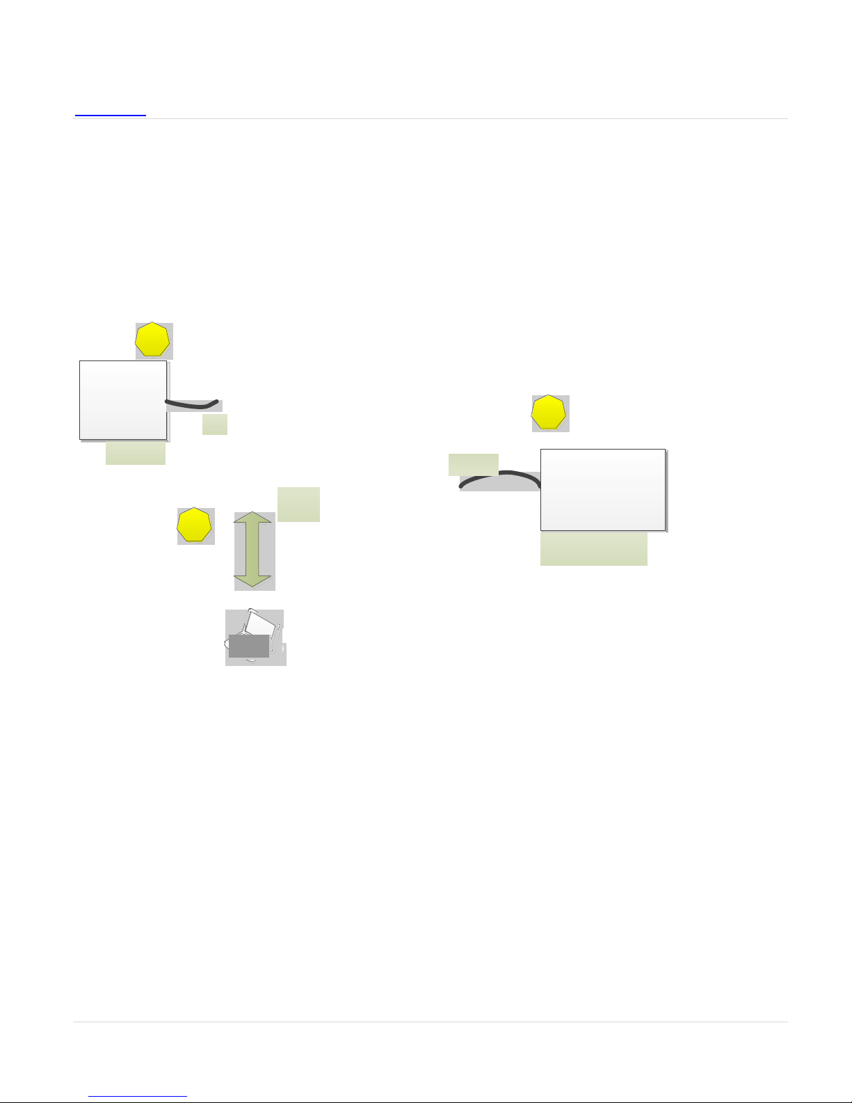
Basic Operation
1) Connect a low noise 3.3 V power supply to the Vcc connector lo cated at the top left of the b oard.
2) Connect 122.88 MHz signal from signal gene rator output to CLKin 0 of board.
3) Please see Appendix B for quick start on interfacing the board. Co nnect PC to the uWire header.
1
Power
Supply
Vcc
2
3.3V
3
Pleasesee
Pleasesee
AppendixBfor
AppendixBfor
interfaceinfo
interfaceinfo
LaptoporPC
LaptoporPC
4) Start CodeLoader4.exe
uWire
header
CLKin0
SMACable
SMACable
SignalGenerator
122.88Mhz
November 2013 LMK01000 Evaluation Board SNAU037A 5
Copyright © 2013, Texas Instruments Incorporated
Page 6

5) Select the device by ”Select Device” “Clock Conditioners”
www.ti.com
6) Enable the output to measure (example CLKout0 is ena bled below)
6 SNAU037A LMK01000 Evaluation Board November 2013
Copyright © 2013, Texas Instruments Incorporated
Page 7

www.ti.com
7) Program the part by clicking “Keyboard Controls” “Load Device” or by pressing Ctrl+L.
***
Be advised: GOE and SYNC* on the IC have internal pull-ups. Voltage dividers are used to
lower 5 V LPT ports to safe levels for the device while still programming with 3.3 V LPT ports.
When the cable is removed however, the pull-down of the voltage divider will overpower the
pullup of the GOE or SYNC*. For this reason GOE is disconnected so the cable can be
disconnected and the outputs still will be on. However, or any channels which have dividers
enabled, the SYNC* will go low and cause them to stop oscillating. Future versions of the
evaluation board have zener diodes on GOE and SYNC* to eliminate this issue.
November 2013 LMK01000 Evaluation Board SNAU037A 7
Copyright © 2013, Texas Instruments Incorporated
Page 8

8 SNAU037A LMK01000 Evaluation Board November 2013
Copyright © 2013, Texas Instruments Incorporated
Appendix A: Schematics
LMK02000 - Main Board
LMK02000 - Main Board.sch
LMK02000 - Outputs
LMK02000 - Outputs.sch
F1
SMA _CONN
1 2
3 4
5 6
7 8
9 10
GND_J 1
HEAD ER_2X5
1 2
3 4
5 6
7 8
9 10
VCC_ J 1
HEAD ER_2X5
Vcc Vcc
1 2
3 4
5 6
7 8
9 10
GND_J 2
HEAD ER_2X5
1 2
3 4
5 6
7 8
9 10
VCC_ J 2
HEAD ER_2X5
Vcc Vcc
Page 9

www.ti.com
November 2013 LMK01000 Evaluation Board SNAU037A 9
Copyright © 2013, Texas Instruments Incorporated
CLK out 4
SMA
CLK out 4*
SMA
R121
Open
R114
Open
R128
Open
R113
Open
R127
Open
C92
0.1 uF
C96
0.1 uF
R126
120 ohm
R125
120 ohm
CLKout4*
CLKout4
Vcc Vcc
CLK out 0
SMA
CLK out 0*
SMA
R93
Open
R86
Open
R100
Open
R85
Open
R99
Open
C84
0.1 uF
C88
0.1 uF
R98
Open
R97
Open
CLKout0*
CLKout0
Vcc Vcc
CLKout5
Open
CLK out 5*
Open
R122
Open
R116
Open
R132
Open
R115
Open
R131
Open
C93
0.1 uF
C97
0.1 uF
R130
120 ohm
R129
120 ohm
CLK out 5*
CLK out5
Vcc Vcc
CLKout1
Open
CLK out 1*
Open
R94
Open
R88
Open
R104
Open
R87
Open
R103
Open
C85
0.1 uF
C89
0.1 uF
R102
Open
R101
Open
CLK out 1*
CLK out1
Vcc Vcc
CLK out6
Open
CLK out6 *
Open
R123
Open
R118
Open
R136
Open
R117
Open
R135
Open
C94
0.1 uF
C98
0.1 uF
R134
120 ohm
R133
120 ohm
CLKout6*
CLKout6
Vcc Vcc
CLK out2
Open
CLK out2*
Open
R95
Open
R90
Open
R108
Open
R89
Open
R107
Open
C86
0.1 uF
C90
0.1 uF
R106
Open
R105
Open
CLKout2*
CLKout2
Vcc Vcc
CLK out7
SMA
CLK out7 *
SMA
R124
Open
R120
Open
R140
Open
R119
Open
R139
Open
C95
0.1 uF
C99
0.1 uF
R138
120 ohm
R137
120 ohm
CLK out 7*
CLK out 7
Vcc Vcc
CLK out3
SMA
CLK out3 *
SMA
R96
Open
R92
Open
R112
Open
R91
Open
R111
Open
C87
0.1 uF
C91
0.1 uF
R110
120 ohm
R109
120 ohm
CLK out 3*
CLK out 3
Vcc Vcc
CLKout0 CLKout1 CLKout2 CLKout3
CLKout4 CLKout5 CLKout6 CLKout7
PC4
PC0 PC1 PC2 PC3
PC5 PC6 PC7
PC0b
PC4b PC5b PC6b PC7b
PC3bPC2bPC1b
Page 10

www.ti.com
10 SNAU037A LMK01000 Evaluation Board November 2013
Copyright © 2013, Texas Instruments Incorporated
C1
390 pF
C2
Open
C80
10 uF
Vcc
SMA
C14
10 uF
C70
1 uF
Vcc3
R5
0 ohm
Vcc
Vcc4
Vcc7
Vcc8
C78
47 pF
R65
270 ohm
R64
270 ohm
R62
18 ohms
R68
0 ohm
1 2
3 4
5 6
7 8
9 10
uWire
HEADER_2X5
R59
15 k
R75
Open
R58
27 k
R56
27 k
R55
15 k
R54
27 k
R2
4.7 k
R57
15 k
Vcc10
C59
0.1 uF
C13
100 pF
C16
100 pF
C60
1 uF
C61
0.1 uF
C71
1 uF
Vcc5
Vcc6
C62
0.1 uF
C18
100 pF
C22
100 pF
C63
1 uF
C64
0.1 uF
C72
1 uF
Vcc11
Vcc12
C65
0.1 uF
C25
100 pF
C29
100 pF
C66
1 uF
C67
0.1 uF
C58
1 uF
Vcc13
Vcc14
C54
0.1 uF
C33
100 pF
C38
100 pF
C68
1 uF
C69
0.1 uF
C55
1 uF
Vcc1
Vcc2
C45
0.1 uF
C20
100 pF
C23
100 pF
C46
1 uF
C47
0.1 uF
C56
1 uF
Vcc7
Vcc8
C48
0.1 uF
C28
100 pF
C32
100 pF
C49
1 uF
C50
0.1 uF
C57
1 uF
Vcc9
Vcc10
C51
0.1 uF
C36
100 pF
C42
100 pF
C52
1 uF
C53
0.1 uF
Vcc3 Vcc4 Vcc5 Vcc6
Vcc11Vcc12Vcc13Vcc14
Vcc1
Vcc2
Vcc
Vcc9
R76
Open
LD_TP
C81
0.1 uF
Fin
SMA
Vt
1
G
2
Vcc
3
G
4
Fout
5
G
6
NC
7
G
8
Y4
Open
Fout
SMA
CLKout 7*
CLKout7
CLKout6
CLKout6*
CLKout 4
CLKout 4 *
CLKout5
CLKout5*
CLKout0
CLKout 0 *
CLKout1
CLKout1*
CLKout2*
CLKout2
CLKout3*
CLKout3
LD
GOE
GOE
GND
0
GND
1
NC
2
Vcc1
3
CLKuWire
4
DATAuWire
5
LEuWire
6
NC
7
Vcc2
8
LDObyp 1
9
LDObyp 2
10
GOE
11
NC
12
Vcc313CLKout014CLKout0*15Vcc416CLKout117CLKout1*18Vcc519CLKout220CLKout2*21Vcc622CLKout323CLKout3*
24
GND
25
Vcc7
26
SYNC*
27
CLKin0
28
CLKi n0*
29
Vcc8
30
Vcc9
31
NC
32
Vcc10
33
CLKin1
34
CLKi n1*
35
Bias
36
Vcc11
37
CLKout4
38
CLKout4*
39
Vcc12
40
CLKout5
41
CLKout5*
42
Vcc13
43
CLKout6
44
CLKout6*
45
Vcc14
46
CLKout7
47
CLKout7*
48
U1
LMK01000
CLKuWire
DATAuWire
LEuWire
LEuWireDATAuWireCLKuWire
Fin*
SMA
Vcc
R63
0 ohm
Vtune VCXO
R26
Open
Vtune VCO
Vcc
R30
0 ohm
C30
Open
C31
0.1 uF
DUT_Fin
DUT_Fin *
DUT_Fin
DUT_Fin *
DUT_OSCin *
DUT_OSCin
R47
0 ohm
R48
0 ohm
R38
Open
R39
Open
C34
0.1 uF
C40
0.1 uF
R33
0 ohm
R46
0 ohm
R78
0 ohm
R77
0 ohm
C73
1 uF
OSCin
SMA
OSCin*
SMA
DUT_OSCin
DUT_OSCin *
OSC_RF
R16
0 ohm
R20
0 ohm
R12
0 ohm
R19
Open
C6
0.1 uF
C9
0.1 uF
R15
0 ohm
R25
0 ohm
C44
Open
C10
Open
R49
0 ohm
R51
Open
C21
10 uF
C17
10 uF
Vtune
Open
R79
Open
Fout*
Open
R53
0 ohm
C77
Open
C79
Open
R84
27 k
R82
15 k
SYNC*
C83
100 pF
SYNC*
R71
Open
GOE
Open
SYNC*
Open
Vcc
R81
Open
Vcc
C75
Open
C76
Open
LD
R61
Open
C74
Open
R52
0 ohm
LD
Open
R60
15 k
R50
Open
Vcc
C3
Open
Vin
Vin
R24
0 ohm
VCXO
VCO
Fin
OSCin
R18
Open
Vcc
OSC_RF1
R14
0 ohm
C7
OpenC80.1 uF
OSC
Out3GND
2
Vcont1Vcc
4
Y2
CC33xx
R21
Open
C39
Open
C19
Open
C12
Open
C2_AUX
0.1 uF
C1_AUX
3.3 nF
C82
Open
R80
Open
R2_AUX
47 k
R72
Open
R73
Open
R69
0 ohm
C2p_AUX
Open
C2p
10 uF
C26
Open
C27
Open
R28
Open
R70
Open
C43
Open
Vtune VCXO Vtun eVCO
R66
Open
R74
Open
R83
Open
GOE_TP
SYNC*_ TP
C15
10 uF
VCO_VCXO_ Vcc
Open
OSC_Vcc
Open
R1
Open
R29
Open
R27
Open
R34
Open
R35
Open
C37 Open
C41 Open
Pin10_TP
Pin7_TP
Pin5_TP
VccPlan e
GND_tp1
Vcc
Vcc
Vcc
C35
Open
GND_tp 2
R32
Open
R45
51 ohm
R31
Open
R44
51 ohm
Vcc Vcc
CLKuWire
DATAuWire LEuWire
TC1-1-13M+
R10
Open
R11
Open
R23
51 ohm
R22
51 ohm
Vcc Vc c
P
1
NC
2
PD3S
4
SCT
5
SD
6
ADT2-1 T
B1
BALUN - ADT2-1 T
P
1
NC
2
PD3S
4
SCT
5
SD
6
BALUN
B2
BALUN - ADT-ETC Hy brid
P
1
NC
2
PD3S
4
SCT
5
SD
6
BALUN
B3
BALUN - ADT-ETC Hyb rid
R67
Open
GND
Vtune
1
NC
2
GND3RF
4
RF*
5
Vs
6
Y3
VCXO
R40
0 ohm
R41
0 ohm
R42
Open
R43
Open
R37
Open
R36
Open
GND GND
GNDGND
C24
Open
GND
R4
22 ohm
R6
220 ohmR7220 ohm
GNDGND
OSC_RF2
Vtune
1
NC
2
GND3RF
4
RF*
5
Vs
6
Y1
CCHD0950
R9
Open
R3
0 ohm
R8
Open
OSC_RF1
OSC_RF2
R17
Open
C11
Open
Vcc
Vcc
R13
Open
C4
OpenC5Open
VCXO_VCO_ Vcc
VCXO_RF
VCXO_RF*
VCO_RF
R142
Open
GND
R141
Open
GND
Page 11

Appendix B: Quick Start for EVM Communications
Codeloader is the software used to communicate with the EVM (Please download the latest version from TI.com -
http://www.ti.com/tool/codeloader). This EVM can be controlled through the uWire interface on board. There are two options
in communicating with the uWire interface from the computer.
OPTION 1
Open Codeloader. exe Click “Select Device” Click “Port Setup” tab Click “LPT” (in Communication Mode)
OPTION 2
November 2013 LMK01000 Evaluation Board SNAU037A 11
Copyright © 2013, Texas Instruments Incorporated
Page 12

The Adapter Board
This table describes the pins configuration on the adapter board for each EVM board (See examples below table)
EVM
LMX2581 A4 B1 C2 E5 F1 G1 H1 BUFEN (pin 1), Trigger (pin 7)
LMX2541 A4 C3 E4 F1 G1 H1 CE (pin 1), Trigger (pin 10)
LMK0400x A0 C3 E5 F1 G1 H1 GOE (pin 7)
LMK01000 A0 C1 E5 F1 G1 H1 GOE (pin 7)
LMK030xx A0 C1 E5 F1 G1 H1 SYNC (pin 7)
LMK02000 A0 C1 E5 F1 G1 H1 SYNC (pin 7)
LMK0480x A0 B2 C3 E5 F0 G0 H1 Status_CLKin1 (pin 3)
LMK04816/4906 A0 B2 C3 E5 F0 G0 H1 Status_CLKin1 (pin 3)
LMK01801 A0 B4 C5 E2 F0 G0 H1 Test (pin 3), SYNC0 (pin 10)
LMK0482x (prelease) A0 B5 C3 D2 E4 F0 G0 H1 CLKin1_SEL (pin 6), Reset (pin 10)
LMX2531 A0 E5 F2 G1 H2 Trigger (pin 1)
LMX2485/7 A0 C1 E5 F2 G1 H0 ENOSC (pin 7), CE (pin 10)
LMK03200 A0 E5 F0 G0 H1 SYNC (pin 7)
LMK03806 A0 C1 E5 F0 G0 H1
LMK04100 A0 C1 E5 F1 G1 H1
Example adapter configuration (LMK01801)
A B C D E F G H
Jumper Bank Code Loader Configuration
www.ti.com
Open Codeloader. exe Click “Select Device” Click “Port Setup” Tab Click “USB” (in Communication Mode)
*Remember to also make modifications in “Pin Configuration” Section according to Table above.
12 SNAU037A LMK01000 Evaluation Board November 2013
Copyright © 2013, Texas Instruments Incorporated
Page 13

EVALUATION BOARD/KIT/MODULE (EVM) ADDITIONAL TERMS
Texas Instruments (TI) provides the enclosed Evaluation Board/Kit/Module (EVM) under the following conditions:
The user assumes all responsibility and liability for proper and safe handling of the goods. Further, the user indemnifies TI from all claims
arising from the handling or use of the goods.
Should this evaluation board/kit not meet the specifications indicated in the User’s Guide, the board/kit may be returned within 30 days from
the date of delivery for a full refund. THE FOREGOING LIMITED WARRANTY IS THE EXCLUSIVE WARRANTY MADE BY SELLER TO
BUYER AND IS IN LIEU OF ALL OTHER WARRANTIES, EXPRESSED, IMPLIED, OR STATUTORY, INCLUDING ANY WARRANTY OF
MERCHANTABILITY OR FITNESS FOR ANY PARTICULAR PURPOSE. EXCEPT TO THE EXTENT OF THE INDEMNITY SET FORTH
ABOVE, NEITHER PARTY SHALL BE LIABLE TO THE OTHER FOR ANY INDIRECT, SPECIAL, INCIDENTAL, OR CONSEQUENTIAL
DAMAGES.
Please read the User's Guide and, specifically, the Warnings and Restrictions notice in the User's Guide prior to handling the product. This
notice contains important safety information about temperatures and voltages. For additional information on TI's environmental and/or safety
programs, please visit www.ti.com/esh or contact TI.
No license is granted under any patent right or other intellectual property right of TI covering or relating to any machine, process, or
combination in which such TI products or services might be or are used. TI currently deals with a variety of customers for products, and
therefore our arrangement with the user is not exclusive. TI assumes no liability for applications assistance, customer product design,
software performance, or infringement of patents or services described herein.
REGULATORY COMPLIANCE INFORMATION
As noted in the EVM User’s Guide and/or EVM itself, this EVM and/or accompanying hardware may or may not be subject to the Federal
Communications Commission (FCC) and Industry Canada (IC) rules.
For EVMs not subject to the above rules, this evaluation board/kit/module is intended for use for ENGINEERING DEVELOPMENT,
DEMONSTRATION OR EVALUATION PURPOSES ONLY and is not considered by TI to be a finished end product fit for general consumer
use. It generates, uses, and can radiate radio frequency energy and has not been tested for compliance with the limits of computing
devices pursuant to part 15 of FCC or ICES-003 rules, which are designed to provide reasonable protection against radio frequency
interference. Operation of the equipment may cause interference with radio communications, in which case the user at his own expense will
be required to take whatever measures may be required to correct this interference.
General Statement for EVMs including a radio
User Power/Frequency Use Obligations: This radio is intended for development/professional use only in legally allocated frequency and
power limits. Any use of radio frequencies and/or power availability of this EVM and its development application(s) must comply with local
laws governing radio spectrum allocation and power limits for this evaluation module. It is the user’s sole responsibility to only operate this
radio in legally acceptable frequency space and within legally mandated power limitations. Any exceptions to this are strictly prohibited and
unauthorized by Texas Instruments unless user has obtained appropriate experimental/development licenses from local regulatory
authorities, which is responsibility of user including its acceptable authorization.
For EVMs annotated as FCC – FEDERAL COMMUNICATIONS COMMISSION Part 15 Compliant
Caution
This device complies with part 15 of the FCC Rules. Operation is subject to the following two conditions: (1) This device may not cause
harmful interference, and (2) this device must accept any interference received, including interference that may cause undesired operation.
Changes or modifications not expressly approved by the party responsible for compliance could void the user's authority to operate the
equipment.
FCC Interference Statement for Class A EVM devices
This equipment has been tested and found to comply with the limits for a Class A digital device, pursuant to part 15 of the FCC Rules.
These limits are designed to provide reasonable protection against harmful interference when the equipment is operated in a commercial
environment. This equipment generates, uses, and can radiate radio frequency energy and, if not installed and used in accordance with the
instruction manual, may cause harmful interference to radio communications. Operation of this equipment in a residential area is likely to
cause harmful interference in which case the user will be required to correct the interference at his own expense.
Page 14

FCC Interference Statement for Class B EVM devices
This equipment has been tested and found to comply with the limits for a Class B digital device, pursuant to part 15 of the FCC Rules.
These limits are designed to provide reasonable protection against harmful interference in a residential installation. This equipment
generates, uses and can radiate radio frequency energy and, if not installed and used in accordance with the instructions, may cause
harmful interference to radio communications. However, there is no guarantee that interference will not occur in a particular installation. If
this equipment does cause harmful interference to radio or television reception, which can be determined by turning the equipment off and
on, the user is encouraged to try to correct the interference by one or more of the following measures:
• Reorient or relocate the receiving antenna.
• Increase the separation between the equipment and receiver.
• Connect the equipment into an outlet on a circuit different from that to which the receiver is connected.
• Consult the dealer or an experienced radio/TV technician for help.
For EVMs annotated as IC – INDUSTRY CANADA Compliant
This Class A or B digital apparatus complies with Canadian ICES-003.
Changes or modifications not expressly approved by the party responsible for compliance could void the user’s authority to operate the
equipment.
Concerning EVMs including radio transmitters
This device complies with Industry Canada licence-exempt RSS standard(s). Operation is subject to the following two conditions: (1) this
device may not cause interference, and (2) this device must accept any interference, including interference that may cause undesired
operation of the device.
Concerning EVMs including detachable antennas
Under Industry Canada regulations, this radio transmitter may only operate using an antenna of a type and maximum (or lesser) gain
approved for the transmitter by Industry Canada. To reduce potential radio interference to other users, the antenna type and its gain should
be so chosen that the equivalent isotropically radiated power (e.i.r.p.) is not more than that necessary for successful communication.
This radio transmitter has been approved by Industry Canada to operate with the antenna types listed in the user guide with the maximum
permissible gain and required antenna impedance for each antenna type indicated. Antenna types not included in this list, having a gain
greater than the maximum gain indicated for that type, are strictly prohibited for use with this device.
Cet appareil numérique de la classe A ou B est conforme à la norme NMB-003 du Canada.
Les changements ou les modifications pas expressément approuvés par la partie responsable de la conformité ont pu vider l’autorité de
l'utilisateur pour actionner l'équipement.
Concernant les EVMs avec appareils radio
Le présent appareil est conforme aux CNR d'Industrie Canada applicables aux appareils radio exempts de licence. L'exploitation est
autorisée aux deux conditions suivantes : (1) l'appareil ne doit pas produire de brouillage, et (2) l'utilisateur de l'appareil doit accepter tout
brouillage radioélectrique subi, même si le brouillage est susceptible d'en compromettre le fonctionnement.
Concernant les EVMs avec antennes détachables
Conformément à la réglementation d'Industrie Canada, le présent émetteur radio peut fonctionner avec une antenne d'un type et d'un gain
maximal (ou inférieur) approuvé pour l'émetteur par Industrie Canada. Dans le but de réduire les risques de brouillage radioélectrique à
l'intention des autres utilisateurs, il faut choisir le type d'antenne et son gain de sorte que la puissance isotrope rayonnée équivalente
(p.i.r.e.) ne dépasse pas l'intensité nécessaire à l'établissement d'une communication satisfaisante.
Le présent émetteur radio a été approuvé par Industrie Canada pour fonctionner avec les types d'antenne énumérés dans le manuel
d’usage et ayant un gain admissible maximal et l'impédance requise pour chaque type d'antenne. Les types d'antenne non inclus dans
cette liste, ou dont le gain est supérieur au gain maximal indiqué, sont strictement interdits pour l'exploitation de l'émetteur.
SPACER
SPACER
SPACER
SPACER
SPACER
SPACER
SPACER
SPACER
Page 15

【【Important Notice for Users of EVMs for RF Products in Japan】】
This development kit is NOT certified as Confirming to Technical Regulations of Radio Law of Japan
If you use this product in Japan, you are required by Radio Law of Japan to follow the instructions below with respect to this product:
1. Use this product in a shielded room or any other test facility as defined in the notification #173 issued by Ministry of Internal Affairs and
Communications on March 28, 2006, based on Sub-section 1.1 of Article 6 of the Ministry’s Rule for Enforcement of Radio Law of
Japan,
2. Use this product only after you obtained the license of Test Radio Station as provided in Radio Law of Japan with respect to this
product, or
3. Use of this product only after you obtained the Technical Regulations Conformity Certification as provided in Radio Law of Japan with
respect to this product. Also, please do not transfer this product, unless you give the same notice above to the transferee. Please note
that if you could not follow the instructions above, you will be subject to penalties of Radio Law of Japan.
(address) 24-1, Nishi-Shinjuku 6 chome, Shinjuku-ku, Tokyo, Japan
http://www.tij.co.jp
【無線電波を送信する製品の開発キットをお使いになる際の注意事項】
本開発キットは技術基準適合証明を受けておりません。
本製品のご使用に際しては、電波法遵守のため、以下のいずれかの措置を取っていただく必要がありますのでご注意ください。
1. 電波法施行規則第6条第1項第1号に基づく平成18年3月28日総務省告示第173号で定められた電波暗室等の試験設備でご使用いただく。
2. 実験局の免許を取得後ご使用いただく。
3. 技術基準適合証明を取得後ご使用いただく。
なお、本製品は、上記の「ご使用にあたっての注意」を譲渡先、移転先に通知しない限り、譲渡、移転できないものとします。
上記を遵守頂けない場合は、電波法の罰則が適用される可能性があることをご留意ください。
日本テキサス・インスツルメンツ株式会社
東京都新宿区西新宿6丁目24番1号
西新宿三井ビル
http://www.tij.co.jp
Texas Instruments Japan Limited
SPACER
SPACER
SPACER
SPACER
SPACER
SPACER
SPACER
SPACER
SPACER
SPACER
SPACER
SPACER
SPACER
SPACER
SPACER
SPACER
SPACER
Page 16

EVALUATION BOARD/KIT/MODULE (EVM)
WARNINGS, RESTRICTIONS AND DISCLAIMERS
For Feasibility Evaluation Only, in Laboratory/Development Environments. Unless otherwise indicated, this EVM is not a finished
electrical equipment and not intended for consumer use. It is intended solely for use for preliminary feasibility evaluation in
laboratory/development environments by technically qualified electronics experts who are familiar with the dangers and application risks
associated with handling electrical mechanical components, systems and subsystems. It should not be used as all or part of a finished end
product.
Your Sole Responsibility and Risk. You acknowledge, represent and agree that:
1. You have unique knowledge concerning Federal, State and local regulatory requirements (including but not limited to Food and Drug
Administration regulations, if applicable) which relate to your products and which relate to your use (and/or that of your employees,
affiliates, contractors or designees) of the EVM for evaluation, testing and other purposes.
2. You have full and exclusive responsibility to assure the safety and compliance of your products with all such laws and other applicable
regulatory requirements, and also to assure the safety of any activities to be conducted by you and/or your employees, affiliates,
contractors or designees, using the EVM. Further, you are responsible to assure that any interfaces (electronic and/or mechanical)
between the EVM and any human body are designed with suitable isolation and means to safely limit accessible leakage currents to
minimize the risk of electrical shock hazard.
3. Since the EVM is not a completed product, it may not meet all applicable regulatory and safety compliance standards (such as UL,
CSA, VDE, CE, RoHS and WEEE) which may normally be associated with similar items. You assume full responsibility to determine
and/or assure compliance with any such standards and related certifications as may be applicable. You will employ reasonable
safeguards to ensure that your use of the EVM will not result in any property damage, injury or death, even if the EVM should fail to
perform as described or expected.
4. You will take care of proper disposal and recycling of the EVM’s electronic components and packing materials.
Certain Instructions. It is important to operate this EVM within TI’s recommended specifications and environmental considerations per the
user guidelines. Exceeding the specified EVM ratings (including but not limited to input and output voltage, current, power, and
environmental ranges) may cause property damage, personal injury or death. If there are questions concerning these ratings please contact
a TI field representative prior to connecting interface electronics including input power and intended loads. Any loads applied outside of the
specified output range may result in unintended and/or inaccurate operation and/or possible permanent damage to the EVM and/or
interface electronics. Please consult the EVM User's Guide prior to connecting any load to the EVM output. If there is uncertainty as to the
load specification, please contact a TI field representative. During normal operation, some circuit components may have case temperatures
greater than 60°C as long as the input and output are maintained at a normal ambient operating temperature. These components include
but are not limited to linear regulators, switching transistors, pass transistors, and current sense resistors which can be identified using the
EVM schematic located in the EVM User's Guide. When placing measurement probes near these devices during normal operation, please
be aware that these devices may be very warm to the touch. As with all electronic evaluation tools, only qualified personnel knowledgeable
in electronic measurement and diagnostics normally found in development environments should use these EVMs.
Agreement to Defend, Indemnify and Hold Harmless. You agree to defend, indemnify and hold TI, its licensors and their representatives
harmless from and against any and all claims, damages, losses, expenses, costs and liabilities (collectively, "Claims") arising out of or in
connection with any use of the EVM that is not in accordance with the terms of the agreement. This obligation shall apply whether Claims
arise under law of tort or contract or any other legal theory, and even if the EVM fails to perform as described or expected.
Safety-Critical or Life-Critical Applications. If you intend to evaluate the components for possible use in safety critical applications (such
as life support) where a failure of the TI product would reasonably be expected to cause severe personal injury or death, such as devices
which are classified as FDA Class III or similar classification, then you must specifically notify TI of such intent and enter into a separate
Assurance and Indemnity Agreement.
Mailing Address: Texas Instruments, Post Office Box 655303, Dallas, Texas 75265
Copyright © 2013, Texas Instruments Incorporated
Page 17

IMPORTANT NOTICE
Texas Instruments Incorporated and its subsidiaries (TI) reserve the right to make corrections, enhancements, improvements and other
changes to its semiconductor products and services per JESD46, latest issue, and to discontinue any product or service per JESD48, latest
issue. Buyers should obtain the latest relevant information before placing orders and should verify that such information is current and
complete. All semiconductor products (also referred to herein as “components”) are sold subject to TI’s terms and conditions of sale
supplied at the time of order acknowledgment.
TI warrants performance of its components to the specifications applicable at the time of sale, in accordance with the warranty in TI’s terms
and conditions of sale of semiconductor products. Testing and other quality control techniques are used to the extent TI deems necessary
to support this warranty. Except where mandated by applicable law, testing of all parameters of each component is not necessarily
performed.
TI assumes no liability for applications assistance or the design of Buyers’ products. Buyers are responsible for their products and
applications using TI components. To minimize the risks associated with Buyers’ products and applications, Buyers should provide
adequate design and operating safeguards.
TI does not warrant or represent that any license, either express or implied, is granted under any patent right, copyright, mask work right, or
other intellectual property right relating to any combination, machine, or process in which TI components or services are used. Information
published by TI regarding third-party products or services does not constitute a license to use such products or services or a warranty or
endorsement thereof. Use of such information may require a license from a third party under the patents or other intellectual property of the
third party, or a license from TI under the patents or other intellectual property of TI.
Reproduction of significant portions of TI information in TI data books or data sheets is permissible only if reproduction is without alteration
and is accompanied by all associated warranties, conditions, limitations, and notices. TI is not responsible or liable for such altered
documentation. Information of third parties may be subject to additional restrictions.
Resale of TI components or services with statements different from or beyond the parameters stated by TI for that component or service
voids all express and any implied warranties for the associated TI component or service and is an unfair and deceptive business practice.
TI is not responsible or liable for any such statements.
Buyer acknowledges and agrees that it is solely responsible for compliance with all legal, regulatory and safety-related requirements
concerning its products, and any use of TI components in its applications, notwithstanding any applications-related information or support
that may be provided by TI. Buyer represents and agrees that it has all the necessary expertise to create and implement safeguards which
anticipate dangerous consequences of failures, monitor failures and their consequences, lessen the likelihood of failures that might cause
harm and take appropriate remedial actions. Buyer will fully indemnify TI and its representatives against any damages arising out of the use
of any TI components in safety-critical applications.
In some cases, TI components may be promoted specifically to facilitate safety-related applications. With such components, TI’s goal is to
help enable customers to design and create their own end-product solutions that meet applicable functional safety standards and
requirements. Nonetheless, such components are subject to these terms.
No TI components are authorized for use in FDA Class III (or similar life-critical medical equipment) unless authorized officers of the parties
have executed a special agreement specifically governing such use.
Only those TI components which TI has specifically designated as military grade or “enhanced plastic” are designed and intended for use in
military/aerospace applications or environments. Buyer acknowledges and agrees that any military or aerospace use of TI components
which have not been so designated is solely at the Buyer's risk, and that Buyer is solely responsible for compliance with all legal and
regulatory requirements in connection with such use.
TI has specifically designated certain components as meeting ISO/TS16949 requirements, mainly for automotive use. In any case of use of
non-designated products, TI will not be responsible for any failure to meet ISO/TS16949.
Products Applications
Audio www.ti.com/audio Automotive and Transportation www.ti.com/automotive
Amplifiers amplifier.ti.com Communications and Telecom www.ti.com/communications
Data Converters dataconverter.ti.com Computers and Peripherals www.ti.com/computers
DLP® Products www.dlp.com Consumer Electronics www.ti.com/consumer-apps
DSP dsp.ti.com Energy and Lighting www.ti.com/energy
Clocks and Timers www.ti.com/clocks Industrial www.ti.com/industrial
Interface interface.ti.com Medical www.ti.com/medical
Logic logic.ti.com Security www.ti.com/security
Power Mgmt power.ti.com Space, Avionics and Defense www.ti.com/space-avionics-defense
Microcontrollers microcontroller.ti.com Video and Imaging www.ti.com/video
RFID www.ti-rfid.com
OMAP Applications Processors www.ti.com/omap TI E2E Community e2e.ti.com
Wireless Connectivity www.ti.com/wirelessconnectivity
Mailing Address: Texas Instruments, Post Office Box 655303, Dallas, Texas 75265
Copyright © 2013, Texas Instruments Incorporated
 Loading...