

Page 1

User's Guide
SLOU454–June 2016
LMH2832EVM-50 Evaluation Module
The LMH2832EVM-50 evaluation module (EVM) is used to evaluate the dual LMH2832, digitally-controlled
variable gain amplifier (DVGA) in a 40-pin VQFN package. The EVM is used to easily demonstrate the
functionality and performance of LMH2832 across all the gain settings in a 50-Ω input environment. The
EVM is ready to connect to power supplies, signal source, USB, and test instruments through the use of
onboard connectors. By default, the LMH2832EVM powers up to the 10-dB gain setting with the board
supporting only single-supply operation. A USB connector on the EVM facilitates programming of the
DVGA gain registers using an FTDI USB-to-SPI bus translator chip.
spacer
Contents
1 Features....................................................................................................................... 2
2 EVM Specifications.......................................................................................................... 3
3 Evaluation Board Setup Block Diagram .................................................................................. 3
4 Setup Procedure............................................................................................................. 4
4.1 Connect EVM to a 5-V Bench Power Supply ................................................................... 4
4.2 Connect EVM to the External Signal Source at the Input ..................................................... 4
4.3 Connect EVM to the External Test Equipment at the Output................................................. 4
4.4 PD (Power Down) Input............................................................................................ 4
4.5 Connect EVM to the PC and LMH2832 EVM GUI Installation................................................ 5
5 Amplifier Device Register Configuration .................................................................................. 5
5.1 LMH2832 EVM GUI ................................................................................................ 6
5.2 Low Level View ..................................................................................................... 7
6 Evaluation Troubleshooting................................................................................................. 8
7 LMH2832 EVM Schematic, Layer Prints, and Bill of Materials ........................................................ 9
7.1 Schematic............................................................................................................ 9
7.2 Layer Prints ........................................................................................................ 11
7.3 Bill of Materials .................................................................................................... 19
1 LMH2832EVM Board........................................................................................................ 2
2 LMH2832 Evaluation Board Setup Block Diagram...................................................................... 3
3 LMH2832 EVM GUI Front Page ........................................................................................... 6
4 Low Level View Tab......................................................................................................... 7
5 Schematic - Analog.......................................................................................................... 9
6 Schematic - Digital ......................................................................................................... 10
7 Top Layer ................................................................................................................... 11
8 Layer 2 Ground Plane ..................................................................................................... 12
9 Layer 3 GND Plane ........................................................................................................ 13
10 Layer 4 GND Plane ........................................................................................................ 14
11 Layer 5 V+ Plane........................................................................................................... 15
12 Layer 6 Ground Plane ..................................................................................................... 16
13 Layer 7 GND Plane ........................................................................................................ 17
14 Bottom Layer................................................................................................................ 18
SLOU454–June 2016
Submit Documentation Feedback
List of Figures
List of Tables
Copyright © 2016, Texas Instruments Incorporated
LMH2832EVM-50 Evaluation Module
1
Page 2

Features
1 EVM Specifications.......................................................................................................... 3
2 LMH2832 Default SPI Register Map ...................................................................................... 5
3 LMH2832 GUI Tab Descriptions........................................................................................... 6
4 Low Level View Controls ................................................................................................... 7
5 LMH2832EVM Bill of Materials........................................................................................... 19
1 Features
The key features of this EVM include:
• Configured for 5-V single-supply operation
• Designed for AC-coupled, single-ended, 50-Ω input, and output connection
• Interface to the inputs and outputs using SMA connectors
• USB connector and FTDI USB-to-SPI bus translator chip to successfully program the DVGA gain
registers
Figure 1 shows the LMH2832EVM board.
www.ti.com
2
LMH2832EVM-50 Evaluation Module
Figure 1. LMH2832EVM Board
Copyright © 2016, Texas Instruments Incorporated
Submit Documentation Feedback
SLOU454–June 2016
Page 3

USB
½ LMH2832
5-V Bench
Power Supply
5 V GND
40 Q
40 Q
SPI
LMH2832 EVM
Low-Noise
Signal Generator
Spectrum Analyzer
(V+)
Band-Pass
Filter
0.1 µF
0.1 µF
ETC1-1-13T
(1:1, Zo = 50 Ÿ)
MABA011038
(1:3, Zo = 50 Ÿ)
0.1 µF
0.1 µF
SMA
SMA
www.ti.com
2 EVM Specifications
Table 1 lists the EVM specifications.
Table 1. EVM Specifications
Parameter Value
V
Single-supply voltage range (V– = Ground) 4.5 V to 5.25 V
s
GND Ground reference pins Tied to GND or 0 V
PDA
or
Power down (PD) input voltage GND to V
PDB
I
Supply current with both channels enabled approximately 204 mA
s
I
Input voltage Vs±, Max
IN
3 Evaluation Board Setup Block Diagram
The following sections help in setting up the LMH2832 evaluation board hardware and software required
to program the internal registers of the LMH2832.
Figure 2 illustrates the LMH2832 evaluation board setup block diagram.
EVM Specifications
s
Figure 2. LMH2832 Evaluation Board Setup Block Diagram
SLOU454–June 2016
Submit Documentation Feedback
Copyright © 2016, Texas Instruments Incorporated
LMH2832EVM-50 Evaluation Module
3
Page 4

Setup Procedure
4 Setup Procedure
This section describes the hardware setup procedure and the installation of the software to program the
LMH2832 registers.
4.1 Connect EVM to a 5-V Bench Power Supply
1. Before making connections from the bench power supply to the evaluation board supply pin connector,
set the bench power supply to 5 V, and switch the bench power supply OFF.
2. While the supplies are turned OFF, connect the evaluation board power supply pins (V+ and GND) to
the bench power supply of 5 V and GND, as shown in Figure 2, using a low-noise bench power supply.
3. Turn ON the bench supplies after the power supply connections have been made. The LMH2832
evaluation board should read an approximate DC current of 204 mA for 5-V single supply with both the
LMH2832 channels enabled. Input and output pins should be biased to the mid-supplies as specified in
the LMH2832 data sheet (SBOS709) for proper operation.
4.2 Connect EVM to the External Signal Source at the Input
1. The LMH2832EVM-50 evaluation board provides the customer flexibility in testing at different input
frequencies using on-board input and output baluns as shown in Figure 2.
2. It is recommended to use 6-dB attenuator pads at the input while connecting a 50-Ω signal source to
the LMH2832EVM-50 evaluation board SMA inputs.
3. TI recommends using a low pass or band pass filter in-between the signal source and the evaluation
board while measuring the harmonic distortion or inter-modulation distortion products.
www.ti.com
4.3 Connect EVM to the External Test Equipment at the Output
1. The LMH2832EVM-50 evaluation board has SMA connectors at the output and can be directly
connected to 50-Ω test equipment as shown in Figure 2.
2. While connecting the evaluation board output to an oscilloscope, make sure the oscilloscope is set in a
50-Ω termination for the correct voltage reading on the oscilloscope.
4.4 PD (Power Down) Input
1. The LMH2832EVM has jumpers (J6 and J8) that allow the individual channels of the amplifier to be
manually disabled. The LMH2832 EVM consumes less than 9 mA of supply current with both the
LMH2832 channels disabled.
2. The PDA and PDB SMA input connector facilitates driving the LMH2832 PDA and PDB pins with a
high-speed signal source. Note that the PD SMA input connector should to be terminated on-board
with 50 Ω to GND (R11 and R12) so as to provide high-frequency termination for signals from a 50-Ω
pulse generator.
4
LMH2832EVM-50 Evaluation Module
Copyright © 2016, Texas Instruments Incorporated
Submit Documentation Feedback
SLOU454–June 2016
Page 5

www.ti.com
4.5 Connect EVM to the PC and LMH2832 EVM GUI Installation
The LMH2832 EVM GUI is used to control the LMH2832 EVM. It must be used to properly configure the
LMH2832 device.
1. Download the LMH2832 EVM GUI (SLOC338) from the TI website.
2. Extract the files from the zip file.
3. Run setup.exe and follow the installation prompts.
4. Connect the LMH2832EVM to the PC using a mini-USB cable.
5. Open the LMH2832 EVM GUI by going to Start Menu → All Programs → Texas Instruments →
LMH2832 EVM GUI.
6. Verify that the green USB Status indicator is lit in the top right corner of the GUI. If it is not lit, click the
Reconnect USB button and check the USB Status indicator again. If it is still not lit, then verify the EVM
is connected to the computer through the included mini-USB cable.
7. Follow the instructions in Section 5: Amplifier Device Register Configuration to correctly use the GUI to
program the LMH2832 device registers.
8. The DVGA register address and configuration values are found in the LMH2832 device data sheet
(SBOS709).
5 Amplifier Device Register Configuration
The LMH2832 channels are programmable via the serial programming interface (SPI) bus accessible
through the FTDI USB-to-SPI converter chip located on the EVM. A GUI is provided to write instructions
on the bus and program the registers of the LMH2832.
The LMH2832 individual channel gain can be controlled from –9 dB to 30 dB in 1-dB steps using register
address 5h and 7h for channels A and B, respectively. The amplifier is programmed to the maximum gain
(30 dB) when a value 0h is written to the gain control registers 5h and 7h, whereas a value 27h written to
the gain control registers programs the device to the minimum gain (–9 dB) setting. Table 2 shows the
default LMH2832 SPI register map on power up. For more information about the registers in the
LMH2832, see the LMH2832 data sheet (SBOS709).
Setup Procedure
Table 2. LMH2832 Default SPI Register Map
Address (A[6:0], Hex) R/W Register Default
0 R Revision ID B3h
1 R Product ID 23h
2 R/W Software Reset 00h
3 R/W Power-down 00h
4 R/W Channel A Bias Control 20h
5 R/W Channel A Gain Control 14h
6 R/W Channel B Bias Control 20h
7 R/W Channel B Gain Control 14h
SLOU454–June 2016
Submit Documentation Feedback
Copyright © 2016, Texas Instruments Incorporated
LMH2832EVM-50 Evaluation Module
5
Page 6

Amplifier Device Register Configuration
5.1 LMH2832 EVM GUI
The software GUI allows for full register programming control of the LMH2832. Figure 3 shows the front
page of the LMH2832 EVM GUI as it should be seen upon opening the GUI. Descriptions for each of the
tabs of the GUI are shown in Table 3.
www.ti.com
Tab Description
High Level View
Low Level View
6
LMH2832EVM-50 Evaluation Module
Enables control of the LMH2832 features. None of these controls need to be touched for basic operation.
Instead, use the Low Level View tab to load configuration files.
Allows write and read access to all device registers. Also allows loading and saving of configuration files. The
device configurations can be saved from this tab for use in the user’s system. See Figure 4 for more
information.
Figure 3. LMH2832 EVM GUI Front Page
Table 3. LMH2832 GUI Tab Descriptions
Copyright © 2016, Texas Instruments Incorporated
Submit Documentation Feedback
SLOU454–June 2016
Page 7

Register Map
Register Field
Descriptions
Register Data
Generic
Read/Write
Configuration buttons
www.ti.com
5.2 Low Level View
The Low Level View tab, shown in Figure 4, allows configuration of the devices at the bit and field level. At
any time, the controls described in Table 4 may be used to configure or read from the device.
Amplifier Device Register Configuration
Control Description
Register Map
Write Register button
Read Register button Read from the register highlighted in the Register Map and display the results in the Value column.
Read All button
Load Config button Load a configuration file from disk and write the registers in the file.
Save Config button Save a configuration file to disk that contains the current register configuration.
Register Data Cluster Manipulate individual accessible bits of the register highlighted in the Register Map.
Generic Read/Write
Register buttons
Displays the devices on the EVM, registers for those devices, and the states of the registers:
• Selecting a register field allows bit manipulation in the Register Data section.
• The Value column shows the value of the register at the time the GUI was last updated due to a
Write to the register highlighted in the Register Map with the value in the Write Data field. This button
must be clicked after changing bits in the register data section.
Read from all registers in the Register Map and display the current state of hardware. Also updates the
controls in the other tabs.
Perform a generic read or write command to the device shown in the Block drop-down box using the
Address and Write Data information.
read or write event.
SLOU454–June 2016
Submit Documentation Feedback
Figure 4. Low Level View Tab
Table 4. Low Level View Controls
Copyright © 2016, Texas Instruments Incorporated
LMH2832EVM-50 Evaluation Module
7
Page 8

Evaluation Troubleshooting
6 Evaluation Troubleshooting
Issue Troubleshoot
Problem reading or writing the
LMH2832 device using the LMH2832
EVM GUI:
Low supply current: See if one of the device channels is disabled by the PDA or
No supply current: See if the power supply cable connections are connected
High supply current: The reverse supply protection diodes may be conducting.
www.ti.com
Verify that the green USB Status indicator is lit in the top
right corner of the GUI. If it is not lit, click the Reconnect USB
button and check the USB Status indicator again. If it is still
not lit, then verify the EVM is connected to the computer
through the included mini-USB cable.
Check to see whether the connectors to power supply pins of
the LMH2832 EVM are connected properly and turned ON.
The nominal supply current for the LMH2832EVM for 5-V
supply is approx 204-mA with both the channels enabled.
PDB jumper. Also, check to see if the power supply is set to
the right voltage.
and the power switch of the source is turned ON.
Turn off the power switch and make sure the positive supply
is connected to the proper pin. Turn the power back on to
see if the correct supply current is recorded.
8
LMH2832EVM-50 Evaluation Module
Copyright © 2016, Texas Instruments Incorporated
Submit Documentation Feedback
SLOU454–June 2016
Page 9

GND
GND
GND
GND
GND
GND
1
234
5
J1
INA+
GND
GND
GND
1
234
5
J2
INA-
DNP
PDA
1000pF
C32
1000pF
C34
1000pF
C33
1000pF
C35
1
2
J6
PDA
GND GND
GND GND
+VA
+VA
GND
+VB
GND
+VA
GND
+VA
GND
+VB
GND
+VB
GND
+VA
GND
+VB
GND
0603
C11
DNP
0603
C13
DNP
0603
C14
DNP
0402
C41
DNP
0402
C43
DNP
0402
C45
DNP
0402
C47
DNP
0402
C42
DNP
0402
C44
DNP
0402
C46
DNP
0402
C48
DNP
0603
R33
DNP
0603
R34
DNP
0603
R2
DNP
0603
R13
DNP
0603
R30
DNP
0603
R29
DNP
0603
R31
DNP
0.01µF
0603
C2
0.01µF
0603
C1
DNP
0
0603
R1
GND
49.9
0603
R12
DNP
GND
0.01µF
0603
C7
0.01µF
0603
C8
49.9
0603
R37
DNP 49.9
0603
R38
DNP
49.9
0603
R39
DNP 49.9
0603
R40
DNP
0
0603
R16
0
0603
R14
0
0603
R15
0
0603
R18
0
0603
R27
40.2
0603
R7
40.2
0603
R8
15
3 2
4
T3
ETC1-1-13TR
15
3 2
4
T4
ETC1-1-13TR
1
2
3
4
5
T1
MABA-011038
1
2
3
4
5
T2
MABA-011038
VCC
3
VCC
8
VCC
14
VCC
13
VCC
17
VCC
16
VCC
18
VCC
25
VCC
23
VCC
26
VCC
24
VCC
27
VCC
28
VCC
37
VCC
38
VCC
33
VCC
34
VCC
35
INMA
1
INMB
10
CS
4
SCLK
5
SDI
6
SDO
7
INPB
11
PDB
15
PDA
36
INPA
40
OUTPB
20
OUTMB
21
OUTMA
30
OUTPA
31
GND
9
GND
2
GND
12
GND
19
GND
22
GND
29
GND
32
GND
39
EP
41
U1
LMH2832IRHAR
GND
+VA+VB
1000pF
0402
C17
0.01µF
0402
C16
+VA
GND
+VA
GND
1000pF
0402
C28
0.01µF
0402
C29
+VA
GND
+VA
GND
1000pF
0402
C21
0.01µF
0402
C20
+VA
GND
+VA
GND
1000pF
0402
C25
0.01µF
0402
C24
+VA
GND
+VA
GND
1000pF
0402
C18
0.01µF
0402
C19
GND GND
+VB +VB
1000pF
0402
C22
0.01µF
0402
C23
GND GND
+VB +VB
1000pF
0402
C26
0.01µF
0402
C27
GND GND
+VB +VB
1000pF
0402
C30
0.01µF
0402
C31
GND GND
+VB +VB
0603
R32
DNP
0
0603
R3
DNP
0
0603
R4
0.01µF
0603
C3
0.01µF
0603
C4
DNP
49.9
0603
R11
DNP
GND
SCS
SCLK
SDO
SDI
SCLK
ADC_SDI
ADC_SDO
SCS
0
0603
R28
PDB
+VB
GND
40.2
0603
R9
40.2
0603
R10
0.01µF
0603
C10
0.01µF
0603
C9
0603
C12
DNP
0603
R35
DNP
0603
R36
DNP
0603
R17
DNP
1
234
5
J3
INB+
1
234
5
J4
INB-
DNP
1
234
5
J5
PDA
1
234
5
J7
PDB
1
2
J8
PDB
1
234
5
J9
OUTA+
1
234
5
J10
OUTA-
DNP
1
234
5
J11
OUTB+
1
234
5
J12
OUTB-
DNP
SH-J6_1-OPEN SH-J8_1-OPEN
GND
GND
GND
GND
GND
GND
GND
GND
GND
GND
GND
Copyright © 2016, Texas Instruments Incorporated
www.ti.com
LMH2832 EVM Schematic, Layer Prints, and Bill of Materials
9
SLOU454–June 2016
Submit Documentation Feedback
Copyright © 2016, Texas Instruments Incorporated
LMH2832EVM-50 Evaluation Module
7 LMH2832 EVM Schematic, Layer Prints, and Bill of Materials
This section contains the EVM schematic, PCB layouts, and the bill of materials (BOM).
7.1 Schematic
Figure 5 and Figure 6 illustrate the LMH2832EVM schematic
Figure 5. Schematic - Analog
Page 10

H5
1902C
H6
1902C
H7
1902C
H8
1902C
FID2
DNP
FID1
DNP
FID3
DNP
10µF
C15
GND
TP2 TP3
GND GND
GND GND
+VA +VB
HSP010
A
PCB Number:
PCB Rev:
D0
1
D4
2
D2
3
VCCIO
4
D1
5
D7
6
GND
7
NC
8
D5
9
D6
10
D3
11
PWREN#
12
RD#
13
WR
14
USBDP
15
USBDM
16
3V3OUT
17
GND
18
RESET#
19
VCC
20
GND
21
TXE#
22
RXF
23
NC
24
AGND
25
TEST
26
OSCI
27
OSCO
28
U2
FT245RL
1
2
3
4
5
6
7
8
9
J13
USB
47pF
C36
47pF
C37
0.1µF
C38
0
R20
IN6OUT
1
GND
3
EN
4
NC
5
DAP
7
NC
2
U3
LP5900SD-1.8/NOPB
0.01µF
C39
10µF
16V
C40
0
R19
10µF
16V
C49
0.1µF
C5
0.01µF
C6
10.0k
R21
22.1R23
22.1
R24
22.1
R25
22.1
R26
SCLK
SDI
SDO
SCS
SCS
ADC_SDO
ADC_SDI
SCLK
GND2GND
330 ohm
L1
GND2
GND2
GND2GND2
GND2
GND2GND2GND2
GND2GND2GND2
GND2 GND2
10.0k
R22
40V
D1
10BQ040TRPBF
TP1
V+
LOGO
PCB
Texas Instruments
H1
NY PMS 440 0025 PHH2NY PMS 440 0025 PH
H3
NY PMS 440 0025 PHH4NY PMS 440 0025 PH
Z2
NFM41PC204F1H3L
Z1
NFM41PC204F1H3L
Assembly Note
ZZ2
These assemblies are ESD sensitive, ESD precautions shall be observed.
Assembly Note
ZZ3
These assemblies must be clean and free from flux and all contaminants. Use of no clean flux is not acceptable.
Assembly Note
ZZ4
These assemblies must comply with workmanship standards IPC-A-610 Class 2., unless otherwise specified.
LOGO
PCB
Pb-Free Symbol
LOGO
PCB
FCC disclaimer
Label Assembly Note
ZZ1
This Assembly Note is for PC B labels only
PCB Label
LBL1
Size: 0.65" x 0.20 "
Label Table
Variant Label Text
001 LMH2832EVM-50
002 ChangeMe!
0
R5
0
R6
Copyright © 2016, Texas Instruments Incorporated
LMH2832 EVM Schematic, Layer Prints, and Bill of Materials
www.ti.com
10
SLOU454–June 2016
Submit Documentation Feedback
Copyright © 2016, Texas Instruments Incorporated
LMH2832EVM-50 Evaluation Module
Figure 6. Schematic - Digital
Page 11

www.ti.com
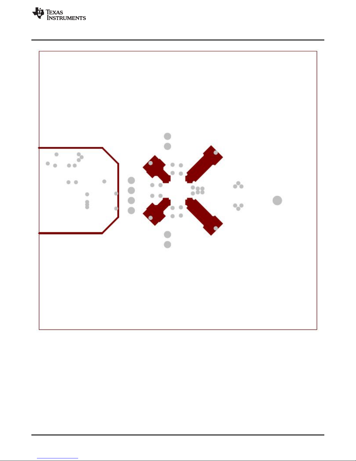
7.2 Layer Prints
Figure 7 through Figure 14 illustrate the LMH2832EVM layer prints.
LMH2832 EVM Schematic, Layer Prints, and Bill of Materials
SLOU454–June 2016
Submit Documentation Feedback
Figure 7. Top Layer
Copyright © 2016, Texas Instruments Incorporated
LMH2832EVM-50 Evaluation Module
11
Page 12

LMH2832 EVM Schematic, Layer Prints, and Bill of Materials
www.ti.com
12
LMH2832EVM-50 Evaluation Module
Figure 8. Layer 2 Ground Plane
Copyright © 2016, Texas Instruments Incorporated
Submit Documentation Feedback
SLOU454–June 2016
Page 13

www.ti.com
LMH2832 EVM Schematic, Layer Prints, and Bill of Materials
SLOU454–June 2016
Submit Documentation Feedback
Figure 9. Layer 3 GND Plane
Copyright © 2016, Texas Instruments Incorporated
LMH2832EVM-50 Evaluation Module
13
Page 14

LMH2832 EVM Schematic, Layer Prints, and Bill of Materials
www.ti.com
14
LMH2832EVM-50 Evaluation Module
Figure 10. Layer 4 GND Plane
Copyright © 2016, Texas Instruments Incorporated
Submit Documentation Feedback
SLOU454–June 2016
Page 15

www.ti.com
LMH2832 EVM Schematic, Layer Prints, and Bill of Materials
SLOU454–June 2016
Submit Documentation Feedback
Figure 11. Layer 5 V+ Plane
Copyright © 2016, Texas Instruments Incorporated
LMH2832EVM-50 Evaluation Module
15
Page 16

LMH2832 EVM Schematic, Layer Prints, and Bill of Materials
www.ti.com
16
LMH2832EVM-50 Evaluation Module
Figure 12. Layer 6 Ground Plane
Copyright © 2016, Texas Instruments Incorporated
Submit Documentation Feedback
SLOU454–June 2016
Page 17
www.ti.com
LMH2832 EVM Schematic, Layer Prints, and Bill of Materials
SLOU454–June 2016
Submit Documentation Feedback
Figure 13. Layer 7 GND Plane
Copyright © 2016, Texas Instruments Incorporated
LMH2832EVM-50 Evaluation Module
17
Page 18

LMH2832 EVM Schematic, Layer Prints, and Bill of Materials
www.ti.com
18
LMH2832EVM-50 Evaluation Module
Figure 14. Bottom Layer
Copyright © 2016, Texas Instruments Incorporated
Submit Documentation Feedback
SLOU454–June 2016
Page 19

www.ti.com
LMH2832 EVM Schematic, Layer Prints, and Bill of Materials
19
SLOU454–June 2016
Submit Documentation Feedback
Copyright © 2016, Texas Instruments Incorporated
LMH2832EVM-50 Evaluation Module
7.3 Bill of Materials
Table 5 lists the EVM bill of materials.
Table 5. LMH2832EVM Bill of Materials
Designator Qty Value Description PackageReference PartNumber Manufacturer Alternate Part
Number
Alternate
Manufacturer
!PCB 1 Printed Circuit Board HSP010 Any - C2, C3, C7, C8, C9,
C10
6 0.01uF CAP, CERM, 0.01uF, 25V, +/-5%, C0G/NP0, 0603 0603 C1608C0G1E103J TDK
C5, C38 2 0.1uF CAP, CERM, 0.1uF, 10V, +/-10%, X5R, 0402 0402 C1005X5R1A104K TDK - C6, C39 2 0.01uF CAP, CERM, 0.01uF, 16V, +/-10%, X7R, 0402 0402 C1005X7R1C103K TDK
C15 1 10uF CAP, TANT, 10uF, 10V, +/-10%, 0.9 ohm, 3216-18 SMD 3216-18 TPSA106K010R0900 AVX
C16, C19, C20, C23,
C24, C27, C29, C31
8 0.01uF CAP, CERM, 0.01uF, 25V, +/-10%, X7R, 0402 0402 C1005X7R1E103K TDK
C17, C18, C21, C22,
C25, C26, C28, C30
8 1000pF CAP, CERM, 1000pF, 25V, +/-5%, C0G/NP0, 0402 0402 C1005C0G1E102J TDK
C32, C33, C34, C35 4 1000pF CAP, CERM, 1000pF, 50V, +/-10%, X7R, 0603 0603 C0603C102K5RACTU Kemet
C36, C37 2 47pF CAP, CERM, 47 pF, 50 V, +/- 5%, C0G/NP0, 0402 0402 GRM1555C1H470JA01D MuRata
C40, C49 2 10uF CAP, CERM, 10uF, 16V, +/-10%, X5R, 0805 0805 EMK212BJ106KG-T Taiyo Yuden
D1 1 40V Diode, Schottky, 40V, 1A, SMB SMB 10BQ040TRPBF International Rectifier
H1, H2, H3, H4 4 Machine Screw, Round, #4-40 x 1/4, Nylon, Philips panhead Screw NY PMS 440 0025 PH B&F Fastener Supply
H5, H6, H7, H8 4 Standoff, Hex, 0.5"L #4-40 Nylon Standoff 1902C Keystone - J1, J3, J5, J7, J9, J11 6 Connector, SMT, End launch SMA 50 ohm SMA End Launch 142-0701-851 Emerson Network Power - J6, J8 2 Header, TH, 100mil, 2x1, Gold plated, 230 mil above insulator TSW-102-07-G-S TSW-102-07-G-S Samtec, Inc. - J13 1 MINI USB 2.0 SMT TYPE AB 5 CONTACTS R/A, SMD 9.2x9.9x4 mm 651305142821 Wurth Elektronik eiSos
L1 1 330 ohm 1.5A Ferrite Bead, 330 ohm @ 100MHz, SMD 0603 BLM18SG331TN1D MuRata
LBL1 1 Thermal Transfer Printable Labels, 0.650" W x 0.200" H - 10,000 per roll PCB Label 0.650"H
x 0.200"W
THT-14-423-10 Brady - -
R1, R4, R5, R6, R14,
R15, R16, R18, R19,
R20, R27, R28
12 0 RES, 0 ohm, 5%, 0.1W, 0603 0603 CRCW06030000Z0EA Vishay-Dale
R7, R8, R9, R10 4 40.2 RES, 40.2, 1%, 0.1 W, 0603 0603 CRCW060340R2FKEA Vishay-Dale
R21, R22 2 10.0k RES, 10.0k ohm, 1%, 0.063W, 0402 0402 CRCW040210K0FKED Vishay-Dale
R23, R24, R25, R26 4 22.1 RES, 22.1 ohm, 1%, 0.063W, 0402 0402 CRCW040222R1FKED Vishay-Dale
SH-J6_1-OPEN, SH-
J8_1-OPEN
2 1x2 Shunt, 100mil, Gold plated, Black 382811-6 AMP
T1, T2 2 Transformer, SMT 4.26x3.8mm MABA-011038 MACOM
T3, T4 2 Transformer, SMT 3.94x3.83mm ETC1-1-13TR MACOM
TP1 1 Red Test Point, TH, Multipurpose, Red 5010 Keystone Electronics
TP2, TP3 2 Black Test Point, TH, Multipurpose, Black 5011 Keystone Electronics
U1 1 Fully-Differential, Dual DVGA, DOCSIS 3.x Return Path ADC Driver,
RHA0040A
RHA0040A LMH2832IRHAR Texas Instruments LMH2832IRHAT Texas Instruments
U2 1 USB FIFO IC, 28SSOP SSOP28 FT245RL FTDI
U3 1 Ultra Low Noise, 150mA Linear Regulator for RF/Analog Circuits Requires No
Bypass Capacitor, 6-pin LLP, Pb-Free
SDB06A LP5900SD-1.8/NOPB Texas Instruments
Page 20
LMH2832 EVM Schematic, Layer Prints, and Bill of Materials
www.ti.com
20
SLOU454–June 2016
Submit Documentation Feedback
Copyright © 2016, Texas Instruments Incorporated
LMH2832EVM-50 Evaluation Module
Table 5. LMH2832EVM Bill of Materials (continued)
Designator Qty Value Description PackageReference PartNumber Manufacturer Alternate Part
Number
Alternate
Manufacturer
Z1, Z2 2 0.2uF Filter, LC, 0.2uF, 1806, SMT 1806 NFM41PC204F1H3L MuRata
C1, C4 0 0.01uF CAP, CERM, 0.01uF, 25V, +/-5%, C0G/NP0, 0603 0603 C1608C0G1E103J TDK
C11, C12, C13, C14 0 CAP, CERM, xxxF, xxV, [TempCo], xx%, [PackageReference] 0603 Used in BOM report Used in BOM report - C41, C42, C43, C44,
C45, C46, C47, C48
0 CAP, CERM, xxxF, xxV, [TempCo], xx%, [PackageReference] 0402 Used in BOM report Used in BOM report - -
FID1, FID2, FID3 0 Fiducial mark. There is nothing to buy or mount. Fiducial N/A N/A
J2, J4, J10, J12 0 Connector, SMT, End launch SMA 50 ohm SMA End Launch 142-0701-851 Emerson Network Power - R2, R13, R17, R29,
R30, R31, R32, R33,
R34, R35, R36
0 RES, xxx ohm, x%, xW, [PackageReference] 0603 Used in BOM report Used in BOM report - -
R3 0 0 RES, 0 ohm, 5%, 0.1W, 0603 0603 CRCW06030000Z0EA Vishay-Dale
R11, R12, R37, R38,
R39, R40
0 49.9 RES, 49.9 ohm, 1%, 0.1W, 0603 0603 CRCW060349R9FKEA Vishay-Dale
Notes: Unless otherwise noted in the Alternate PartNumber and/or Alternate Manufacturer columns, all parts may be substituted with equivalents.
Page 21

STANDARD TERMS AND CONDITIONS FOR EVALUATION MODULES
1. Delivery: TI delivers TI evaluation boards, kits, or modules, including any accompanying demonstration software, components, or
documentation (collectively, an “EVM” or “EVMs”) to the User (“User”) in accordance with the terms and conditions set forth herein.
Acceptance of the EVM is expressly subject to the following terms and conditions.
1.1 EVMs are intended solely for product or software developers for use in a research and development setting to facilitate feasibility
evaluation, experimentation, or scientific analysis of TI semiconductors products. EVMs have no direct function and are not
finished products. EVMs shall not be directly or indirectly assembled as a part or subassembly in any finished product. For
clarification, any software or software tools provided with the EVM (“Software”) shall not be subject to the terms and conditions
set forth herein but rather shall be subject to the applicable terms and conditions that accompany such Software
1.2 EVMs are not intended for consumer or household use. EVMs may not be sold, sublicensed, leased, rented, loaned, assigned,
or otherwise distributed for commercial purposes by Users, in whole or in part, or used in any finished product or production
system.
2 Limited Warranty and Related Remedies/Disclaimers:
2.1 These terms and conditions do not apply to Software. The warranty, if any, for Software is covered in the applicable Software
License Agreement.
2.2 TI warrants that the TI EVM will conform to TI's published specifications for ninety (90) days after the date TI delivers such EVM
to User. Notwithstanding the foregoing, TI shall not be liable for any defects that are caused by neglect, misuse or mistreatment
by an entity other than TI, including improper installation or testing, or for any EVMs that have been altered or modified in any
way by an entity other than TI. Moreover, TI shall not be liable for any defects that result from User's design, specifications or
instructions for such EVMs. Testing and other quality control techniques are used to the extent TI deems necessary or as
mandated by government requirements. TI does not test all parameters of each EVM.
2.3 If any EVM fails to conform to the warranty set forth above, TI's sole liability shall be at its option to repair or replace such EVM,
or credit User's account for such EVM. TI's liability under this warranty shall be limited to EVMs that are returned during the
warranty period to the address designated by TI and that are determined by TI not to conform to such warranty. If TI elects to
repair or replace such EVM, TI shall have a reasonable time to repair such EVM or provide replacements. Repaired EVMs shall
be warranted for the remainder of the original warranty period. Replaced EVMs shall be warranted for a new full ninety (90) day
warranty period.
3 Regulatory Notices:
3.1 United States
3.1.1 Notice applicable to EVMs not FCC-Approved:
This kit is designed to allow product developers to evaluate electronic components, circuitry, or software associated with the kit
to determine whether to incorporate such items in a finished product and software developers to write software applications for
use with the end product. This kit is not a finished product and when assembled may not be resold or otherwise marketed unless
all required FCC equipment authorizations are first obtained. Operation is subject to the condition that this product not cause
harmful interference to licensed radio stations and that this product accept harmful interference. Unless the assembled kit is
designed to operate under part 15, part 18 or part 95 of this chapter, the operator of the kit must operate under the authority of
an FCC license holder or must secure an experimental authorization under part 5 of this chapter.
3.1.2 For EVMs annotated as FCC – FEDERAL COMMUNICATIONS COMMISSION Part 15 Compliant:
CAUTION
This device complies with part 15 of the FCC Rules. Operation is subject to the following two conditions: (1) This device may not
cause harmful interference, and (2) this device must accept any interference received, including interference that may cause
undesired operation.
Changes or modifications not expressly approved by the party responsible for compliance could void the user's authority to
operate the equipment.
FCC Interference Statement for Class A EVM devices
NOTE: This equipment has been tested and found to comply with the limits for a Class A digital device, pursuant to part 15 of
the FCC Rules. These limits are designed to provide reasonable protection against harmful interference when the equipment is
operated in a commercial environment. This equipment generates, uses, and can radiate radio frequency energy and, if not
installed and used in accordance with the instruction manual, may cause harmful interference to radio communications.
Operation of this equipment in a residential area is likely to cause harmful interference in which case the user will be required to
correct the interference at his own expense.
SPACER
SPACER
SPACER
SPACER
SPACER
SPACER
SPACER
SPACER
Page 22

FCC Interference Statement for Class B EVM devices
NOTE: This equipment has been tested and found to comply with the limits for a Class B digital device, pursuant to part 15 of
the FCC Rules. These limits are designed to provide reasonable protection against harmful interference in a residential
installation. This equipment generates, uses and can radiate radio frequency energy and, if not installed and used in accordance
with the instructions, may cause harmful interference to radio communications. However, there is no guarantee that interference
will not occur in a particular installation. If this equipment does cause harmful interference to radio or television reception, which
can be determined by turning the equipment off and on, the user is encouraged to try to correct the interference by one or more
of the following measures:
• Reorient or relocate the receiving antenna.
• Increase the separation between the equipment and receiver.
• Connect the equipment into an outlet on a circuit different from that to which the receiver is connected.
• Consult the dealer or an experienced radio/TV technician for help.
3.2 Canada
3.2.1 For EVMs issued with an Industry Canada Certificate of Conformance to RSS-210
Concerning EVMs Including Radio Transmitters:
This device complies with Industry Canada license-exempt RSS standard(s). Operation is subject to the following two conditions:
(1) this device may not cause interference, and (2) this device must accept any interference, including interference that may
cause undesired operation of the device.
Concernant les EVMs avec appareils radio:
Le présent appareil est conforme aux CNR d'Industrie Canada applicables aux appareils radio exempts de licence. L'exploitation
est autorisée aux deux conditions suivantes: (1) l'appareil ne doit pas produire de brouillage, et (2) l'utilisateur de l'appareil doit
accepter tout brouillage radioélectrique subi, même si le brouillage est susceptible d'en compromettre le fonctionnement.
Concerning EVMs Including Detachable Antennas:
Under Industry Canada regulations, this radio transmitter may only operate using an antenna of a type and maximum (or lesser)
gain approved for the transmitter by Industry Canada. To reduce potential radio interference to other users, the antenna type
and its gain should be so chosen that the equivalent isotropically radiated power (e.i.r.p.) is not more than that necessary for
successful communication. This radio transmitter has been approved by Industry Canada to operate with the antenna types
listed in the user guide with the maximum permissible gain and required antenna impedance for each antenna type indicated.
Antenna types not included in this list, having a gain greater than the maximum gain indicated for that type, are strictly prohibited
for use with this device.
Concernant les EVMs avec antennes détachables
Conformément à la réglementation d'Industrie Canada, le présent émetteur radio peut fonctionner avec une antenne d'un type et
d'un gain maximal (ou inférieur) approuvé pour l'émetteur par Industrie Canada. Dans le but de réduire les risques de brouillage
radioélectrique à l'intention des autres utilisateurs, il faut choisir le type d'antenne et son gain de sorte que la puissance isotrope
rayonnée équivalente (p.i.r.e.) ne dépasse pas l'intensité nécessaire à l'établissement d'une communication satisfaisante. Le
présent émetteur radio a été approuvé par Industrie Canada pour fonctionner avec les types d'antenne énumérés dans le
manuel d’usage et ayant un gain admissible maximal et l'impédance requise pour chaque type d'antenne. Les types d'antenne
non inclus dans cette liste, ou dont le gain est supérieur au gain maximal indiqué, sont strictement interdits pour l'exploitation de
l'émetteur
3.3 Japan
3.3.1 Notice for EVMs delivered in Japan: Please see http://www.tij.co.jp/lsds/ti_ja/general/eStore/notice_01.page 日本国内に
輸入される評価用キット、ボードについては、次のところをご覧ください。
http://www.tij.co.jp/lsds/ti_ja/general/eStore/notice_01.page
3.3.2 Notice for Users of EVMs Considered “Radio Frequency Products” in Japan: EVMs entering Japan may not be certified
by TI as conforming to Technical Regulations of Radio Law of Japan.
If User uses EVMs in Japan, not certified to Technical Regulations of Radio Law of Japan, User is required by Radio Law of
Japan to follow the instructions below with respect to EVMs:
1. Use EVMs in a shielded room or any other test facility as defined in the notification #173 issued by Ministry of Internal
Affairs and Communications on March 28, 2006, based on Sub-section 1.1 of Article 6 of the Ministry’s Rule for
Enforcement of Radio Law of Japan,
2. Use EVMs only after User obtains the license of Test Radio Station as provided in Radio Law of Japan with respect to
EVMs, or
3. Use of EVMs only after User obtains the Technical Regulations Conformity Certification as provided in Radio Law of Japan
with respect to EVMs. Also, do not transfer EVMs, unless User gives the same notice above to the transferee. Please note
that if User does not follow the instructions above, User will be subject to penalties of Radio Law of Japan.
SPACER
SPACER
SPACER
SPACER
SPACER
Page 23

【無線電波を送信する製品の開発キットをお使いになる際の注意事項】 開発キットの中には技術基準適合証明を受けて
いないものがあります。 技術適合証明を受けていないもののご使用に際しては、電波法遵守のため、以下のいずれかの
措置を取っていただく必要がありますのでご注意ください。
1. 電波法施行規則第6条第1項第1号に基づく平成18年3月28日総務省告示第173号で定められた電波暗室等の試験設備でご使用
いただく。
2. 実験局の免許を取得後ご使用いただく。
3. 技術基準適合証明を取得後ご使用いただく。
なお、本製品は、上記の「ご使用にあたっての注意」を譲渡先、移転先に通知しない限り、譲渡、移転できないものとします。
上記を遵守頂けない場合は、電波法の罰則が適用される可能性があることをご留意ください。 日本テキサス・イ
ンスツルメンツ株式会社
東京都新宿区西新宿6丁目24番1号
西新宿三井ビル
3.3.3 Notice for EVMs for Power Line Communication: Please see http://www.tij.co.jp/lsds/ti_ja/general/eStore/notice_02.page
電力線搬送波通信についての開発キットをお使いになる際の注意事項については、次のところをご覧くださ
い。http://www.tij.co.jp/lsds/ti_ja/general/eStore/notice_02.page
SPACER
4 EVM Use Restrictions and Warnings:
4.1 EVMS ARE NOT FOR USE IN FUNCTIONAL SAFETY AND/OR SAFETY CRITICAL EVALUATIONS, INCLUDING BUT NOT
LIMITED TO EVALUATIONS OF LIFE SUPPORT APPLICATIONS.
4.2 User must read and apply the user guide and other available documentation provided by TI regarding the EVM prior to handling
or using the EVM, including without limitation any warning or restriction notices. The notices contain important safety information
related to, for example, temperatures and voltages.
4.3 Safety-Related Warnings and Restrictions:
4.3.1 User shall operate the EVM within TI’s recommended specifications and environmental considerations stated in the user
guide, other available documentation provided by TI, and any other applicable requirements and employ reasonable and
customary safeguards. Exceeding the specified performance ratings and specifications (including but not limited to input
and output voltage, current, power, and environmental ranges) for the EVM may cause personal injury or death, or
property damage. If there are questions concerning performance ratings and specifications, User should contact a TI
field representative prior to connecting interface electronics including input power and intended loads. Any loads applied
outside of the specified output range may also result in unintended and/or inaccurate operation and/or possible
permanent damage to the EVM and/or interface electronics. Please consult the EVM user guide prior to connecting any
load to the EVM output. If there is uncertainty as to the load specification, please contact a TI field representative.
During normal operation, even with the inputs and outputs kept within the specified allowable ranges, some circuit
components may have elevated case temperatures. These components include but are not limited to linear regulators,
switching transistors, pass transistors, current sense resistors, and heat sinks, which can be identified using the
information in the associated documentation. When working with the EVM, please be aware that the EVM may become
very warm.
4.3.2 EVMs are intended solely for use by technically qualified, professional electronics experts who are familiar with the
dangers and application risks associated with handling electrical mechanical components, systems, and subsystems.
User assumes all responsibility and liability for proper and safe handling and use of the EVM by User or its employees,
affiliates, contractors or designees. User assumes all responsibility and liability to ensure that any interfaces (electronic
and/or mechanical) between the EVM and any human body are designed with suitable isolation and means to safely
limit accessible leakage currents to minimize the risk of electrical shock hazard. User assumes all responsibility and
liability for any improper or unsafe handling or use of the EVM by User or its employees, affiliates, contractors or
designees.
4.4 User assumes all responsibility and liability to determine whether the EVM is subject to any applicable international, federal,
state, or local laws and regulations related to User’s handling and use of the EVM and, if applicable, User assumes all
responsibility and liability for compliance in all respects with such laws and regulations. User assumes all responsibility and
liability for proper disposal and recycling of the EVM consistent with all applicable international, federal, state, and local
requirements.
5. Accuracy of Information: To the extent TI provides information on the availability and function of EVMs, TI attempts to be as accurate
as possible. However, TI does not warrant the accuracy of EVM descriptions, EVM availability or other information on its websites as
accurate, complete, reliable, current, or error-free.
SPACER
SPACER
SPACER
SPACER
SPACER
SPACER
Page 24

SPACER
6. Disclaimers:
6.1 EXCEPT AS SET FORTH ABOVE, EVMS AND ANY WRITTEN DESIGN MATERIALS PROVIDED WITH THE EVM (AND THE
DESIGN OF THE EVM ITSELF) ARE PROVIDED "AS IS" AND "WITH ALL FAULTS." TI DISCLAIMS ALL OTHER
WARRANTIES, EXPRESS OR IMPLIED, REGARDING SUCH ITEMS, INCLUDING BUT NOT LIMITED TO ANY IMPLIED
WARRANTIES OF MERCHANTABILITY OR FITNESS FOR A PARTICULAR PURPOSE OR NON-INFRINGEMENT OF ANY
THIRD PARTY PATENTS, COPYRIGHTS, TRADE SECRETS OR OTHER INTELLECTUAL PROPERTY RIGHTS.
6.2 EXCEPT FOR THE LIMITED RIGHT TO USE THE EVM SET FORTH HEREIN, NOTHING IN THESE TERMS AND
CONDITIONS SHALL BE CONSTRUED AS GRANTING OR CONFERRING ANY RIGHTS BY LICENSE, PATENT, OR ANY
OTHER INDUSTRIAL OR INTELLECTUAL PROPERTY RIGHT OF TI, ITS SUPPLIERS/LICENSORS OR ANY OTHER THIRD
PARTY, TO USE THE EVM IN ANY FINISHED END-USER OR READY-TO-USE FINAL PRODUCT, OR FOR ANY
INVENTION, DISCOVERY OR IMPROVEMENT MADE, CONCEIVED OR ACQUIRED PRIOR TO OR AFTER DELIVERY OF
THE EVM.
7. USER'S INDEMNITY OBLIGATIONS AND REPRESENTATIONS. USER WILL DEFEND, INDEMNIFY AND HOLD TI, ITS
LICENSORS AND THEIR REPRESENTATIVES HARMLESS FROM AND AGAINST ANY AND ALL CLAIMS, DAMAGES, LOSSES,
EXPENSES, COSTS AND LIABILITIES (COLLECTIVELY, "CLAIMS") ARISING OUT OF OR IN CONNECTION WITH ANY
HANDLING OR USE OF THE EVM THAT IS NOT IN ACCORDANCE WITH THESE TERMS AND CONDITIONS. THIS OBLIGATION
SHALL APPLY WHETHER CLAIMS ARISE UNDER STATUTE, REGULATION, OR THE LAW OF TORT, CONTRACT OR ANY
OTHER LEGAL THEORY, AND EVEN IF THE EVM FAILS TO PERFORM AS DESCRIBED OR EXPECTED.
8. Limitations on Damages and Liability:
8.1 General Limitations. IN NO EVENT SHALL TI BE LIABLE FOR ANY SPECIAL, COLLATERAL, INDIRECT, PUNITIVE,
INCIDENTAL, CONSEQUENTIAL, OR EXEMPLARY DAMAGES IN CONNECTION WITH OR ARISING OUT OF THESE
TERMS ANDCONDITIONS OR THE USE OF THE EVMS PROVIDED HEREUNDER, REGARDLESS OF WHETHER TI HAS
BEEN ADVISED OF THE POSSIBILITY OF SUCH DAMAGES. EXCLUDED DAMAGES INCLUDE, BUT ARE NOT LIMITED
TO, COST OF REMOVAL OR REINSTALLATION, ANCILLARY COSTS TO THE PROCUREMENT OF SUBSTITUTE GOODS
OR SERVICES, RETESTING, OUTSIDE COMPUTER TIME, LABOR COSTS, LOSS OF GOODWILL, LOSS OF PROFITS,
LOSS OF SAVINGS, LOSS OF USE, LOSS OF DATA, OR BUSINESS INTERRUPTION. NO CLAIM, SUIT OR ACTION SHALL
BE BROUGHT AGAINST TI MORE THAN ONE YEAR AFTER THE RELATED CAUSE OF ACTION HAS OCCURRED.
8.2 Specific Limitations. IN NO EVENT SHALL TI'S AGGREGATE LIABILITY FROM ANY WARRANTY OR OTHER OBLIGATION
ARISING OUT OF OR IN CONNECTION WITH THESE TERMS AND CONDITIONS, OR ANY USE OF ANY TI EVM
PROVIDED HEREUNDER, EXCEED THE TOTAL AMOUNT PAID TO TI FOR THE PARTICULAR UNITS SOLD UNDER
THESE TERMS AND CONDITIONS WITH RESPECT TO WHICH LOSSES OR DAMAGES ARE CLAIMED. THE EXISTENCE
OF MORE THAN ONE CLAIM AGAINST THE PARTICULAR UNITS SOLD TO USER UNDER THESE TERMS AND
CONDITIONS SHALL NOT ENLARGE OR EXTEND THIS LIMIT.
9. Return Policy. Except as otherwise provided, TI does not offer any refunds, returns, or exchanges. Furthermore, no return of EVM(s)
will be accepted if the package has been opened and no return of the EVM(s) will be accepted if they are damaged or otherwise not in
a resalable condition. If User feels it has been incorrectly charged for the EVM(s) it ordered or that delivery violates the applicable
order, User should contact TI. All refunds will be made in full within thirty (30) working days from the return of the components(s),
excluding any postage or packaging costs.
10. Governing Law: These terms and conditions shall be governed by and interpreted in accordance with the laws of the State of Texas,
without reference to conflict-of-laws principles. User agrees that non-exclusive jurisdiction for any dispute arising out of or relating to
these terms and conditions lies within courts located in the State of Texas and consents to venue in Dallas County, Texas.
Notwithstanding the foregoing, any judgment may be enforced in any United States or foreign court, and TI may seek injunctive relief
in any United States or foreign court.
Mailing Address: Texas Instruments, Post Office Box 655303, Dallas, Texas 75265
spacer
Copyright © 2015, Texas Instruments Incorporated
Page 25

IMPORTANT NOTICE
Texas Instruments Incorporated and its subsidiaries (TI) reserve the right to make corrections, enhancements, improvements and other
changes to its semiconductor products and services per JESD46, latest issue, and to discontinue any product or service per JESD48, latest
issue. Buyers should obtain the latest relevant information before placing orders and should verify that such information is current and
complete. All semiconductor products (also referred to herein as “components”) are sold subject to TI’s terms and conditions of sale
supplied at the time of order acknowledgment.
TI warrants performance of its components to the specifications applicable at the time of sale, in accordance with the warranty in TI’s terms
and conditions of sale of semiconductor products. Testing and other quality control techniques are used to the extent TI deems necessary
to support this warranty. Except where mandated by applicable law, testing of all parameters of each component is not necessarily
performed.
TI assumes no liability for applications assistance or the design of Buyers’ products. Buyers are responsible for their products and
applications using TI components. To minimize the risks associated with Buyers’ products and applications, Buyers should provide
adequate design and operating safeguards.
TI does not warrant or represent that any license, either express or implied, is granted under any patent right, copyright, mask work right, or
other intellectual property right relating to any combination, machine, or process in which TI components or services are used. Information
published by TI regarding third-party products or services does not constitute a license to use such products or services or a warranty or
endorsement thereof. Use of such information may require a license from a third party under the patents or other intellectual property of the
third party, or a license from TI under the patents or other intellectual property of TI.
Reproduction of significant portions of TI information in TI data books or data sheets is permissible only if reproduction is without alteration
and is accompanied by all associated warranties, conditions, limitations, and notices. TI is not responsible or liable for such altered
documentation. Information of third parties may be subject to additional restrictions.
Resale of TI components or services with statements different from or beyond the parameters stated by TI for that component or service
voids all express and any implied warranties for the associated TI component or service and is an unfair and deceptive business practice.
TI is not responsible or liable for any such statements.
Buyer acknowledges and agrees that it is solely responsible for compliance with all legal, regulatory and safety-related requirements
concerning its products, and any use of TI components in its applications, notwithstanding any applications-related information or support
that may be provided by TI. Buyer represents and agrees that it has all the necessary expertise to create and implement safeguards which
anticipate dangerous consequences of failures, monitor failures and their consequences, lessen the likelihood of failures that might cause
harm and take appropriate remedial actions. Buyer will fully indemnify TI and its representatives against any damages arising out of the use
of any TI components in safety-critical applications.
In some cases, TI components may be promoted specifically to facilitate safety-related applications. With such components, TI’s goal is to
help enable customers to design and create their own end-product solutions that meet applicable functional safety standards and
requirements. Nonetheless, such components are subject to these terms.
No TI components are authorized for use in FDA Class III (or similar life-critical medical equipment) unless authorized officers of the parties
have executed a special agreement specifically governing such use.
Only those TI components which TI has specifically designated as military grade or “enhanced plastic” are designed and intended for use in
military/aerospace applications or environments. Buyer acknowledges and agrees that any military or aerospace use of TI components
which have not been so designated is solely at the Buyer's risk, and that Buyer is solely responsible for compliance with all legal and
regulatory requirements in connection with such use.
TI has specifically designated certain components as meeting ISO/TS16949 requirements, mainly for automotive use. In any case of use of
non-designated products, TI will not be responsible for any failure to meet ISO/TS16949.
Products Applications
Audio www.ti.com/audio Automotive and Transportation www.ti.com/automotive
Amplifiers amplifier.ti.com Communications and Telecom www.ti.com/communications
Data Converters dataconverter.ti.com Computers and Peripherals www.ti.com/computers
DLP® Products www.dlp.com Consumer Electronics www.ti.com/consumer-apps
DSP dsp.ti.com Energy and Lighting www.ti.com/energy
Clocks and Timers www.ti.com/clocks Industrial www.ti.com/industrial
Interface interface.ti.com Medical www.ti.com/medical
Logic logic.ti.com Security www.ti.com/security
Power Mgmt power.ti.com Space, Avionics and Defense www.ti.com/space-avionics-defense
Microcontrollers microcontroller.ti.com Video and Imaging www.ti.com/video
RFID www.ti-rfid.com
OMAP Applications Processors www.ti.com/omap TI E2E Community e2e.ti.com
Wireless Connectivity www.ti.com/wirelessconnectivity
Mailing Address: Texas Instruments, Post Office Box 655303, Dallas, Texas 75265
Copyright © 2016, Texas Instruments Incorporated
 Loading...