
LMH1980
www.ti.com
LMH1980 Auto-Detecting SD/HD/PC Video Sync Separator
Check for Samples: LMH1980
1
FEATURES
2
• Analog Video Sync Separation for NTSC, PAL,
480I/P, 576I/P, 720P, 1080I/P/PsF, and Many
VESA-Compatible Timing Formats
• Composite Video (CVBS), S-Video (Y/C), and
Component Video (YPBPR/GBR) and PC
Graphics (RGsB) Interfaces
• SD/PC Bi-Level Sync & HD Tri-Level Sync
Compatible
• Composite, Horizontal, and Vertical Sync
Outputs
• Burst/Back Porch Timing, Odd/Even Field, and
HD Detect Flag outputs
• Automatic Video Format Detection
• Fixed-Level Sync Slicing for Video Inputs from
0.5 to 2 V
• 3.3V to 5V Supply Operation
APPLICATIONS
• Consumer, Professional, Automotive &
Industrial Video
• Video Capture, Editing, and Processing
• Genlock Circuits
• Surveillance & Security Video Systems
• Set-Top Boxes (STB) & Digital Video
Recorders (DVR)
• LCD / Plasma Displays and Video Projectors
• Machine Vision and Inspection Systems
• Video Trigger Oscilloscopes and Waveform
Monitors
PP
SNLS263A –JULY 2007–REVISED MARCH 2013
DESCRIPTION
The LMH1980 is an auto-detecting SD/HD/PC video
sync separator ideal for use in a wide range of video
applications, such as automotive LCD monitors, video
capture & editing devices, surveillance & security
equipment, and machine vision and inspection
systems.
The LMH1980 accepts an analog video input signal
with either bi-level or tri-level sync and automatically
detects the video format, eliminating the need for
external R
sync separators (e.g.: LM1881). The outputs provide
timing signals in CMOS logic, including Composite,
Horizontal, and Vertical Syncs, Burst/Back Porch
Timing, and Odd/Even Field outputs. The HD flag
output (pin 5) provides a logic low signal only when a
valid HD video input with tri-level sync is detected.
The HD flag can be used to disable an external
switch-controlled SD chroma filter when HD video is
detected, or enable it when SD video is detected. For
non-standard video with bi-level sync and without
vertical serration pulses, a default vertical sync pulse
will be output and no horizontal sync pulses will be
output during the vertical sync interval.
The LMH1980 is available in a space-saving 10-lead
Mini-SO Package (VSSOP) and operates over a
temperature range of −40°C to +85°C.
resistor adjustment required by other
SET
1
Please be aware that an important notice concerning availability, standard warranty, and use in critical applications of
Texas Instruments semiconductor products and disclaimers thereto appears at the end of this data sheet.
2All trademarks are the property of their respective owners.
PRODUCTION DATA information is current as of publication date.
Products conform to specifications per the terms of the Texas
Instruments standard warranty. Production processing does not
necessarily include testing of all parameters.
Copyright © 2007–2013, Texas Instruments Incorporated
R
EXT
GND
V
CC
V
IN
HD
OEOUT
BPOUT
CSOUT
VSOUT
HSOUT
LMH1980
1
2
3
4
5
10
9
8
7
6
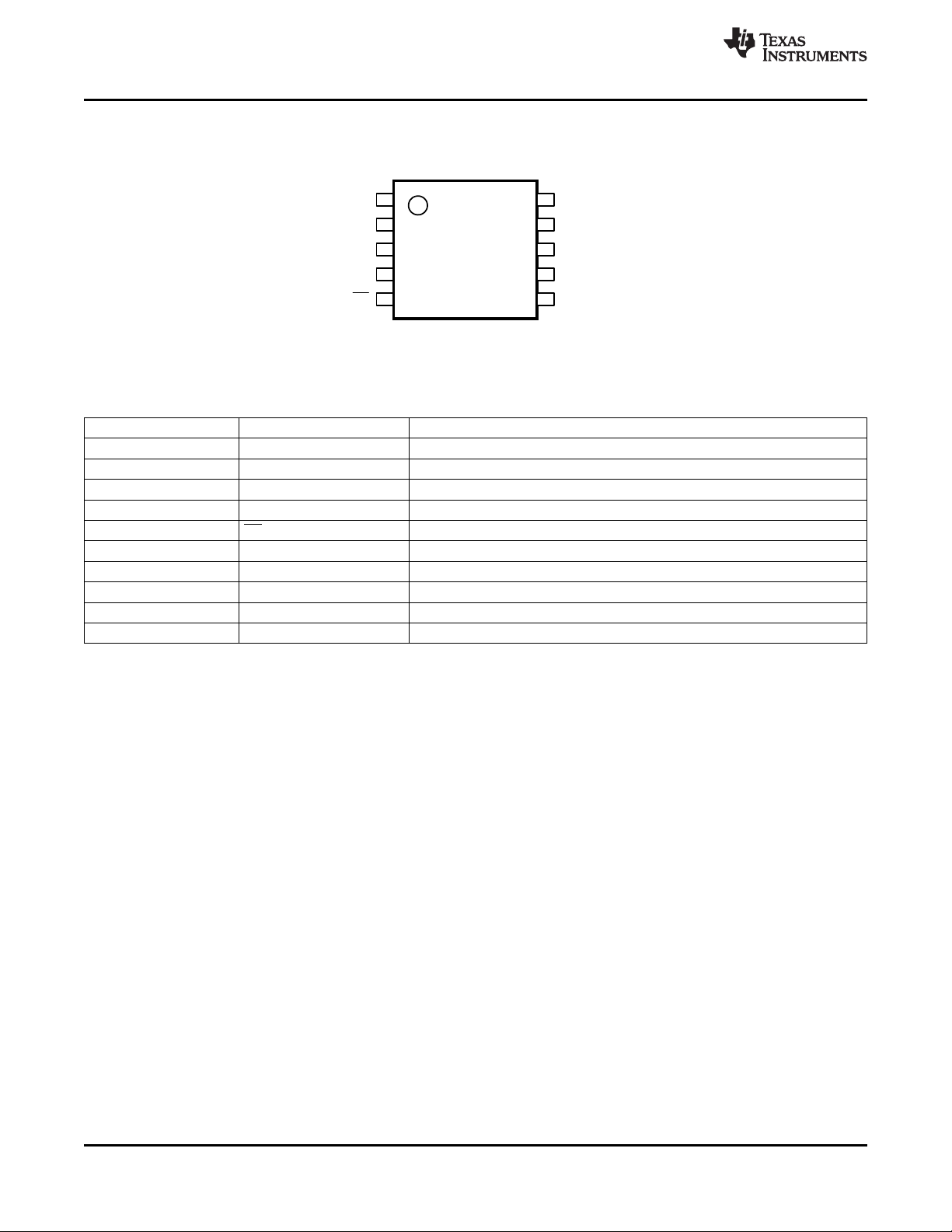
LMH1980
SNLS263A –JULY 2007–REVISED MARCH 2013
Connection Diagram
Top View
Figure 1. 10-Lead VSSOP Package
See Package Number DGS0010A
Pin Descriptions
Pin No. Pin Name Pin Description
1 R
EXT
2 GND Ground
3 V
4 V
CC
IN
5 HD HD Detect Flag Output
6 HSOUT Horizontal Sync Output
7 VSOUT Vertical Sync Output
8 CSOUT Composite Sync Output
9 BPOUT Burst/Back Porch Timing Output
10 OEOUT Odd/Even Field Output
Bias Current External Resistor
Supply Voltage
Analog Video Input
www.ti.com
2 Submit Documentation Feedback Copyright © 2007–2013, Texas Instruments Incorporated
Product Folder Links: LMH1980
LMH1980
www.ti.com
SNLS263A –JULY 2007–REVISED MARCH 2013
These devices have limited built-in ESD protection. The leads should be shorted together or the device placed in conductive foam
during storage or handling to prevent electrostatic damage to the MOS gates.
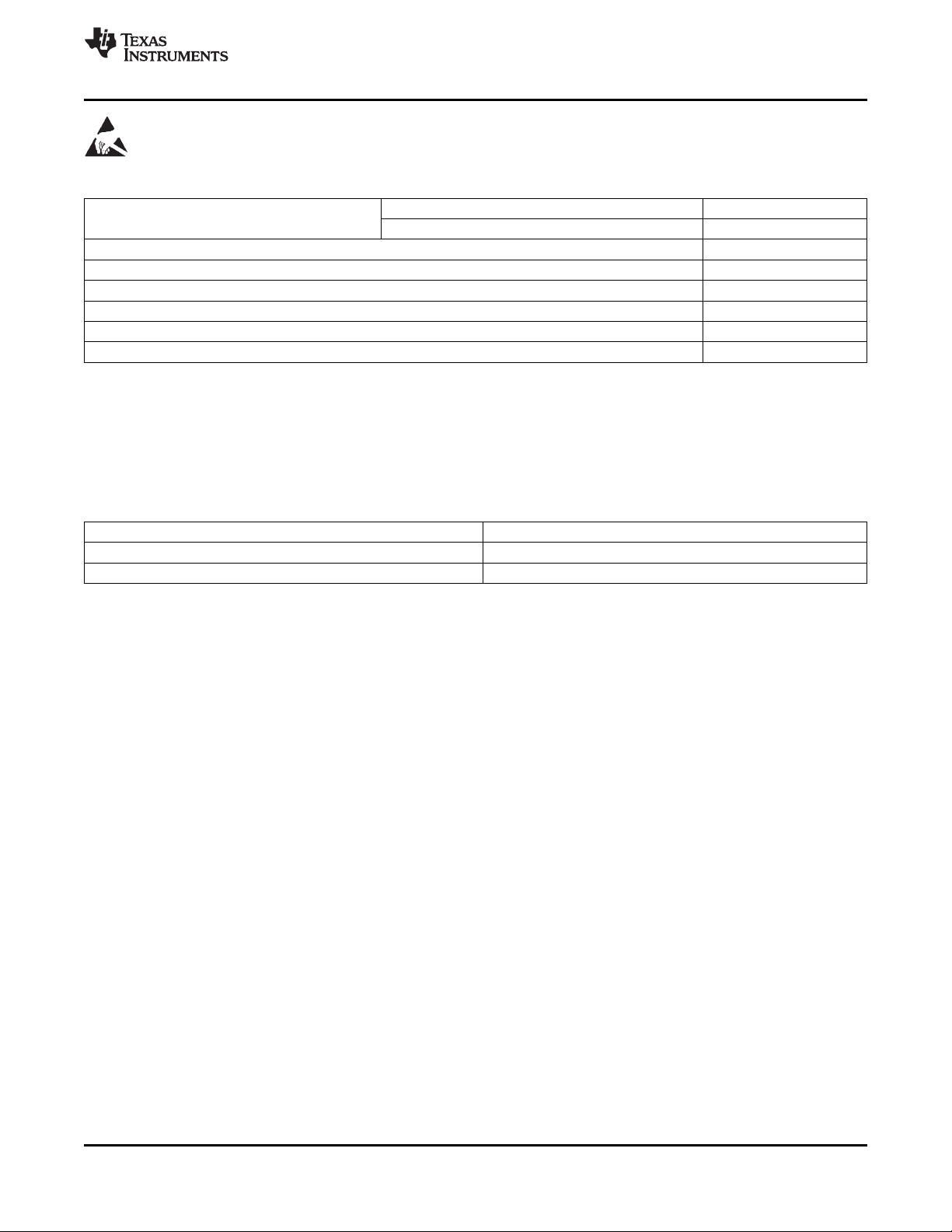
Absolute Maximum Ratings
ESD Tolerance
(3)
(1)(2)
Human Body Model 3.5 kV
Machine Model 350V
Supply Voltage, V
Video Input, V
IN
CC
−0.3V to VCC+ 0.3V
0V to 5.5V
Storage Temperature Range −65°C to +150°C
Lead Temperature (soldering 10 sec.) 300°C
Junction Temperature, T
JMAX
(4)
+150°C
Thermal Resistance, θJA(no airflow) 120°C/W
(1) Absolute Maximum Ratings indicate limits beyond which damage to the device may occur. Operating Ratings indicate conditions for
which the device is intended to be functional, but specific performance is not ensured. For ensured specifications and the test
conditions, see the Electrical Characteristics Tables.
(2) All voltages are measured with respect to GND, unless otherwise specified.
(3) Human Body Model, applicable std. MIL-STD-883, Method 3015.7. Machine Model, applicable std. JESD22-A115-A (ESD MM std. of
JEDEC)Field-Induced Charge-Device Model, applicable std. JESD22-C101-C (ESD FICDM std. of JEDEC).
(4) The maximum power dissipation is a function of T
PD= (T
Operating Ratings
Temperature Range
V
CC
Input Amplitude, V
- TA)/θJA. All numbers apply for packages soldered directly onto a PC board.
J(MAX)
(1)
(2)
IN-AMPL
, θJA. The maximum allowable power dissipation at any ambient temperature is
J(MAX)
−40°C to +85°C
3.3V −10% to 5V +10%
140 mV to VCC–V
IN-CLAMP
(1) Absolute Maximum Ratings indicate limits beyond which damage to the device may occur. Operating Ratings indicate conditions for
which the device is intended to be functional, but specific performance is not ensured. For ensured specifications and the test
conditions, see the Electrical Characteristics Tables.
(2) The maximum power dissipation is a function of T
PD= (T
- TA)/θJA. All numbers apply for packages soldered directly onto a PC board.
J(MAX)
, θJA. The maximum allowable power dissipation at any ambient temperature is
J(MAX)
Copyright © 2007–2013, Texas Instruments Incorporated Submit Documentation Feedback 3
Product Folder Links: LMH1980
LMH1980
SNLS263A –JULY 2007–REVISED MARCH 2013
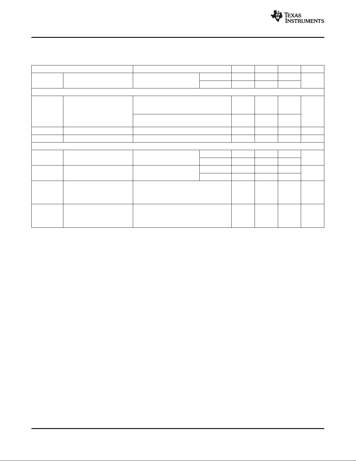
Electrical Characteristics
Unless otherwise specified, all limits are specified for TA= 25°C, VCC= 3.3V, R
(1)
EXT
pF.Boldface limits apply at the temperature extremes. See Figure 2 for Test Circuit.
Parameter Test Conditions Min
I
CC
Video Input Specifications
V
IN-SYNC
V
IN-CLAMP
V
IN-SLICE
Logic Output Specifications
V
OL
V
OH
T
SYNC-LOCK
T
VSOUT
Supply Current No input signal VCC= 3.3V 10.5 12.5
VCC= 5V 12.0 14.0
Input Sync Amplitude Amplitude from negative sync tip to video 0.14 0.30 0.60
blanking level for SD/EDTV bi-level sync
(5)
Amplitude from negative to positive sync tips 0.30 0.60 1.20
for HDTV tri-level sync
Input Sync Tip Clamp Level
(7)
Input Sync Slice Level Slicing level above V
(8)
(4) (6)
IN-CLAMP
(4)
Output Logic 0 See output load conditions VCC= 3.3V 0.3
above
VCC= 5V 0.5
Output Logic 1 See output load conditions VCC= 3.3V 3.0
above
VCC= 5V 4.5
Sync Lock Time Time for the output signals to be correct after 2 V
the video signal settles at VINfollowing a periods
significant input change. See START-UP
TIME for more information
Vertical Sync Output Pulse Serration Pulses in the Vertical Interval. See 3 H
Width Figure 3, Figure 4, Figure 5, Figure 6, periods
Figure 7, and Figure 8 for SDTV, EDTV &
HDTV Vertical Interval Timing
= 10 kΩ 1%, RL= 10 kΩ, CL< 10
(2)
Typ
(3)
Max
(2)
0.7 V
70 mV
www.ti.com
Units
mA
V
PP
V
V
(1) Electrical Table values apply only for factory testing conditions at the temperature indicated. Factory testing conditions result in very
limited self-heating of the device such that TJ= TA. Parametric performance indicated in the electrical tables is not ensured under
conditions of internal self-heating where TJ> TA.
(2) Limits are 100% production tested at 25°C. Limits over the operating temperature range are ensured through correlations using the
Statistical Quality Control (SQC) method.
(3) Typical values represent the most likely parametric norm at the time of characterization. Actual typical values may vary over time and
will also depend on the application and configuration. The typical values are not tested and are not specified on shipped production
material.
(4) V
(5) Tested with 480I signal.
IN-AMPL
plus V
IN-CLAMP
should not exceed VCC.
(6) Tested with 1080P signal.
(7) Maximum voltage offset (DC bounce) between 2 consecutive input sync tips must be less than 25 mVPP; otherwise, this may cause
incorrect output signals to occur.
(8) Outputs are negative-polarity logic signals, except for Odd/Even Field.
4 Submit Documentation Feedback Copyright © 2007–2013, Texas Instruments Incorporated
Product Folder Links: LMH1980
V
IN
CSOUT
HSOUT
BPOUT
VSOUT
OEOUT
COLOR
BURST
START OF FIELD 1
ODD FIELD
LINE # 1 3 4 5 6 7 9 10 11525 2 8
3H
H
3H 3H
T
VSOUT
= 3H
H
½ H
VERTICAL SYNC
SERRATION
TP2
Odd/Even
Field Output
2
1
TP3
Burst/Back
Porch Output
2
1
TP4
Composite
Sync Output
2
1
TP5
Vertical Sync
Output
2
1
TP6
Horizontal
Sync Output
2
1
R
6
100:
R
7
100:
R
8
100:
R
4
100:
R
5
100:
7
6
8
9
10
OEOUT
BPOUT
CSOUT
VSOUT
HSOUT
LMH1980
4
5
3
2
1
R
EXT
GND
V
CC
V
IN
HD
U2
R
2
10 k:
1%
C
5
0.1 PF
C
3
0.1 PF
+
C
4
10 PF
R
3
10 k:
R
10
100:
TP1
HD Detect Flag Output
2
1
J2
GND
TP7
GND
1
1
J1
V
CC
TP8
V
CC
1
1
R
9
100:
C
2
560 pF
C
1
*OPT
Q1
MMBT3904
R
1
75:
BNC
J3
LMH1980
www.ti.com
SNLS263A –JULY 2007–REVISED MARCH 2013
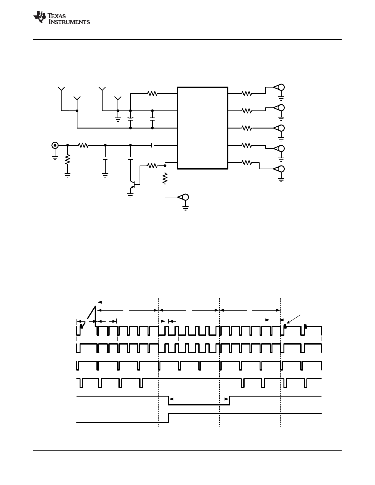
LMH1980 Test Circuit
Figure 2. Test Circuit
The LMH1980 test circuit is shown in Figure 2. The video generator should provide a clean, low-noise video input
signal with minimal sync pulse overshoot over 75Ω coaxial cable, which should be impedance-matched with a
75Ω load termination resistor to prevent unwanted signal distortion. The output waveforms should be monitored
using a low-capacitance probe on an oscilloscope with at least 500 MHz bandwidth. See PCB LAYOUT
CONSIDERATIONS for more information about signal and supply trace routing and component placement. Also,
refer to the “LMH1980 Evaluation Board Instruction Manual” Application Note (AN-1618 [SNLA096]).
SDTV Vertical Interval Timing Diagrams (NTSC, PAL, 480I, 576I)
Copyright © 2007–2013, Texas Instruments Incorporated Submit Documentation Feedback 5
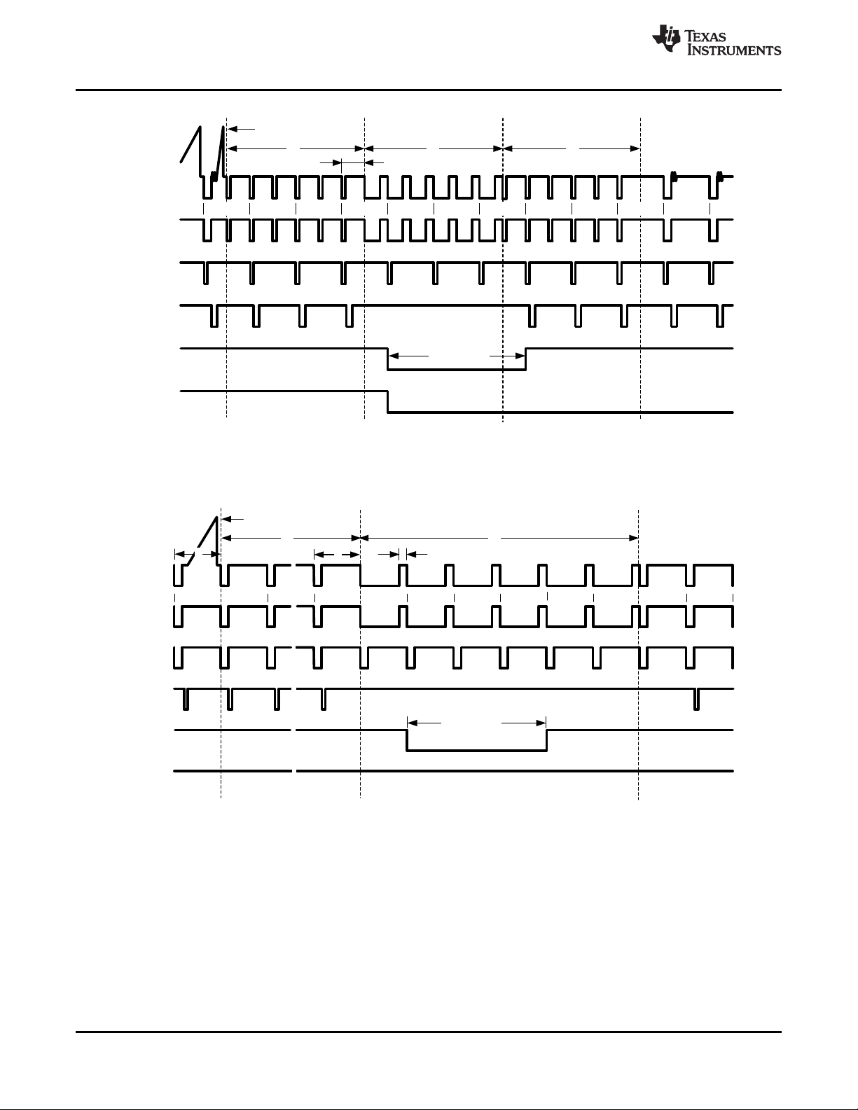
Figure 3. NTSC Odd Field Vertical Interval
Product Folder Links: LMH1980
V
IN
CSOUT
HSOUT
BPOUT
VSOUT
OEOUT
START OF FRAME
OEOUT LOGIC HIGH FOR PROGRESSIVE VIDEO
FORMATS
VERTICAL SYNC SERRATION
T
VSOUT
= 3H
6H 6H
H
|
|
|
|
H
|
1 6 7 8 9 10 11 12 13 14
525
LINE #
|
V
IN
CSOUT
HSOUT
BPOUT
VSOUT
OEOUT
264 265 266 267 268 269 270 271 272 273
EVEN FIELD
½ H
LINE # 263
START OF FIELD 2
3H
3H
3H
T
VSOUT
= 3H
LMH1980
SNLS263A –JULY 2007–REVISED MARCH 2013
Figure 4. NTSC Even Field Vertical Interval
EDTV Vertical Interval Timing Diagram (480P, 576P)
www.ti.com
6 Submit Documentation Feedback Copyright © 2007–2013, Texas Instruments Incorporated
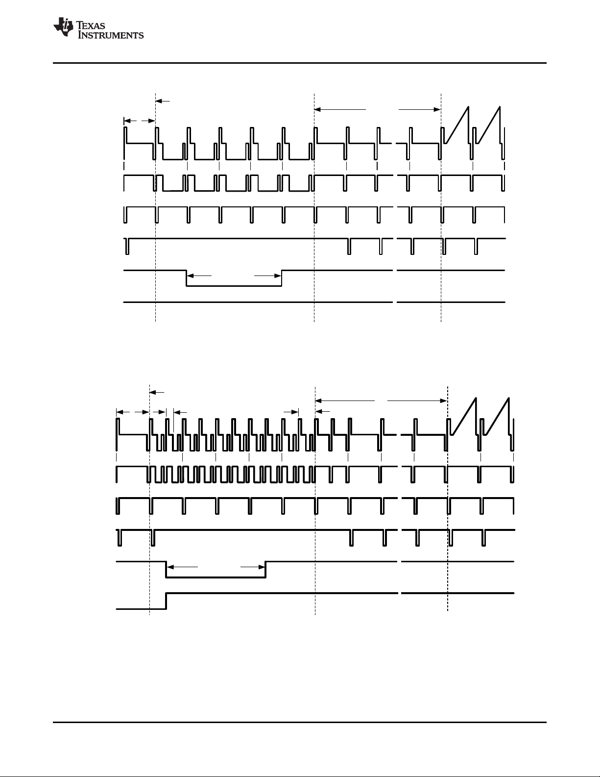
Figure 5. 480P Vertical Interval
Product Folder Links: LMH1980
1
V
IN
CSOUT
HSOUT
BPOUT
VSOUT
OEOUT
3 4 5 6 7 20 21 22
1125
FIELD 1
2
VERTICAL
SYNC SERRATION
T
VSOUT
= 3H
|
|
|
||
|
H
15H
LINE #
½ H
START OF FIELD 1
1
V
IN
CSOUT
HSOUT
BPOUT
VSOUT
OEOUT
3 4 5 6 7
25
(41)26(42)
27
(43)
750
(1125)
OEOUT LOGIC HIGH FOR
PROGRESSIVE VIDEO FORMATS
2
T
VSOUT
= 3H
|
|
||
|
H
20H (36H)
LINE #
START OF FRAME
|
8...
LMH1980
www.ti.com
HDTV Vertical Interval Timing Diagram (720P, 1080P)
Figure 6. 720P (1080P) Vertical Interval
SNLS263A –JULY 2007–REVISED MARCH 2013
HDTV Vertical Interval Timing Diagrams (1080I)
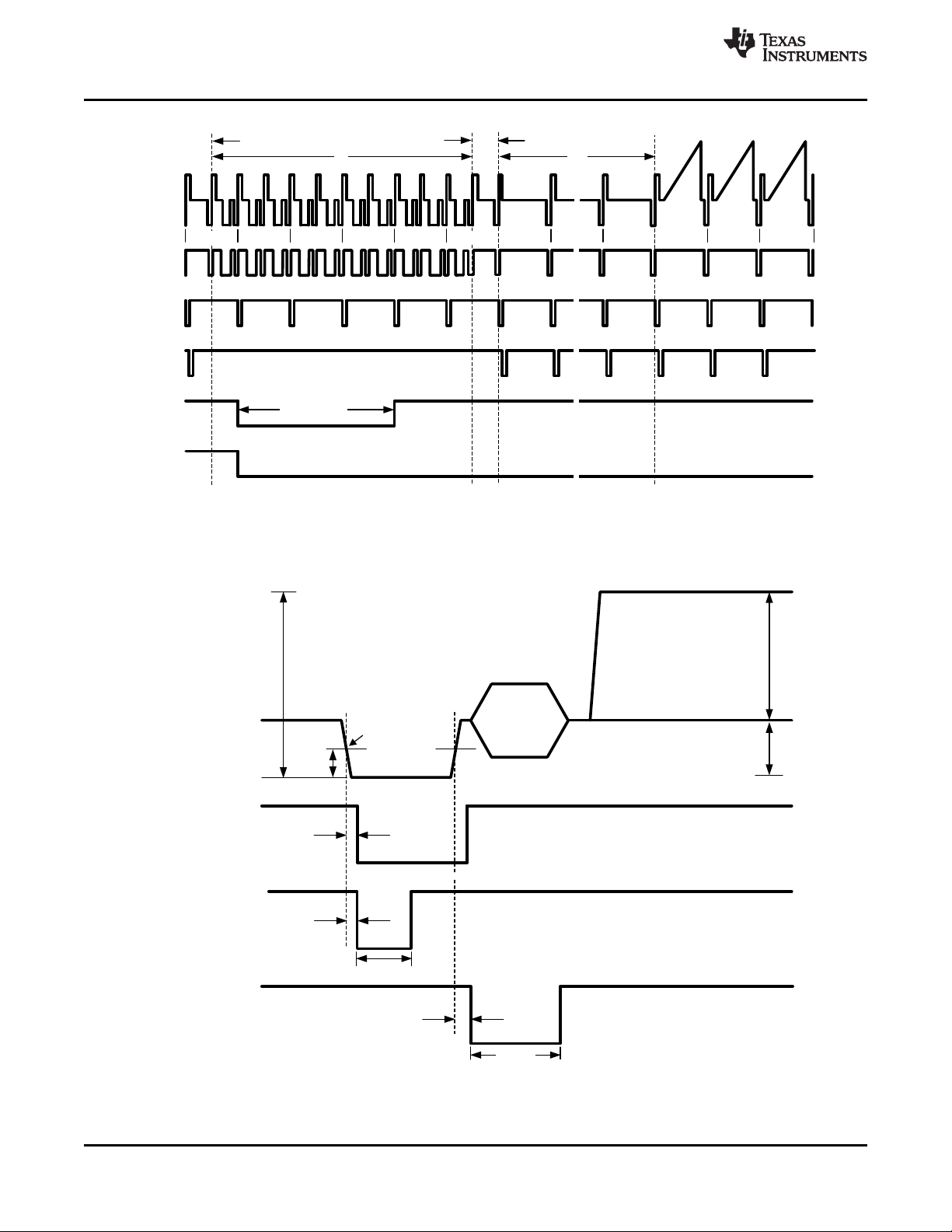
Figure 7. 1080I Field 1 Vertical Interval
Copyright © 2007–2013, Texas Instruments Incorporated Submit Documentation Feedback 7
Product Folder Links: LMH1980
V
IN
CSOUT
HSOUT
BPOUT
SYNC TIP LEVEL
BLANKING LEVEL
WHITE LEVEL
VIDEO
SYNC
50%
T
HSOUT
td
BPOUT
td
HSOUT
td
CSOUT
0.5 VPP to 2 V
PP
1 VPP (typ.)
T
BPOUT
VIDEO INPUT RANGE
O
H
NTSC/PAL
COLOR BURST
ENVELOPE
563
V
IN
CSOUT
HSOUT
BPOUT
VSOUT
OEOUT
565 566 567 568 569 583 584 585564 586LINE #
FIELD 2
15H5H
START OF FIELD 2
|
T
VSOUT
= 3H
|
| | | |
½ H
570...
LMH1980
SNLS263A –JULY 2007–REVISED MARCH 2013
www.ti.com
Figure 8. 1080I Field 2 Vertical Interval
SD/EDTV Horizontal Interval Timing Diagram
8 Submit Documentation Feedback Copyright © 2007–2013, Texas Instruments Incorporated
Figure 9. SD/EDTV Horizontal Interval with Bi-level Sync
Product Folder Links: LMH1980
 Loading...