

Page 1

User's Guide
SNVU637–October 2018
Using the LMG3411EVM-029 Half-Bridge and LMG34XX-
BB-EVM Breakout Board EVM
The LMG3411EVM-029 features two LMG3411R070 600V/12A GaN power transistors with integrated
drivers that are configured in a half bridge with all the required bias circuit and logic/power level shifting.
Essential power stage and gate driving high frequency current loops are fully enclosed on the board to
minimize parasitic inductances, reducing voltage overshoots and improving performance. The
LMG3411EVM-029 is configured to have a socket style external connection for easy interface with
external power stages to run the LMG3411R070 in various applications.
Contents
1 LMG3411EVM-029 User's Guide General TI High Voltage Evaluation User Safety Guidelines.................. 2
2 Description.................................................................................................................... 4
3 Schematic..................................................................................................................... 8
4 Test Setup................................................................................................................... 11
5 Test Procedure ............................................................................................................. 14
6 Typical Characteristics..................................................................................................... 15
7 EVM Assembly Drawing and PCB Layout .............................................................................. 17
8 Bill of Materials ............................................................................................................. 18
List of Figures
1 Simplified LMG3411EVM-029 Schematic ................................................................................ 5
2 Front and Back Side Photos of LMG3411EVM-029 .................................................................... 6
3 LMG3411EVM-029 Schematic............................................................................................. 8
4 Recommended Footprint for LMG3411EVM-029........................................................................ 9
5 LMG34XX-BB-EVM Schematic .......................................................................................... 10
6 LMG3411EVM-029 Connected with LMG34XX-BB-EVM ............................................................ 11
7 Recommended Connection Points....................................................................................... 12
8 Recommended Probe Connection for Logic Signals .................................................................. 15
9 Recommended Probe Connection for High Voltage Switch Node................................................... 15
10 Recommended Configuration for Heat Sink and Fan ................................................................. 15
11 Switching Waveforms with 480V input, 100kHz, 30% duty cycle, 6A output....................................... 15
12 Low to High Transition Waveform with 480V input, 100kHz, 30% duty cycle, 6A output ........................ 15
13 High to Low Transition Waveform with 480V input, 100kHz, 30% duty cycle, 6A output ........................ 15
14 LMG3411EVM-029 Top Layer and Components ...................................................................... 17
15 LMG3411EVM-029 Inner Copper Layer 1 .............................................................................. 17
16 LMG3411EVM-029 Inner Copper Layer 2 .............................................................................. 17
17 LMG3411EVM-029 Bottom Layer and Components .................................................................. 17
18 LMG34XX-BB-EVM Top Layer and Components...................................................................... 17
19 LMG34XX-BB-EVM Bottom Layer and Components.................................................................. 17
List of Tables
1 Logic Pin Function Description............................................................................................. 4
2 Power Pin Function Description ........................................................................................... 4
3 Test Point Functional Description........................................................................................ 13
SNVU637–October 2018
Submit Documentation Feedback
Using the LMG3411EVM-029 Half-Bridge and LMG34XX-BB-EVM Breakout
Copyright © 2018, Texas Instruments Incorporated
Board EVM
1
Page 2

WARNING
LMG3411EVM-029 User's Guide General TI High Voltage Evaluation User Safety Guidelines
4 List of Terminals............................................................................................................ 13
5 LMG3411EVM-029 List of Materials..................................................................................... 18
6 LMG34XX-BB-EVM List of Materials .................................................................................... 20
Trademarks
All trademarks are the property of their respective owners.
1 LMG3411EVM-029 User's Guide
General TI High Voltage Evaluation User Safety Guidelines
Always follow TI’s set-up and application instructions, including use of all interface components within their
recommended electrical rated voltage and power limits. Always use electrical safety precautions to help
ensure your personal safety and the safety of those working around you. Contact TI’s Product Information
Center http://support/ti./com for further information.
Save all warnings and instructions for future reference.
Failure to follow warnings and instructions may result in personal injury, property damage, or
death due to electrical shock and/or burn hazards.
The term TI HV EVM refers to an electronic device typically provided as an open framed, unenclosed
printed circuit board assembly. It is intended strictly for use in development laboratory environments,
solely for qualified professional users having training, expertise, and knowledge of electrical safety risks in
development and application of high-voltage electrical circuits. Any other use and/or application are strictly
prohibited by Texas Instruments. If you are not suitably qualified, you should immediately stop from further
use of the HV EVM.
• Work Area Safety:
– Maintain a clean and orderly work area .
– Qualified observer(s) must be present anytime circuits are energized.
– Effective barriers and signage must be present in the area where the TI HV EVM and its interface
electronics are energized, indicating operation of accessible high voltages may be present, for the
purpose of protecting inadvertent access.
– All interface circuits, power supplies, evaluation modules, instruments, meters, scopes and other
related apparatus used in a development environment exceeding 50 V
electrically located within a protected Emergency Power Off (EPO) protected power strip.
– Use a stable and non-conductive work surface.
– Use adequately insulated clamps and wires to attach measurement probes and instruments. No
freehand testing whenever possible.
• Electrical Safety:
As a precautionary measure, it is always a good engineering practice to assume that the entire
EVM may have fully accessible and active high voltages.
– De-energize the TI HV EVM and all its inputs, outputs, and electrical loads before performing any
electrical or other diagnostic measurements. Confirm that TI HV EVM power has been safely deenergized.
– With the EVM confirmed de-energized, proceed with required electrical circuit configurations, wiring,
measurement equipment hook-ups and other application needs, while still assuming the EVM circuit
and measuring instruments are electrically live.
– When EVM readiness is complete, energize the EVM as intended.
/75 VDC must be
RMS
www.ti.com
WARNING: While the EVM is energized, never touch the EVM or its electrical circuits as they
could be at high voltages capable of causing electrical shock hazard.
2
Using the LMG3411EVM-029 Half-Bridge and LMG34XX-BB-EVM Breakout
Board EVM
Copyright © 2018, Texas Instruments Incorporated
SNVU637–October 2018
Submit Documentation Feedback
Page 3
!
www.ti.com
• Personal Safety:
• Limitation for Safe Use:
Safety and Precautions
The EVM is designed for professionals who have received the appropriate technical training, and is
designed to operate from an AC power supply or a high-voltage DC supply. Please read this user guide
and the safety-related documents that come with the EVM package before operating this EVM.
LMG3411EVM-029 User's Guide General TI High Voltage Evaluation User Safety Guidelines
– Wear personal protective equipment, for example, latex gloves and/or safety glasses with side
shields or protect EVM in an adequate lucent plastic box with interlocks from accidental touch.
– EVMs are not to be used as all or part of a production unit.
CAUTION
Do not leave the EVM powered when unattended.
WARNING
Hot surface! Contact may cause burns. Do not touch!
WARNING
High Voltage! Electric shock is possible when connecting board to
live wire. Board should be handled with care by a professional.
For safety, use of isolated test equipment with overvoltage and
overcurrent protection is highly recommended.
SNVU637–October 2018
Submit Documentation Feedback
Copyright © 2018, Texas Instruments Incorporated
Using the LMG3411EVM-029 Half-Bridge and LMG34XX-BB-EVM Breakout
Board EVM
3
Page 4

Description
2 Description
The LMG3411EVM-029 operates as a daughter card as part of a larger custom designed system or with
the LMG34XX-BB-EVM breakout motherboard.
2.1 LMG3411EVM-029
The LMG3411EVM-029 configures two LMG3411R070 GaN FETs in a half bridge. All the bias and level
shifting components are included, allowing low side referenced signals to control both FETs. High
frequency bypass capacitors are included on the power stage in an optimized layout to minimize parasitic
inductance and reduce voltage overshoot.
There are 6 logic pins on the FET card.
Pin Description
AGND Logic and bias power ground return pin. Functionally isolated from PGND.
12V Auxiliary power input for when the LMG3410-HB-EVM is configured in bootstrap mode. Pin is not used
5V Auxiliary power input for the LMG3410-HB-EVM. Used to power logic isolators. Used as input bias power
FAULT Logic AND output from FAULT signal from LMG3410. Pin is either pulled to AGND or 5V.
Q2 Gate AGND referenced logic gate signal input for bottom LMG3410. Compatible with both 3.3V and 5V logic.
Q1 Gate AGND referenced logic gate signal input for top LMG3410. Compatible with both 3.3V and 5V logic.
www.ti.com
Table 1. Logic Pin Function Description
when configured in isolated power mode.
of LMG3410 devices when configured in isolated power mode.
There are 3 power pins on the FET card.
Table 2. Power Pin Function Description
PIN DESCRIPTION
VSW Switch node of the half bridge
VDC Input DC voltage of the half bridge
PGND Power ground of the half bridge. Functionally isolated from
AGND.
4
Using the LMG3411EVM-029 Half-Bridge and LMG34XX-BB-EVM Breakout
Board EVM
Copyright © 2018, Texas Instruments Incorporated
SNVU637–October 2018
Submit Documentation Feedback
Page 5

VDC
PGND
VSW
Q1 Gate
Q2 Gate
FAULT
IN
FAULT
IN
FAULT
D
S
D
S
www.ti.com
Description
Figure 1. Simplified LMG3411EVM-029 Schematic
2.1.1 FAULT
2.1.2 Power Pins
CAUTION
High-voltage levels are present on the evaluation module whenever it is
energized. Proper precautions must be taken when working with the EVM.
The FAULT pin of LMG3411EVM-029 is active low when an under voltage lockout on an auxiliary voltage
rail, over temperature or overcurrent event occurs on the LMG3411R070. The FAULT signal for both
LMG3411R070 devices are level shifted to AGND, where they are logic AND connected to the FAULT pin.
CAUTION
Please do NOT ignore FAULT signal when using LMG3411EVM-029. Turn off
both top and bottom devices, if any device is generating FAULT signal. The
device under fault condition may operate in undesired 3rd-quadrant mode and
may be over heated and damaged due to the high source-drain voltage drop if
the other device is still switching.
While there are some power stage bypass capacitors on the LMG3411EVM-029 from VDC to PGND to
minimize voltage overshoot during switching, more bulk capacitance is required to hold up the DC voltage
during operation. It is highly recommended to minimize, and ideally prevent, any overlap and parasitic
capacitance from VSW to VDC, PGND and any logic pins. The two grounds PGND and AGND are
functionally isolated from each other on the LMG3411EVM-029.
SNVU637–October 2018
Submit Documentation Feedback
Using the LMG3411EVM-029 Half-Bridge and LMG34XX-BB-EVM Breakout
Copyright © 2018, Texas Instruments Incorporated
Board EVM
5
Page 6
Description
2.1.3 Bootstrap Mode
The LMG3411EVM-029 card can be modified to operate in bootstrap mode, where the 12V bias voltage is
used to power both LMG3411R070 devices. This can be achieved by removing U4, U5 and R1, and
placing a 20 Ω resistor on R2, a 0 Ω resistor on R7 and a 600V SOD-123 diode on D1, such as Micro
Commercial Components UFM15PL-TP. Do NOT power up the LMG3411EVM-029 when R1, R2, R7, D1,
U4 and U5 are all populated.
2.1.4 Heat Sink
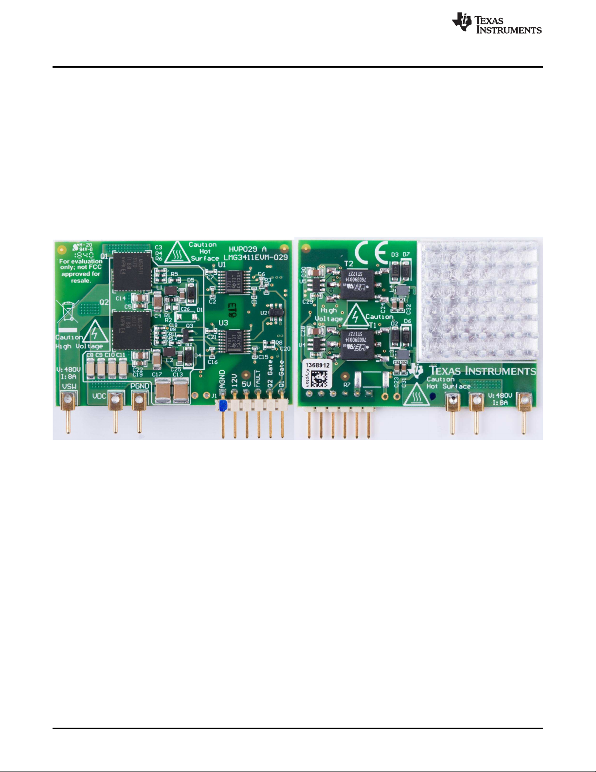
Heat sink is installed to help with heat dissipation of the LMG3411R070. Exposed copper pads that are
attached to the die attach pad (DAP) of both the high and low side devices are provided for a low thermal
impedance point to a heat sink. The two copper pads have high voltage potential difference between them
so an electrically isolative thermal interface material (TIM) is required. Bergquist BP100-0.005-00-1112
double sided adhesive tape TIM and Cool Innovations 3-101004U heat sink are recommended.
www.ti.com
Figure 2. Front and Back Side Photos of LMG3411EVM-029
2.2 LMG34XX-BB-EVM
To allow for quick operation the LMG34XX-BB-EVM is available to interface with the LMG3411EVM-029.
This mother board is designed to operate the LMG3411R070 as a synchronous open loop buck converter.
Easy probe locations are provided for measurement of logic and power stage voltages.
2.2.1 Bias Supply
The motherboard requires one 12V bias supply. A linear drop off regulator steps the voltage down to a
tightly regulated 5V for logic and auxiliary power of the LMG3411R070 when the LMG3410-HB-EVM is
configured in isolated power mode. When the LMG3411EVM-029 is configured in bootstrap mode the 12V
input is used to power the two LMG3411R070 devices.
2.2.2 Logic PWM Input
The LMG34XX-BB-EVM supports a single PWM, with complimentary signal and corresponding dead time
generated on board. A 0 V to 5 V magnitude input square wave is required. The complementary PWM
generation circuit creates 50 ns of dead time between both transitions of the PWM signals.
6
Using the LMG3411EVM-029 Half-Bridge and LMG34XX-BB-EVM Breakout
Board EVM
Copyright © 2018, Texas Instruments Incorporated
SNVU637–October 2018
Submit Documentation Feedback
Page 7

www.ti.com
2.2.3 Fault Protection
There is an option to disable PWM input to the FET card in the event of a fault signal from the
LMG3411EVM-029. When the FAULT Protect jumper is placed in the EN mode, PWM is disabled when
either LMG3411R070 has an active fault. This disable is not latching, so when the fault clears PWM
immediately resumes. If FAULT Protect mode is not desired it can be disabled by placing the jumper in
the DIS position. Besides, it is noted that to correctly observe the cycle-by-cycle overcurrent protection
with LMG34XX-BB-EVM, the jumper needs to be configured at DIS position. For the details of the over
current protection, please refer datasheet of LMG3411R070. The FAULT LED will still illuminate when
either LMG3410 has an active fault, regardless of the position of FAULT Protect jumper.
2.3 Typical Applications
The LMG3411EVM-029 is designed for use in AC/DC, DC/DC and DC/AC applications
• Totem-Pole PFC converters
• Phase-Shifted Full Bridge or LLC Converter
• Buck converter such as the LMG34XX-BB-EVM
2.4 Features
The LMG3411EVM-029 has the following features and specifications:
• Two options to bias the LMG3411R070, isolated power or from bootstrap diode
• Over temperature, cycle-by-cycle overcurrent, and under voltage lockout protection with FAULT
indication that is level shifted to an AGND referenced signal
• Gate logic input support of either 3.3V or 5V logic
• Maximum recommended operating voltage of 480V and absolute maximum voltage of 600V
The LMG34XX-BB-EVM has the following features and specifications:
• Requires only a single 12V bias supply
• Requires only a single 0V to 5V PWM input to generate gate drive signal
• PWM disable in the event of a fault from the LMG3411EVM-029
• Maximum recommended operating voltage of 480V and absolute maximum voltage of 600V
• Maximum recommended operating inductor current of 8A
Description
SNVU637–October 2018
Submit Documentation Feedback
Using the LMG3411EVM-029 Half-Bridge and LMG34XX-BB-EVM Breakout
Copyright © 2018, Texas Instruments Incorporated
Board EVM
7
Page 8
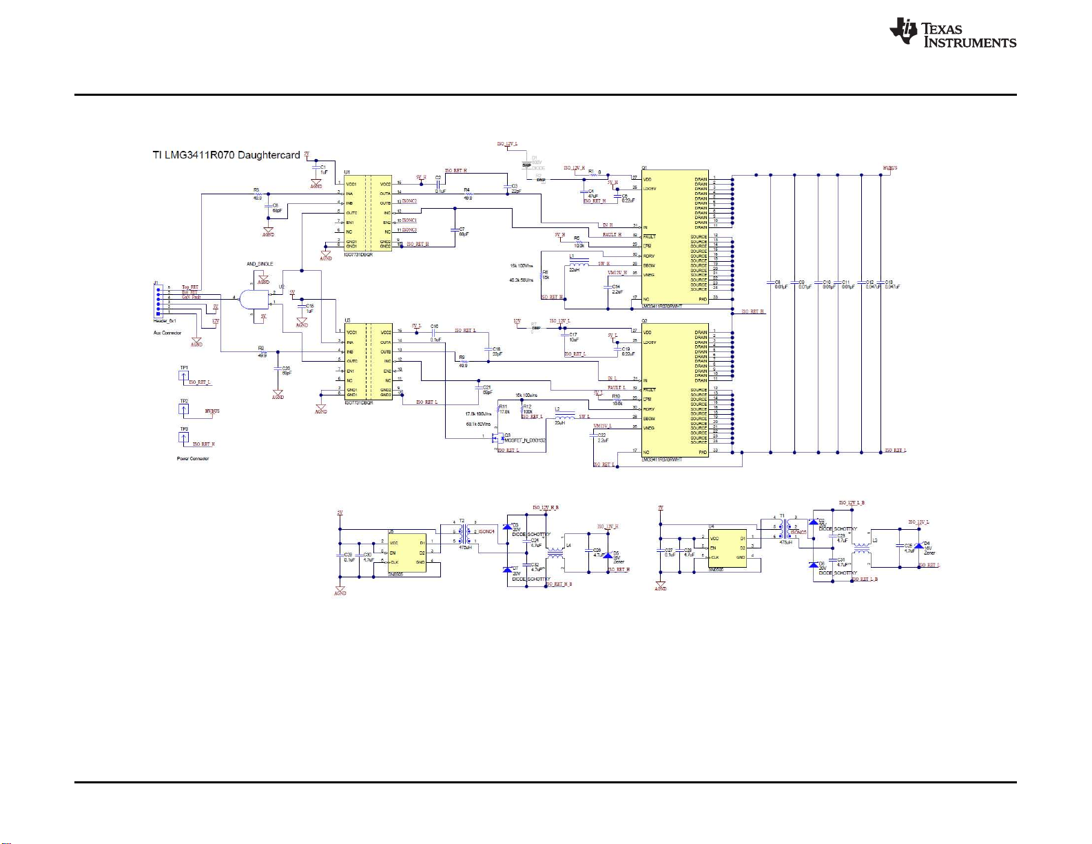
Schematic
3 Schematic
www.ti.com
8
Using the LMG3411EVM-029 Half-Bridge and LMG34XX-BB-EVM Breakout
Board EVM
Figure 3. LMG3411EVM-029 Schematic
SNVU637–October 2018
Submit Documentation Feedback
Copyright © 2018, Texas Instruments Incorporated
Page 9

www.ti.com
Schematic
SNVU637–October 2018
Submit Documentation Feedback
Figure 4. Recommended Footprint for LMG3411EVM-029
Using the LMG3411EVM-029 Half-Bridge and LMG34XX-BB-EVM Breakout
Copyright © 2018, Texas Instruments Incorporated
Board EVM
9
Page 10

AGND
1
234
5
J3
112404
AGND
1 6
5
2
U1A
SN74LVC2G14DCKR
1µF
C9
AGND
5V
39pF
C13
D2
BAT54WS-7-F
AGND
AGND
HDEAD1
PWM
1µF
C11
5V
3 4
5
2
U3B
SN74LVC2G14DCKR
39pF
C5
D1
BAT54WS-7-F
AGND
AGND
5V
LDEAD1
1µF
C4
5V
AGND
1.20k
R1
1.20k
R5
HVIN
PGND1
Vin
HVOUT
PGND2
Vout
LOW
HIGH
FAULT
1000pF
C14
AGND
PGND
1µF
C6
1
2
7
4
8
U2A
SN74LVC2G08IDCTRQ1
5
6
3
4
8
U2B
SN74LVC2G08IDCTRQ1
5V
AGND
5V
5V
5V
12V aux
FAULT Indicator
SW1 PGND3
AGND
0
R9
1
2
J6
282834-2
5µF
C1
5µF
C15
HIGH
LOW
PGND
PGND
PGND PGND
39pF
C7
0
R2
AGND
0
R4
39pF
C12
AGND
39pF
C10
AGND
0
R3
VDC
PGND
SW
AGND
5V
1 6
5
2
U3A
SN74LVC2G14DCKR
0.1µF
630V
C3
0.1µF
630V
C2
0.1µF
630V
C17
0.1µF
630V
C16
1µF
C18
AGND
1µF
C20
LOW_2
HIGH_2
HIGH_2
LOW_2
5
4
1
2
3
6
J4
TSW-106-07-G-S
1µF
C8
VAUX
ACMGND
1
2
3
4
5
6
J2
0448120024
AGND1
AGND4
5V
AGND
3 4
5
2
U1B
SN74LVC2G14DCKR
AGND3
0
R23
0
R21
IN1OUT
3
GND
2
TAB
4
U4
LM2940IMP-5.0/NOPB
33µF
C19
10µF
C21
12V
12V
12V
Green
1
2
D4
Red
1
2
D3
1.6k
R6
1.6k
R8
30k
R10
30k
R16
30k
R11
30k
R17
30k
R18
30k
R12
30k
R13
30k
R19
30k
R20
30k
R14
1
2
3
J7
TSW-103-07-G-S
5V
Red
1
2
D5
PGND
SH-J1
1
2
J5
282841-2
1
2
J1
282841-2
1
2
3
4
47µH
L3
DRQ73-470-R
TI HV Synchronous Buck Motherboard
150µH
L1
150µH
L2
10.0k
R7
5V
AGND
AGND
AGND
AGND2
Copyright © 2016, Texas Instruments Incorporated
Schematic
www.ti.com
10
Using the LMG3411EVM-029 Half-Bridge and LMG34XX-BB-EVM Breakout
Board EVM
Figure 5. LMG34XX-BB-EVM Schematic
Copyright © 2018, Texas Instruments Incorporated
Submit Documentation Feedback
SNVU637–October 2018
Page 11

www.ti.com
4 Test Setup
4.1 Test Equipment
DC Voltage Source: Capable of supplying the input of the EVM up to 480 V
DC Bias Source: Capable of 12 V output at up to 0.7 A
Function Generator: Capable of 0 V to 5 V square wave output with adjustable duty cycle and frequency in
desired operating range. It is recommended to operate the LMG3411EVM-029 and LMG34XX-BB-EVM
with a switching frequency between 50 kHz to 200 kHz.
Oscilloscope: Capable of at least 200 MHz operation. A 1 GHz or greater oscilloscope and probes with
short ground springs are recommended for accurate measurements.
DC Multimeter(s): Capable of 600 V measurement, suitable for determining operation and efficiency (if
desired).
DC Load: Capable of 600 V operation at up to 8 A in current-mode operation.
Fan: 200 LFM minimum airflow is recommended.
4.2 Recommended Test Setup
The LMG3411EVM-029 connects to the LMG34XX-BB-EVM as Figure 6 shows.
Test Setup
Figure 6. LMG3411EVM-029 Connected with LMG34XX-BB-EVM
The LMG3411EVM-029 power and probe connection points are shown in Figure 7.
SNVU637–October 2018
Submit Documentation Feedback
Using the LMG3411EVM-029 Half-Bridge and LMG34XX-BB-EVM Breakout
Copyright © 2018, Texas Instruments Incorporated
Board EVM
11
Page 12

Test Setup
www.ti.com
PCB Notes:
• Probe points for gate drive logic
• 100 mil header for PWM input, PWM signals to LMG3411EVM-029 and FAULT output
• BNC connector for PWM input
• 12V bias supply input
• FAULT Protection option header
• Power stage high voltage input
• Probe point for power stage switch node
• Power stage high voltage output
There are very high voltages present on the EVM. Some
components reach temperatures above 50°C. Precautions must be
taken when handling the board.
4.3 List of Test Points
Key test points on this EVM have been designed for use with oscilloscope probes with short ground
springs. Using the short ground spring instead of the alligator ground lead will minimize measurement
error and produce a cleaner signal with the fast switching GaN devices used on this EVM. The data
shown in this user guide has been obtained using such a measurement method.
Figure 7. Recommended Connection Points
WARNING
12
Using the LMG3411EVM-029 Half-Bridge and LMG34XX-BB-EVM Breakout
Board EVM
Copyright © 2018, Texas Instruments Incorporated
SNVU637–October 2018
Submit Documentation Feedback
Page 13

www.ti.com
Test Setup
Table 3. Test Point Functional Description
NAME DESCRIPTION
VAUX 12 V bias input connection before filter
ACMGND Ground for 12 V bias input before filter
5V 5 V bias
AGND1 Analog ground for logic
PWM Single input PWM signal
LDEAD1 Low side PWM signal before dead time generation
AGND3 Analog ground for logic
HDEAD1 High side PWM signal before dead time generation
AGND4 Analog ground for logic
LOW Low side PWM signal with dead time
HIGH High side PWM signal with dead time
AGND2 Analog ground for logic
12V 12 V bias after filter
PGND1 Power ground
HVIN DC input voltage
PGND2 Power ground
HVOUT DC output voltage
PGND3 Power ground
SW1 Switch node voltage
4.4 List of Terminals
TERMINAL NAME DESCRIPTION
J1 VIN Input DC voltage input
J5 VOUT Output DC voltage output
J6 12V AUX 12 V bias voltage input
J3 PWM INPUT Single 0 V to 5 V PWM input for gate
J4 LOGIC Header to connect PWM, FAULT logic
J2 HB Card PIN Connector to interface LMG3411EVM-029
Table 4. List of Terminals
board
SNVU637–October 2018
Submit Documentation Feedback
Using the LMG3411EVM-029 Half-Bridge and LMG34XX-BB-EVM Breakout
Copyright © 2018, Texas Instruments Incorporated
Board EVM
13
Page 14

Test Procedure
5 Test Procedure
5.1 Setup
The following procedure is recommended to set up the LMG34XX-BB-EVM with the LMG3411EVM-029:
• Connect LMG3411EVM-029 to LMG34XX-BB-EVM
• Connect oscilloscope or multimeter probes to desired test points as shown in A or G
• Connect the 12 V bias supply, load to the output, and input supply to the input
• Connect the function generator to either the BNC connector PWM input at C or 100 mil header
connector input at pin 6 (PWM) and pin 5 (GND) at B.
• Enable an external fan to direct airflow across the heat sink attached to the LMG3411EVM-029
5.2 Startup and Operating Procedure
The following procedure is recommended to enable the LMG34XX-BB-EVM with the LMG3411EVM-029:
1. Power up the 12 V bias supply. Ensure the top right green “Aux Enable” LED is illuminated.
2. Enable PWM on the function generator
3. Power up high voltage input supply. Ensure the red “HV Enable” LED is illuminated when the input
supply is above 20 V.
www.ti.com
WARNING
Do NOT turn on device at absolute maximum voltage. It is
recommended to start at voltages at or below 480 V, and then
increase the input voltage slowly while monitoring VSWto insure the
peak voltage does not exceed the absolute maximum rating of 600
V.
5.3 Shutdown Procedure
1. Turn off input supply then PWM. Wait until red “HV Enable” LED turns off.
2. Disable 12 V bias supply.
5.4 Additional Operation Notes
• Fault protection on the LMG34XX-BB-EVM is not latching, so if a fault clears and the LMG34XX-BB-
EVM is still operational PWM will resume.
14
Using the LMG3411EVM-029 Half-Bridge and LMG34XX-BB-EVM Breakout
Board EVM
Copyright © 2018, Texas Instruments Incorporated
SNVU637–October 2018
Submit Documentation Feedback
Page 15

www.ti.com
6 Typical Characteristics
Typical Characteristics
Figure 8. Recommended Probe Connection for Logic
Signals
Figure 9. Recommended Probe Connection for High
Voltage Switch Node
SNVU637–October 2018
Submit Documentation Feedback
Using the LMG3411EVM-029 Half-Bridge and LMG34XX-BB-EVM Breakout
Copyright © 2018, Texas Instruments Incorporated
Board EVM
15
Page 16

Typical Characteristics
www.ti.com
Figure 11. Switching Waveforms with 480V input, 100kHz,
30% duty cycle, 6A output
Figure 10. Recommended Configuration for Heat Sink and
Fan
Figure 12. Low to High Transition Waveform with 480V
input, 100kHz, 30% duty cycle, 6A output
Figure 13. High to Low Transition Waveform with 480V
input, 100kHz, 30% duty cycle, 6A output
16
Using the LMG3411EVM-029 Half-Bridge and LMG34XX-BB-EVM Breakout
Board EVM
Copyright © 2018, Texas Instruments Incorporated
SNVU637–October 2018
Submit Documentation Feedback
Page 17

www.ti.com
7 EVM Assembly Drawing and PCB Layout
EVM Assembly Drawing and PCB Layout
Figure 14. LMG3411EVM-029 Top Layer and Components
Figure 16. LMG3411EVM-029 Inner Copper Layer 2
Figure 15. LMG3411EVM-029 Inner Copper Layer 1
Figure 17. LMG3411EVM-029 Bottom Layer and
Components
Figure 18. LMG34XX-BB-EVM Top Layer and Components Figure 19. LMG34XX-BB-EVM Bottom Layer and
Components
SNVU637–October 2018
Submit Documentation Feedback
Copyright © 2018, Texas Instruments Incorporated
Using the LMG3411EVM-029 Half-Bridge and LMG34XX-BB-EVM Breakout
Board EVM
17
Page 18

Bill of Materials
8 Bill of Materials
QTY DESIGNATOR DESCRIPTION PART NUMBER MANUFACTURER
2 C1, C15 CAP, CERM, 1 µF, 16 V, +/- 10%, X5R,
4 C6, C7, C20, C21 CAP, CERM, 68 pF, 50 V, +/- 5%,
4 C2, C16, C27, C29 CAP, CERM, 0.1 µF, 50 V, +/- 10%, X7R,
2 C3, C18 CAP, CERM, 22 pF, 50 V, +/- 5%,
2 C5, C19 CAP, CERM, 0.22 µF, 50 V, +/- 10%, X7R,
1 C4 CAP, CERM, 47 µF, 25 V, +/- 20%, X5R,
2 C14, C22 CAP, CERM, 2.2uF, 25V, +/-10%, X7R,
4 C8, C9, C10, C11 CAP, CERM, 0.01uF, 1000V, +/-10%, X7R,
2 C12, C13 CAP, CERM, 0.047 µF, 1000 V, +/- 10%,
6 C23, C24, C25, C26,
C31, C32
1 C17 CAP, CERM, 10 µF, 25 V, +/- 10%, X7R,
2 C28, C30 CAP, CERM, 4.7 µF, 16 V, +/- 10%, X7R,
4 D2, D3, D6, D7 Diode, Schottky, 20 V, 0.5 A, SOD-123 MBR0520LT1G ON Semiconductor
2 D4, D5 Diode, Zener, 16 V, 500 mW, SOD-123 MMSZ4703T1G ON Semiconductor
1 H2 'Cool Innovations Heat sink 1.00''x1.00'' 3-101004U Cool Innovations
1 J1 Header, 2.54mm, 6x1, Gold, R/A, TH 90121-0766 Molex
2 L1, L2 Inductor, Wirewound, 22 µH, 0.49 A, 0.56
2 L3, L4 Coupled inductor, 0.2 A, 0.45 ohm, SMD ACM2520-601-2P-T002 TDK
2 Q1, Q2 600-V 70mohm GaN With Integrated Driver
1 Q3 MOSFET, N-CH, 20 V, 0.75 A, SOT-23 MGSF1N02LT1G ON Semiconductor
1 R1 RES, 0, 5%, 0.1 W, 0603 CRCW06030000Z0EA Vishay-Dale
4 R3, R4, R8, R19 RES, 49.9, 1%, 0.063 W, 0402 RC0402FR-0749R9L Yageo America
1 R6 RES, 15 k, 5%, 0.063 W, 0402 CRCW040215K0JNED Vishay-Dale
1 R611 RES, 17.8 k, 1%, 0.063 W, 0402 CRCW040217K8FKED Vishay-Dale
2 R5, R10 RES, 10.0 k, 1%, 0.1 W, 0402 ERJ-2RKF1002X Panasonic
1 R12 RES, 100 k, 1%, 0.063 W, 0402 RC1005F104CS Samsung Electro-
2 T1, T2 Transformer, 475uH, SMT 760390014 Wurth Elektronik
1 H1 'Bergquist double sided thermal tape 'TI-Bond Ply100
3 TP1, TP2, TP3 Edge-Mount Pin, Gold 3620-1-32-15-00-00-08-0 Mill-Max
2 U1, U3 High Speed, Robust EMC Reinforced Triple-
2 U4, U5 Low-Noise 1 A, 420 kHz Transformer Driver,
Table 5. LMG3411EVM-029 List of Materials
0402
C0G/NP0, 0402
0402
C0G/NP0, 0402
0603
1206_190
0805
1206
X7R, 1812
CAP, CERM, 4.7 µF, 35 V, +/- 10%, X5R,
0603
1206_190
AEC-Q200 Grade 1, 0805
ohm, SMD
and Cycle-by-cycle Overcurrent Protection,
RWH0032A (VQFN-32)
Channel Digital Isolator, DBQ0016A (SSOP-
16)
DBV0006A (SOT-6)
EMK105BJ105KVHF Taiyo Yuden
GRM1555C1H680JA01D MuRata
C1005X7R1H104K050BB TDK
C1005C0G1H220J050BA TDK
C1608X7R1H224K080AB TDK
C3216X5R1E476M160AC TDK
GRM21BR71E225KA73L MuRata
C1206X103KDRAC7800 Kemet
C1812V473KDRACTU Kemet
GRM188R6YA475KE15D MuRata
C1206C106K3RACTU Kemet
GCM21BR71C475KA73K MuRata
BRC2518T220K Taiyo Yuden
LMG3411R070RWHT Texas Instruments
0.005"/.127mm(1).cu-
27.0mm by 27.0mm
ISO7731DBQR Texas Instruments
SN6505BDBVR Texas Instruments
www.ti.com
Mechanics
Bergquist
18
Using the LMG3411EVM-029 Half-Bridge and LMG34XX-BB-EVM Breakout
Board EVM
Copyright © 2018, Texas Instruments Incorporated
SNVU637–October 2018
Submit Documentation Feedback
Page 19

www.ti.com
Bill of Materials
Table 5. LMG3411EVM-029 List of Materials (continued)
QTY DESIGNATOR DESCRIPTION PART NUMBER MANUFACTURER
1 U2 Single 2-Input Positive-AND Gate,
0 D1 Diode, Ultrafast, 600 V, 1 A, SOD-123FL UFM15PL-TP Micro Commercial
0 FID1, FID2, FID3, FID4,
FID5, FID6
0 R2 RES, 20, 5%, 0.1 W, AEC-Q200 Grade 0,
0 R7 RES, 0, 5%, 1 W, AEC-Q200 Grade 0, 2512 CRCW25120000Z0EG Vishay-Dale
DBV0005A
Fiducial mark. There is nothing to buy or
mount
0603
SN74AHC1G08DBVR Texas Instruments
Components
N/A N/A
CRCW060320R0JNEA Vishay-Dale
SNVU637–October 2018
Submit Documentation Feedback
Using the LMG3411EVM-029 Half-Bridge and LMG34XX-BB-EVM Breakout
Copyright © 2018, Texas Instruments Incorporated
Board EVM
19
Page 20

Bill of Materials
www.ti.com
Table 6. LMG34XX-BB-EVM List of Materials
QTY DESIGNATOR DESCRIPTION PART NUMBER MANUFACTURER
5 5V, 12V, HVIN, HVOUT,
VAUX
5 ACMGND, AGND1, AGND2,
PGND1, PGND2
2 C1, C15 CAP, Film, 5 µF, 1000 V, +/- 5%, 0.016 ohm,THMKP1848S55010JP2C Vishay-Components
Test Point, Compact, Red, TH 5005 Keystone
Test Point, Compact, Black, TH 5006 Keystone
4 C2, C3, C16, C17 CAP, CERM, 0.1uF, 630V, +/-10%, X7R,
1812
5 C4, C6, C8, C9, C11 CAP, CERM, 1 µF, 25 V, +/- 10%, X7R,
0603
2 C5, C13 CAP, CERM, 39 pF, 50 V, +/- 5%,
C0G/NP0, 0603
1 C14 CAP, CERM, 1000 pF, 25 V, +/- 5%,
C0G/NP0, 0603
2 C18, C20 CAP, CERM, 1 µF, 25 V, +/- 10%, X7R,
0603
1 C19 CAP, TA, 33 µF, 16 V, +/- 10%, 0.35 ohm,
SMD
1 C21 CAP, CERM, 10 µF, 25 V, +/- 10%, X5R,
0805
2 D1, D2 Diode, Schottky, 30 V, 0.2 A, SOD-323 BAT54WS-7-F Diodes Inc.
2 D3, D5 LED, Red, SMD LS L29K-G1J2-1-Z OSRAM
1 D4 LED, Green, SMD LG L29K-G2J1-24-Z OSRAM
6 H1, H2, H3, H4, H9, H10 Machine Screw, Round, #4-40 x 1/4, Nylon,
Philips panhead
6 H5, H6, H7, H8, H11, H12 Standoff, Hex, 0.5"L #4-40 Nylon 1902C Keystone
2 J1, J5 Terminal Block, 2x1, 5.08mm, TH 282841-2 TE Connectivity
1 J2 Receptacle, 2.54mm, 6x1, Gold, TH 448120024 Molex
1 J3 Connector, TH, BNC 112404 Amphenol Connex
1 J4 Header, 100mil, 6x1, Gold, TH TSW-106-07-G-S Samtec
1 J6 Terminal Block, 2x1, 2.54mm, TH 282834-2 TE Connectivity
1 J7 Header, 100mil, 3x1, Gold, TH TSW-103-07-G-S Samtec
2 L1, L2 Inductor, Toroid, 150 µH, 7.5 A, 0.05 ohm,TH2300HT-151-H-RC Bourns
GRM43DR72J104KW01L MuRata
C1608X7R1E105K080AB TDK
C1608C0G1H390J TDK
GRM1885C1E102JA01D MuRata
GRM188R71E105KA12D MuRata
TPSB336K016R0350 AVX
GRM219R61E106KA12D MuRata
NY PMS 440 0025 PH B and F Fastener Supply
1 L3 Coupled inductor, 47 µH, 1.14 A, 0.241 ohm,
3 PGND, SW, VDC Pin Receptacle, .032-.046" .075" Dia, Gold,TH0312-0-15-15-34-27-10-0 Mill-Max
2 R1, R5 RES, 1.20 k, 1%, 0.1 W, 0603 RC0603FR-071K2L Yageo America
6 R2, R3, R4, R9, R21, R23 RES, 0, 5%, 0.1 W, 0603 CRCW06030000Z0EA Vishay-Dale
2 R6, R8 RES, 1.6 k, 5%, 0.1 W, 0603 CRCW06031K60JNEA Vishay-Dale
1 R7 RES, 10.0 k, 1%, 0.1 W, 0603 ERJ-3EKF1002V Panasonic
10 R10, R11, R12, R13, R14,
R16, R17, R18, R19, R20
1 SH-J1 Shunt, 100mil, Gold plated, Black 969102-0000-DA 3M
2 U1, U3 Dual Schmitt-Trigger Inverter, DCK0006A SN74LVC2G14DCKR Texas Instruments
1 U2 DUAL 2-INPUT POSITIVE-AND GATE,
1 U4 1A Low Dropout Regulator, 4-pin SOT-223,
20
Using the LMG3411EVM-029 Half-Bridge and LMG34XX-BB-EVM Breakout
Board EVM
+/- 20%, SMD
RES, 30 k, 5%, 0.25 W, 1206 CRCW120630K0JNEA Vishay-Dale
DCT0008A
Pb-Free
Copyright © 2018, Texas Instruments Incorporated
DRQ73-470-R Cooper Bussman
SN74LVC2G08IDCTRQ1 Texas Instruments
LM2940IMP-5.0/NOPB Texas Instruments
SNVU637–October 2018
Submit Documentation Feedback
Page 21

STANDARD TERMS FOR EVALUATION MODULES
1. Delivery: TI delivers TI evaluation boards, kits, or modules, including any accompanying demonstration software, components, and/or
documentation which may be provided together or separately (collectively, an “EVM” or “EVMs”) to the User (“User”) in accordance
with the terms set forth herein. User's acceptance of the EVM is expressly subject to the following terms.
1.1 EVMs are intended solely for product or software developers for use in a research and development setting to facilitate feasibility
evaluation, experimentation, or scientific analysis of TI semiconductors products. EVMs have no direct function and are not
finished products. EVMs shall not be directly or indirectly assembled as a part or subassembly in any finished product. For
clarification, any software or software tools provided with the EVM (“Software”) shall not be subject to the terms and conditions
set forth herein but rather shall be subject to the applicable terms that accompany such Software
1.2 EVMs are not intended for consumer or household use. EVMs may not be sold, sublicensed, leased, rented, loaned, assigned,
or otherwise distributed for commercial purposes by Users, in whole or in part, or used in any finished product or production
system.
2 Limited Warranty and Related Remedies/Disclaimers:
2.1 These terms do not apply to Software. The warranty, if any, for Software is covered in the applicable Software License
Agreement.
2.2 TI warrants that the TI EVM will conform to TI's published specifications for ninety (90) days after the date TI delivers such EVM
to User. Notwithstanding the foregoing, TI shall not be liable for a nonconforming EVM if (a) the nonconformity was caused by
neglect, misuse or mistreatment by an entity other than TI, including improper installation or testing, or for any EVMs that have
been altered or modified in any way by an entity other than TI, (b) the nonconformity resulted from User's design, specifications
or instructions for such EVMs or improper system design, or (c) User has not paid on time. Testing and other quality control
techniques are used to the extent TI deems necessary. TI does not test all parameters of each EVM.
User's claims against TI under this Section 2 are void if User fails to notify TI of any apparent defects in the EVMs within ten (10)
business days after delivery, or of any hidden defects with ten (10) business days after the defect has been detected.
2.3 TI's sole liability shall be at its option to repair or replace EVMs that fail to conform to the warranty set forth above, or credit
User's account for such EVM. TI's liability under this warranty shall be limited to EVMs that are returned during the warranty
period to the address designated by TI and that are determined by TI not to conform to such warranty. If TI elects to repair or
replace such EVM, TI shall have a reasonable time to repair such EVM or provide replacements. Repaired EVMs shall be
warranted for the remainder of the original warranty period. Replaced EVMs shall be warranted for a new full ninety (90) day
warranty period.
3 Regulatory Notices:
3.1 United States
3.1.1 Notice applicable to EVMs not FCC-Approved:
FCC NOTICE: This kit is designed to allow product developers to evaluate electronic components, circuitry, or software
associated with the kit to determine whether to incorporate such items in a finished product and software developers to write
software applications for use with the end product. This kit is not a finished product and when assembled may not be resold or
otherwise marketed unless all required FCC equipment authorizations are first obtained. Operation is subject to the condition
that this product not cause harmful interference to licensed radio stations and that this product accept harmful interference.
Unless the assembled kit is designed to operate under part 15, part 18 or part 95 of this chapter, the operator of the kit must
operate under the authority of an FCC license holder or must secure an experimental authorization under part 5 of this chapter.
3.1.2 For EVMs annotated as FCC – FEDERAL COMMUNICATIONS COMMISSION Part 15 Compliant:
CAUTION
This device complies with part 15 of the FCC Rules. Operation is subject to the following two conditions: (1) This device may not
cause harmful interference, and (2) this device must accept any interference received, including interference that may cause
undesired operation.
Changes or modifications not expressly approved by the party responsible for compliance could void the user's authority to
operate the equipment.
FCC Interference Statement for Class A EVM devices
NOTE: This equipment has been tested and found to comply with the limits for a Class A digital device, pursuant to part 15 of
the FCC Rules. These limits are designed to provide reasonable protection against harmful interference when the equipment is
operated in a commercial environment. This equipment generates, uses, and can radiate radio frequency energy and, if not
installed and used in accordance with the instruction manual, may cause harmful interference to radio communications.
Operation of this equipment in a residential area is likely to cause harmful interference in which case the user will be required to
correct the interference at his own expense.
Page 22

FCC Interference Statement for Class B EVM devices
NOTE: This equipment has been tested and found to comply with the limits for a Class B digital device, pursuant to part 15 of
the FCC Rules. These limits are designed to provide reasonable protection against harmful interference in a residential
installation. This equipment generates, uses and can radiate radio frequency energy and, if not installed and used in accordance
with the instructions, may cause harmful interference to radio communications. However, there is no guarantee that interference
will not occur in a particular installation. If this equipment does cause harmful interference to radio or television reception, which
can be determined by turning the equipment off and on, the user is encouraged to try to correct the interference by one or more
of the following measures:
• Reorient or relocate the receiving antenna.
• Increase the separation between the equipment and receiver.
• Connect the equipment into an outlet on a circuit different from that to which the receiver is connected.
• Consult the dealer or an experienced radio/TV technician for help.
3.2 Canada
3.2.1 For EVMs issued with an Industry Canada Certificate of Conformance to RSS-210 or RSS-247
Concerning EVMs Including Radio Transmitters:
This device complies with Industry Canada license-exempt RSSs. Operation is subject to the following two conditions:
(1) this device may not cause interference, and (2) this device must accept any interference, including interference that may
cause undesired operation of the device.
Concernant les EVMs avec appareils radio:
Le présent appareil est conforme aux CNR d'Industrie Canada applicables aux appareils radio exempts de licence. L'exploitation
est autorisée aux deux conditions suivantes: (1) l'appareil ne doit pas produire de brouillage, et (2) l'utilisateur de l'appareil doit
accepter tout brouillage radioélectrique subi, même si le brouillage est susceptible d'en compromettre le fonctionnement.
Concerning EVMs Including Detachable Antennas:
Under Industry Canada regulations, this radio transmitter may only operate using an antenna of a type and maximum (or lesser)
gain approved for the transmitter by Industry Canada. To reduce potential radio interference to other users, the antenna type
and its gain should be so chosen that the equivalent isotropically radiated power (e.i.r.p.) is not more than that necessary for
successful communication. This radio transmitter has been approved by Industry Canada to operate with the antenna types
listed in the user guide with the maximum permissible gain and required antenna impedance for each antenna type indicated.
Antenna types not included in this list, having a gain greater than the maximum gain indicated for that type, are strictly prohibited
for use with this device.
Concernant les EVMs avec antennes détachables
Conformément à la réglementation d'Industrie Canada, le présent émetteur radio peut fonctionner avec une antenne d'un type et
d'un gain maximal (ou inférieur) approuvé pour l'émetteur par Industrie Canada. Dans le but de réduire les risques de brouillage
radioélectrique à l'intention des autres utilisateurs, il faut choisir le type d'antenne et son gain de sorte que la puissance isotrope
rayonnée équivalente (p.i.r.e.) ne dépasse pas l'intensité nécessaire à l'établissement d'une communication satisfaisante. Le
présent émetteur radio a été approuvé par Industrie Canada pour fonctionner avec les types d'antenne énumérés dans le
manuel d’usage et ayant un gain admissible maximal et l'impédance requise pour chaque type d'antenne. Les types d'antenne
non inclus dans cette liste, ou dont le gain est supérieur au gain maximal indiqué, sont strictement interdits pour l'exploitation de
l'émetteur
3.3 Japan
3.3.1 Notice for EVMs delivered in Japan: Please see http://www.tij.co.jp/lsds/ti_ja/general/eStore/notice_01.page 日本国内に
輸入される評価用キット、ボードについては、次のところをご覧ください。
http://www.tij.co.jp/lsds/ti_ja/general/eStore/notice_01.page
3.3.2 Notice for Users of EVMs Considered “Radio Frequency Products” in Japan: EVMs entering Japan may not be certified
by TI as conforming to Technical Regulations of Radio Law of Japan.
If User uses EVMs in Japan, not certified to Technical Regulations of Radio Law of Japan, User is required to follow the
instructions set forth by Radio Law of Japan, which includes, but is not limited to, the instructions below with respect to EVMs
(which for the avoidance of doubt are stated strictly for convenience and should be verified by User):
1. Use EVMs in a shielded room or any other test facility as defined in the notification #173 issued by Ministry of Internal
Affairs and Communications on March 28, 2006, based on Sub-section 1.1 of Article 6 of the Ministry’s Rule for
Enforcement of Radio Law of Japan,
2. Use EVMs only after User obtains the license of Test Radio Station as provided in Radio Law of Japan with respect to
EVMs, or
3. Use of EVMs only after User obtains the Technical Regulations Conformity Certification as provided in Radio Law of Japan
with respect to EVMs. Also, do not transfer EVMs, unless User gives the same notice above to the transferee. Please note
that if User does not follow the instructions above, User will be subject to penalties of Radio Law of Japan.
Page 23

【無線電波を送信する製品の開発キットをお使いになる際の注意事項】 開発キットの中には技術基準適合証明を受けて
いないものがあります。 技術適合証明を受けていないもののご使用に際しては、電波法遵守のため、以下のいずれかの
措置を取っていただく必要がありますのでご注意ください。
1. 電波法施行規則第6条第1項第1号に基づく平成18年3月28日総務省告示第173号で定められた電波暗室等の試験設備でご使用
いただく。
2. 実験局の免許を取得後ご使用いただく。
3. 技術基準適合証明を取得後ご使用いただく。
なお、本製品は、上記の「ご使用にあたっての注意」を譲渡先、移転先に通知しない限り、譲渡、移転できないものとします。
上記を遵守頂けない場合は、電波法の罰則が適用される可能性があることをご留意ください。 日本テキサス・イ
ンスツルメンツ株式会社
東京都新宿区西新宿6丁目24番1号
西新宿三井ビル
3.3.3 Notice for EVMs for Power Line Communication: Please see http://www.tij.co.jp/lsds/ti_ja/general/eStore/notice_02.page
電力線搬送波通信についての開発キットをお使いになる際の注意事項については、次のところをご覧ください。http:/
/www.tij.co.jp/lsds/ti_ja/general/eStore/notice_02.page
3.4 European Union
3.4.1 For EVMs subject to EU Directive 2014/30/EU (Electromagnetic Compatibility Directive):
This is a class A product intended for use in environments other than domestic environments that are connected to a
low-voltage power-supply network that supplies buildings used for domestic purposes. In a domestic environment this
product may cause radio interference in which case the user may be required to take adequate measures.
4 EVM Use Restrictions and Warnings:
4.1 EVMS ARE NOT FOR USE IN FUNCTIONAL SAFETY AND/OR SAFETY CRITICAL EVALUATIONS, INCLUDING BUT NOT
LIMITED TO EVALUATIONS OF LIFE SUPPORT APPLICATIONS.
4.2 User must read and apply the user guide and other available documentation provided by TI regarding the EVM prior to handling
or using the EVM, including without limitation any warning or restriction notices. The notices contain important safety information
related to, for example, temperatures and voltages.
4.3 Safety-Related Warnings and Restrictions:
4.3.1 User shall operate the EVM within TI’s recommended specifications and environmental considerations stated in the user
guide, other available documentation provided by TI, and any other applicable requirements and employ reasonable and
customary safeguards. Exceeding the specified performance ratings and specifications (including but not limited to input
and output voltage, current, power, and environmental ranges) for the EVM may cause personal injury or death, or
property damage. If there are questions concerning performance ratings and specifications, User should contact a TI
field representative prior to connecting interface electronics including input power and intended loads. Any loads applied
outside of the specified output range may also result in unintended and/or inaccurate operation and/or possible
permanent damage to the EVM and/or interface electronics. Please consult the EVM user guide prior to connecting any
load to the EVM output. If there is uncertainty as to the load specification, please contact a TI field representative.
During normal operation, even with the inputs and outputs kept within the specified allowable ranges, some circuit
components may have elevated case temperatures. These components include but are not limited to linear regulators,
switching transistors, pass transistors, current sense resistors, and heat sinks, which can be identified using the
information in the associated documentation. When working with the EVM, please be aware that the EVM may become
very warm.
4.3.2 EVMs are intended solely for use by technically qualified, professional electronics experts who are familiar with the
dangers and application risks associated with handling electrical mechanical components, systems, and subsystems.
User assumes all responsibility and liability for proper and safe handling and use of the EVM by User or its employees,
affiliates, contractors or designees. User assumes all responsibility and liability to ensure that any interfaces (electronic
and/or mechanical) between the EVM and any human body are designed with suitable isolation and means to safely
limit accessible leakage currents to minimize the risk of electrical shock hazard. User assumes all responsibility and
liability for any improper or unsafe handling or use of the EVM by User or its employees, affiliates, contractors or
designees.
4.4 User assumes all responsibility and liability to determine whether the EVM is subject to any applicable international, federal,
state, or local laws and regulations related to User’s handling and use of the EVM and, if applicable, User assumes all
responsibility and liability for compliance in all respects with such laws and regulations. User assumes all responsibility and
liability for proper disposal and recycling of the EVM consistent with all applicable international, federal, state, and local
requirements.
5. Accuracy of Information: To the extent TI provides information on the availability and function of EVMs, TI attempts to be as accurate
as possible. However, TI does not warrant the accuracy of EVM descriptions, EVM availability or other information on its websites as
accurate, complete, reliable, current, or error-free.
Page 24

6. Disclaimers:
6.1 EXCEPT AS SET FORTH ABOVE, EVMS AND ANY MATERIALS PROVIDED WITH THE EVM (INCLUDING, BUT NOT
LIMITED TO, REFERENCE DESIGNS AND THE DESIGN OF THE EVM ITSELF) ARE PROVIDED "AS IS" AND "WITH ALL
FAULTS." TI DISCLAIMS ALL OTHER WARRANTIES, EXPRESS OR IMPLIED, REGARDING SUCH ITEMS, INCLUDING BUT
NOT LIMITED TO ANY EPIDEMIC FAILURE WARRANTY OR IMPLIED WARRANTIES OF MERCHANTABILITY OR FITNESS
FOR A PARTICULAR PURPOSE OR NON-INFRINGEMENT OF ANY THIRD PARTY PATENTS, COPYRIGHTS, TRADE
SECRETS OR OTHER INTELLECTUAL PROPERTY RIGHTS.
6.2 EXCEPT FOR THE LIMITED RIGHT TO USE THE EVM SET FORTH HEREIN, NOTHING IN THESE TERMS SHALL BE
CONSTRUED AS GRANTING OR CONFERRING ANY RIGHTS BY LICENSE, PATENT, OR ANY OTHER INDUSTRIAL OR
INTELLECTUAL PROPERTY RIGHT OF TI, ITS SUPPLIERS/LICENSORS OR ANY OTHER THIRD PARTY, TO USE THE
EVM IN ANY FINISHED END-USER OR READY-TO-USE FINAL PRODUCT, OR FOR ANY INVENTION, DISCOVERY OR
IMPROVEMENT, REGARDLESS OF WHEN MADE, CONCEIVED OR ACQUIRED.
7. USER'S INDEMNITY OBLIGATIONS AND REPRESENTATIONS. USER WILL DEFEND, INDEMNIFY AND HOLD TI, ITS
LICENSORS AND THEIR REPRESENTATIVES HARMLESS FROM AND AGAINST ANY AND ALL CLAIMS, DAMAGES, LOSSES,
EXPENSES, COSTS AND LIABILITIES (COLLECTIVELY, "CLAIMS") ARISING OUT OF OR IN CONNECTION WITH ANY
HANDLING OR USE OF THE EVM THAT IS NOT IN ACCORDANCE WITH THESE TERMS. THIS OBLIGATION SHALL APPLY
WHETHER CLAIMS ARISE UNDER STATUTE, REGULATION, OR THE LAW OF TORT, CONTRACT OR ANY OTHER LEGAL
THEORY, AND EVEN IF THE EVM FAILS TO PERFORM AS DESCRIBED OR EXPECTED.
8. Limitations on Damages and Liability:
8.1 General Limitations. IN NO EVENT SHALL TI BE LIABLE FOR ANY SPECIAL, COLLATERAL, INDIRECT, PUNITIVE,
INCIDENTAL, CONSEQUENTIAL, OR EXEMPLARY DAMAGES IN CONNECTION WITH OR ARISING OUT OF THESE
TERMS OR THE USE OF THE EVMS , REGARDLESS OF WHETHER TI HAS BEEN ADVISED OF THE POSSIBILITY OF
SUCH DAMAGES. EXCLUDED DAMAGES INCLUDE, BUT ARE NOT LIMITED TO, COST OF REMOVAL OR
REINSTALLATION, ANCILLARY COSTS TO THE PROCUREMENT OF SUBSTITUTE GOODS OR SERVICES, RETESTING,
OUTSIDE COMPUTER TIME, LABOR COSTS, LOSS OF GOODWILL, LOSS OF PROFITS, LOSS OF SAVINGS, LOSS OF
USE, LOSS OF DATA, OR BUSINESS INTERRUPTION. NO CLAIM, SUIT OR ACTION SHALL BE BROUGHT AGAINST TI
MORE THAN TWELVE (12) MONTHS AFTER THE EVENT THAT GAVE RISE TO THE CAUSE OF ACTION HAS
OCCURRED.
8.2 Specific Limitations. IN NO EVENT SHALL TI'S AGGREGATE LIABILITY FROM ANY USE OF AN EVM PROVIDED
HEREUNDER, INCLUDING FROM ANY WARRANTY, INDEMITY OR OTHER OBLIGATION ARISING OUT OF OR IN
CONNECTION WITH THESE TERMS, , EXCEED THE TOTAL AMOUNT PAID TO TI BY USER FOR THE PARTICULAR
EVM(S) AT ISSUE DURING THE PRIOR TWELVE (12) MONTHS WITH RESPECT TO WHICH LOSSES OR DAMAGES ARE
CLAIMED. THE EXISTENCE OF MORE THAN ONE CLAIM SHALL NOT ENLARGE OR EXTEND THIS LIMIT.
9. Return Policy. Except as otherwise provided, TI does not offer any refunds, returns, or exchanges. Furthermore, no return of EVM(s)
will be accepted if the package has been opened and no return of the EVM(s) will be accepted if they are damaged or otherwise not in
a resalable condition. If User feels it has been incorrectly charged for the EVM(s) it ordered or that delivery violates the applicable
order, User should contact TI. All refunds will be made in full within thirty (30) working days from the return of the components(s),
excluding any postage or packaging costs.
10. Governing Law: These terms and conditions shall be governed by and interpreted in accordance with the laws of the State of Texas,
without reference to conflict-of-laws principles. User agrees that non-exclusive jurisdiction for any dispute arising out of or relating to
these terms and conditions lies within courts located in the State of Texas and consents to venue in Dallas County, Texas.
Notwithstanding the foregoing, any judgment may be enforced in any United States or foreign court, and TI may seek injunctive relief
in any United States or foreign court.
Mailing Address: Texas Instruments, Post Office Box 655303, Dallas, Texas 75265
Copyright © 2018, Texas Instruments Incorporated
Page 25

IMPORTANT NOTICE AND DISCLAIMER
TI PROVIDES TECHNICAL AND RELIABILITY DATA (INCLUDING DATASHEETS), DESIGN RESOURCES (INCLUDING REFERENCE
DESIGNS), APPLICATION OR OTHER DESIGN ADVICE, WEB TOOLS, SAFETY INFORMATION, AND OTHER RESOURCES “AS IS”
AND WITH ALL FAULTS, AND DISCLAIMS ALL WARRANTIES, EXPRESS AND IMPLIED, INCLUDING WITHOUT LIMITATION ANY
IMPLIED WARRANTIES OF MERCHANTABILITY, FITNESS FOR A PARTICULAR PURPOSE OR NON-INFRINGEMENT OF THIRD
PARTY INTELLECTUAL PROPERTY RIGHTS.
These resources are intended for skilled developers designing with TI products. You are solely responsible for (1) selecting the appropriate
TI products for your application, (2) designing, validating and testing your application, and (3) ensuring your application meets applicable
standards, and any other safety, security, or other requirements. These resources are subject to change without notice. TI grants you
permission to use these resources only for development of an application that uses the TI products described in the resource. Other
reproduction and display of these resources is prohibited. No license is granted to any other TI intellectual property right or to any third
party intellectual property right. TI disclaims responsibility for, and you will fully indemnify TI and its representatives against, any claims,
damages, costs, losses, and liabilities arising out of your use of these resources.
TI’s products are provided subject to TI’s Terms of Sale (www.ti.com/legal/termsofsale.html) or other applicable terms available either on
ti.com or provided in conjunction with such TI products. TI’s provision of these resources does not expand or otherwise alter TI’s applicable
warranties or warranty disclaimers for TI products.
Mailing Address: Texas Instruments, Post Office Box 655303, Dallas, Texas 75265
Copyright © 2018, Texas Instruments Incorporated
 Loading...