Page 1

Dual Audio Operational Amplifier
LM833
General Description
The LM833 is a dual general purpose operational amplifier
designed with particular emphasis on performance in audio
systems.
This dual amplifier IC utilizes new circuit and processing techniques to deliver low noise, high speed and wide bandwidth
without increasing external components or decreasing stability. The LM833 is internally compensated for all closed loop
gains and is therefore optimized for all preamp and high level
stages in PCM and HiFi systems.
The LM833 is pin-for-pin compatible with industry standard
dual operational amplifiers.
Schematic Diagram
(1/2 LM833)
Features
■ Wide dynamic range: >140dB
■ Low input noise
voltage: 4.5nV/√Hz
■ High slew rate: 7 V/μs (typ); 5V/μs (min)
■ High gain bandwidth: 15MHz (typ); 10MHz (min)
■ Wide power bandwidth: 120KHz
■ Low distortion: 0.002%
■ Low offset voltage: 0.3mV
■ Large phase margin: 60°
■ Available in 8 pin MSOP
package
PRODUCTION DATA information is current as of
publication date. Products conform to specifications per
the terms of the Texas Instruments standard warranty.
Production processing does not necessarily include
testing of all parameters.
521801
5218 SNOSBD8E Copyright © 1999-2012, Texas Instruments Incorporated
Page 2

LM833
Connection Diagram
Order Number LM833M, LM833MX, LM833AM, LM833AMX, LM833N, LM833MM or LM833MMX
See NS Package Number
M08A, N08E or MUA08A
521802
2 Copyright © 1999-2012, Texas Instruments Incorporated
Page 3

LM833
Absolute Maximum Ratings (Note 1)
If Military/Aerospace specified devices are required, please contact the Texas Instruments Sales Office/ Distributors for
availability and specifications.
Supply Voltage VCC–V
EE
Differential Input Voltage (Note 3) V
Input Voltage Range (Note 3) V
Power Dissipation (Note 4) P
Operating Temperature Range T
Storage Temperature Range T
IC
D
OPR
STG
I
−60 ∼ 150°C
36V
±30V
±15V
500 mW
−40 ∼ 85°C
Soldering Information
Dual-In-Line Package
Soldering (10 seconds) 260°C
Small Outline Package
(SOIC and MSOP)
Vapor Phase (60 seconds) 215°C
Infrared (15 seconds) 220°C
ESD tolerance (Note 5) 1600V
DC Electrical Characteristics (Note 1, Note 2)
(TA = 25°C, VS = ±15V)
Symbol Parameter Conditions Min Typ Max Units
V
OS
I
OS
I
B
A
V
V
OM
V
CM
CMRR Common-Mode Rejection Ratio VIN = ±12V 80 100 dB
PSRR Power Supply Rejection Ratio
I
Q
Input Offset Voltage
RS = 10Ω
0.3 5 mV
Input Offset Current 10 200 nA
Input Bias Current 500 1000 nA
Voltage Gain
Output Voltage Swing
RL = 2 kΩ, VO = ±10V
RL = 10 kΩ
RL = 2 kΩ
90 110 dB
±12 ±13.5 V
±12 ±13.4 V
Input Common-Mode Range ±12 ±14.0 V
VS = 15 ∼ 5V, −15 ∼ −5V
80 100 dB
Supply Current VO = 0V, Both Amps 5 8 mA
AC Electrical Characteristics
(TA = 25°C, VS = ±15V, RL = 2 kΩ)
Symbol Parameter Conditions Min Typ Max Units
SR Slew Rate
RL = 2 kΩ
5 7
V/μs
GBW Gain Bandwidth Product f = 100 kHz 10 15 MHz
V
NI
Equivalent Input Noise Voltage
(LM833AM, LM833AMX)
RIAA, RS = 2.2 kΩ
(Note 6)
1.4
μV
Design Electrical Characteristics
(TA = 25°C, VS = ±15V)
The following parameters are not tested or guaranteed.
Symbol Parameter Conditions Typ Units
ΔVOS/ΔT
of Input Offset Voltage
THD Distortion
V
e
n
Copyright © 1999-2012, Texas Instruments Incorporated 3
Average Temperature Coefficient 2
0.002 %
4.5
Input Referred Noise Voltage
RL = 2 kΩ, f = 20∼20 kHz
= 3 Vrms, AV = 1
OUT
RS = 100Ω, f = 1 kHz
μV/°C
Page 4

LM833
Symbol Parameter Conditions Typ Units
i
n
PBW Power Bandwidth
f
U
φ
M
Input Referred Cross Talk
Input Referred Noise Current f = 1 kHz 0.7
VO = 27 Vpp, RL = 2 kΩ, THD ≤ 1%
120 kHz
Unity Gain Frequency Open Loop 9 MHz
Phase Margin Open Loop 60 deg
f = 20∼20 kHz
−120 dB
4 Copyright © 1999-2012, Texas Instruments Incorporated
Page 5

LM833
Note 1: Absolute Maximum Ratings indicate limits beyond which damage to the device may occur. Operating Ratings indicate conditions for which the device is
functional, but do not guarantee specific performance limits. Electrical Characteristics state DC and AC electrical specifications under particular test conditions
which guarantee specific performance limits. This assumes that the device is within the Operating Ratings. Specifications are not guaranteed for parameters
where no limit is given, however, the typical value is a good indication of device performance.
Note 2: All voltages are measured with respect to the ground pin, unless otherwise specified.
Note 3: If supply voltage is less than ±15V, it is equal to supply voltage.
Note 4: This is the permissible value at TA ≤ 85°C.
Note 5: Human body model, 1.5 kΩ in series with 100 pF.
Note 6: RIAA Noise Voltage Measurement Circuit
Typical Performance Characteristics
Maximum Power
Dissipation
vs Ambient Temperature
Input Bias Current vs
Supply Voltage
521804
Input Bias Current vs
Ambient Temperature
521805
Supply Current vs
Supply Voltage
521806
Copyright © 1999-2012, Texas Instruments Incorporated 5
521807
Page 6

LM833
DC Voltage Gain
vs Ambient Temperature
Voltage Gain & Phase
vs Frequency
521808
DC Voltage Gain
vs Supply Voltage
521809
Gain Bandwidth Product
vs Ambient Temperature
Gain Bandwidth
vs Supply Voltage
521812
521810
521811
Slew Rate vs
Ambient Temperature
521813
6 Copyright © 1999-2012, Texas Instruments Incorporated
Page 7

LM833
Slew Rate vs
Supply Voltage
CMR vs Frequency
521814
Power Bandwidth
521815
Distortion vs Frequency
PSRR vs Frequency
521819
521818
521820
Maximum
Output Voltage vs
Supply Voltage
521816
Copyright © 1999-2012, Texas Instruments Incorporated 7
Page 8

LM833
Maximum
Output Voltage vs
Ambient Temperature
Spot Noise Current
vs Frequency
521817
Spot Noise Voltage
vs Frequency
521821
Input Referred Noise Voltage
vs Source Resistance
Noninverting Amp
521822
521824
521823
Noninverting Amp
521825
8 Copyright © 1999-2012, Texas Instruments Incorporated
Page 9
LM833
Inverting Amp
521826
Application Hints
The LM833 is a high speed op amp with excellent phase margin and stability. Capacitive loads up to 50 pF will cause little change
in the phase characteristics of the amplifiers and are therefore allowable.
Capacitive loads greater than 50 pF must be isolated from the output. The most straightforward way to do this is to put a resistor
in series with the output. This resistor will also prevent excess power dissipation if the output is accidentally shorted.
Noise Measurement Circuit
Complete shielding is required to prevent induced pick up from external sources. Always check with oscilloscope for power line noise.
Total Gain: 115 dB @f = 1 kHz
Input Referred Noise Voltage: en = V0/560,000 (V)
Copyright © 1999-2012, Texas Instruments Incorporated 9
521827
Page 10
LM833
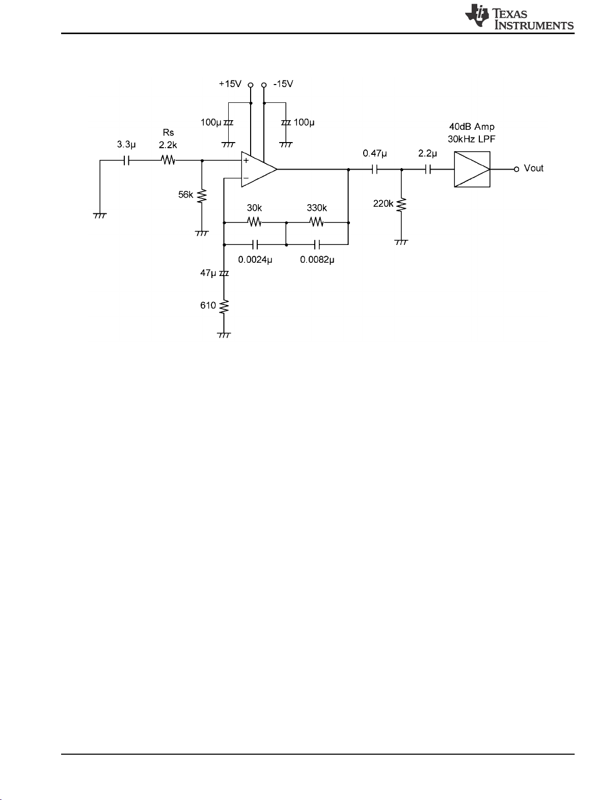
RIAA Noise Voltage Measurement Circuit
521855
10 Copyright © 1999-2012, Texas Instruments Incorporated
Page 11

LM833
RIAA Preamp Voltage Gain, RIAA
Deviation vs Frequency
Typical Applications
NAB Preamp
521828
Flat Amp Voltage Gain vs
Frequency
521829
NAB Preamp Voltage Gain
vs Frequency
AV = 34.5
F = 1 kHz
En = 0.38 μV
A Weighted
VO = V1–V2
521830
Balanced to Single Ended Converter
521832
521831
Adder/Subtracter
521833
VO = V1 + V2 − V3 − V4
Copyright © 1999-2012, Texas Instruments Incorporated 11
Page 12
LM833
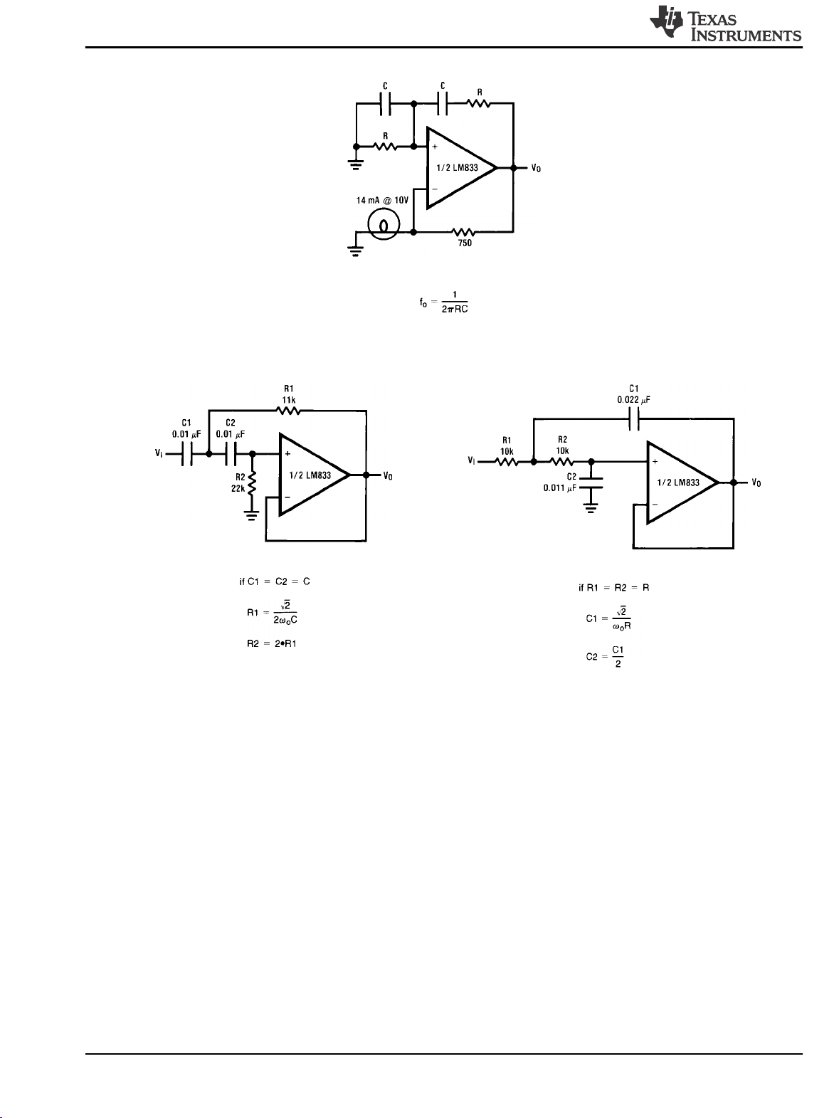
Sine Wave Oscillator
521834
Second Order High Pass Filter
Illustration is f0 = 1 kHz
(Butterworth)
521835
Second Order Low Pass Filter
(Butterworth)
521836
Illustration is f0 = 1 kHz
12 Copyright © 1999-2012, Texas Instruments Incorporated
Page 13
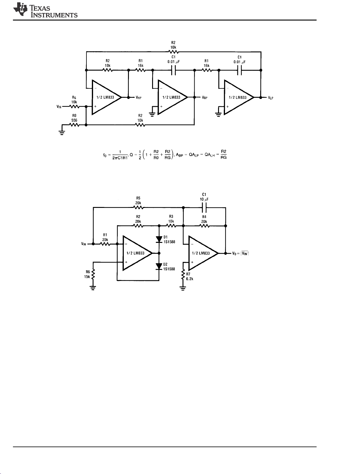
Illustration is f0 = 1 kHz, Q = 10, ABP = 1
LM833
State Variable Filter
521837
AC/DC Converter
521838
Copyright © 1999-2012, Texas Instruments Incorporated 13
Page 14

LM833
2 Channel Panning Circuit (Pan Pot)
521839
Line Driver
521840
Tone Control
Illustration is:
fL = 32 Hz, fLB = 320 Hz
fH =11 kHz, fHB = 1.1 kHz
521841
521842
14 Copyright © 1999-2012, Texas Instruments Incorporated
Page 15

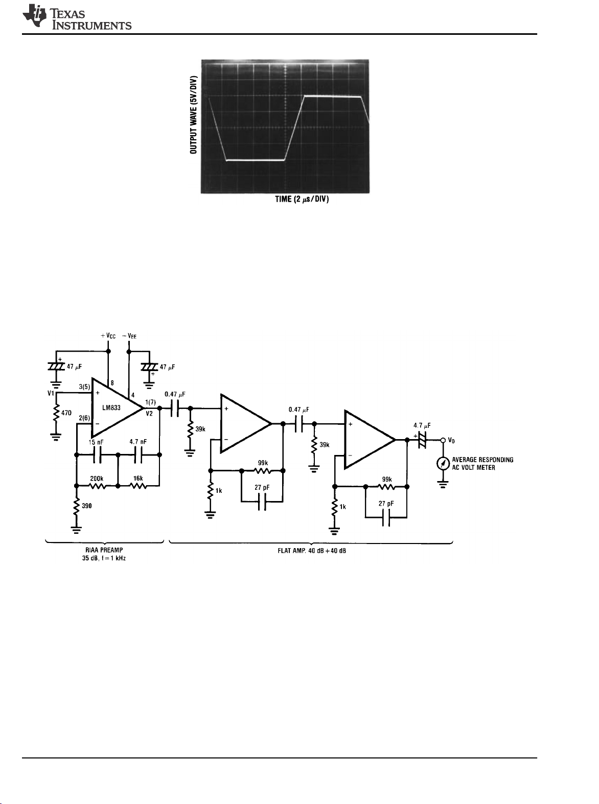
RIAA Preamp
LM833
Av = 35 dB
En = 0.33 μV
S/N = 90 dB
f = 1 kHz
A Weighted
A Weighted, VIN = 10 mV
@f = 1 kHz
521803
Balanced Input Mic Amp
521843
Illustration is:
V0 = 101(V2 − V1)
Copyright © 1999-2012, Texas Instruments Incorporated 15
Page 16

LM833
10 Band Graphic Equalizer
521844
fo (Hz) C
32
64
125
250
1
0.12μF 4.7μF 75kΩ 500Ω
0.056μF 3.3μF 68kΩ 510Ω
0.033μF 1.5μF 62kΩ 510Ω
0.015μF 0.82μF 68kΩ 470Ω
500 8200pF
1k 3900pF
2k 2000pF
4k 1100pF
8k 510pF
16k 330pF
Note 7: At volume of change = ±12 dB
Q = 1.7
Reference: “AUDIO/RADIO HANDBOOK”, National Semiconductor, 1980, Page 2–61
C
0.39μF 62kΩ 470Ω
0.22μF 68kΩ 470Ω
0.1μF 68kΩ 470Ω
0.056μF 62kΩ 470Ω
0.022μF 68kΩ 510Ω
0.012μF 51kΩ 510Ω
2
R
1
R
2
16 Copyright © 1999-2012, Texas Instruments Incorporated
Page 17

LM833 MDC MWC DUAL AUDIO OPERATIONAL AMPLIFIER
LM833
Die Layout (A - Step)
521854
Die/Wafer Characteristics
Fabrication Attributes General Die Information
Physical Die Identification LM833A Bond Pad Opening Size (min) 110µm x 110µm
Die Step A Bond Pad Metalization ALUMINUM
Physical Attributes Passivation VOM NITRIDE
Wafer Diameter 150mm Back Side Metal BARE BACK
Dise Size (Drawn)
Thickness 406µm Nominal
Min Pitch 288µm Nominal
Special Assembly Requirements:
Note: Actual die size is rounded to the nearest micron.
(Referenced to die center, coordinates in µm) NC = No Connection
SIGNAL NAME PAD NUMBER
OUTPUT A 1 -476 500 110 x 110
INPUT A- 2 -476 -212 110 x 110
INPUT A+ 3 -476 -500 110 x 110
VEE- 4 -0 -500 110 x 110
INPUT B+ 5 476 -500 110 x 110
INPUT B- 6 476 -212 110 x 110
OUTPUT B 7 476 500 110 x 110
VCC+ 8 0 500 110 x 110
1219µm x 1270µm
48mils x 50mils
Die Bond Pad Coordinate Locations (A - Step)
X/Y COORDINATES PAD SIZE
X Y X Y
Back Side Connection Floating
Copyright © 1999-2012, Texas Instruments Incorporated 17
Page 18

LM833
IN U.S.A
Tel #: 1 877 Dial Die 1 877 342 5343
Fax: 1 207 541 6140
IN EUROPE
Tel: 49 (0) 8141 351492 / 1495
Fax: 49 (0) 8141 351470
IN ASIA PACIFIC
Tel: (852) 27371701
IN JAPAN
Tel: 81 043 299 2308
18 Copyright © 1999-2012, Texas Instruments Incorporated
Page 19
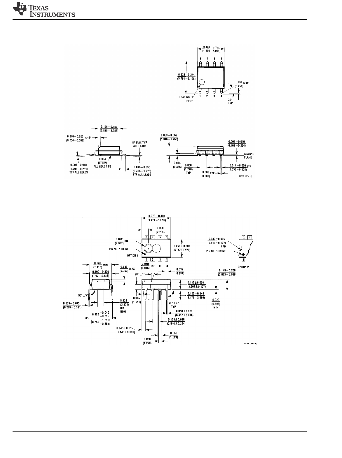
Physical Dimensions inches (millimeters) unless otherwise noted
LM833
Molded Small Outline Package (M)
Order Number LM833M or LM833MX
LM833AM, LM833AMX
NS Package Number M08A
Molded Dual-In-Line Package (N)
Order Number LM833N
NS Package Number N08E
Copyright © 1999-2012, Texas Instruments Incorporated 19
Page 20

LM833
8-Lead (0.118” Wide) Molded Mini Small Outline Package
Order Number LM833MM or LM833MMX
NS Package Number MUA08A
20 Copyright © 1999-2012, Texas Instruments Incorporated
Page 21

LM833
Copyright © 1999-2012, Texas Instruments Incorporated 21
Page 22

Notes
Copyright © 1999-2012, Texas Instruments
Incorporated
Page 23

IMPORTANT NOTICE
Texas Instruments Incorporated and its subsidiaries (TI) reserve the right to make corrections, enhancements, improvements and other
changes to its semiconductor products and services per JESD46C and to discontinue any product or service per JESD48B. Buyers should
obtain the latest relevant information before placing orders and should verify that such information is current and complete. All
semiconductor products (also referred to herein as “components”) are sold subject to TI’s terms and conditions of sale supplied at the time
of order acknowledgment.
TI warrants performance of its components to the specifications applicable at the time of sale, in accordance with the warranty in TI’s terms
and conditions of sale of semiconductor products. Testing and other quality control techniques are used to the extent TI deems necessary
to support this warranty. Except where mandated by applicable law, testing of all parameters of each component is not necessarily
performed.
TI assumes no liability for applications assistance or the design of Buyers’ products. Buyers are responsible for their products and
applications using TI components. To minimize the risks associated with Buyers’ products and applications, Buyers should provide
adequate design and operating safeguards.
TI does not warrant or represent that any license, either express or implied, is granted under any patent right, copyright, mask work right, or
other intellectual property right relating to any combination, machine, or process in which TI components or services are used. Information
published by TI regarding third-party products or services does not constitute a license to use such products or services or a warranty or
endorsement thereof. Use of such information may require a license from a third party under the patents or other intellectual property of the
third party, or a license from TI under the patents or other intellectual property of TI.
Reproduction of significant portions of TI information in TI data books or data sheets is permissible only if reproduction is without alteration
and is accompanied by all associated warranties, conditions, limitations, and notices. TI is not responsible or liable for such altered
documentation. Information of third parties may be subject to additional restrictions.
Resale of TI components or services with statements different from or beyond the parameters stated by TI for that component or service
voids all express and any implied warranties for the associated TI component or service and is an unfair and deceptive business practice.
TI is not responsible or liable for any such statements.
Buyer acknowledges and agrees that it is solely responsible for compliance with all legal, regulatory and safety-related requirements
concerning its products, and any use of TI components in its applications, notwithstanding any applications-related information or support
that may be provided by TI. Buyer represents and agrees that it has all the necessary expertise to create and implement safeguards which
anticipate dangerous consequences of failures, monitor failures and their consequences, lessen the likelihood of failures that might cause
harm and take appropriate remedial actions. Buyer will fully indemnify TI and its representatives against any damages arising out of the use
of any TI components in safety-critical applications.
In some cases, TI components may be promoted specifically to facilitate safety-related applications. With such components, TI’s goal is to
help enable customers to design and create their own end-product solutions that meet applicable functional safety standards and
requirements. Nonetheless, such components are subject to these terms.
No TI components are authorized for use in FDA Class III (or similar life-critical medical equipment) unless authorized officers of the parties
have executed a special agreement specifically governing such use.
Only those TI components which TI has specifically designated as military grade or “enhanced plastic” are designed and intended for use in
military/aerospace applications or environments. Buyer acknowledges and agrees that any military or aerospace use of TI components
which have not been so designated is solely at the Buyer's risk, and that Buyer is solely responsible for compliance with all legal and
regulatory requirements in connection with such use.
TI has specifically designated certain components which meet ISO/TS16949 requirements, mainly for automotive use. Components which
have not been so designated are neither designed nor intended for automotive use; and TI will not be responsible for any failure of such
components to meet such requirements.
Products Applications
Audio www.ti.com/audio Automotive and Transportation www.ti.com/automotive
Amplifiers amplifier.ti.com Communications and Telecom www.ti.com/communications
Data Converters dataconverter.ti.com Computers and Peripherals www.ti.com/computers
DLP® Products www.dlp.com Consumer Electronics www.ti.com/consumer-apps
DSP dsp.ti.com Energy and Lighting www.ti.com/energy
Clocks and Timers www.ti.com/clocks Industrial www.ti.com/industrial
Interface interface.ti.com Medical www.ti.com/medical
Logic logic.ti.com Security www.ti.com/security
Power Mgmt power.ti.com Space, Avionics and Defense www.ti.com/space-avionics-defense
Microcontrollers microcontroller.ti.com Video and Imaging www.ti.com/video
RFID www.ti-rfid.com
OMAP Mobile Processors www.ti.com/omap TI E2E Community e2e.ti.com
Wireless Connectivity www.ti.com/wirelessconnectivity
Mailing Address: Texas Instruments, Post Office Box 655303, Dallas, Texas 75265
Copyright © 2012, Texas Instruments Incorporated
Page 24

Mouser Electronics
Authorized Distributor
Click to View Pricing, Inventory, Delivery & Lifecycle Information:
Texas Instruments:
LM833M LM833M/NOPB LM833MM LM833MM/NOPB LM833MMX LM833MMX/NOPB LM833MX
LM833MX/NOPB LM833N LM833N/NOPB
 Loading...