

Page 1

User's Guide
SNVU543A–November 2016–Revised December 2016
LM5170-Q1 EVM User Guide
The LM5170EVM-BIDIR Evaluation Module (EVM) is designed to showcase the LM5170-Q1 high
performance dual-channel bidirectional controller suitable for, but not limited to, the automotive 48-V to 12V dual battery system applications.
The EVM can be configured to achieve a bidirectional power converter in the form of either the current
source or voltage source. The direction of power flow can be controlled either by an external command
signal or by the on-board jumper. Through the onboard interface headers, the EVM can be operated by a
DSP, an FPGA, an MCU, or other digital controllers. Two EVMs can be paralleled to make a 3 or 4
phases interleaved converter for higher power. More EVMs can be paralleled for greater number of
phases. Many convenient jumper headers are also included for versatile configurations of the EVM.
Refer to the LM5170-Q1 Multiphase Bidirectional Current Controller Datasheet (SNVSAQ6) for detailed
technical information of the LM5170-Q1 device.
Contents
1 Features and Electrical Performance ..................................................................................... 3
2 Setup .......................................................................................................................... 4
3 Test Procedure ............................................................................................................. 12
4 Test Data .................................................................................................................... 14
5 Design Files................................................................................................................. 19
List of Figures
1 Simplified EVM Schematic ................................................................................................. 5
2 EVM Board Top View and Layout Partitions............................................................................. 6
3 Bidirectional Converter Bench Setup .................................................................................... 11
4 Buck Mode Efficiency vs Input Voltage and Load Current: V
5 Boost Mode Efficiency vs Input Voltage and Load Current: V
6 Channel DC Current Regulation vs ISETA: Buck Mode .............................................................. 14
7 Channel DC Current Regulation vs ISETA: Boost Mode ............................................................. 14
8 ISETD to ISETA Conversion.............................................................................................. 14
9 Current Sharing Between Two Channels ............................................................................... 14
10 EVM Enable Power-Up Sequence....................................................................................... 15
11 EVM Shutdown by nFAULT............................................................................................... 15
12 Buck Mode Enable......................................................................................................... 15
13 Boost Mode Enable........................................................................................................ 15
14 Dual-Channel Interleaving Operation in Buck Mode: 20 A Per Channel ........................................... 15
15 Dual-Channel Interleaving Operation in Boost Mode: 20 A Per Channel........................................... 15
16 Inductor Current Tracking: Buck Mode.................................................................................. 16
17 Inductor Current Tracking: Boost Mode ................................................................................. 16
18 Diode Emulation During Start-Up ........................................................................................ 16
19 Diode Emulation During Shutdown ...................................................................................... 16
20 Diode Emulation in DCM.................................................................................................. 16
21 Response to Dynamic DIR Change ..................................................................................... 17
22 Step Load Response: Buck Mode; 20-A to 50-A Load Step 1A/μs.................................................. 17
23 Step Load Response: Boost Mode, 5-A to 10-A Load Step 1A/μs .................................................. 17
= 14.5 V.......................................... 14
OUT
= 50.5 V......................................... 14
OUT
SNVU543A–November 2016–Revised December 2016
Submit Documentation Feedback
Copyright © 2016, Texas Instruments Incorporated
LM5170-Q1 EVM User Guide
1
Page 2

www.ti.com
24 OVP in Buck Mode......................................................................................................... 17
25 OVP in Boost Mode........................................................................................................ 17
26 Output Short Circuit: Buck Mode......................................................................................... 18
27 EVM Schematic Part 1: Power Circuit................................................................................... 19
28 EVM Schematic Part 2: Control Circuit.................................................................................. 20
29 EVM Schematic Part 3: Bias Supplies .................................................................................. 21
30 EVM Schematic Part 4: Optional Outer Voltage Loop Control Circuit .............................................. 22
31 EVM Schematic Part 5: Interface Connectors and Configuration Headers......................................... 23
32 EVM Top Layer Silkscreen................................................................................................ 27
33 EVM Top Layer Copper ................................................................................................... 28
34 EVM Middle Layer 1 ....................................................................................................... 29
35 EVM Middle Layer 2 ....................................................................................................... 30
36 EVM Middle Layer 3 ....................................................................................................... 31
37 EVM Middle Layer 4 ....................................................................................................... 32
38 EVM Middle Layer 5 ....................................................................................................... 33
39 EVM Middle Layer 6 ....................................................................................................... 34
40 EVM Bottom Layer Copper ............................................................................................... 35
41 EVM Bottom Layer Silkscreen............................................................................................ 36
List of Tables
1 Electrical Performance...................................................................................................... 4
2 Three-Pin Header Settings................................................................................................. 7
3 Two-Pin Header Settings................................................................................................... 8
4 J17 60-Pin Header Description ............................................................................................ 9
5 J18 60-Pin Header Description........................................................................................... 10
6 Bill of Materials ............................................................................................................. 24
Trademarks
2
LM5170-Q1 EVM User Guide
Copyright © 2016, Texas Instruments Incorporated
SNVU543A–November 2016–Revised December 2016
Submit Documentation Feedback
Page 3

www.ti.com
1 Features and Electrical Performance
The EVM supports the following features and performance capabilities:
• Input Operating Voltage Ranges
– The 48VDC-Port 6 V to 75 V, in the Buck Mode
– The 12VDC-Port 3 V to 48 V, in the Boost Mode
• Output Voltage Regulation (With the Onboard Outer Voltage Loop Control Activated)
– 14.5-V Output Voltage at the 12VDC-Port, in the Buck Mode
– 50.5-V Output Voltage at the 48VDC-Port, in the Boost Mode
• Operating Current
– 60-Adc Maximum from or into the 12VDC-Port
– Typical 1% Current Regulation Accuracy
– Typical 1% Current Monitor Accuracy
• Switching Frequency:
– Standalone Fsw = 100 kHz
– Able to Synchronize to an External Clock from 80 kHz to 120 kHz.
• Maximum Efficiency: >97%
• OVP Threshold
– 75 V at the 48VDC-Port
– 22 V at the 12VDC-Port
– Synchronous Rectifier Diode Emulation Function Preventing Negative Current
• Other Convenient Features
– Optional Onboard Wide-VIN™ LM5118-Q1 Buck-Boost Converter as the +10-V Supply
– Onboard Ultra Low IQ TPS709-Q1 LDOs for +3.3-V and +5.0-V Bias Voltages for Convenient EVM
Configurations and for Biasing the External MCU through Headers.
– Onboard LM26LV Temperature Sensors Monitoring Local Temperatures of Power MOSFETs, With
Optional Overtemperature Shutdown and LED Indicator.
– LED indicators of Buck and Boost Operating Modes.
– Optional Channel Current Shunt AC Filters for Accurate DVM Reading (Unpopulated).
The electrical performance of the EVM is show in Table 1. Figure 1 shows the simplified EVM schematic.
Features and Electrical Performance
SNVU543A–November 2016–Revised December 2016
Submit Documentation Feedback
Copyright © 2016, Texas Instruments Incorporated
LM5170-Q1 EVM User Guide
3
Page 4

Setup
www.ti.com
Table 1. Electrical Performance
PARAMETER TEST CONDITIONS MIN TYP MAX UNIT
INPUT CHARACTERISTICS
48VDC-Port Buck mode operation (DIR > 2 V) 6 48 70 V
12VDC-Port Boost mode operation (DIR < 1 V) 3 12 48 V
OUTPUT CHARACTERISTICS
Current delivery
Current regulation accuracy 12VDC-Port current vs ISETA command voltage 1%
Channel current monitor
accuracy
48VDC-Port
12VDC-Port
SYSTEM CHARACTERISTICS
Switching frequency 100 kHz
External clock
synchronization
Full load efficiency 97%
Junction temperature, T
12VDC-Port input or output current (dual-channel
enabled)
When onboard IOUT1 and IOUT2 termination filter
activated
Boost mode operation (DIR < 1 V, onboard analog
output voltage loop closed)
Buck mode operation (DIR > 2 V, onboard analog
output voltage loop closed)
J
0 60 A
1%
50.5 V
14.5 V
80 120 kHz
–40 150 °C
2 Setup
2.1 EVM Configurations
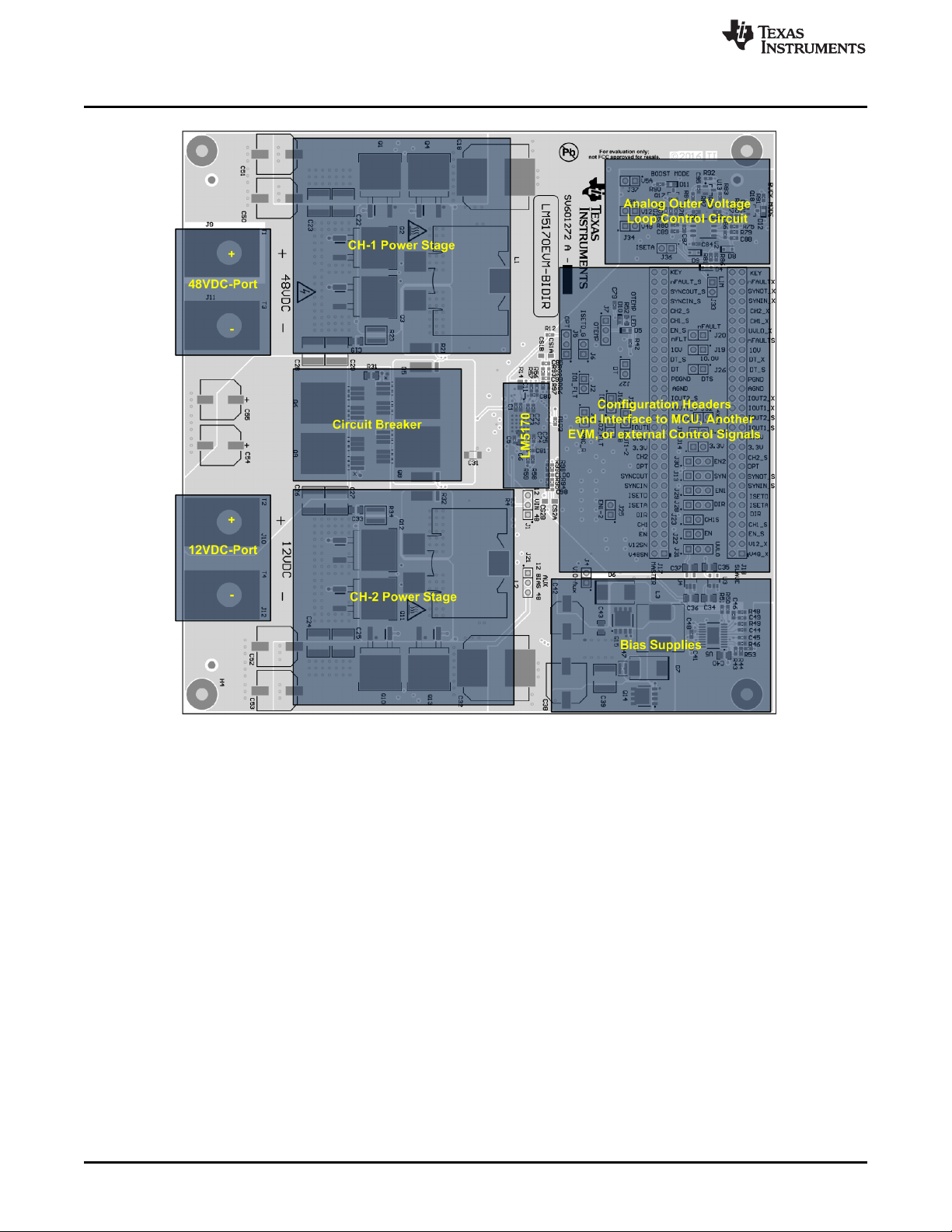
Figure 2 shows the EVM board top view and circuit layout partitions. The EVM has the following ports:
• 48VDC-Port: Connected to 48-V battery rail
• 12VDC-Port: Connected to 12-V battery rail
• J17 (60-Pin Header): Interfacing the external control commands or MCU
• J18 (60-Pin Header): Interfacing the slave EVM’s J17 in a 4-phase system consisting of two EVMs
• Master Enable Using J17-pin 5: Providing a voltage of 2.5 V to 6 V to operate the EVM.
• Channel Current Setting: Analog programming at J17-pin 11, and digital programming at J17-pin 13.
Table 2 through Table 5 list the functions of the EVM jumpers and headers. They offer flexible
configurability and programmability of the EVM for various use cases including but not limited to the
following:
• A unidirectional or bidirectional current source
• A unidirectional or bidirectional voltage source
• Dynamic phase adding and shedding in a 4-phase system consisting of two EVMs
• Dynamic MOSFETs dead time adjustment
• Individual channel current monitoring or total current monitoring
• Programmable undervoltage lockout (unpopulated)
• Synchronization to external clock
• External shutdown command through nFAULT pin (J17-pin45)
4
LM5170-Q1 EVM User Guide
Copyright © 2016, Texas Instruments Incorporated
SNVU543A–November 2016–Revised December 2016
Submit Documentation Feedback
Page 5

+
12VDC-Port
-
23
4.7 µH
1 m
20
22 36 35
470 µF
PGND
6
19
2.2 µF
PGND
34
33
VIN
HO1
HB1
LO1
CSA1
CSB1
BRKG
BRKSVCC
31 VCCA
24.9
1 µF
46 AGND
44
10
39
DIR
UVLO
EN1
43
EN2
40
AGND
42 ISETD
45
ISETA
SYNCIN
41
SYNCOUT
4
28
8
95.3 k
1 nF
VINX
RAMP1
RAMP2
14
0.22 µF
PGND
4.7 µH
1 m
17
15
1 2
PGND
HO2
HB2
LO2
CSA2
CSB2
9.09 k
ENABLE
DIR
ISETA
+
+10Vdc
-
1 nF
26COMP1
11COMP2
15 nF
634
VCC
VCC
1 nF
15 nF
634
1 nF
12
25
9
AGND
SS
OVPA
OVPB
48DT
10 nF
10 k
51.1 k
54.9 k
30IPK
40.2 k
29 OPT
37
IOUT1
38
IOUT2
9.09 k
10 k
47 OSC
40.2 k
10 nF
10 nF
AGND
24
SW1
13
SW2
0.22 µF
IOUT1
IOUT2
27
nFAULT
PGND
+
48VDC-Port
-
VCC
100 µF
100 µF
PGND
470 µF
LM5170-Q1
CMMD AND
MONITOR
C2
C1
C
HB1
Q
H1
Q
L2
C
VCC
C5
C
IOUT1
C
IOUT2
C8
C
HB2
C10
C
SS
C
HF1
C
COMP1
C
RAMP2
C
RAMP1
Q
H2
Q
L2
R
CS2
R
VCCA
R
OSC
R
SYNCO
R
IOUT1
R
IOUT2
R
IPK
R
OVPB
R
OVPA
R
DT
R
COMP1
R
RAMP2
R
RAMP1
R
BRK
D
HB1
D
HB2
18
PGND
PGND
PGND
AGND
C
COMP2
R
COMP2
C
HF2
1 M
L
m1
R
CS1
L
m2
PGND
95.3 k
95.3 NŸ
www.ti.com
Setup
SNVU543A–November 2016–Revised December 2016
Submit Documentation Feedback
Figure 1. Simplified EVM Schematic
Copyright © 2016, Texas Instruments Incorporated
LM5170-Q1 EVM User Guide
5
Page 6
Setup
www.ti.com
6
LM5170-Q1 EVM User Guide
Figure 2. EVM Board Top View and Layout Partitions
SNVU543A–November 2016–Revised December 2016
Submit Documentation Feedback
Copyright © 2016, Texas Instruments Incorporated
Page 7
www.ti.com
Table 2. Three-Pin Header Settings
HEADER SIGNAL PINS FUNCTION DESCRIPTION DEFAULT
(1)
J1 —
J5 OPT
J7 OTEMP
J13 SYNC
J21 BIAS
J28 DIR
J29 EN1
J30 EN2
J31 UVLO
(1)
– = All jumper pins open.
(2)
(1,2) = Pins 1 and 2 closed.
(3)
(2,3) = Pins 2 and 3 closed.
--
(2)
(1,2)
(3)
(2,3)
-- External interleaving control through J17
(1,2) CH-2 240 degree delay from CH-1
(2,3) CH-2 180 degree delay from CH-1 Y
-- Onboard Overtemperature protection disabled Y
(1,2) Overtemperature protection in hiccup mode
(2,3) Overtemperature protection in latched shutdown
-- Slave EVM not sync to master EVM Y
(1,2) Slave EVM sync to master via J18
(2,3) Slave EVM sync to external Clock
-- Use external 10V supply
(1,2) Onboard +10V produced from the 12VDC-Port
(2,3) Onboard +10V produced from the 48VDC-Port Y
-- External DIR control through J17
(1,2) Onboard DIR command for buck operation Y
(2,3) Onboard DIR command for boost operation
-- External CH-1 enable control through J17
(1,2) Onboard CH-1 enable Y
(2,3) Onboard CH-1 disable
-(1,2) Onboard CH-2 enable
(2,3) Onboard CH-2 disable
-- External EVM enable through J17 Y
(1,2)
(2,3) EVM disable
No UVLO Programming Y
48VDC-Port UVLO Control
12VDC-Port UVLO Control
External CH-1 enable control through J17, overridden by
J25.
Onboard EVM enable, if external 3.3V is supplied to J17pin23.
Setup
Y
SNVU543A–November 2016–Revised December 2016
Submit Documentation Feedback
Copyright © 2016, Texas Instruments Incorporated
LM5170-Q1 EVM User Guide
7
Page 8

Setup
Table 3. Two-Pin Header Settings
HEADER SIGNAL PINS FUNCTION DESCRIPTION DEFAULT
J2 IOUT1
J3 SYNCOUT
J4 VCC
J6 ISETD
J8 IOUT2
J14 3.3 V
J15 5 V
J16 IOUT_All
J19 10 V
J20 nFAULT
J22 EN
J23 CH1S
J24 IOUT1-2
J25 EN1-2
J26 DTS
J27 DT
J32 OPT/ EN2_slave
J33 ILIM
J34 48VDC Sense
J35 12VDC Sense
J36 ISETA
J37 5 V
(1)
Jumper pins open.
(2)
Jumper pins closed.
(1)
O
(2)
C
O Enable the fault detection Y
C Disable the fault detection disabled
O An external 10-V supply as VCC supply Y
C The onboard 10-V regulator as VCC supply
O ISETD input disabled
C ISETD input is enabled Y
O External IOUT2 signal termination
C Onboard IOUT2 signal termination Y
O Onboard 3.3-V bias voltage disconnected from the slave EVM Y
C Onboard 3.3-V bias voltage feeding the slave EVM
O Onboard 5-V bias voltage disconnected from the slave EVM Y
C Onboard 5-V bias voltage feeding the slave EVM
O Independent channel monitor Y
C
O 10-V bias voltage disconnected from the slave EVM Y
C 10-V bias voltage feeding the slave EVM
O Independent master/slave nFAULT signal Y
C Combined master/slave nFAULT signal
O Independent enable control of the master and slave EVMs Y
C Combined enable control of the master and slave EVMs
O Independent slave EVM CH-1 enable Y
C Combined master/slave channel enable
O Independent channel current monitors Y
C Combined dual-channel current monitor
O Independent channel enable Y
C Combined dual-channel enable
O Independent DT adjustment input for the slave EVM Y
C Combined DT adjustment for both the master and slave EVMs
O External programmable DT adjustment input Y
C Onboard DT setting
O 3- and 4-phase transition disabled Y
C 3- and 4-phases transition enabled
O External current limit control input Y
— Do not close
O Boost analog outer voltage loop control disabled Y
C Boost analog outer voltage loop control enabled
O Buck analog outer voltage loop control disabled Y
C Buck analog outer voltage loop control enabled
O Analog outer voltage loop control disabled Y
C Analog outer voltage loop control enabled
O Analog outer voltage loop control disabled Y
C Analog outer voltage loop control enabled
External IOUT1 termination
Onboard IOUT1 termination Y
Combined total monitor in master/slave configuration. Requiring
J25 to be closed too.
www.ti.com
8
LM5170-Q1 EVM User Guide
SNVU543A–November 2016–Revised December 2016
Submit Documentation Feedback
Copyright © 2016, Texas Instruments Incorporated
Page 9

www.ti.com
Table 4. J17 60-Pin Header Description
(1)
PIN SIGNAL I/O DESCRIPTION
1 V48SN O
(2)
48V-port voltage sense during operation
3 V12SN O 12V-port voltage sense during operation
5
EN (MASTER
ENABLE)
(3)
I
Master EVM enable (connect to the UVLO pin of the IC)
7 CH1 I CH-1 control (connect to the EN1 pin of the IC)
9 DIR I Direction command
11 ISETA I Channel current setting (analog voltage)
13 ISETD I Channel current setting (PWM signal)
15 SYNCIN I Input of the external clock to be synchronized to
17 SYNCOUT O Clock output signal
19 OPT I Interleave angle setting
21 CH2 I CH-2 control (connect to the EN2 pin of the IC)
23 +3.3 V O Output of onboard +3.3-V voltage
25 +5 V O Output of onboard +5-V voltage
27 IOUT1 O CH-1 monitor
29 IOUT2 O CH-2 current monitor
31 IOUT1_S O Slave EVM CH-1 monitor in 3 or 4 phases
33 IOUT2_S O Slave EVM CH-2 current monitor in 3 or 4 phases
35 AGND I/O Reference GND for control signals
37 PGND O Power ground of the DC-DC converter
39 DT I Dead time adjustment pin
41 DT_S I Slave dead time adjustment pin
43 +10 V I/O Input of +10-V bias supply, or output of onboard +10-V bias supply
45 nFAULT I/O Fault report flag, or external shutdown command pin
47 ENABLE_S I Slave EVM enable (connect to the UVLO pin of the slave IC)
49 CH1_S I Slave EVM CH-1 control (connect to the EN1 pin of the slave IC)
51 CH2_S I Slave EVM CH-2 control (connect to the EN2 pin of the slave IC)
53 SYNCIN_S I Input of the external clock for the slave to be synchronized to
55 SYNCOUT_S O Slave EVM clock output signal
57 nFAULT_S I/O Slave EVM fault report flag, or external shut down command input pin
59 KEY — No Connect
All even
number pins
(1)
J17 is the interface connector to MCU, or external digital controller, or to the master EVM’s J18 if the host EVM serves as a slave in the
multiphase configuration.
(2)
I = input pin
(3)
O = output pin
AGND I/O All signals’ return
Setup
SNVU543A–November 2016–Revised December 2016
Submit Documentation Feedback
Copyright © 2016, Texas Instruments Incorporated
LM5170-Q1 EVM User Guide
9
Page 10

Setup
Table 5. J18 60-Pin Header Description
PIN SIGNAL I/O DESCRIPTION
1 V48_X — No Connect
3 V12_X — No Connect
5 ENABLE_S I
7 CH1_S I Slave EVM CH-1 control (connect to the EN1 pin of the IC)
9 DIR I Direction command
11 ISETA I Channel current setting (analog voltage)
13 ISETD I Channel current setting (PWM signal)
15 SYNCIN_S I The external clock input for the slave
17 SYNCOUT_S O
19 OPT I Interleave angle setting
21 CH2_S I Slave EVM CH-2 control (connect to the EN1 pin of the IC)
23 +3.3 V I Output of onboard +3.3-V voltage
25 +5 V I Output of onboard +5-V voltage
27 IOUT1_S O Slave EVM CH-1 monitor in 3 or 4 phases
29 IOUT2_S O Slave EVM CH-2 current monitor in 3 or 4 phases
31 IOUT1_X — Not used
33 IOUT2_X — Not used
35 AGND I/O Reference GND for control signals
37 PGND O Power ground of the DC-DC converter
39 DT_S I Slave EVM dead time adjustment pin
41 DT_X — No Connect
43 +10 V I Input of +10-V bias supply, or output of onboard +10-V bias supply
45 nFAULT_X I/O Slave EVM fault report flag, or external shutdown command pin
47 UVLO_X — No Connect
49 CH1_X — No Connect
51 CH2_X — No Connect
53 SYNCIN_X — No Connect
55 SYNCOUT_X — No Connect
57 nFAULT_X — No Connect
59 KEY — No Connect
All even
number pins
(1)
J18 is the interface connector to the slave EVM in the multiphase configuration if the host EVM serves as the master. All control
commands and control signals are sent through J18 to the slave EVM’s J17.
(2)
I = input pin
(3)
O = output pin
AGND I/O All signals’ return
(2)
(3)
Slave EVM enable (connect to the UVLO pin of the slave IC)
Slave EVM clock output signal
(1)
www.ti.com
10
LM5170-Q1 EVM User Guide
SNVU543A–November 2016–Revised December 2016
Copyright © 2016, Texas Instruments Incorporated
Submit Documentation Feedback
Page 11
LM5170-Q1 EVM
+
-
+10 V UVLO EN1/2 DIR
ISETA or
ISETD
+
-
48 VDC
12 VDC
RTN
RTN
HV-PS
LV-PSHV-E-Load
LV-E-Load
www.ti.com
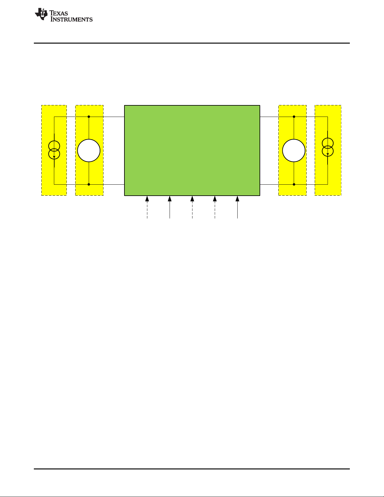
2.2 Bench Setup
Figure 3 shows the typical bench setup to operate the EVM in the bidirectional power system environment.
The combination of the Electronic Load (E-Load) and bench Power Supply (PS) emulates a battery
capable of both sourcing and sinking current. A relatively Higher Voltage Power Supply (HV-PS) and ELoad (HV-E-Load) should be used for the 48VDC-port, and a Lower Voltage Power Supply (LV-PS) and
E-Load (LV-E-Load) for the 12VDC-port. The external control signals shown as dashed lines can also be
created with the onboard headers.
Setup
To operate the EVM to full power, the initial setup should follow the guidelines below:
• Set the LV-E-Load to Constant Current (CC) of 62 A
• Set the LV-PS voltage at 12 V, and the current limit at 63 A
• Set the HV-E-Load to CC of 14 A
• Set the HV-PS voltage at 48 V, and the current limit at 15 A
Note that in Buck Mode operation, the HV-E-load can be turned off, and in Boost Mode operation, the LV-
E-load can be turned off. If the output voltage loop is closed, the LV-PS can be disconnected in Buck
Mode operation. In Boost Mode operation, the HV-PS is required for Boost start-up, which is limited by the
onboard circuit breaker function. If the circuit breaker MOSFETS are shorted and J3 is closed, the HV-PS
is not needed for Boost Mode operation.
2.3 Test Equipment
Power Supplies: HV-PS should be capable of 80V/20A, and LV-PS 40V/80A. To operate 2 EVMs in 4
phase configuration, the HV-PS and LV-PS capabilities should be doubled. Bench power supplies to
generate UVLO, ISETA, DIR, and EN1 and EN2 signals should be capable of 5V/0.1A.
Electronic Loads: The HV-E-Load should be capable of 80V/20A, and LV-E-Load 40V/80A. To operate 2
EVMs in 4 phase configuration, the E-Loads’ capabilities should be doubled.
Meters: Because most current meters are rated only to 10 A, shunts are recommended to measure the
current using a DVM.
Oscilloscope: An oscilloscope and 10x probes with at least 20-MHz bandwidth is required. Current probe
capable of 50 A is required to monitor the inductor current via a wire loop inserted to the non-switching
side of the inductor.
Figure 3. Bidirectional Converter Bench Setup
SNVU543A–November 2016–Revised December 2016
Submit Documentation Feedback
Copyright © 2016, Texas Instruments Incorporated
LM5170-Q1 EVM User Guide
11
Page 12

Test Procedure
3 Test Procedure
Please read the LM5170-Q1 datasheet (SNVSAQ6) and this user guide before using the EVM. A typical
EVM test bench setup is shown in Figure 2. The power supplies and loads should be capable of handling
the input and output voltage and current rating of the board.
The EVM operation requires the four external control signals, which are UVLO, DIR, EN1/2, and ISETA or
ISETD (refer to Figure 3).
• UVLO: The master enable command. Apply a voltage > 2.5 V and < 6 V between J17-pins 5 and 6 to
enable the EVM. Pulling the voltage at J17-pin 5 low will keep the EVM in shutdown mode.
• DIR: the current direction command. Apply a voltage > 2 V at J17-pin 9 or J18-pin 9 to operate the
EVM in Buck Mode. Apply a voltage < 1 V at the same pin to operate the EVM in Boost Mode. DIR
command can also be programmed using J28. Note that DIR must be either active high or low to
operate the EVM. If the DIR signal is floating, the EVM will not run.
• EN1 and EN2: The channel switching enable commands. Apply a voltage > 2 V at J17-pin 7 will turn
on CH-1 converter, and at J17-pin 21 will turn on CH-2 converter. Removing the voltage at the EN1
and EN2 pins to disable each channel. The channel enable can also be controlled by J29, J30 and
J25.
• ISETA or ISETD: The Channel current regulation setting. Applying an analog voltage across J17-pins
11 and 12, or J18-pins 11 and 12, or a PWM signal across J17-pins 13 and 14, or J18-pins 13 and 14,
the EVM will regulate the channel DC current, which is also the power inductor dc current, to a level
proportional the ISETA voltage or ISETD PWM duty ratio. ISETA is controlled by the onboard analog
outer voltage control loop when it is closed. Note that, ISETA=1.5 V, or ISETD PWM duty ratio of 48%,
will command the EVM to produce 60 A into or out of the 12VDC-port, depending on the operation
mode.
For initial test, TI recommends using the onboard 10-V bias supply by closing the J4 and J21-pins 2 and
3. The user can also apply an external 10-V bias supply between J17-Pins 43 and 44, but remember to
open J4 and J21 in order to disable the onboard 10-V bias supply.
www.ti.com
3.1 Buck Mode Power-Up and Power-Down Sequence
1. Refer to Table 2 through Table 5 for proper jumper settings
2. Turn on the HV-PS power supply.
3. Turn on the LV-PS power supply and LV-E-Load.
4. Apply a voltage > 2.5 V and < 6 V at J17-pin 5 (Master Enable).
5. Apply an analog voltage gradually rising from 0V to 1.5V at J17-pin 11 or J18-pin 11 (ISETA), or a
PWM signal of duty ratio of 0 to 48% at J17-pin 13 or J18-pin 13.
6. Perform the test.
7. After the tests are done, turn off the ISETA or ISETD signal, remove the voltage at J17-pin 5, and turn
off the E-Load, LV-PS and HV-PS.
12
LM5170-Q1 EVM User Guide
SNVU543A–November 2016–Revised December 2016
Copyright © 2016, Texas Instruments Incorporated
Submit Documentation Feedback
Page 13

www.ti.com
3.2 Boost Mode Power-Up and Power-Down Sequence
1. Refer to Table 2 through Table 5 for proper jumper settings.
2. Turn on the HV-PS power supply and HV-E-Load.
3. Turn on the LV-PS power supply.
4. Apply a voltage > 2.5 V and < 6 V at J17-pin 5 (Master Enable).
5. Apply an analog voltage gradually rising from 0 V to 1.5 V at J17-pin 11 or J18-pin 11 (ISETA), or a
PWM signal of duty ratio of 0 to 48% at J17-pin 13 or J18-pin 13.
6. Perform the test.
7. After the tests are done, turn off the ISETA or ISETD signal, remove the voltage at J17-pin 5, and turn
off the E-Load, HV-PS and LV-PS.
3.3 Bidirectional Operation Power-Up and Power-Down Sequence
1. Refer to Table 2 through Table 5 for proper jumper settings.
2. Turn on the HV-PS power supply and HV-E-Load.
3. Turn on the HV-PS power supply and HV-E-Load.
4. Apply a voltage > 2.5 V and < 6 V at J17-pin 5 (Master Enable).
5. Apply the direction command (DIR) at J17-pin 9 or J18-pin 9.
6. Apply an analog voltage gradually rising from 0 V to 1.5 V at J17-pin 11 or J18-pin 11 (ISETA), or a
PWM signal of duty ratio of 0 to 48% at J17-pin 13 or J18-pin 13.
7. Dynamically flip the DIR signal state between 0 (DIR < 1 V) and 1 (DIR > 2 V), the EVM will operate in
dynamic bidirectional transition mode.
8. Perform the test.
9. After the tests are done, turn off the ISETA or ISETD signal, turn off the DIR signal, remove the voltage
at J17-pin 5, and turn off the E-Load, HV-PS and LV-PS.
Test Procedure
3.4 Operating the EVM With the Onboard Analog Loop Control Circuit
1. J34 through J37 headers must be closed to activate the onboard analog voltage loop control circuit.
2. To operate the EVM as a regulated voltage source, follow the power up and power down sequence for
buck mode or boost mode operation whichever is appropriate.
3. Note that with the circuit breaker MOSFETs employed by the EVM, HVPS should be applied for boost
start-up. After the start-up, it can be turned off. Only after the circuit breaker MOSFETs are replaced
with a direct short across the breaker will the EVM not require the HV-PS to assist boost start-up.
3.5 Operating the EVM With External MCU or Other Digital Circuit
1. Onboard analog voltage loop control circuit must be disconnected.
2. Use J17 header to interface the external MCU or other control circuit.
3. Follow the power-up and power-down sequence for buck mode or boost mode operation.
Signals required from an MCU or other digital control circuit include UVLO, EN1/EN2, DIR, ISETA or
ISETD. Contact TI for info on operating the EVM with the MSP431 Launchpad or C2000 MCU.
SNVU543A–November 2016–Revised December 2016
Submit Documentation Feedback
Copyright © 2016, Texas Instruments Incorporated
LM5170-Q1 EVM User Guide
13
Page 14

Duty Ratio of ISETD PWM Signal
ISETA Voltage (V)
0 20% 40% 60% 80% 100%
0
0.5
1
1.5
2
2.5
3
3.5
ISETA (V)
V_Ideal (V)
ISETA Voltage (V)
Channel DC Current (A)
0 200 400 600 800 1000 1200
0
5
10
15
20
25
CH1 Current
CH2 Current
ISETA Voltage (mV)
Regulation Error (A)
0 200 400 600 800 1000 1200 1400 1600 1800
-1
-0.8
-0.6
-0.4
-0.2
0
0.2
Regulation Error (A)
Ideal Current (A)
-5
0
5
10
15
20
25
30
35
Channel DC Current (A)
ISETA Voltage (mV)
Regulation Error (A)
0 200 400 600 800 1000 1200 1400 1600 1800
-0.45
-0.4
-0.35
-0.3
-0.25
-0.2
-0.15
-0.1
-0.05
0
0.05
Regulation Error (A)
Ideal Current (A)
0
5
10
15
20
25
30
35
Channel DC Current (A)
Load Current (A)
Efficiency (%)
0 10 20 30 40 50 60
80
82
84
86
88
90
92
94
96
98
100
D001
VIN = 24 V
VIN = 36 V
VIN = 48 V
VIN = 60 V
Load Current (A)
Efficiency (%)
0 2 4 6 8 10 12 14
80
82
84
86
88
90
92
94
96
98
100
VIN = 16 V
VIN = 12 V
VIN = 8 V
Test Data
4 Test Data
4.1 Efficiency
www.ti.com
Figure 4. Buck Mode Efficiency vs Input Voltage and Load
Current: V
OUT
= 14.5 V
4.2 Current Regulation and Monitoring
Figure 6. Channel DC Current Regulation vs ISETA: Buck
Mode
Figure 5. Boost Mode Efficiency vs Input Voltage and Load
Current: V
OUT
= 50.5 V
Figure 7. Channel DC Current Regulation vs ISETA: Boost
Mode
14
LM5170-Q1 EVM User Guide
Figure 8. ISETD to ISETA Conversion Figure 9. Current Sharing Between Two Channels
Copyright © 2016, Texas Instruments Incorporated
SNVU543A–November 2016–Revised December 2016
Submit Documentation Feedback
Page 15

www.ti.com
4.3 Typical Master Enable Power Up and Shutdown
Test Data
Figure 10. EVM Enable Power-Up Sequence
4.4 Channel Enable and Disable
Figure 12. Buck Mode Enable Figure 13. Boost Mode Enable
4.5 Dual-Channel Interleaving Operation
Figure 11. EVM Shutdown by nFAULT
Figure 14. Dual-Channel Interleaving Operation in Buck
Mode: 20 A Per Channel
SNVU543A–November 2016–Revised December 2016
Submit Documentation Feedback
Copyright © 2016, Texas Instruments Incorporated
Figure 15. Dual-Channel Interleaving Operation in Boost
Mode: 20 A Per Channel
LM5170-Q1 EVM User Guide
15
Page 16

Test Data
4.6 ISETA Tracking
Figure 16. Inductor Current Tracking: Buck Mode Figure 17. Inductor Current Tracking: Boost Mode
4.7 Diode Emulation Preventing Negative Currents
www.ti.com
Figure 18. Diode Emulation During Start-Up Figure 19. Diode Emulation During Shutdown
Figure 20. Diode Emulation in DCM
16
LM5170-Q1 EVM User Guide
SNVU543A–November 2016–Revised December 2016
Copyright © 2016, Texas Instruments Incorporated
Submit Documentation Feedback
Page 17

www.ti.com
4.8 Dynamic DIR Change
4.9 Step Load Response
Test Data
Figure 21. Response to Dynamic DIR Change
Figure 22. Step Load Response: Buck Mode; 20-A to 50-A
Load Step 1A/μs
4.10 OVP
Figure 24. OVP in Buck Mode Figure 25. OVP in Boost Mode
Figure 23. Step Load Response: Boost Mode, 5-A to 10-A
Load Step 1A/μs
SNVU543A–November 2016–Revised December 2016
Submit Documentation Feedback
Copyright © 2016, Texas Instruments Incorporated
LM5170-Q1 EVM User Guide
17
Page 18

Test Data
4.11 Output Short Circuit
www.ti.com
Figure 26. Output Short Circuit: Buck Mode
18
LM5170-Q1 EVM User Guide
SNVU543A–November 2016–Revised December 2016
Copyright © 2016, Texas Instruments Incorporated
Submit Documentation Feedback
Page 19

www.ti.com
5 Design Files
5.1 Schematics
To download the Schematics for the EVM board, see the design files at www.ti.com/tool.
Design Files
SNVU543A–November 2016–Revised December 2016
Submit Documentation Feedback
Figure 27. EVM Schematic Part 1: Power Circuit
Copyright © 2016, Texas Instruments Incorporated
LM5170-Q1 EVM User Guide
19
Page 20

Design Files
www.ti.com
20
LM5170-Q1 EVM User Guide
Figure 28. EVM Schematic Part 2: Control Circuit
SNVU543A–November 2016–Revised December 2016
Submit Documentation Feedback
Copyright © 2016, Texas Instruments Incorporated
Page 21

www.ti.com
Design Files
SNVU543A–November 2016–Revised December 2016
Submit Documentation Feedback
Figure 29. EVM Schematic Part 3: Bias Supplies
Copyright © 2016, Texas Instruments Incorporated
LM5170-Q1 EVM User Guide
21
Page 22

Design Files
www.ti.com
22
LM5170-Q1 EVM User Guide
Figure 30. EVM Schematic Part 4: Optional Outer Voltage Loop Control Circuit
SNVU543A–November 2016–Revised December 2016
Submit Documentation Feedback
Copyright © 2016, Texas Instruments Incorporated
Page 23

www.ti.com
Design Files
Figure 31. EVM Schematic Part 5: Interface Connectors and Configuration Headers
SNVU543A–November 2016–Revised December 2016
Submit Documentation Feedback
Copyright © 2016, Texas Instruments Incorporated
LM5170-Q1 EVM User Guide
23
Page 24

Design Files
5.2 Bill of Materials
COUNT DESIGNATOR DESCRIPTION PART NUMBER MANUFACTURER
5 C1, C3, C5, C16, C95
C2, C14, C17, C90, C92,
7
C96, C97
2 C4, C15
5 C6, C34, C35, C36, C37
2 C7, C12
C8, C9, C30, C41, C44,
12
C76, C77, C78, C84,
C91, C93, C94
2 C10, C43
3 C11, C47, C48
C13, C72, C73, C74,
8
C75, C79, C82, C83
2 C18, C32 CAP, AL, 100 µF, 100 V, SMD EMVH101GDA101MLH0S Chemi-Con
4 C20, C21, C54, C55 CAP, AL, 180 µF, 50 V, SMD PCR1H181MCL1GS Nichicon
C22, C23, C24, C25,
C26, C27, C28, C29,
18
C62, C63, C64, C65,
C66, C67, C68, C69,
C70, C71
1 C38
1 C39 CAP, CERM, 10 µF, 100 V, X7S, C5750X7S2A106M230KB TDK
1 C40
1 C40
1 C45
1 C46
1 C49
C50, C51, C52, C53,
10
C56, C57, C58, C59,
C60, C61
2 C80, C81
1 C88
1 C89
2 D1, D2
1 D3
3 D4, D8, D9
Table 6. Bill of Materials
CAP, CERM, 1000 pF, 100 V,
±5%, C0G/NP0, 0603
CAP, CERM, 0.01 µF, 100 V,
X7R, 0603
CAP, CERM, 0.015 µF, 25 V,
X7R, 0603
CAP, CERM, 1 µF, 100 VX7S,
0805
CAP, CERM, 0.22 µF, 50 V,
X7R, 0603
CAP, CERM, 0.1 µF, 100 V,
X7R, 0603
CAP, CERM, 2.2 µF, 16 V, X7R,
0805
CAP, CERM, 1 µF, 25 V, X7R,
0603
CAP, CERM, 100 pF, 50 V, ±5%,
C0G/NP0, 0603
CAP, CERM, 4.7 µF, 100 V,
X7R, 2220
CAP, AL, 22 µF, 100 V, ±20%,
SMD
CAP, CERM, 0.1 µF, 100 V,
X7R, 0805
CAP, CERM, 0.1 µF, 100 V,
X7R, 0805
CAP, CERM, 330 pF, 100 V,
±5%, C0G/NP0, 0603
CAP, CERM, 0.056 µF, 50 V,
X7R, 0603
CAP, CERM, 1500 pF, 100 V,
±5%, C0G/NP0, 0603
CAP, Aluminum Polymer, 39 µF,
80 V, AEC-Q200 Grade 1,
D10xL10 mm SMD
CAP, CERM, 0.47 µF, 16 V,
X7R, 0603
CAP, CERM, 4700 pF, 50 V,
X7R, 0603
CAP, CERM, 2200 pF, 50 V,
X7R, 0603
Diode, Schottky, 60 V, 1 A,
SOD-123F
Diode, TVS, Uni, 36 V, 3600 W,
DO-218
Diode, Switching, 75 V, 0.25 A,
SOD-323
www.ti.com
C1608C0G2A102J080AA TDK
06031C103KAT2A AVX
GRM188R71E153KA01D MuRata
C2012X7S2A105K125AB TDK
C1608X7R1H224K080AB TDK
GRM188R72A104KA35D MuRata
C2012X7R1C225K125AB TDK
GRM188R71E105KA12D MuRata
C0603C101J5GACTU Kemet
C5750X7R2A475M230KA TDK
EMVH101ADA220MJA0G Chemi-Con
C2012X7R2A104K125AA TDK
C2012X7R2A104K125AA TDK
C1608C0G2A331J080AA TDK
GRM188R71H563KA93D MuRata
GRM1885C2A152JA01D MuRata
HHXA800ARA390MJA0G Chemi-Con
GRM188R71C474KA88D MuRata
C0603C472K5RACTU Kemet
GRM188R71H222KA01D MuRata
PMEG6010CEH,115 NXP Semiconductor
SM5S36AHE3/2D Vishay-Semiconductor
1N4448WX-TP
Micro Commercial
Components
24
LM5170-Q1 EVM User Guide
SNVU543A–November 2016–Revised December 2016
Submit Documentation Feedback
Copyright © 2016, Texas Instruments Incorporated
Page 25

www.ti.com
Design Files
Table 6. Bill of Materials (continued)
COUNT DESIGNATOR DESCRIPTION PART NUMBER MANUFACTURER
1 D5 LED, Super Red, SMD 150060SS75000 Wurth Elektronik
1 D6 Diode, Schottky, 30 V, 5 A, SMC B530C-13-F Diodes Inc.
1 D7
1 D10
1 D11 LED, Green, SMD 150060VS75000 Wurth Elektronik
1 D12 LED, Yellow, SMD 150060YS75000 Wurth Elektronik
4 H1, H2, H3, H4
4 H5, H6, H7, H8
J1, J5, J7, J13, J21, J28,
9
J29, J30, J31
J2, J3, J4, J6, J8, J14,
J15, J16, J19, J20, J22,
22
J23, J24, J25, J26, J27,
J32, J33, J34, J35, J36,
J37
4 J9, J10, J11, J12
2 J17, J18 Header, 100 mil, 30x2, Gold, TH HMTSW-130-07-G-D-240 Samtec
2 L1, L2 Inductor, 4.7 µH, SMT 74436410470 Wurth
1 L3
Q1, Q2, Q3, Q4, Q10,
8
Q11, Q12, Q13
4 Q5, Q6, Q8, Q9
4 Q7, Q16, Q17, Q18
2 Q14, Q15
2 R1, R5 RES, 95.3 k, 1%, 0.1 W, 0603 CRCW060395K3FKEA Vishay-Dale
2 R2, R19 RES, 634, 1%, 0.1 W, 0603 CRCW0603634RFKEA Vishay-Dale
2 R3, R20 RES, 9.09 k, 1%, 0.1 W, 0603 CRCW06039K09FKEA Vishay-Dale
R7, R8, R9, R11, R16,
6
R81
4 R10, R90, R91, R92 RES, 4.99 k, 1%, 0.1 W, 0603 CRCW06034K99FKEA Vishay-Dale
3 R12, R75, R79 RES, 49.9 k, 1%, 0.1 W, 0603 CRCW060349K9FKEA Vishay-Dale
2 R13, R15 RES, 40.2 k, 1%, 0.1 W, 0603 CRCW060340K2FKEA Vishay-Dale
1 R14 RES, 24.9, 1%, 0.125 W, 0805 CRCW080524R9FKEA Vishay-Dale
1 R17 RES, 51.1 k, 1%, 0.1 W, 0603 CRCW060351K1FKEA Vishay-Dale
1 R18 RES, 54.9 k, 1%, 0.1 W, 0603 CRCW060354K9FKEA Vishay-Dale
2 R21, R32
R22, R24, R25, R29,
8
R33, R35, R36, R40
R26, R27, R28, R30,
8
R37, R38, R39, R41
1 R31
Diode, Schottky, 100 V, 5 A,
SMC
Diode, Switching, 75 V, 0.3 A,
SOD-523
Machine Screw, Round, #4-40 x
1/4, Nylon, Philips panhead
Standoff, Hex, 1"L #4-40
Aluminum
Header, 100mil, 3x1, Gold, TH HTSW-103-07-G-S Samtec
Header, 100mil, 2x1, Gold, TH HTSW-102-07-G-S Samtec
Standard Banana Jack,
Uninsulated, 15 A
Inductor, 47 µH, 2.9 A, 0.07 Ω,
SMD
Inductor, 47 µH, SMD
(Substitue)
MOSFET N CH 100 V D2PAK TK65G10N1,RQ
MOSFET N CH 60 V 240 A
D2PAK
MOSFET, N-CH, 60 V, 0.24 A,
SOT-23
MOSFET, N-CH, 100 V, 21 A,
PowerPAK SO-8
RES, 10.0 k, 1%, 0.1 W, 0603 CRCW060310K0FKEA Vishay-Dale
RES, 0.001, 1%, 3 W,
6.6x3x6.9mm
RES, 49.9 k, 1%, 0.125 W, 0805 CRCW080549K9FKEA Vishay-Dale
RES, 1.00, 1%, 0.125 W, 0805 CRCW08051R00FKEA Vishay-Dale
RES, 1.00 M, 1%, 0.125 W,
0805
CDBC5100-G Comchip Technology
1N4148X-TP
NY PMS 440 0025 PH B&F Fastener Supply
2205 Keystone
108-0740-001 Emerson Network Power
MSS1278-473MLB Coilcraft
784770470 Wurth
IRFS7530-7PPBF International Rectifier
2N7002E-T1-E3 Vishay-Siliconix
SI7454DDP-T1-GE3 Vishay-Siliconix
WSL27261L000FEB Vishay-Dale
CRCW08051M00FKEA Vishay-Dale
Micro Commercial
Components
Toshiba Semiconductor
and Storage
SNVU543A–November 2016–Revised December 2016
Submit Documentation Feedback
Copyright © 2016, Texas Instruments Incorporated
LM5170-Q1 EVM User Guide
25
Page 26

Design Files
COUNT DESIGNATOR DESCRIPTION PART NUMBER MANUFACTURER
www.ti.com
Table 6. Bill of Materials (continued)
1 R42 RES, 3.24 k, 1%, 0.1 W, 0603 CRCW06033K24FKEA Vishay-Dale
1 R46 RES, 18.2 k, 1%, 0.1 W, 0603 CRCW060318K2FKEA Vishay-Dale
1 R47 RES, 0.068, 1%, 1 W, 0612 PRL1632-R068-F-T1 Susumu Co Ltd
1 R48 RES, 24.0 k, 1%, 0.1 W, 0603 RC0603FR-0724KL Yageo America
1 R49 RES, 732, 1%, 0.1 W, 0603 CRCW0603732RFKEA Vishay-Dale
1 R50 RES, 5.23 k, 1%, 0.1 W, 0603 CRCW06035K23FKEA Vishay-Dale
1 R51 RES, 10.0, 1%, 0.1 W, 0603 CRCW060310R0FKEA Vishay-Dale
1 R52 RES, 100 k, 1%, 0.063 W, 0402 CRCW0402100KFKED Vishay-Dale
4 R53, R60, R83, R84 RES, 20.0 k, 1%, 0.1 W, 0603 CRCW060320K0FKEA Vishay-Dale
2 R54, R55 RES, 2.0, 5%, 0.125 W, 0805 CRCW08052R00JNEA Vishay-Dale
4 R56, R57, R58, R59 RES, 1.0, 5%, 0.1 W, 0603 CRCW06031R00JNEA Vishay-Dale
R61, R62, R63, R64,
R65, R66, R67, R68,
14
R69, R70, R71, R72,
R73, R74
1 R76 RES, 26.7 k, 1%, 0.1 W, 0603 CRCW060326K7FKEA Vishay-Dale
1 R77 RES, 2.10 k, 1%, 0.1 W, 0603 CRCW06032K10FKEA Vishay-Dale
1 R78 RES, 4.42 k, 1%, 0.1 W, 0603 CRCW06034K42FKEA Vishay-Dale
1 R80 RES, 24.9 k, 1%, 0.1 W, 0603 CRCW060324K9FKEA Vishay-Dale
2 R85, R88 RES, 20.0, 1%, 0.1 W, 0603 CRCW060320R0FKEA Vishay-Dale
1 R86 RES, 6.81 k, 1%, 0.1 W, 0603 CRCW06036K81FKEA Vishay-Dale
4 T1, T2, T3, T4 Terminal 70-A Lug CXS70-14-C Panduit
1 U1
1 U2
1 U3
1 U4
1 U5
4 U6, U7, U8, U9
1 U10 Single Inverter Gate, DBV0005A SN74LVC1G04QDBVRQ1 Texas Instruments
1 U11
1 U12
1 U13
RES, 0, 5%, 0.1 W, 0603 CRCW06030000Z0EA Vishay-Dale
Dual Channel 48-V to 12-V
Bidirectional Current Controller,
PHP0048D
17MHz Rail-to-Rail Input and
Output Op Amp, D0008A
150-mA, 30-V, 1-µA IQ LDO with
Enable, DBV0005A (SOT-5)
150-mA, 30-V, 1-µA IQ LDO with
Enable, DBV0005A (SOT-5)
Wide VIN Buck-Boost Controller,
20-pin TSSOP-EP, Pb-Free
Temperature Switch and
Temperature Sensor, 6-pin LLP,
Pb-Free
Single NAND Gate CMOS Logic
Level Shifter, DBV0005A
Single OR Gate CMOS Logic
Level Shifter, DBV0005A
Precision Micropower Shunt
Voltage Reference, 3-pin SOT23, Pb-Free
LM5170QPHPTQ1 Texas Instruments
LM6142AIM/NOPB Texas Instruments
TPS70950DBVR Texas Instruments
TPS70933DBVR Texas Instruments
LM5118MH/NOPB Texas Instruments
LM26LVCISD-145/NOPB Texas Instruments
SN74LV1T00DBVR Texas Instruments
SN74LV1T32DBVR Texas Instruments
LM4040AIM3-2.0/NOPB Texas Instruments
26
LM5170-Q1 EVM User Guide
SNVU543A–November 2016–Revised December 2016
Copyright © 2016, Texas Instruments Incorporated
Submit Documentation Feedback
Page 27

www.ti.com
5.3 Board Layout
The EVM includes various headers for flexible configurations suitable for different applications. Figure 32
through Figure 41 show the EVM PCB artwork.
Design Files
Figure 32. EVM Top Layer Silkscreen
SNVU543A–November 2016–Revised December 2016
Submit Documentation Feedback
Copyright © 2016, Texas Instruments Incorporated
LM5170-Q1 EVM User Guide
27
Page 28

Design Files
www.ti.com
28
LM5170-Q1 EVM User Guide
Figure 33. EVM Top Layer Copper
SNVU543A–November 2016–Revised December 2016
Copyright © 2016, Texas Instruments Incorporated
Submit Documentation Feedback
Page 29

www.ti.com
Design Files
Figure 34. EVM Middle Layer 1
SNVU543A–November 2016–Revised December 2016
Submit Documentation Feedback
Copyright © 2016, Texas Instruments Incorporated
LM5170-Q1 EVM User Guide
29
Page 30

Design Files
www.ti.com
30
LM5170-Q1 EVM User Guide
Figure 35. EVM Middle Layer 2
SNVU543A–November 2016–Revised December 2016
Copyright © 2016, Texas Instruments Incorporated
Submit Documentation Feedback
Page 31

www.ti.com
Design Files
Figure 36. EVM Middle Layer 3
SNVU543A–November 2016–Revised December 2016
Submit Documentation Feedback
Copyright © 2016, Texas Instruments Incorporated
LM5170-Q1 EVM User Guide
31
Page 32

Design Files
www.ti.com
32
LM5170-Q1 EVM User Guide
Figure 37. EVM Middle Layer 4
SNVU543A–November 2016–Revised December 2016
Copyright © 2016, Texas Instruments Incorporated
Submit Documentation Feedback
Page 33

www.ti.com
Design Files
Figure 38. EVM Middle Layer 5
SNVU543A–November 2016–Revised December 2016
Submit Documentation Feedback
Copyright © 2016, Texas Instruments Incorporated
LM5170-Q1 EVM User Guide
33
Page 34

Design Files
www.ti.com
34
LM5170-Q1 EVM User Guide
Figure 39. EVM Middle Layer 6
SNVU543A–November 2016–Revised December 2016
Copyright © 2016, Texas Instruments Incorporated
Submit Documentation Feedback
Page 35

www.ti.com
Design Files
Figure 40. EVM Bottom Layer Copper
SNVU543A–November 2016–Revised December 2016
Submit Documentation Feedback
Copyright © 2016, Texas Instruments Incorporated
LM5170-Q1 EVM User Guide
35
Page 36

Design Files
www.ti.com
36
LM5170-Q1 EVM User Guide
Figure 41. EVM Bottom Layer Silkscreen
SNVU543A–November 2016–Revised December 2016
Copyright © 2016, Texas Instruments Incorporated
Submit Documentation Feedback
Page 37

www.ti.com
Revision History
Revision History
NOTE: Page numbers for previous revisions may differ from page numbers in the current version.
Changes from Original (November 2016) to A Revision ................................................................................................ Page
• Changed the test conditions for 48VDC-Port input parameter from: DIR < 1 V to: DIR > 2 V.................................. 4
• Changed the test conditions for 12VDC-Port input parameter from: DIR > 2 V to: DIR < 1 V.................................. 4
• Changed the test conditions for 48VDC-Port output parameter from: Buck mode to: Boost mode............................ 4
• Changed the test conditions for 48VDC-Port output parameter from: Boost mode to: Buck mode............................ 4
SNVU543A–November 2016–Revised December 2016
Submit Documentation Feedback
Copyright © 2016, Texas Instruments Incorporated
Revision History
37
Page 38

IMPORTANT NOTICE FOR TI DESIGN INFORMATION AND RESOURCES
Texas Instruments Incorporated (‘TI”) technical, application or other design advice, services or information, including, but not limited to,
reference designs and materials relating to evaluation modules, (collectively, “TI Resources”) are intended to assist designers who are
developing applications that incorporate TI products; by downloading, accessing or using any particular TI Resource in any way, you
(individually or, if you are acting on behalf of a company, your company) agree to use it solely for this purpose and subject to the terms of
this Notice.
TI’s provision of TI Resources does not expand or otherwise alter TI’s applicable published warranties or warranty disclaimers for TI
products, and no additional obligations or liabilities arise from TI providing such TI Resources. TI reserves the right to make corrections,
enhancements, improvements and other changes to its TI Resources.
You understand and agree that you remain responsible for using your independent analysis, evaluation and judgment in designing your
applications and that you have full and exclusive responsibility to assure the safety of your applications and compliance of your applications
(and of all TI products used in or for your applications) with all applicable regulations, laws and other applicable requirements. You
represent that, with respect to your applications, you have all the necessary expertise to create and implement safeguards that (1)
anticipate dangerous consequences of failures, (2) monitor failures and their consequences, and (3) lessen the likelihood of failures that
might cause harm and take appropriate actions. You agree that prior to using or distributing any applications that include TI products, you
will thoroughly test such applications and the functionality of such TI products as used in such applications. TI has not conducted any
testing other than that specifically described in the published documentation for a particular TI Resource.
You are authorized to use, copy and modify any individual TI Resource only in connection with the development of applications that include
the TI product(s) identified in such TI Resource. NO OTHER LICENSE, EXPRESS OR IMPLIED, BY ESTOPPEL OR OTHERWISE TO
ANY OTHER TI INTELLECTUAL PROPERTY RIGHT, AND NO LICENSE TO ANY TECHNOLOGY OR INTELLECTUAL PROPERTY
RIGHT OF TI OR ANY THIRD PARTY IS GRANTED HEREIN, including but not limited to any patent right, copyright, mask work right, or
other intellectual property right relating to any combination, machine, or process in which TI products or services are used. Information
regarding or referencing third-party products or services does not constitute a license to use such products or services, or a warranty or
endorsement thereof. Use of TI Resources may require a license from a third party under the patents or other intellectual property of the
third party, or a license from TI under the patents or other intellectual property of TI.
TI RESOURCES ARE PROVIDED “AS IS” AND WITH ALL FAULTS. TI DISCLAIMS ALL OTHER WARRANTIES OR
REPRESENTATIONS, EXPRESS OR IMPLIED, REGARDING TI RESOURCES OR USE THEREOF, INCLUDING BUT NOT LIMITED TO
ACCURACY OR COMPLETENESS, TITLE, ANY EPIDEMIC FAILURE WARRANTY AND ANY IMPLIED WARRANTIES OF
MERCHANTABILITY, FITNESS FOR A PARTICULAR PURPOSE, AND NON-INFRINGEMENT OF ANY THIRD PARTY INTELLECTUAL
PROPERTY RIGHTS.
TI SHALL NOT BE LIABLE FOR AND SHALL NOT DEFEND OR INDEMNIFY YOU AGAINST ANY CLAIM, INCLUDING BUT NOT
LIMITED TO ANY INFRINGEMENT CLAIM THAT RELATES TO OR IS BASED ON ANY COMBINATION OF PRODUCTS EVEN IF
DESCRIBED IN TI RESOURCES OR OTHERWISE. IN NO EVENT SHALL TI BE LIABLE FOR ANY ACTUAL, DIRECT, SPECIAL,
COLLATERAL, INDIRECT, PUNITIVE, INCIDENTAL, CONSEQUENTIAL OR EXEMPLARY DAMAGES IN CONNECTION WITH OR
ARISING OUT OF TI RESOURCES OR USE THEREOF, AND REGARDLESS OF WHETHER TI HAS BEEN ADVISED OF THE
POSSIBILITY OF SUCH DAMAGES.
You agree to fully indemnify TI and its representatives against any damages, costs, losses, and/or liabilities arising out of your noncompliance with the terms and provisions of this Notice.
This Notice applies to TI Resources. Additional terms apply to the use and purchase of certain types of materials, TI products and services.
These include; without limitation, TI’s standard terms for semiconductor products http://www.ti.com/sc/docs/stdterms.htm), evaluation
modules, and samples (http://www.ti.com/sc/docs/sampterms.htm).
Mailing Address: Texas Instruments, Post Office Box 655303, Dallas, Texas 75265
Copyright © 2018, Texas Instruments Incorporated
Page 39

Mouser Electronics
Authorized Distributor
Click to View Pricing, Inventory, Delivery & Lifecycle Information:
Texas Instruments:
LM5170EVM-BIDIR
 Loading...