

Page 1

1 Introduction
The LM5073 evaluation board is designed as a low cost solution for both IEEE802.3af fully compliant and
non-compliant Power over Ethernet (PoE) PD applications. The board also supports PD operation with
auxiliary power sources like AC wall adaptors, solar cells, and so on. The maximum intake power of the
PD interface can be programmed up to 25W. In order to facilitate an overall PD evaluation, the board also
includes integrated Ethernet RX and TX magnetics, an RJ45 interface to user’s PHY circuit, and an
LM5576 buck regulator. The board can be conveniently reconfigured with built-in jumpers to realize an
optimal solution for a particular application.
For detailed information on the LM5073 and LM5576, refer to the device data sheets.
2 Features of the Evaluation Board
• IEEE 802.3af fully compliant
• Programmable maximum input dc current through PD interface: 800mA
• Input voltage ranges:
– PoE input voltage range at startup: 40 to 57V
– PoE input voltage range with normal operation: 33 to 57V
– Front Aux voltage range: 20 to 57V
– Rear Aux input voltage range: 10 to 57V
• Flexible selection of external DC-DC converter for optimal solution
• On board DC-DC converter:
– Output voltage: 3.3V
– Maximum output current: 3.0A
– Switching frequency: 150kHz
• Easily reconfigurable for different applications
• Complete PD interface including Ethernet magnetics and RJ45 connector interface to PHY
• Two layer PCB with single side component placement
User's Guide
SNVA214A–April 2007–Revised April 2013
AN-1574 LM5073 Evaluation Board
3 Precautions
Before powering up the evaluation board, please carefully read this article. As seen below, the evaluation
board is easily reconfigurable to realize optimal solutions for various applications, while the factory original
configuration of the board is Configuration 1.
4 An Important Note About the Maximum Power Capability and Cable Usage
The LM5073 PD interface supports a maximum intake power of 25W. The user must make sure that the
Power Sourcing Equipment (PSE) in use can provide at least 30W.
Important: Please note that the CAT-5 cable may not support the maximum power over two pairs of
twisted wires under strict safety considerations. Users shall select the proper cable wires to support the
design power level without compromising the applicable safety standards. Using an improper cable at
such power levels may violate various safety regulations and may cause damage.
All trademarks are the property of their respective owners.
SNVA214A–April 2007–Revised April 2013 AN-1574 LM5073 Evaluation Board
Submit Documentation Feedback
1
Copyright © 2007–2013, Texas Instruments Incorporated
Page 2

A Note About PoE Input Potentials
5 A Note About PoE Input Potentials
PoE applications are typically -48V systems, in which the notations GND and -48V normally refer to the
high and low input potentials, respectively. However, for easy readability, the LM5072 datasheet was
written in the positive voltage convention with positive input potentials referenced to the VEE pin of the
LM5073. Therefore, when testing the evaluation board with a bench power supply, the negative terminal of
the power supply is equivalent to the PoE system’s -48V potential, and the positive terminal is equivalent
to the PoE system ground. To prevent confusion between the datasheet and this application note, the
same positive voltage convention is used.
6 Connection and Custom Configurations
This section contains information about the setup and configuration of the LM5073 evaluation board.
Figure 1 shows the evaluation board PCB layout.
The following are the connections:
• J1, RJ45 connector for PoE input and data link.
• J2, PJ102A power jack for the front Aux (FAUX) power input. The center pin of J2 is the high potential
pin.
• J3, PJ102A power jack for the rear Aux (RAUX) power input. The center pin of J3 is the high potential
pin.
• J4, RJ45 connector interface for data link to PHY circuit.
• J5 and J6, 3.3V output port of the onboard buck regulator. J5 is the high potential pin.
• P1 and P2, a pair of pins for quick PoE input connection from a bench power supply to the center taps
of the Ethernet RX and TX magnetics. Pin polarity reversible.
• P3 and P4, a pair of pins for quick PoE input connection from a bench power supply to the nodes of
the spare pairs. Pin polarity reversible.
• P5 and P6, a pair of pins for quick FAUX power input connection to a bench power supply. P5 is the
high potential pin.
• P7 and P8, a pair of pins for quick RAUX power input connection to a bench power supply. P7 is the
high potential pin.
• P9 and P10, PD interface power output port to an external DC-DC converter. P9 is the high potential
pin.
• P11, active high shutdown signal pin to control an external DC-DC converter.
• P12, active low shutdown signal pin to control an external DC-DC converter.
• P13, bias voltage (Vcc) to or from an external DC-DC converter, limited from 9V to 14V.
• P14, chassis ground pin.
• P15, 3.3V from external DC-DC converter to bias the secondary windings’ center taps of the Ethernet
RX and TX transformers.
The evaluation board is designed with multi function features. Jumpers are used for easy reconfiguration
of the evaluation board to meet various application requirements. The jumpers are listed in Table 1.
www.ti.com
2
AN-1574 LM5073 Evaluation Board SNVA214A–April 2007–Revised April 2013
Copyright © 2007–2013, Texas Instruments Incorporated
Submit Documentation Feedback
Page 3

www.ti.com
Connection and Custom Configurations
Figure 1. The Evaluation Board Layout
Table 1. Jumpers
Jumper Function
JMP1
JMP2
JMP3 Short pins 2 and 3 to select low loss RAUX input inrush limit by MOSFET.
JMP4, JMP5 Short pins 2 and 3 to bypass common mode input filter.
JMP6 Short pins 2 and 3 to bypass the differential input filter.
JMP7
JMP8 Short pins 2 and 3 to select external pull up for the nSD pin by Vcc.
JMP9, JMP11, JMP12, Short to connect the PD interface with the onboard buck regulator.
JMP13 Open when an external DC-DC converter is used.
Short for Aux dominant.
Open for non-Aux dominant.
Short pins 1 and 2 to produce startup bias voltage directly from RAUX
input.
Short pins 2 and 3 to produce startup bias voltage through linear regulator.
Open all pins when above two functions are not required.
Short pins 1 and 2 to select the simple RAUX inrush limit by resistor.
Either of the two settings must be selected.
Short pins 1 and 2 to use common mode input filter.
Either of the two settings must be selected.
Short pins 1 and 2 to use the differential input filter.
Either of the two settings must be selected.
Short to activate the PoE power indicator LED.
Open to not select the PoE power indicator LED.
Short pins 1 and 2 to select external pull up for the SD pin by Vcc.
Open all pins when no external pull up is required.
SNVA214A–April 2007–Revised April 2013 AN-1574 LM5073 Evaluation Board
Submit Documentation Feedback
3
Copyright © 2007–2013, Texas Instruments Incorporated
Page 4

Applicable External DC-DC Converters
7 Applicable External DC-DC Converters
The external DC-DC converter can be chosen from, but not limited to, the following standard evaluation
boards for quick evaluation tests. The required voltage rating of applicable DC-DC converter is 75V min.
• LM5005 Evaluation Board, a 2.5A buck regulator for low cost non-isolated PD application (Note: the
LM5005 is a drop-in replacement for the LM5576 on the LM5073 evaluation board).
• LM5020 Evaluation Board, a current mode flyback converter.
• LM5025 Evaluation Board, a voltage mode active clamp forward converter.
• LM5026 Evaluation Board, a current mode active clamp forward converter.
• LM5032 Evaluation Board, a current mode dual interleaved converter.
• LM5034 Evaluation Board, a current mode dual interleaved converter with active clamp.
• LM5115 Evaluation Board, a 5A buck regulator with synchronous rectification.
Note that per IEEE 802.3af the DC-DC converter input capacitor should be at least 5 µF. Considering the
typical capacitor’s tolerance and variations over temperature, a minimum 10 µF nominal is required. This
10 µF minimum value can be combinations of ceramic and electrolytic capacitors for cost considerations.
When the external DC-DC converter’s input capacitance is not enough, C8 of the evaluation board can be
used. Using C8 but excluding L1, JMP6’s three pins should be all shorted together.
8 A Note About the Onboard Buck Regulator
The onboard LM5576 buck regulator is a low cost solution that is ideal for continuous power levels not
greater than 6W. Although the maximum output current is 3.0A maximum power is limited because the
regulator employs a diode in the freewheeling branch, which sacrifices the efficiency under normal 48V
PoE operation. In order to obtain higher efficiency, a synchronous rectification buck regulator like the
LM5115 evaluation board is recommended.
www.ti.com
9 Configuration 1: IEEE 802.3af Fully Compliant PD Interface
Figure 2 shows the evaluation board configuration simplified for an IEEE 802.3af fully compliant PD
interface implementation. The following table shows the jumper positions for this configuration.
Table 2. Jumper Positions of Configuration 1
Jumper Function
JMP4, JMP5 Pins 2 and 3 short, Pin 1 open.
JMP6 Pins 2 and 3 short, Pin 1 open.
JMP7 Pins open.
JMP8 All three pins open.
JMP9, JMP11, JMP12, JMP13
Other Jumpers Not relevant.
Jumper pins short when the on-board buck regulator is used.
Jumper pins open when an external dc-dc converter is used.
4
AN-1574 LM5073 Evaluation Board SNVA214A–April 2007–Revised April 2013
Copyright © 2007–2013, Texas Instruments Incorporated
Submit Documentation Feedback
Page 5

www.ti.com
Configuration 2: 802.3af Fully Compliant PD Interface with Front Aux Power Support
Note:
1.The sum of C1 and C2 comprises the valid signature capacitance. In practice, this configuration can delete C2 and
change C1 to 0.1µF.
2. R6 may need to be installed for classification other than the default Class 0. Refer to LM5073 datasheet for R6
selection.
3. The installed R7 (15.8k) is intended for high power PD applications, which sets the dc current limit to 800 mA. For
fully compliant applications, R7 may need to be removed or replaced in order to limit the dc current per IEEE 802.3af.
Refer to LM5073 datasheet for R7 selection.
Figure 2. IEEE 802.3af Fully Compliant PD Interface
10 Configuration 2: 802.3af Fully Compliant PD Interface with Front Aux Power Support
Figure 3 shows the evaluation board configuration for an IEEE 802.3af fully compliant PD interface with
front Aux power support. In order to obtain IEEE 802.3af specified maximum power, the Aux source
voltage should be greater than 20V. Otherwise the obtainable power from the Aux source will be limited by
the LM5073’s maximum current limit of 800 mA. For higher power PD applications, the Aux source voltage
applicable to the FAUX input depends on the power level, conversion efficiency, and the 800mA limit.
Note that R11 (24.9k) is used to overcome any leakage current of D1 and avoid faulty FAUX pin potential
during PoE operation when the FAUX source is absent.
The following table shows the jumper positions for this configuration.
Table 3. Jumper Positions of Configuration 2
Jumper Function
JMP4, JMP5 Pins 2 and 3 short, Pin 1 open.
JMP6 Pins 2 and 3 short, Pin 1 open.
JMP7 Pins open.
JMP8 All three pins open.
JMP9, JMP11, JMP12, JMP13
Other Jumpers Not relevant.
Jumper pins short when the on-board buck regulator is used.
Jumper pins open when an external dc-dc converter is used.
SNVA214A–April 2007–Revised April 2013 AN-1574 LM5073 Evaluation Board
Submit Documentation Feedback
5
Copyright © 2007–2013, Texas Instruments Incorporated
Page 6

Configuration 3: 802.3af Fully Compliant PD Interface with Rear Aux Power Support
www.ti.com
Note:
1.The sum of C1 and C2 comprises the valid signature capacitance. In practice, this configuration can delete C2 and
change C1 to 0.1µF.
2. R6 may need to be installed for classification other than the default Class 0. Refer to LM5073 datasheet for R6
selection.
3. The installed R7 (15.8k) is intended for high power PD applications, which sets the dc current limit to 800 mA. For
fully compliant applications, R7 may need to be removed or replaced in order to limit the dc current per IEEE 802.3af.
Refer to LM5073 datasheet for R7 selection.
Figure 3. IEEE 802.3af Fully Compliant PD Interface with Front Aux Power Support
11 Configuration 3: 802.3af Fully Compliant PD Interface with Rear Aux Power Support
shows the evaluation board configuration for an IEEE 802.3af fully compliant PD interface with rear Aux
power support. This configuration is recommended for low voltage Aux power sources such as 12V or 24
ac adapters. The minimum RAUX input voltage can be as low as 10V. Note that R12 (24.9k) is used to
overcome any leakage current of D2 in order to avoid faulty RAUX pin potential during PoE operation.
Also note that R1 and R2 are used to provide simple RAUX input filtering as well as inrush limit.
The following table shows the jumper positions for this configuration.
Table 4. Jumper Positions of Configuration 3
Jumper Function
JMP1 Jumper pins short for Aux dominant.
Jumper pins open for non-Aux dominant feature.
JMP2 All three pins open.
JMP3 Pins 2 and 3 short, Pin 1 open.
JMP4, JMP5 Pins 2 and 3 short, Pin 1 open.
JMP6 Pins 2 and 3 short, Pin 1 open.
JMP7 Pins open.
JMP8 All three pins open.
6
AN-1574 LM5073 Evaluation Board SNVA214A–April 2007–Revised April 2013
Submit Documentation Feedback
Copyright © 2007–2013, Texas Instruments Incorporated
Page 7

www.ti.com
Table 4. Jumper Positions of Configuration 3 (continued)
Jumper Function
JMP9, JMP10, JMP11, JMP12, JMP13
Configuration 4: Simple Non-Isolated PD Application
Jumper pins short when on-board dc-dc converter is used.
Jumper pins open when on-board dc-dc converter is used.
Note:
1.The sum of C1 and C2 comprises the valid signature capacitance. In practice, this configuration can delete C2 and
change C1 to 0.1µF.
2. R6 may need to be installed for classification other than the default Class 0. Refer to LM5073 datasheet for R6
selection.
3. The installed R7 (15.8k) is intended for high power PD applications, which sets the dc current limit to 800 mA. For
fully compliant applications, R7 may need to be removed or replaced in order to limit the dc current per IEEE 802.3af.
Refer to LM5073 datasheet for R7 selection.
Figure 4. IEEE 802.3af Fully Compliant PD Interface with Front Aux Power Support
12 Configuration 4: Simple Non-Isolated PD Application
Figure 5 shows a simple non-isolated PD application using the onboard buck regulator. The following table
shows the jumper positions for this configuration. See the previous note about the onboard buck regulator.
Table 5. Jumper Positions of Configuration 4
Jumper Function
JMP4, JMP5 Pins 2 and 3 short, Pin 1 open.
JMP6 All three pins short together.
JMP7 Pins open.
JMP8 All three pins open.
JMP9, JMP11, JMP12, JMP13 Jumper pins short.
Other Jumpers Not relevant.
SNVA214A–April 2007–Revised April 2013 AN-1574 LM5073 Evaluation Board
Submit Documentation Feedback
7
Copyright © 2007–2013, Texas Instruments Incorporated
Page 8
Other Custom Configurations
Note:
1.The sum of C1 and C2 comprises the valid signature capacitance. In practice, this configuration can delete C2 and
change C1 to 0.1µF.
2. R6 may need to be installed for classification other than the default Class 0. Refer to LM5073 datasheet for R6
selection.
3. The installed R7 (15.8k) is intended for high power PD applications, which sets the dc current limit to 800 mA. For
fully compliant applications, R7 may need to be removed or replaced in order to limit the dc current per IEEE 802.3af.
Refer to LM5073 datasheet for R7 selection.
Figure 5. Non Isolated PD Implementation with LM5576 Buck Regulator
www.ti.com
13 Other Custom Configurations
The evaluation board also includes the following additional features. For circuit details refer to the
complete schematic in the last section of this article.
• An LED to indicate the PoE operation mode. This feature is selected by shorting JMP7. The bias
voltage Vcc referenced to GND node from the DC-DC converter is required to feed into P13. Note that
the Vcc voltage shall not exceed 14V.
• A low cost circuit to produce the startup bias voltage for the DC-DC converter’s controller. It is required
when the RAUX input voltage is not adequate for the controller to start. To select this feature, install
D3 and R25 according to Table 7, and have JMP2’s pins 2 and 3 shorted but pin 1 open.
• A linear regulator to produce the startup bias voltage for the DC-DC converter’s controller when the
RAUX input voltage varies over a wide range from under 14V to above 14V. To select this feature,
install D6, Q1, R13, R14, Z3 according to the Table 7, and have JMP2’s pins 1 and 2 shorted but pin 3
open.
• An efficient MOSFET inrush limiter for the RAUX input line. It is to replace the lossy resistor limiter of
R17 and R18. To select this feature, install C7, Q2, R14, R15, R16, Z3 according to Table 7, and have
JMP3’s pins 1 and 2 shorted but pin 3 open.
• External pull up of the SD and nSD pins. The bias voltage Vcc referenced to GND node from the DCDC converter is required to feed into P13. To pull up the nSD pin, short JMP8’s pins 1 and 2; to pull up
the SD pin, short JMP8’s pins 2 and 3. Note that the Vcc voltage shall not exceed 14V. If the Vcc
voltage is greater than 14V, R28 and R29 shall be installed to reduce the voltage applied to the SD
and nSD pins.
• An input common mode filter. To select this feature, install T1, C9 and C10 according to Table 7, and
8
AN-1574 LM5073 Evaluation Board SNVA214A–April 2007–Revised April 2013
Copyright © 2007–2013, Texas Instruments Incorporated
Submit Documentation Feedback
Page 9

www.ti.com
have JMP4 and JMP5’s pins 1 and 2 shorted but pin 3 open.
• An input differential mode filter. To select this feature, have JMP6’s pins 1 and 2 shorted but pin 3
open.
• Aux dominance feature. It only applies to Rear Aux power operation. To select Aux dominance, short
JMP1. Normally D4 pads are shorted. When the protection of the RAUX pin against negative voltage
application, install D4 of an appropriate voltage rating.
• Additional input capacitor C8 to meet the minimum 10µF requirement for PoE operation. Using C8 but
excluding L1, JMP6’s three pins should be all shorted together.
For applications which requires multi features of the previous configurations, simply combine those
configurations. For example, to support both FAUX and RAUX power options, combine Figure 3 and
Figure 4; for a non-isolated solution that supports both PoE and RAUX power options, combine Figure 4
and Figure 5, and so on.
14 Usage Setup and Test Procedure
14.1 Load Connection
For the output connection, the load can be either a passive resistor or active electronic load. Attention
should be paid to the output polarity when connecting an electronic load. It is recommended not to use
additional filter capacitors greater than 20 µF total across the output port, as the extra capacitance will
alter the feedback loop properties and may cause instability. If it is necessary to add extra capacitance in
a particular application, the feedback loop compensation must be adjusted accordingly.
For the output load connection of either the onboard buck regulator or an external DC-DC converter,
sufficiently large wire, such as AWG #18 or thicker, is required. Also, monitor the current into and out of
the circuit board. Monitor the voltages directly at the board terminals, as resistive voltage drops along the
connecting wires may decrease measurement accuracy. Never rely on the bench supply’s voltmeter or
ammeter if accurate efficiency measurements are desired.
Usage Setup and Test Procedure
14.2 Source Power
To fully test the evaluation board for high power PD applications, either a high power PSE able to supply
adequate power or a bench DC power supply capable of at least 60V and 1A is required for the PoE input.
For the FAUX and RAUX source power, a DC power supply capable of 30V and 3A can be used. Use the
output over-voltage and over-current limit features of the bench power supplies to protect the board
against damage by errant connections.
14.3 Faux Power Option
The auxiliary power source feeding into the FAUX input passes through the LM5073’s hot swap MOSFET,
and the inrush and dc current limits apply. Therefore, the applicable FAUX power voltage depends on the
output power requirement. For the IEEE 802.3af specified maximum power intake of 12.95W, the FAUX
power option will be limited to an auxiliary voltage source of 20V or higher. When the power level is lower
or higher, the applicable FAUX power source voltage will be lower or higher, determined by the output
power, conversion efficiency, and the 800mA maximum dc current limit of the LM5073.
14.4 RAUX Power Option
An auxiliary power source of 10V to 57V can feed into the RAUX input. However, the simple RAUX input
inrush limiter resistor for lower than 24V RAUX source will not be efficient, and the previously mentioned
MOSFET type inrush limit will be required.
If the RAUX power source is below the minimum startup input voltage of the DC-DC converter, the startup
bias voltage (normally Vcc) can be obtained directly from the RAUX input. A simple approach is to feed
the RAUX input through a 20Ω resistor and a diode to the Vcc rail of the DC-DC converter for startup.
However, when the RAUX power source voltage is higher than the maximum rating of the VCC pin of the
DC-DC converter’s controller, this RAUX feed into VCC rail must be disconnected.
SNVA214A–April 2007–Revised April 2013 AN-1574 LM5073 Evaluation Board
Submit Documentation Feedback
9
Copyright © 2007–2013, Texas Instruments Incorporated
Page 10

PD Interface Power Up Sequence
In the case that the RAUX power source may vary over a wide range from under the minimum startup
input voltage of the DC-DC converter to above the maximum rated voltage of the VCC pin of the DC-DC
converter’s controller, the previously mentioned linear regulator should be used.
It should be pointed out that the RAUX power option bypasses the LM5073 hot swap MOSFET and feeds
power directly into the input filter of the DC-DC converter. In order to improve the LM5073’s noise
immunity under RAUX power option, C2 of 0.047µF is used which provides a low impedance path from
the IC substrate the RAUX source return. This explains why both C1 and C2 are used on the board to
realize the required PD signature capacitance.
14.5 Loading/Current Limiting Behavior
A resistive load is optimal, but an appropriate electronic load specified for operation down to 2.0V is
acceptable. The maximum load current of the on board DC-DC converter is 3.0A. Higher output power can
be obtained by using an external DC-DC converter. The maximum current through the LM5073 PD
interface’s hot swap MOSFET is 800mA. Exceeding this DC current may cause oscillatory behavior as the
circuit will go into current limit mode. The current limit can be programmed to suit the application, the
setting is determined by R7, see the LM5073 datasheet for details. Current limit may also be achieved by
the DC-DC converter, which will reduce the duty cycle, causing the output voltage to lose regulation. In
both current limit cases, normal operation will be automatically restored after the removal of the fault
condition.
14.6 Power Up
For the first time power up, it is recommended to apply PoE power first without the DC-DC converter
connected. Check the supply current during signature detection and classification modes before applying
full power. During detection mode, the module should have the I-V characteristics of a 25 kΩ resistor in
series with two diodes. During classification mode, the current draw should be about 40 mA at 16V, which
is determined by R6 of 31.6Ω. This sets the evaluation board to Class 4, which is “reserved for future use”
per IEEE 802.3af, namely the high power application. If the proper response is not observed during both
detection and classification modes, check the connections closely. If no current is flowing it is likely that
the set of conductors feeding PoE power have been incorrectly installed. Once the proper setup has been
established, connect the DC-DC converter and full power can be applied. A voltmeter across the output
terminals of the DC-DC converter will allow direct measurement of the output line. If the output voltage is
not observed within a few seconds, turn off the power supply and review connections.
After proper PoE operation is verified, the user may apply FAUX and RAUX power. It is recommended
that the application of Aux powers follow the same precautions as those for PoE power application. If no
output voltage is observed, it is likely that the Aux power feed polarity is reversed. After successful
operation is observed, full Aux power testing can begin.
www.ti.com
15 PD Interface Power Up Sequence
When connecting into the PoE system, the evaluation board will go through the following operating modes
in sequence: PD signature detection, power level classification (optional), and application of full power.
Signature Detection
The 25 kΩ PD signature resistor is integrated into the LM5073 IC. The PD signature capacitor is realized
with both C1 and C2, each of which is 0.047 µF.
Note that when either FAUX or RAUX power is applied first, it will not allow the PSE to identify the PD as
a valid device because the auxiliary voltage will cause the current steering diode bridges BR1 and BR2 to
be reverse biased during detection. So the PSE will not apply power, and the evaluation board will only
draw current from the auxiliary source.
Classification
PD classification can be implemented with R6, which is not populated on the evaluation board and meant
to take the default Class 0. Refer to the LM5073 datasheet to select R6 value.
Depending on the PSE in use, the circuit may or may not go into classification.
10
AN-1574 LM5073 Evaluation Board SNVA214A–April 2007–Revised April 2013
Copyright © 2007–2013, Texas Instruments Incorporated
Submit Documentation Feedback
Page 11

www.ti.com
Full Power Application
The PSE enters full power application mode after Classification. Before the PoE input voltage reaches the
UVLO release threshold, the hot swap MOSFET is in the OFF state. Thus, all circuits referenced to the
GND node remain at high potential. The voltage across the hot swap MOSFET, namely the voltage
between the RTN and VEE pins, will be approximately equal to the PoE input voltage seen across the VIN
and VEE pins.
The evaluation board uses the default UVLO setting of the LM5073 by shorting the UVLO and VIN pins.
To program UVLO thresholds to different values, refer to the LM5073 datasheet for the selection of C3,
R1, R2 and R3.
When the PoE input voltage reaches the UVLO release threshold, the UVLO is released. The hot swap
MOSFET is turned on, and the PD interface enters the inrush limiting mode. The limited inrush current
charges up the DC-DC converter’s input capacitors.
Power Good Establishment and Startup of the DC-DC Converter
As the DC-DC converter’s input capacitors are charging up, the potential of the RTN is decreasing with
respect to the VEE pin potential. Once the RTN pin potential drops below 1.5V (referenced to VEE), power
good is asserted by pulling the nPGOOD pin low, and the SD and nSD pins establish the normal states to
turn on the DC-DC converter. Then, the DC-DC converter will enter the soft start mode. After the soft start
is complete, the DC-DC converter enters steady state operation and output regulation will be achieved.
16 Aux Power Up Sequence
The FAUX input power up sequence is similar to that of the PoE input, with the exception that the UVLO
release threshold is overridden when the FAUX pin is pulled up.
The RAUX input power up sequence is simpler:
• RAUX power application quickly charges the input capacitors. The RAUX input inrush limit resistors
limit the inrush current and prevent any overshoot of the voltage between the VIN and RTN pins.
• The hot swap MOSFET is turned off, the DC-DC converter’s input capacitors are charged up,, and the
SD and nSD pins establish the normal states to turn on the DC-DC converter.
• The DC-DC converter will enter the soft start mode. After the soft start is complete, the DC-DC
converter enters steady state operation and the output regulation will be achieved.
Aux Power Up Sequence
17 Performance Characteristics
Figure 6 shows key waveforms during a normal PoE power up sequence. Please note that the PSE used
in the test goes through detection mode, but does not perform classification and directly enters full power
application mode.
Horizontal Resolution: 50 ms/div.
Trace 1: PoE input voltage across the VIN and VEE pins. 20V/div.
Trace 2: Voltage across the RTN and VEE pins, namely the voltage across the Hot Swap MOSFET. 20V/div.
Trace 3: The input current. 0.2A/div.
Trace 4: The 3.3V output voltage. 2V/div.
Figure 6. PoE Power Up Sequence with a Midspan PSE
SNVA214A–April 2007–Revised April 2013 AN-1574 LM5073 Evaluation Board
Submit Documentation Feedback
11
Copyright © 2007–2013, Texas Instruments Incorporated
Page 12

Ripple Voltage and Current
Figure 7 and Figure 8 show the FAUX and RAUX input power up sequence, respectively.
Horizontal Resolution: 5 ms/div.
Trace 1: AUX input voltage (VIN to RTN pins). 10V/div.
Trace 2: The 3.3V output voltage. 2V/div.
Trace 3: The input current. 1A/div.
www.ti.com
Figure 7. Normal FAUX Input Startup Sequence
Horizontal Resolution: 5 ms/div.
Trace 1: AUX input voltage (VIN to RTN pins). 10V/div.
Trace 2: The 3.3V output voltage. 2V/div.
Trace 3: The input current. 1A/div.
18 Ripple Voltage and Current
Figure 9 shows the output ripple voltage and input ripple current when the evaluation board is configured
to use the on-board DC-DC Buck regulator. The differential mode input filter is used during the test.
Horizontal Resolution: 5 µs/div.
Trace 1: The output ripple voltage (AC coupled). 20 mV/div.
Trace 2: The input ripple current (AC coupled). 20 mA/div.
Figure 9. The Evaluation Board Ripple Voltage and Current
Figure 8. RAUX Power Up Sequence
12
AN-1574 LM5073 Evaluation Board SNVA214A–April 2007–Revised April 2013
Copyright © 2007–2013, Texas Instruments Incorporated
Submit Documentation Feedback
Page 13

www.ti.com
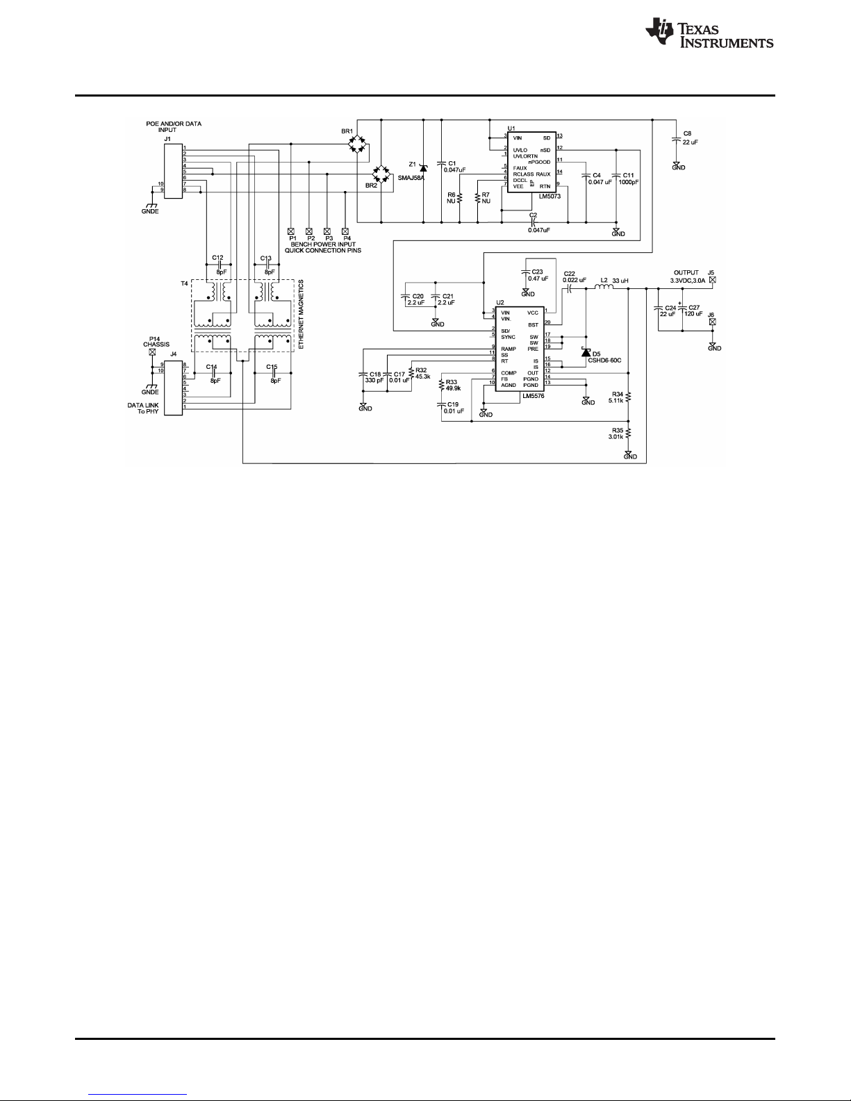
19 The Complete Evaluation Board Schematic
The Complete Evaluation Board Schematic
Figure 10. The Complete Schematic of the Evaluation Board
SNVA214A–April 2007–Revised April 2013 AN-1574 LM5073 Evaluation Board
Submit Documentation Feedback
Figure 11. Silkscreen
13
Copyright © 2007–2013, Texas Instruments Incorporated
Page 14

The Complete Evaluation Board Schematic
www.ti.com
Figure 12. Top Layer
14
AN-1574 LM5073 Evaluation Board SNVA214A–April 2007–Revised April 2013
Copyright © 2007–2013, Texas Instruments Incorporated
Submit Documentation Feedback
Page 15

www.ti.com
Bill of Materials
20 Bill of Materials
ITEM PART NUMBER DESCRIPTION VALUE
BR1 CBR1-D020S DIODE BRIDGE, SMDIP, CENTRAL 1A, 200V
BR2 CBR1-D020S DIODE BRIDGE, SMDIP, CENTRAL 1A, 200V
C1 C3216X7R2A473K CAPACITOR, CER, CC1206, TDK 0.047µF, 100V
C2 C3216X7R2A473K CAPACITOR, CER, CC1206, TDK 0.047µF, 100V
C3 NU NOT POPULATED
C4 C0805C473K5RAC CAPACITOR, CER, CC0805, KEMET 0.047µF, 50V
C5 NU NOT POPULATED
C6 NU NOT POPULATED
C7 NU NOT POPULATED
C8 EEV-HA2A220P CAPACITOR, AL ELEC, PANASONIC 22µF, 100V
C9 NU NOT POPULATED
C10 NU NOT POPULATED
C11 C2012X5R1C102K CAPACITOR, CER, CC0805, TDK 1000pF, 100V
C12 C0805C473K5RAC CAPACITOR, CER, CC0603, AVX 8pF, 100V
C13 C0805C473K5RAC CAPACITOR, CER, CC0603, AVX 8pF, 100V
C14 C0805C473K5RAC CAPACITOR, CER, CC0603, AVX 8pF, 100V
C15 C0805C473K5RAC CAPACITOR, CER, CC0603, AVX 8pF, 100V
Figure 13. Bottom Layer
Table 6. Bill of Materials
SNVA214A–April 2007–Revised April 2013 AN-1574 LM5073 Evaluation Board
Submit Documentation Feedback
15
Copyright © 2007–2013, Texas Instruments Incorporated
Page 16

Bill of Materials
ITEM PART NUMBER DESCRIPTION VALUE
C16 C0805C470G1GAC CAPACITOR, CER, CC0805, KEMET 47pF, 100V
C17 C2012X5R1C103K CAPACITOR, CER, CC0805, TDK 0.01µF, 100V
C18 C0805C331G1GAC CAPACITOR, CER, CC0805, KEMET 330pF, 100V
C19 C2012X5R1C103K CAPACITOR, CER, CC0805, TDK 0.01µF, 100V
C20 C4532X7R2A225M CAPACITOR, CER, CC1812, TDK 2.2µF, 100V
C21 C4532X7R2A225M CAPACITOR, CER, CC1812, TDK 2.2µF, 100V
C22 C2012X7R2A223K CAPACITOR, CER, CC0805, TDK 0.022 µF, 100V
C23 C2012X5R1E474M CAPACITOR, CER, CC0805, TDK 0.47µF, 25V
C24 C3325X7R1C226M CAPACITOR, CER, CC1210, TDK 22µF, 16V
C27 APXE6R3ARA121ME61G CAPACITOR, PAS, NIPPON CHEMI-COM 120µF, 6.3V
C28 C2012X5R1E105M CAPACITOR, CER, CC0805, TDK 1µF, 25V
D1 S3BB-13 DIODE, SMB, DIODE INC 3A, 100V
D2 S3BB-13 DIODE, SMB, DIODE INC 3A, 100V
D3 NU NOT POPULATED
D4 SHORT-LEADS SHORT WITH R1206 0 OHM RES OR
D5 CHSD6-60C DIODE, DPAK, CENTRAL 6A, 60V
D6 NU NOT POPULATED
D7 CMHD4448 DIODE, SOD123, CENTRAL 125mA, 75V
J1 CN-PHONE8P8C-RA-SHLD RJ45 CONNECTOR
J2 PJ-102A POWER JACK
J3 PJ-102A POWER JACK
J4 CN-PHONE8P8C-RA-SHLD RJ45 CONNECTOR
J5 3104-2-00-01-00-00-080 POST, MILL MAX
J6 3104-2-00-01-00-00-080 POST, MILL MAX
JMP1 A26542-ND CONN HEADER VERT., 2POS, DIGI-KEY 2 PIN HEADER
JMP2 A26544-ND CONN HEADER VERT., 3POS, DIGI-KEY 3 PIN HEADER
JMP3 A26544-ND CONN HEADER VERT., 3POS, DIGI-KEY 3 PIN HEADER
JMP4 A26544-ND CONN HEADER VERT., 3POS, DIGI-KEY 3 PIN HEADER
JMP5 A26544-ND CONN HEADER VERT., 3POS, DIGI-KEY 3 PIN HEADER
JMP6 A26544-ND CONN HEADER VERT., 3POS, DIGI-KEY 3 PIN HEADER
JMP7 A26542-ND CONN HEADER VERT., 2POS, DIGI-KEY 2 PIN HEADER
JMP8 A26544-ND CONN HEADER VERT., 3POS, DIGI-KEY 3 PIN HEADER
JMP9 A26542-ND CONN HEADER VERT., 2POS, DIGI-KEY 2 PIN HEADER
JMP11 A26542-ND CONN HEADER VERT., 2POS, DIGI-KEY 2 PIN HEADER
JMP12 A26542-ND CONN HEADER VERT., 2POS, DIGI-KEY 2 PIN HEADER
JMP13 A26542-ND CONN HEADER VERT., 2POS, DIGI-KEY 2 PIN HEADER
L1 DO3308P-682MLD SM INDUCTOR, COILCRAFT 6.8uH
L2 DR127-330 INDUCTOR, COOPER 33uH
LED1 SSL-LXA228GC-TR11 LED,GREEN, LUMEX
P1 3104-2-00-01-00-00-080 POST, MILL MAX
P2 3104-2-00-01-00-00-080 POST, MILL MAX
P3 3104-2-00-01-00-00-080 POST, MILL MAX
P4 3104-2-00-01-00-00-080 POST, MILL MAX
P5 3104-2-00-01-00-00-080 POST, MILL MAX
P6 3104-2-00-01-00-00-080 POST, MILL MAX
P7 3104-2-00-01-00-00-080 POST, MILL MAX
P8 3104-2-00-01-00-00-080 POST, MILL MAX
www.ti.com
Table 6. Bill of Materials (continued)
BUS WIRE
16
AN-1574 LM5073 Evaluation Board SNVA214A–April 2007–Revised April 2013
Submit Documentation Feedback
Copyright © 2007–2013, Texas Instruments Incorporated
Page 17

www.ti.com
Bill of Materials
Table 6. Bill of Materials (continued)
ITEM PART NUMBER DESCRIPTION VALUE
P9 3104-2-00-01-00-00-080 POST, MILL MAX
P10 3104-2-00-01-00-00-080 POST, MILL MAX
P11 3104-2-00-01-00-00-080 POST, MILL MAX
P12 3104-2-00-01-00-00-080 POST, MILL MAX
P13 3104-2-00-01-00-00-080 POST, MILL MAX
P14 3104-2-00-01-00-00-080 POST, MILL MAX
P15 3104-2-00-01-00-00-080 POST, MILL MAX
Q1 NU NOT POPULATED
Q2 NU NOT POPULATED
R1 CRCW08050R0J RESISTOR 0 Ohm
R2 NU NOT POPULATED
R3 CRCW08050R0J RESISTOR 0 Ohm
R4 CRCW08051002F RESISTOR 10K
R5 NU NOT POPULATED
R6 NU NOT POPULATED
R7 CRCW08051582F RESISTOR 15.8K
R8 CRCW08053013F RESISTOR 301K
R9 CRCW08054991F RESISTOR 4.99K
R10 CRCW08053321F RESISTOR 3.32K
R11 CRCW12062492F RESISTOR 24.9K
R12 CRCW12062492F RESISTOR 24.9K
R13 NU NOT POPULATED
R14 NU NOT POPULATED
R15 NU NOT POPULATED
R16 NU NOT POPULATED
R17 CRCW2512100J RESISTOR 1 Ohm, 1W
R18 CRCW2512100J RESISTOR 1 Ohm, 1W
R25 NU NOT POPULATED
R26 CRCW08051002F RESISTOR 10K
R27 CRCW08051002F RESISTOR 10K
R28 NU NOT POPULATED
R29 NU NOT POPULATED
R32 CRCW08054532F RESISTOR 45.3K
R33 CRCW08054992F RESISTOR 49.9K
R34 CRCW08055111F RESISTOR 5.11K
R35 CRCW08053011F RESISTOR 3.01K
R36 NU NOT POPULATED
T1 SHORT LEADS SHORT LEADS ON EACH SIDE (1-2, 3-4) AWG18 BUS WIRE
T4 ETH1-230LD XFMR, POE+ETHERNET, COILCRAFT
U1 LM5073 PD INTERFACE, NSC
U2 LM5576 REGULATOR, NSC
Z1 SMAJ58A TVS, 58V, SMA, DIODE INC
Z2 NU NOT POPULATED
Z3 NU NOT POPULATED
SNVA214A–April 2007–Revised April 2013 AN-1574 LM5073 Evaluation Board
Submit Documentation Feedback
17
Copyright © 2007–2013, Texas Instruments Incorporated
Page 18

Bill of Materials
ITEM PART NUMBER DESCRIPTION VALUE
C7 C2012X5R1E474M CAPACITOR, CER, CC0805, TDK 0.47µF, 25V
C9 1808JA250102MCTPY2 CAPACITOR, Y-TYPE, SYFER 1000pF, 250Vac
C10 1808JA250102MCTPY2 CAPACITOR, Y-TYPE, SYFER 1000pF, 250Vac
D3 CMHD4448 DIODE, SOD123, CENTRAL 125mA, 75V
D6 CMHD4448 DIODE, SOD123, CENTRAL 125mA, 75V
Q1 CMPT2222A BIPOLAR, NPN, SOT-23, CENTRAL 0.6A, 60V
Q2 SI4470EY MOSFET, N-CH, SO-8, VISHAY 12A, 60V
R13 CRCW1206100RJ RESISTOR 100Ω
R14 CRCW12062001F RESISTOR 2.0K
R15 CRCW08051003F RESISTOR 100K
R16 CRCW08051004F RESISTOR 100k
T1 D1882-AL COMMOM-MODE CHOKE, COILCRAFT 1.5mH
Z3 CMPZ524B ZENER, SOT-23, CENTRAL 10V
www.ti.com
Table 7. BOM for Additional Features
18
AN-1574 LM5073 Evaluation Board SNVA214A–April 2007–Revised April 2013
Copyright © 2007–2013, Texas Instruments Incorporated
Submit Documentation Feedback
Page 19

IMPORTANT NOTICE
Texas Instruments Incorporated and its subsidiaries (TI) reserve the right to make corrections, enhancements, improvements and other
changes to its semiconductor products and services per JESD46, latest issue, and to discontinue any product or service per JESD48, latest
issue. Buyers should obtain the latest relevant information before placing orders and should verify that such information is current and
complete. All semiconductor products (also referred to herein as “components”) are sold subject to TI’s terms and conditions of sale
supplied at the time of order acknowledgment.
TI warrants performance of its components to the specifications applicable at the time of sale, in accordance with the warranty in TI’s terms
and conditions of sale of semiconductor products. Testing and other quality control techniques are used to the extent TI deems necessary
to support this warranty. Except where mandated by applicable law, testing of all parameters of each component is not necessarily
performed.
TI assumes no liability for applications assistance or the design of Buyers’ products. Buyers are responsible for their products and
applications using TI components. To minimize the risks associated with Buyers’ products and applications, Buyers should provide
adequate design and operating safeguards.
TI does not warrant or represent that any license, either express or implied, is granted under any patent right, copyright, mask work right, or
other intellectual property right relating to any combination, machine, or process in which TI components or services are used. Information
published by TI regarding third-party products or services does not constitute a license to use such products or services or a warranty or
endorsement thereof. Use of such information may require a license from a third party under the patents or other intellectual property of the
third party, or a license from TI under the patents or other intellectual property of TI.
Reproduction of significant portions of TI information in TI data books or data sheets is permissible only if reproduction is without alteration
and is accompanied by all associated warranties, conditions, limitations, and notices. TI is not responsible or liable for such altered
documentation. Information of third parties may be subject to additional restrictions.
Resale of TI components or services with statements different from or beyond the parameters stated by TI for that component or service
voids all express and any implied warranties for the associated TI component or service and is an unfair and deceptive business practice.
TI is not responsible or liable for any such statements.
Buyer acknowledges and agrees that it is solely responsible for compliance with all legal, regulatory and safety-related requirements
concerning its products, and any use of TI components in its applications, notwithstanding any applications-related information or support
that may be provided by TI. Buyer represents and agrees that it has all the necessary expertise to create and implement safeguards which
anticipate dangerous consequences of failures, monitor failures and their consequences, lessen the likelihood of failures that might cause
harm and take appropriate remedial actions. Buyer will fully indemnify TI and its representatives against any damages arising out of the use
of any TI components in safety-critical applications.
In some cases, TI components may be promoted specifically to facilitate safety-related applications. With such components, TI’s goal is to
help enable customers to design and create their own end-product solutions that meet applicable functional safety standards and
requirements. Nonetheless, such components are subject to these terms.
No TI components are authorized for use in FDA Class III (or similar life-critical medical equipment) unless authorized officers of the parties
have executed a special agreement specifically governing such use.
Only those TI components which TI has specifically designated as military grade or “enhanced plastic” are designed and intended for use in
military/aerospace applications or environments. Buyer acknowledges and agrees that any military or aerospace use of TI components
which have not been so designated is solely at the Buyer's risk, and that Buyer is solely responsible for compliance with all legal and
regulatory requirements in connection with such use.
TI has specifically designated certain components as meeting ISO/TS16949 requirements, mainly for automotive use. In any case of use of
non-designated products, TI will not be responsible for any failure to meet ISO/TS16949.
Products Applications
Audio www.ti.com/audio Automotive and Transportation www.ti.com/automotive
Amplifiers amplifier.ti.com Communications and Telecom www.ti.com/communications
Data Converters dataconverter.ti.com Computers and Peripherals www.ti.com/computers
DLP® Products www.dlp.com Consumer Electronics www.ti.com/consumer-apps
DSP dsp.ti.com Energy and Lighting www.ti.com/energy
Clocks and Timers www.ti.com/clocks Industrial www.ti.com/industrial
Interface interface.ti.com Medical www.ti.com/medical
Logic logic.ti.com Security www.ti.com/security
Power Mgmt power.ti.com Space, Avionics and Defense www.ti.com/space-avionics-defense
Microcontrollers microcontroller.ti.com Video and Imaging www.ti.com/video
RFID www.ti-rfid.com
OMAP Applications Processors www.ti.com/omap TI E2E Community e2e.ti.com
Wireless Connectivity www.ti.com/wirelessconnectivity
Mailing Address: Texas Instruments, Post Office Box 655303, Dallas, Texas 75265
Copyright © 2013, Texas Instruments Incorporated
 Loading...