

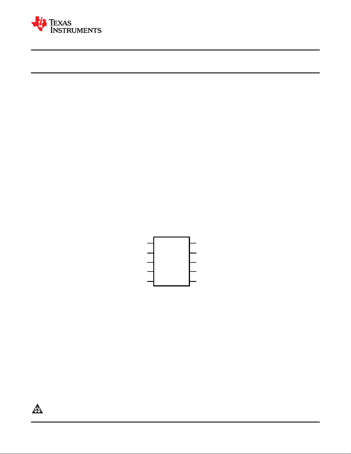
OUT2
GND
CS
RT/SYNC
1
2
3
4
5
6
7
8
9
10
REF
V
CC
OUT1
V
IN
COMP
SS
LM5033
www.ti.com
LM5033 100V Push-Pull Voltage Mode PWM Controller
1
FEATURES
2
• Internal High Voltage (100V) Start-Up
Regulator
• Single Resistor Oscillator Setting
• Synchronizable
• Precision Reference Output
• Adjustable Soft-Start
• Over-Current Protection
• Direct Optocoupler Interface
• 1.5A Peak Gate Drivers
• Thermal Shutdown
APPLICATIONS
• Intermediate DC/DC Bus Converter
• Telecommunication Power Converters
• Industrial Power Converters
• +42V Automotive Systems
SNVS181B –APRIL 2004–REVISED APRIL 2013
Check for Samples: LM5033
PACKAGE
• VSSOP-10
• WSON-10
DESCRIPTION
The LM5033 High Voltage PWM controller contains
all the features needed to implement Push-Pull, HalfBridge, and Full-Bridge topologies. Applications
include closed loop voltage mode converters with a
highly regulated output voltage, or an open loop "DC
transformer" such as an Intermediate Bus Converter
(IBC) with an efficiency >95%. Two alternating gate
driver outputs with a specified deadtime are provided.
The LM5033 includes a start-up regulator that
operates over a wide input range of 15V to 100V.
Additional features include: precision voltage
reference output, current limit detection, remote
shutdown, softstart, sync capability and thermal
shutdown. This high speed IC has total propagation
delays less than 100 ns and a 1MHz capable
oscillator.
Connection Diagram
Figure 1. 10-Lead VSSOP, WSON
Package Number DGS0010A, DPR0010A
1
2All trademarks are the property of their respective owners.
PRODUCTION DATA information is current as of publication date.
Products conform to specifications per the terms of the Texas
Instruments standard warranty. Production processing does not
necessarily include testing of all parameters.
Please be aware that an important notice concerning availability, standard warranty, and use in critical applications of
Texas Instruments semiconductor products and disclaimers thereto appears at the end of this data sheet.
Copyright © 2004–2013, Texas Instruments Incorporated
LM5033
SNVS181B –APRIL 2004–REVISED APRIL 2013
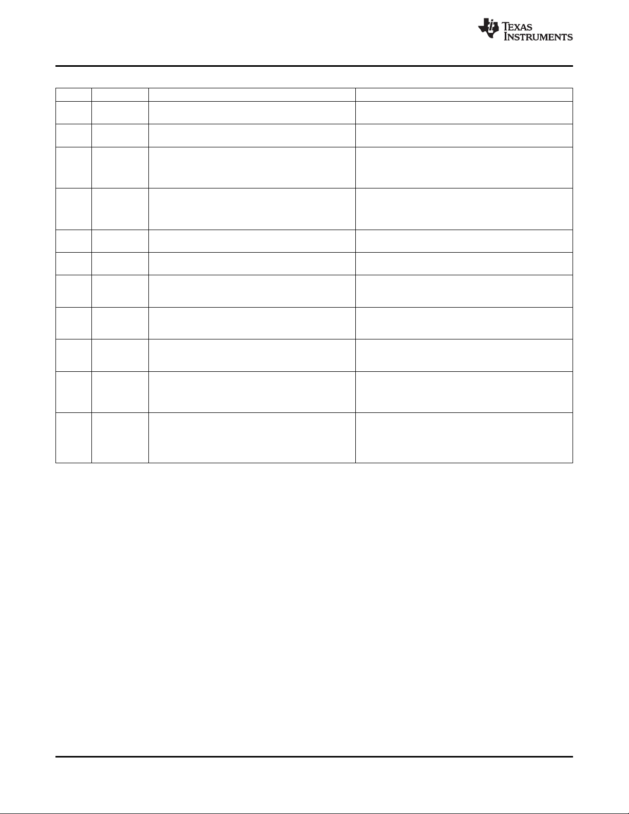
PIN DESCRIPTIONS
PIN NAME DESCRIPTION APPLICATION INFORMATION
1 Vin Input Voltage Input to the start-up regulator. Input range is 15V to 90V,
with transient capability to 100V .
2 REF 2.5V precision reference output Sink only, requires an external pull-up resistor. This can
be used as a reference for external circuitry.
3 COMP PWM Input Feedback to the PWM comparator’s inverting input,
through a 3:1 divider. The output duty cycle increases as
this pin’s voltage increases. Internally there is a 5kΩ
pullup to +5.2V.
4 VCC 9.6V output from the internal high voltage series pass An external voltage (10V - 15V) can be applied to this pin
regulator to shutdown the internal regulator, thereby reducing
internal dissipation. An internal diode connects Vcc to
Vin.
5 OUT1 Gate Driver Output #1 Alternating output gate driver, which can source and sink
1.5A.
6 OUT2 Gate Driver Output #2 Alternating output gate driver, which can source and sink
1.5A.
7 GND Ground pin for all internal circuitry Connections to external ground must be done with care
for optimum performance. See the Functional Description
and Application Information Section for more information.
8 CS Current sense input Current sense input for the current limit detection. If CS
exceeds 0.5V the outputs are disabled and the softstart
pin is discharged to ground.
9 RT/ SYNC Oscillator timing resistor pin and synchronization input An external resistor to ground sets the oscillator
frequency. This pin will also accept ac-coupled
synchronization pulses from an external source.
10 SS Softstart pin An internal 10µA current source and an external
capacitor set the soft-start timing. This pin can be
externally pulled to below 0.5V to disable the output
drivers.
WSON SUB Die Substrate The exposed die attach pad on the WSON package
DAP should be connected to a PCB thermal pad at ground
potential. For additional information on using Texas
Instruments's No Pull Back WSON package, please refer
to Application Note AN-1187.
www.ti.com
2 Submit Documentation Feedback Copyright © 2004–2013, Texas Instruments Incorporated
Product Folder Links: LM5033
UNDERVOLTAGE
SENSOR
OSC
REF (2)
(1) V
IN
VCC (4)
(8) CS
0.5V
OUT1 (5)
OUT2 (6)
GND (7)
REFERENCE
GENERATOR
RAMP
GENERATOR
DRIVER
DRIVER
PWM
5k
5.2V
(9) Rt /Sync
SS
0.65V
10k
5k
CLK
(10) SS
(3) COMP
2.5V
10 PA
V
CC
V
CC
2.5V
0.5V
0V
5.0V
9.6V SERIES
REGULATOR
START UP
CIRCUIT
THERMAL
SHUTDOWN
SENSOR
Disable
SS
Offset
4.9V
5.2V
LOGIC
Current Sense
+
-
+
-
+
-
RSQ
Q
CLR
SET
C
DQQ
LM5033
www.ti.com
Block Diagram
SNVS181B –APRIL 2004–REVISED APRIL 2013
These devices have limited built-in ESD protection. The leads should be shorted together or the device placed in conductive foam
during storage or handling to prevent electrostatic damage to the MOS gates.
Figure 2. Functional Block Diagram
Product Folder Links: LM5033
Copyright © 2004–2013, Texas Instruments Incorporated Submit Documentation Feedback 3
LM5033
SNVS181B –APRIL 2004–REVISED APRIL 2013
Absolute Maximum Ratings
(1)(2)
www.ti.com
VINto GND -0.3V to 100V
VCCto GND -0.3V to 16V
Rt/Sync to GND -0.3V to 5.5V
Pins 3, 8, 10 to GND -0.3V to 7.0V
ESD Rating
(3)
Human Body Model 2kV
Storage Temperature Range -65°C to 150°C
Junction Temperature 150°C
Power Dissipation
(4)
Internally Limited
(1) Absolute Maximum Ratings are limits beyond which damage to the device may occur. Operating Ratings are conditions under which
operation of the device is intended to be functional. For specifications and test conditions, see the Electrical Characteristics.
(2) If Military/Aerospace specified devices are required, please contact the Texas Instruments Sales Office/ Distributors for availability and
specifications.
(3) The human body model is a 100 pF capacitor discharged through a 1.5kΩ resistor into each pin.
(4) The maximum allowable power dissipation is a function of the maximum allowed junction temperature (T
(TA), and the junction-to-ambient thermal resistance (θJA). The maximum allowable power dissipation can be calculated from PD =
(T
- TA) / θJA. Excessive power dissipation will cause the thermal shutdown to activate.
J(max)
Operating Ratings
(5)
), the ambient temperature
J(max)
VINVoltage (Pin1) 15 to 90V
Operating Junction Temperature -40°C to 125°C
(5) Absolute Maximum Ratings are limits beyond which damage to the device may occur. Operating Ratings are conditions under which
operation of the device is intended to be functional. For specifications and test conditions, see the Electrical Characteristics.
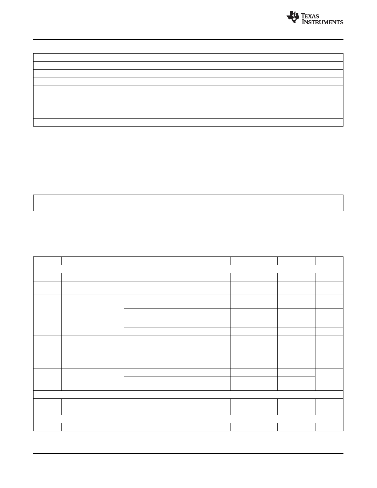
Electrical Characteristics
Specifications with standard typeface are for TJ= 25°C, and those with boldface type apply over full Operating Junction
Temperature range. VIN= 48V, VCC= 10V applied externally, RT= 26.7kΩ, unless otherwise stated. See
Symbol Parameter Conditions Min Typ Max Units
VCCStartup Regulator (Pins 1, 4)
VCCReg VCCVoltage Pin 4 open 9.2 9.6 10.0 V
Icc-out VCCCurrent Limit Out1, Out2 disabled. Ext. 20 34 mA
Iin Startup Regulator Current Normal Operation 150 500 µA
into V
IN
UVT VCCUndervoltage VccReg - VccReg - 100 mV V
Threshold (increasing 300mV
VCC)
UVT Hysteresis 2.3 2.8 3.3
(decreasing VCC)
Icc-in Supply Current from SS Pin = 0V 2 3 mA
external source to V
2.5V Reference (Pin 2)
Vref Output voltage Pin 2 sink current = 5mA 2.44 2.50 2.56 V
Current sink capability 5.0 13 mA
Current Sense (Pin 8)
CS Threshold voltage 0.45 0.50 0.55 V
supply to Vcc disconnected.
VIN= 90V
Ext. VCCSupply 7 mA
Disconnected and Output
Load = 1800pF
SS Pin = 0V 3 mA
CC
SS Pin = open and Output 7
Load = 1800pF
(1)
(2)
and
.
(1) Min and Max limits are 100% production tested at 25°C. Limits over the operating temperature range are specified through correlation
using Statistical Quality Control (SQC) methods. Limits are used to calculate TI’s Average Outgoing Quality Level (AOQL).
(2) Typical specifications represent the most likely parametric norm at 25°C operation.
4 Submit Documentation Feedback Copyright © 2004–2013, Texas Instruments Incorporated
Product Folder Links: LM5033
LM5033
www.ti.com
SNVS181B –APRIL 2004–REVISED APRIL 2013
Electrical Characteristics (continued)
Specifications with standard typeface are for TJ= 25°C, and those with boldface type apply over full Operating Junction
Temperature range. VIN= 48V, VCC= 10V applied externally, RT= 26.7kΩ, unless otherwise stated. See
Symbol Parameter Conditions Min Typ Max Units
CS delay to output Pin 8 taken from zero to 30 ns
Current sink capability Pin 8 ≤ 0.3V 3 6 mA
(clocked)
Softstart (Pin 10)
Softstart current source 7 10 13 µA
Softstart to Comp offset 0.25 0.50 0.75 V
Open Circuit Voltage 5.0 V
Oscillator (Pin 9)
Fs1 Internal frequency Rt = 26.7 kΩ 175 200 225 kHz
Fs2 Internal frequency Rt = 8.2 kΩ 600 kHz
Vsync Sync threshold 3.2 3.8 V
Rt/Sync DC voltage 2.0 V
PWM Comparator Input (Pin 3)
t
PWM
Gain from pin 3 to PWM 0.34 V/V
comparator
Maximum duty cycle at See PWM Comparator text 100 x (0.5TS- %
Out1, Out2 TD)/T
Minimum duty cycle at Pin 3 = 0V. 0 %
Out1, Out2
Open Circuit Voltage 4.2 5.2 6.2 V
Short circuit current Pin 3 = 0V 0.6 1.1 1.5 mA
Output Drivers (Pin 5, 6)
Deadtime (TD) CLoad = 0 @ OUT1, OUT2. 85 135 185 ns
Rise Time C
Fall Time C
Output High Voltage Iout = 50 mA (source) Vcc-0.75 Vcc-0.25 V
Output Low Voltage Iout = 100 mA (sink) 0.25 0.75 V
Max. source current 1.5 A
Max. sink current 1.5 A
Thermal Shutdown
T
SD
Shutdown temperature 165 °C
Shutdown temperature 15 °C
hysteresis
Thermal Resistance
θ
JA
Junction to Ambient DGS0010A Package 200 °C/W
0.6V. Time for Out1 or Out2
to fall to 90% of Vcc. CLoad
= 0 @ Out1, Out2
S
Time measured from 10% of
falling output to 10% of rising
output.
= 1nF 16 ns
Load
= 1nF 16 ns
Load
DPR0010A Package 38
(1)
(2)
and
.
Copyright © 2004–2013, Texas Instruments Incorporated Submit Documentation Feedback 5
Product Folder Links: LM5033
125
130
135
140
145
150
155
-50 0 50 100 150
DEADTIME (ns)
TEMPERATURE (oC)
-50 0 50 100 150
9.4
9.6
9.8
10.0
10.2
10.4
I
SS
(PA)
TEMPERATURE (oC)
-50 0 50 100 150 200
198
199
200
201
202
OSCILLATOR FREQUENCY (kHz)
TEMPERATURE (oC)
1
1000
100
RT (k:)
10 100
OSCILLATOR FREQUENCY (kHz)
0 2 4 6 8 10 12 14 16
VIN (V)
0
2
4
6
8
10
12
14
16
V
CC
(V)
VCC not externally powered
0 5 10 15 20 25 30 35 40
ICC (mA)
0
2
4
6
8
10
12
14
16
V
CC
(V)
LM5033
SNVS181B –APRIL 2004–REVISED APRIL 2013
V
CC
vs vs
V
IN
Figure 3. Figure 4.
Oscillator Frequency vs
vs Temperature
R
T
Typical Performance Characteristics
V
CC
ICC(VIN= 48V)
Oscillator Frequency
RT= 26.7kΩ
www.ti.com
6 Submit Documentation Feedback Copyright © 2004–2013, Texas Instruments Incorporated
Figure 5. Figure 6.
Soft Start Current Dead Time
vs vs
Temperature Temperature
Figure 7. Figure 8.
Product Folder Links: LM5033
0 20 40 60 80 100
0
2
4
6
8
10
I
IN
(mA)
VIN (V)
Output Load = 1500 pF
Pin 10 = 0V
Output Load = 0 pF
10 11 12 13 14 15
0
2
4
6
8
10
12
I
CC
(mA)
VCC (V)
Output Load = 1500 pF
Output Load = 0
SS Pin = 0V
0 5 10 15 20 25
0
0.5
1.0
1.5
2.0
2.5
3.0
3.5
V
REF
(V)
I
REF
(mA)
0 1.0 2.0 3.0 4.0 5.0
0
10
20
30
40
50
OUTPUT DUTY CYCLE (%)
COMP PIN VOLTAGE - PIN 3 (V)
LM5033
www.ti.com
SNVS181B –APRIL 2004–REVISED APRIL 2013
Typical Performance Characteristics (continued)
Output Duty Cycle
(VCCPowered Externally) (VCCNot Powered Externally)
vs V
Comp Voltage vs
RT= 16.5kΩ I
REF
Figure 9. Figure 10.
I
CC
vs vs
V
CC
I
V
REF
IN
IN
Copyright © 2004–2013, Texas Instruments Incorporated Submit Documentation Feedback 7
Figure 11. Figure 12.
Product Folder Links: LM5033

LM5033
SNVS181B –APRIL 2004–REVISED APRIL 2013
www.ti.com
FUNCTIONAL DESCRIPTION
The LM5033 High Voltage PWM controller contains all of the features needed to implement Push-Pull and Bridge
topologies, using voltage-mode control in a small 10 pin package. Features included are: startup regulator,
precision 2.5V reference output, current limit detection, alternating gate drivers, sync capability, thermal
shutdown, softstart, and remote shutdown. This high speed IC has total propagation delays <100 ns. These
features simplify the design of an open loop DC-DC converter, or a voltage controlled closed loop converter. The
Functional Block Diagram is shown in Figure 2.
High Voltage Start-Up Regulator (Pins 1, 4)
The LM5033 contains an internal high voltage startup regulator. The input pin (VIN) can be connected directly to
line voltages as high as 90V for normal operation, and can withstand transients to 100V. The regulator output at
VCC(9.6V) is internally current limited and sources a minimum of 20mA. Upon power up, the capacitor at VCCwill
charge up, providing a time delay while internal circuits stabilize. When VCCreaches the upper threshold of the
under-voltage sensor (typically 9.5V), the under-voltage sensor resets, enabling the output drivers, although the
PWM duty cycle will initially be at zero. As the Softstart capacitor then charges up (described below) the output
duty cycle will increase until regulated by the PWM control loop. The value of the VCCcapacitor which affects the
above mentioned delay depends on the total system design and its start-up characteristics. The recommended
range of values for the VCCcapacitor is 0.1 to 50µF.
The lower threshold of the under-voltage sensor is typically at 6.8V. If VCCfalls below this value the outputs are
disabled and the softstart capacitor is discharged. When VCCis again increased above the upper threshold the
outputs are enabled, and the softstart sequence repeats.
The LM5033’s internal power dissipation can be reduced by powering VCCfrom an external supply. Typically this
is done by means of an auxiliary transformer winding which is diode connected to the VCCpin to provide 10-15V
to VCCas the controller completes the start-up sequence. The externally applied VCCvoltage will cause the
internal regulator to shut off. The under-voltage sensor circuit will still function in this mode, requiring that the
external VCCcapacitor be sized so that VCCnever falls below 6.8V. The required current into the VCCpin from the
external source is shown in Typical Performance Characteristics (ICCvs. VCC).
If a fault condition occurs such that the external supply to VCCfails, external current draw from the VCCpin must
be limited as to not exceed the regulator’s current limit, or the maximum power dissipation of the IC. An external
start-up or other bias rail can be used instead of the internal start-up regulator by connecting the VCCand the V
pins together and feeding the external bias voltage (10-15V) into that node.
A thermal shutdown protection will activate if the die temperature exceeds 165ºC, disabling the outputs (OUT1
and OUT2), and shutting down the VCCregulator. When the die temperature has reduced below 150°C (typical
hysteresis = 15°C) the VCCregulator is enabled and a softstart sequence will initiate.
IN
Reference (Pin 2)
The Ref pin provides a reference voltage of 2.5V, ±2.4%. The pin is internally connected to an NMOS FET drain
at the buffer amplifier’s output, allowing it to sink, but not source current. An external pullup resistor is required.
Current into the pin must be limited to less than 20 mA to maintain regulation. See the graph in the Typical
Performance Characteristics.
During start-up if the pullup voltage is present before the reference amplifier establishes regulation, the voltage
on pin 2 must not exceed 5.5V. If this reference is not used the Ref pin can float or be connected to ground.
PWM Comparator (Pin 3), Duty Cycle and Deadtime
The PWM comparator compares an internal ramp signal (0 - 0.65V) with the loop error voltage derived from the
Comp pin (pin 3). The Comp voltage is typically set by an external error amplifier through an optocoupler for
closed loop applications. Internally, the voltage at the Comp pin passes through two level shifting diodes, and a
gain reducing 3:1 resistor divider. The output of the PWM comparator provides the pulse width information to the
output drivers (Out1 and Out2). This comparator is optimized for speed in order to achieve minimum discernable
duty cycles. The output duty cycle is 0% for V
Performance Characteristics. The maximum duty cycle for each output is limited to less than 50% due to the
forced deadtime. The typical deadtime between the falling edge of one gate driver output and the rising edge of
the other gate driver output is 135 ns, and does not vary with frequency. The maximum duty cycle for each
output can be calculated from:
8 Submit Documentation Feedback Copyright © 2004–2013, Texas Instruments Incorporated
Product Folder Links: LM5033
< 1.5V, and maximum for V
COMP
> 3.5V. See the Typical
COMP

Rt =
(1/F) - 172*10
-9
182*10
-12
DC =
(0.5 x TS) - T
D
T
S
LM5033
www.ti.com
SNVS181B –APRIL 2004–REVISED APRIL 2013
where
• TSis the period of each output
• TDis the deadtime (1)
For example, if the oscillator frequency is 200 kHz, each output will cycle at 100 kHz, and TS= 10 µs. Using the
nominal deadtime of 135 ns, the maximum duty cycle at this frequency is 48.65%. Using the minimum deadtime
of 85 ns, the maximum duty cycle increases to 49.15%.
When the Softstart pin (pin 10) is pulled down (internally or externally) the Comp pin voltage is pulled down with
it, with a difference of 0.5V. When the Softstart pin voltage increases the Comp voltage is allowed to increase,
pulled up by an internal 5.2V supply through a 5kΩ resistor.
In an open loop application, such as an intermediate bus converter, pin 3 can be left open resulting in maximum
duty cycle at the output drivers .
Current Sense (Pin 8)
The current sense circuit is intended to protect the power converter when an abnormal primary current is sensed
by initiating a low duty cycle hiccup mode. When the threshold (0.5V) at Pin 8 is exceeded the outputs are
disabled, and the softstart capacitor (at pin 10) is internally discharged. When the softstart capacitor is fully
discharged and the voltage at the CS pin is below 0.5V, the outputs are re-enabled allowing the softstart
capacitor voltage and the output duty cycle to increase.
The external current sensing circuit should include an RC filter located near the IC to prevent false triggering of
the Current Sense comparator due to transients or noise. An internal MOSFET discharges the external filter
capacitor at the conclusion of each PWM cycle to improve dynamic performance. The discharge time is equal to
the deadtime between Out1 and Out2 at maximum duty cycle. Additionally, pin 8 is pulled low when VCCis below
the under-voltage threshold or when an over temperature condition occurs.
Oscillator, Sync Capability (Pin 9)
The LM5033 oscillator frequency is set by a single external resistor connected between Rt/Sync and ground. The
required Rt resistor is calculated from:
(2)
The outputs (Out1 and Out2) alternate at half the oscillator frequency. The voltage at the Rt/Sync pin is internally
regulated to a nominal 2.0V. The Rt resistor should be located as close as possible to the IC, and connected
directly to the pins (Rt and GND).
The LM5033 can be synchronized to an external clock by applying a narrow pulse to pin 9. The external clock
must be a higher frequency than the free running frequency set by the Rt resistor, and the pulse width must be
between 15 and 150 ns. The clock signal must be coupled into the Rt/Sync pin through a 100 pF capacitor.
When the synchronizing pulse transitions low-to-high, the voltage at pin 9 must exceed 3.8V from its nominal
2.0V dc level. During the clock signal’s low time the voltage at pin 9 will be clamped at 2.0V by an internal
regulator. The Rt resistor is always required, whether the oscillator is free running or externally synchronized.
Soft Start (Pin 10)
The softstart feature allows the converter to gradually reach a steady state operating point, thereby reducing
start-up stresses and current surges. Upon turn-on, after the under-voltage sensor resets at VCC, an internal 10
µA current source charges an external capacitor at pin 10 to generate a ramping voltage (0 to + 5V) which allows
the voltage on the Comp pin (pin 3) to increase gradually. As the COMP voltage increases the output duty cycle
will increase from zero to the value required for regulation. Internally, the softstart pin is pulled low when a
current fault is detected at pin 8, the VCCvoltage is below the lower threshold of the under-voltage sensor, or
when a thermal shutdown occurs. Additionally, the softstart pin can be pulled low by an external device.
Copyright © 2004–2013, Texas Instruments Incorporated Submit Documentation Feedback 9
Product Folder Links: LM5033

LM5033
SNVS181B –APRIL 2004–REVISED APRIL 2013
www.ti.com
In the event of a current fault, (see Current Sense section) the softstart capacitor will be discharged by an
internal pull-down device. The falling voltage at pin 10 will pull down the COMP pin, thereby ensuring a minimum
output duty cycle when the outputs are re-enabled. The softstart capacitor will then begin to ramp up, allowing
the COMP voltage to increase. As the COMP voltage increases, the output duty cycle increases from zero to the
value required for regulation. However, if the fault condition is still present the above sequence repeats until the
fault is removed.
If the VCCvoltage falls below the lower under-voltage sensor threshold (typically 6.8V) the outputs are disabled,
and the softstart capacitor is discharged. The falling voltage at pin 10 will pull down the COMP pin, thereby
ensuring minimum output duty cycle when the outputs are re-enabled. After the VCCvoltage increases above the
upper threshold (typically 9.5V), the outputs are enabled, and the softstart capacitor will begin to ramp up,
allowing the COMP pin voltage to increase. The output duty cycle will then increase from zero to the value
required for regulation.
In the event of a fault which results in an excessively high die temperature, an internal Thermal Shutdown circuit
is provided to protect the IC. When activated (at 165°C) the IC is forced into a low power reset state, disabling
the output drivers and the VCCregulator. When the die temperature has reduced (typical hysteresis = 15°C), the
VCCregulator is enabled and a softstart sequence will initiate.
Using an externally controlled switch, the outputs (Pins 5 & 6) can be disabled at any time by pulling pin 10
below 0.5V. This will pull down the COMP pin to near ground, causing the output duty cycle to go to zero. Upon
releasing pin 10, the softstart capacitor will ramp up, allowing the COMP pin voltage to increase. The output duty
cycle then increases from zero to the value required for regulation.
OUT1, OUT2 (Pins 5, 6)
The LM5033 provides two alternating outputs, OUT1 and OUT2, each capable of sourcing and sinking 1.5A
peak. Each will toggle at one-half the internal oscillator frequency. The voltage output levels are nominally
ground and VCC, minus a saturation voltage at each level which depends on the current flow.
The outputs can drive power MOSFETs directly in a push-pull application, or they can drive a high voltage gate
driver (e.g., LM5100) in a bridge application.
The outputs are disabled when any of the following conditions occur:
1. An overcurrent condition is detected at pin 8,
2. The VCCunder-voltage sensor is active,
3. An over-temperature condition is detected, or
4. The voltage at Pin 10 is below 0.5V
Thermal Protection
The system design should limit the LM5033 junction temperature to not exceed 125°C during normal operation.
However, in the event of a fault which results in a higher die temperature, an internal Thermal Shutdown circuit is
provided to protect the IC. When thermal shutdown is activated, typically at 165°C, the IC is forced into a low
power reset state disabling the output drivers and the VCCregulator. This feature helps prevent catastrophic
failures from accidental device overheating. When the die temperature has reduced (typical hysteresis = 15°C)
the VCCregulator is enabled and a softstart sequence initiates.
Application Information
The following information is intended to provide guidelines for implementing the LM5033. However, final selection
of all external components is dependent on the configuration and operating characteristics of the complete power
conversion system.
VIN(PIN 1)
The voltage applied at pin 1, normally the same as that applied to the main transformer’s primary, can be in the
range of 15 to 90V, with transient capability to 100V. The current into pin 1 depends not only on VIN, but also on
the load on the output driver pins, any load on VCC, and whether or not an external voltage is applied to VCC. If
Vin is close to the absolute maximum rating of the LM5033, it is recommended the circuit of Figure 13 be used to
filter transients which may occur at the input supply.
10 Submit Documentation Feedback Copyright © 2004–2013, Texas Instruments Incorporated
Product Folder Links: LM5033

0.1 PF
50
LM5033
V
IN
Supply
Voltage
LM5033
www.ti.com
SNVS181B –APRIL 2004–REVISED APRIL 2013
Figure 13. Input Transient Protection
If VCCis not powered externally, requiring all internal bias currents for the LM5033, and output driver currents, to
be supplied at Vin and through the internal regulator, the required input current (Iin) is shown in the Typical
Performance Characteristics (IINvs. VIN).
If VCCis powered externally, Iin will increase with VINas shown in the above mentioned graph until the external
voltage is applied to VCC. In most applications, this occurs once the outputs are enabled and load current begins
to flow. The current into Vin will then drop to a nominal 150µA (Pin 10 = open or grounded).
VCC(PIN 4)
The capacitor at the VCCpin provides not only noise filtering and stability, but also a necessary time delay during
start-up. The time delay allows the internal circuitry of the LM5033, and associated external circuitry, to stabilize
before VCCreaches its final value, at which time the outputs are enabled and the softstart sequence begins. Any
external circuitry connected to the REF output (Pin 2) and Softstart (Pin 10) should be designed to stabilize
during the time delay.
The current limit of the VCCregulator, and the external capacitor, determine the VCCturn-on time delay. Typically,
a 1µF capacitor will provide approximately 300 µs of delay, with larger capacitors providing proportionately longer
delays. Experimentation with the final design may be necessary to determine the minimum value for the V
CC
capacitor.
SOFTSTART (PIN 10)
The capacitor at pin 10 determines the time required for the output duty cycle to increase from zero to the final
value for regulation. The minimum acceptable time is dependent on the response of the feedback loops to the
COMP pin, as well as the characteristics of the magnetic components. If the Softstart time is too quick, the
system output could significantly overshoot its intended voltage before the loop has a chance to establish
regulation, possibly adversely affecting the load. Experimentation with the final design is usually necessary to
determine the minimum value for the SS capacitor.
CURRENT SENSE (PIN 8)
This pin typically receives an input representative of the primary current from the current sense elements of the
external circuitry. The peak amplitude at this pin must be less than 0.5V for normal operation. Filtering at this pin
should be sufficient to prevent false triggering of the Current Sense comparator, but not significantly delay
detection of an overcurrent condition. The filter’s capacitor at pin 8 should not be larger than 2200 pF.
OSCILLATOR, SYNC INPUT (PIN 9)
The internal oscillator frequency is generally selected in conjunction with the system magnetic components, and
any other aspects of the system which may be affected by the frequency. The Rtresistor at pin 9 sets the
frequency according to the formula in the Functional Description. Each output (OUT1 and OUT2) switches at half
the oscillator frequency. If the required frequency value is critical in a particular application, the tolerance of the
external resistor, and the frequency tolerance indicated in the Electrical Characteristics, must be taken into
account when selecting the resistor.
Copyright © 2004–2013, Texas Instruments Incorporated Submit Documentation Feedback 11
Product Folder Links: LM5033

LM5033
Out1
Out2
LM5100
Hi
Li
LM5033
Out1
Out2
LM5100
Hi
Li
Reduce Deadtime
Increase Deadtime
LM5033
SNVS181B –APRIL 2004–REVISED APRIL 2013
www.ti.com
If the LM5033 is to be synchronized to an external clock, that signal must be coupled into pin 9 through a 100 pF
capacitor. The Rtresistor is still required in this case, and it must be selected to set the internal oscillator to a
frequency lower than the external synchronizing frequency. The amplitude of the external pulses must take pin 9
above 3.8V on the low-to-high transition but no higher than 5.5V. The clock pulse width should be between 15
and 150 ns.
DEADTIME ADJUSTMENT
If the application requires a change in the minimum deadtime between the outputs, the circuits in Figure 14 are
recommended. Suggested values for the resistor and capacitor at each output are 500Ω, and 100 pF,
respectively for a nominal 50 ns change. The diodes can be 1N4148, or similar.
PC BOARD LAYOUT
The LM5033 current sense and PWM comparators are very fast, and as such will respond to short duration noise
pulses. Layout considerations are critical for the current sense filter. The components at pins 3, 8, 9, and 10
should be as physically close as possible to the IC, thereby minimizing noise pickup in the PC tracks.
If a current sense transformer is used both leads of the transformer secondary should be routed to the sense
filter components, and to the IC pins. The ground side of the transformer should be connected via a dedicated
PC board track to pin 7 of the IC rather than through the ground plane.
If the current sense circuit employs a sense resistor in the drive transistor sources, a low inductance resistor
should be used. In this case all the noise sensitive low power grounds should be connected in common near the
IC, and then a single connection made to the power ground (sense resistor ground point).
The outputs of the LM5033, or of the high voltage gate driver (if used), should have short direct paths to the
power MOSFETs in order to minimize the effects of inductance in the PC board traces.
If the internal dissipation of the LM5033 and any of the power devices produces high junction temperatures
during normal operation, good use of the PC board’s ground plane can help considerably to dissipate heat. The
exposed pad on the bottom of the WSON-10 package can be soldered to ground plane on the PC board, and the
ground plane should extend out from beneath the IC to help dissipate the heat. The exposed pad is internally
connected to the IC substrate.
Additionally, the use of wide PC board traces where possible can help conduct heat away from the IC. Judicious
positioning of the PC board within the end product, along with use of any available air flow (forced or natural
convection) can help reduce the junction temperatures.
Figure 14. Deadtime Adjustment
12 Submit Documentation Feedback Copyright © 2004–2013, Texas Instruments Incorporated
Product Folder Links: LM5033

VIN = 60V
VIN = 48V
VIN = 40V
0 5 10 15 20
OUTPUT CURRENT (A)
V
OUT
(V)
6.0
8.0
10.0
12.0
14.0
40V < VIN < 60V
0 5 10 15 20
OUTPUT CURRENT (A)
EFFICIENCY (%)
80
85
90
95
100
LM5033
www.ti.com
SNVS181B –APRIL 2004–REVISED APRIL 2013
APPLICATION CIRCUIT EXAMPLE
Figure 17 shows an example circuit for a half-bridge 200W DC/DC converter built in a quarter brick format. The
circuit is that of an intermediate bus converter (IBC) which operates open-loop (unregulated output), converting a
nominal 48V input to a nominal 9.0V output with a 30 mΩ output impedance. The current sense transformer (T2),
and the associated filter at the CS pin, provide overcurrent detection at approximately 23A. The auxiliary winding
on T1 powers VCCand the LM5100’s V+ pin (once the outputs are enabled) to reduce power dissipation within
the LM5033. The LM5100 provides appropriate level shifting for Q1. Synchronous rectifiers Q3 and Q4 minimize
conduction losses in the output stage. Dual comparators U2 and U3 provide under-voltage and over-voltage
sensing at Vin. The under-voltage sense levels are 37V increasing, and 33V decreasing. The over-voltage sense
levels are 63V increasing, and 61.5V decreasing. The circuit can be shut down by taking the ON/OFF input
below 0.8V. An external synchronizing frequency can be applied to the SYNC input. Measured efficiency and
output characteristics for this circuit are shown in Figure 15 and Figure 16.
Figure 15. Efficiency vs Output Current
Circuit of Figure 17
Figure 16. V
vs Load Current and V
OUT
for the circuit of Figure 17
IN
Copyright © 2004–2013, Texas Instruments Incorporated Submit Documentation Feedback 13
Product Folder Links: LM5033

LM5033
SNVS181B –APRIL 2004–REVISED APRIL 2013
www.ti.com
Figure 17. Intermediate Bus Converter
40V - 60V Input; 7.5 - 11.3V, 20A Output
14 Submit Documentation Feedback Copyright © 2004–2013, Texas Instruments Incorporated
Product Folder Links: LM5033

LM5033
www.ti.com
SNVS181B –APRIL 2004–REVISED APRIL 2013
Table 1. Bill of Materials (for the circuit of Figure 17)
Item Device Package Value
BR1 Schottky diode bridge, Diodes, Inc. SOT-363 30V, 0.2A
C1-4 Capacitor 1812 6.8 µF, 50V
C5 Capacitor 0805 0.47 µF, 25V
C6 Capacitor 0805 0.047 µF, 25V
C7, 12, 16, 20-23 Capacitor 0805 0.1 µF, 16V
C8, 9 Capacitor 0805 470 pF, 50V
C10, 11 Capacitor 1210 22 µF, 16 V
C13 Capacitor 0805 2200 pF, 16V
C14 Capacitor 0805 0.022 µF. 16V
C15, 24 Capacitor 0805 100 pF, 16V
C17 Capacitor 1206 4.7 µF, 16V
C18 Capacitor 0805 0.01 µF, 16V
C19 Capacitor 0805 1000 pF, 16V
D1 Dual Schottky diode, Vishay SOT-23 30V, 0.2A
D2-5 Dual diode, Central Semi SOT-23 75V, 0.2A
L1 Inductor, TDK RLF7030T-2R2M5R4 SMD 2.2 µH, 5.5A
L2 Inductor, TDK SPM12535T- SMD 550 nH, 22A
Q1, 2 N Channel MOSFET, Vishay PowerPAK SO-8 80V, 12.5A
Q3, 4 N Channel MOSFET, Vishay PowerPAK SO-8 30V, 30A
Q5 NPN 2N2222A Transistor SOT-23 75V, 0.6A
Q6, 7 N Channel MOSFET, Zetex SOT-23 30V, 2 A
R1, 2 Resistor 1206 100 kΩ, 1/4W
R3, 4 Resistor 2512 10Ω, 1W
R5, 6 Resistor 0805 5.11Ω
R7 Resistor 0805 5.49Ω
R8 Resistor 0805 499Ω
R9 Resistor 0805 16.5 kΩ
R10, 24 Resistor 0805 20 kΩ
R11 Resistor 0805 5.9 kΩ
R12 Resistor 0805 12.4 kΩ
R13, 17 Resistor 0805 10 kΩ
R14 Resistor 0805 200 kΩ
R15 Resistor 0805 221 kΩ
R16 Resistor 0805 2.0 kΩ
R18, 19 Resistor 0805 4.99 kΩ
R20 Resistor 1206 110 kΩ, 1W
R21 Resistor 0805 4.87 kΩ
R22 Resistor 0805 3.57 kΩ
R23 Resistor 0805 102 kΩ
R25 Resistor 0805 30.1 kΩ
R26 Resistor 0805 49.9 Ω
T1 Power Transformer, Coilcraft Planar
BAT54BRW
BAT54C
CMPD2838
R60M220
Si7852DP
Si7336DP
ZXMN3A01
B0853-A
Copyright © 2004–2013, Texas Instruments Incorporated Submit Documentation Feedback 15
Product Folder Links: LM5033

LM5033
SNVS181B –APRIL 2004–REVISED APRIL 2013
Table 1. Bill of Materials (for the circuit of Figure 17) (continued)
Item Device Package Value
T2 Current sense transformer, Pulse SMD 100:1, 10A
Eng. P8208
U1 PWM Controller, TI LM5033D WSON-10
U2, 3 Dual Micropower Comparator, TI VSSOP
LMC6772
U4 Gate driver, TI LM5100M SOIC
Z1, 2 Zener diode, Central Semi SOT-23 11V, 350 mW
CMPZ4698
www.ti.com
16 Submit Documentation Feedback Copyright © 2004–2013, Texas Instruments Incorporated
Product Folder Links: LM5033

LM5033
www.ti.com
SNVS181B –APRIL 2004–REVISED APRIL 2013
REVISION HISTORY
Changes from Revision A (April 2013) to Revision B Page
• Changed layout of National Data Sheet to TI format .......................................................................................................... 15
Copyright © 2004–2013, Texas Instruments Incorporated Submit Documentation Feedback 17
Product Folder Links: LM5033

PACKAGE OPTION ADDENDUM
www.ti.com
14-Feb-2014
PACKAGING INFORMATION
Orderable Device Status
LM5033MM/NOPB ACTIVE VSSOP DGS 10 1000 Green (RoHS
LM5033MMX/NOPB ACTIVE VSSOP DGS 10 3500 Green (RoHS
LM5033SD/NOPB ACTIVE WSON DPR 10 1000 Green (RoHS
LM5033SDX/NOPB ACTIVE WSON DPR 10 4500 Green (RoHS
(1)
The marketing status values are defined as follows:
ACTIVE: Product device recommended for new designs.
LIFEBUY: TI has announced that the device will be discontinued, and a lifetime-buy period is in effect.
NRND: Not recommended for new designs. Device is in production to support existing customers, but TI does not recommend using this part in a new design.
PREVIEW: Device has been announced but is not in production. Samples may or may not be available.
OBSOLETE: TI has discontinued the production of the device.
Package Type Package
(1)
Drawing
Pins Package
Qty
Eco Plan
(2)
& no Sb/Br)
& no Sb/Br)
& no Sb/Br)
& no Sb/Br)
Lead/Ball Finish
(6)
CU SN Level-1-260C-UNLIM -40 to 125 SCVB
CU SN Level-1-260C-UNLIM -40 to 125 SCVB
CU SN Level-1-260C-UNLIM -40 to 125 5033SD
CU SN Level-1-260C-UNLIM -40 to 125 5033SD
MSL Peak Temp
(3)
Op Temp (°C) Device Marking
(4/5)
(2)
Eco Plan - The planned eco-friendly classification: Pb-Free (RoHS), Pb-Free (RoHS Exempt), or Green (RoHS & no Sb/Br) - please check http://www.ti.com/productcontent for the latest availability
information and additional product content details.
TBD: The Pb-Free/Green conversion plan has not been defined.
Pb-Free (RoHS): TI's terms "Lead-Free" or "Pb-Free" mean semiconductor products that are compatible with the current RoHS requirements for all 6 substances, including the requirement that
lead not exceed 0.1% by weight in homogeneous materials. Where designed to be soldered at high temperatures, TI Pb-Free products are suitable for use in specified lead-free processes.
Pb-Free (RoHS Exempt): This component has a RoHS exemption for either 1) lead-based flip-chip solder bumps used between the die and package, or 2) lead-based die adhesive used between
the die and leadframe. The component is otherwise considered Pb-Free (RoHS compatible) as defined above.
Green (RoHS & no Sb/Br): TI defines "Green" to mean Pb-Free (RoHS compatible), and free of Bromine (Br) and Antimony (Sb) based flame retardants (Br or Sb do not exceed 0.1% by weight
in homogeneous material)
(3)
MSL, Peak Temp. - The Moisture Sensitivity Level rating according to the JEDEC industry standard classifications, and peak solder temperature.
(4)
There may be additional marking, which relates to the logo, the lot trace code information, or the environmental category on the device.
(5)
Multiple Device Markings will be inside parentheses. Only one Device Marking contained in parentheses and separated by a "~" will appear on a device. If a line is indented then it is a continuation
of the previous line and the two combined represent the entire Device Marking for that device.
(6)
Lead/Ball Finish - Orderable Devices may have multiple material finish options. Finish options are separated by a vertical ruled line. Lead/Ball Finish values may wrap to two lines if the finish
value exceeds the maximum column width.
Samples
Addendum-Page 1

PACKAGE OPTION ADDENDUM
www.ti.com
Important Information and Disclaimer:The information provided on this page represents TI's knowledge and belief as of the date that it is provided. TI bases its knowledge and belief on information
provided by third parties, and makes no representation or warranty as to the accuracy of such information. Efforts are underway to better integrate information from third parties. TI has taken and
continues to take reasonable steps to provide representative and accurate information but may not have conducted destructive testing or chemical analysis on incoming materials and chemicals.
TI and TI suppliers consider certain information to be proprietary, and thus CAS numbers and other limited information may not be available for release.
14-Feb-2014
In no event shall TI's liability arising out of such information exceed the total purchase price of the TI part(s) at issue in this document sold by TI to Customer on an annual basis.
Addendum-Page 2

PACKAGE MATERIALS INFORMATION
www.ti.com 11-Oct-2013
TAPE AND REEL INFORMATION
*All dimensions are nominal
Device Package
Type
LM5033MM/NOPB VSSOP DGS 10 1000 178.0 12.4 5.3 3.4 1.4 8.0 12.0 Q1
LM5033MMX/NOPB VSSOP DGS 10 3500 330.0 12.4 5.3 3.4 1.4 8.0 12.0 Q1
LM5033SD/NOPB WSON DPR 10 1000 178.0 12.4 4.3 4.3 1.3 8.0 12.0 Q1
LM5033SDX/NOPB WSON DPR 10 4500 330.0 12.4 4.3 4.3 1.3 8.0 12.0 Q1
Package
Drawing
Pins SPQ Reel
Diameter
(mm)
Reel
Width
W1 (mm)
A0
(mm)B0(mm)K0(mm)P1(mm)W(mm)
Pin1
Quadrant
Pack Materials-Page 1

PACKAGE MATERIALS INFORMATION
www.ti.com 11-Oct-2013
*All dimensions are nominal
Device Package Type Package Drawing Pins SPQ Length (mm) Width (mm) Height (mm)
LM5033MM/NOPB VSSOP DGS 10 1000 210.0 185.0 35.0
LM5033MMX/NOPB VSSOP DGS 10 3500 367.0 367.0 35.0
LM5033SD/NOPB WSON DPR 10 1000 210.0 185.0 35.0
LM5033SDX/NOPB WSON DPR 10 4500 367.0 367.0 35.0
Pack Materials-Page 2


DPR0010A
MECHANICAL DATA
www.ti.com
SDC10A (Rev A)

IMPORTANT NOTICE
Texas Instruments Incorporated and its subsidiaries (TI) reserve the right to make corrections, enhancements, improvements and other
changes to its semiconductor products and services per JESD46, latest issue, and to discontinue any product or service per JESD48, latest
issue. Buyers should obtain the latest relevant information before placing orders and should verify that such information is current and
complete. All semiconductor products (also referred to herein as “components”) are sold subject to TI’s terms and conditions of sale
supplied at the time of order acknowledgment.
TI warrants performance of its components to the specifications applicable at the time of sale, in accordance with the warranty in TI’s terms
and conditions of sale of semiconductor products. Testing and other quality control techniques are used to the extent TI deems necessary
to support this warranty. Except where mandated by applicable law, testing of all parameters of each component is not necessarily
performed.
TI assumes no liability for applications assistance or the design of Buyers’ products. Buyers are responsible for their products and
applications using TI components. To minimize the risks associated with Buyers’ products and applications, Buyers should provide
adequate design and operating safeguards.
TI does not warrant or represent that any license, either express or implied, is granted under any patent right, copyright, mask work right, or
other intellectual property right relating to any combination, machine, or process in which TI components or services are used. Information
published by TI regarding third-party products or services does not constitute a license to use such products or services or a warranty or
endorsement thereof. Use of such information may require a license from a third party under the patents or other intellectual property of the
third party, or a license from TI under the patents or other intellectual property of TI.
Reproduction of significant portions of TI information in TI data books or data sheets is permissible only if reproduction is without alteration
and is accompanied by all associated warranties, conditions, limitations, and notices. TI is not responsible or liable for such altered
documentation. Information of third parties may be subject to additional restrictions.
Resale of TI components or services with statements different from or beyond the parameters stated by TI for that component or service
voids all express and any implied warranties for the associated TI component or service and is an unfair and deceptive business practice.
TI is not responsible or liable for any such statements.
Buyer acknowledges and agrees that it is solely responsible for compliance with all legal, regulatory and safety-related requirements
concerning its products, and any use of TI components in its applications, notwithstanding any applications-related information or support
that may be provided by TI. Buyer represents and agrees that it has all the necessary expertise to create and implement safeguards which
anticipate dangerous consequences of failures, monitor failures and their consequences, lessen the likelihood of failures that might cause
harm and take appropriate remedial actions. Buyer will fully indemnify TI and its representatives against any damages arising out of the use
of any TI components in safety-critical applications.
In some cases, TI components may be promoted specifically to facilitate safety-related applications. With such components, TI’s goal is to
help enable customers to design and create their own end-product solutions that meet applicable functional safety standards and
requirements. Nonetheless, such components are subject to these terms.
No TI components are authorized for use in FDA Class III (or similar life-critical medical equipment) unless authorized officers of the parties
have executed a special agreement specifically governing such use.
Only those TI components which TI has specifically designated as military grade or “enhanced plastic” are designed and intended for use in
military/aerospace applications or environments. Buyer acknowledges and agrees that any military or aerospace use of TI components
which have not been so designated is solely at the Buyer's risk, and that Buyer is solely responsible for compliance with all legal and
regulatory requirements in connection with such use.
TI has specifically designated certain components as meeting ISO/TS16949 requirements, mainly for automotive use. In any case of use of
non-designated products, TI will not be responsible for any failure to meet ISO/TS16949.
Products Applications
Audio www.ti.com/audio Automotive and Transportation www.ti.com/automotive
Amplifiers amplifier.ti.com Communications and Telecom www.ti.com/communications
Data Converters dataconverter.ti.com Computers and Peripherals www.ti.com/computers
DLP® Products www.dlp.com Consumer Electronics www.ti.com/consumer-apps
DSP dsp.ti.com Energy and Lighting www.ti.com/energy
Clocks and Timers www.ti.com/clocks Industrial www.ti.com/industrial
Interface interface.ti.com Medical www.ti.com/medical
Logic logic.ti.com Security www.ti.com/security
Power Mgmt power.ti.com Space, Avionics and Defense www.ti.com/space-avionics-defense
Microcontrollers microcontroller.ti.com Video and Imaging www.ti.com/video
RFID www.ti-rfid.com
OMAP Applications Processors www.ti.com/omap TI E2E Community e2e.ti.com
Wireless Connectivity www.ti.com/wirelessconnectivity
Mailing Address: Texas Instruments, Post Office Box 655303, Dallas, Texas 75265
Copyright © 2014, Texas Instruments Incorporated

 Loading...