

IZ+ I
L
I
L
I
Z
V
S
V
Z
R
S
Product
Folder
Order
Now
Technical
Documents
Tools &
Software
Support &
Community
LM4040A,LM4040B
LM4040C,LM4040D
SLOS456N –JANUARY 2005–REVISED OCTOBER 2017
LM4040 Precision Micropower Shunt Voltage Reference
1 Features
1
• Fixed Output Voltages of 2.048 V, 2.5 V, 3 V,
4.096 V, 5 V, 8.192 V, and 10 V
• Tight Output Tolerances and Low Temperature
Coefficient
– Max 0.1%, 100 ppm/°C – A Grade
– Max 0.2%, 100 ppm/°C – B Grade
– Max 0.5%, 100 ppm/°C – C Grade
– Max 1.0%, 150 ppm/°C – D Grade
• Low Output Noise: 35 μV
RMS
Typ
• Wide Operating Current Range: 45 μA Typ to 15
mA
• Stable With All Capacitive Loads; No Output
Capacitor Required
• Available in Extended Temperature Range: –40°C
to 125°C
2 Applications
• Data-Acquisition Systems
• Power Supplies and Power-Supply Monitors
• Instrumentation and Test Equipment
• Process Controls
• Precision Audio
• Automotive Electronics
• Energy Management
• Battery-Powered Equipment
3 Description
The LM4040 series of shunt voltage references are
versatile, easy-to-use references that cater to a vast
array of applications. The 2-pin fixed-output device
requires no external capacitors for operation and is
stable with all capacitive loads. Additionally, the
reference offers low dynamic impedance, low noise,
and low temperature coefficient to ensure a stable
output voltage over a wide range of operating
currents and temperatures. The LM4040 uses fuse
and Zener-zap reverse breakdown voltage trim during
wafer sort to offer four output voltage tolerances,
ranging from 0.1% (max) for the A grade to 1% (max)
for the D grade. Thus, a great deal of flexibility is
offered to designers in choosing the best cost-toperformance ratio for their applications.
Packaged in space-saving SC-70 and SOT-23-3
packages and requiring a minimum current of 45 μA
(typ), the LM4040 also is ideal for portable
applications. The LM4040xI is characterized for
operation over an ambient temperature range of
–40°C to 85°C. The LM4040xQ is characterized for
operation over an ambient temperature range of
–40°C to 125°C.
Device Information
PART NUMBER PACKAGE (PIN) BODY SIZE (NOM)
LM4040
(1) For all available packages, see the orderable addendum at
the end of the data sheet.
SOT-23 (3) 2.92 mm × 1.30 mm
SC70 (6) 2.00 mm × 1.25 mm
(1)
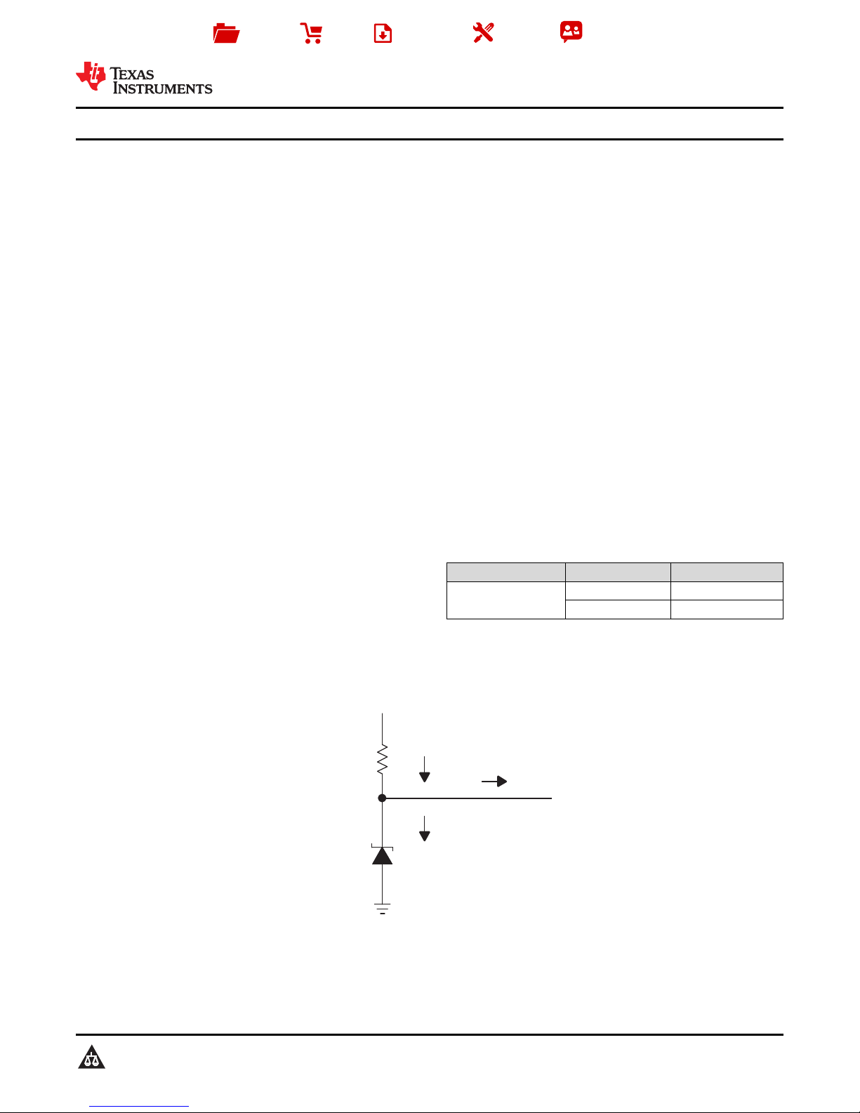
Simplified Schematic
1
An IMPORTANT NOTICE at the end of this data sheet addresses availability, warranty, changes, use in safety-critical applications,
intellectual property matters and other important disclaimers. PRODUCTION DATA.

LM4040A,LM4040B
LM4040C,LM4040D
SLOS456N –JANUARY 2005–REVISED OCTOBER 2017
www.ti.com
Table of Contents
1 Features.................................................................. 1
2 Applications ........................................................... 1
3 Description ............................................................. 1
4 Revision History..................................................... 2
5 Pin Configuration and Functions......................... 4
6 Specifications......................................................... 5
6.1 Absolute Maximum Ratings ...................................... 5
6.2 ESD Ratings.............................................................. 5
6.3 Recommended Operating Conditions....................... 5
6.4 Thermal Information.................................................. 5
6.5 LM4040A20I, LM4040B20I Electrical
Characteristics ........................................................... 6
6.6 LM4040C20I, LM4040D20I Electrical
Characteristics ........................................................... 7
6.7 LM4040C20Q, LM4040D20Q Electrical
Characteristics ........................................................... 8
6.8 LM4040A25I, LM4040B25I Electrical
Characteristics ........................................................... 9
6.9 LM4040C25I, LM4040D25I Electrical
Characteristics ......................................................... 10
6.10 LM4040C25Q, LM4040D25Q Electrical
Characteristics ......................................................... 11
6.11 LM4040A30I, LM4040B30I Electrical
Characteristics ......................................................... 12
6.12 LM4040C30I, LM4040D30I Electrical
Characteristics ......................................................... 13
6.13 LM4040C30Q, LM4040D30Q Electrical
Characteristics ......................................................... 14
6.14 LM4040A41I, LM4040B41I Electrical
Characteristics ......................................................... 15
6.15 LM4040C41I, LM4040D41I Electrical
Characteristics ......................................................... 16
6.16 LM4040A50I, LM4040B50I Electrical
Characteristics ......................................................... 17
6.17 LM4040C50I, LM4040D50I Electrical
Characteristics ......................................................... 18
6.18 LM4040C50Q, LM4040D50Q Electrical
Characteristics ......................................................... 19
6.19 LM4040A82I, LM4040B82I Electrical
Characteristics ......................................................... 20
6.20 LM4040C82I, LM4040D82I Electrical
Characteristics ......................................................... 21
6.21 LM4040A10I, LM4040B10I Electrical
Characteristics ......................................................... 22
6.22 LM4040C10I, LM4040D10I Electrical
Characteristics ......................................................... 23
6.23 Typical Characteristics.......................................... 24
7 Detailed Description............................................ 25
7.1 Overview ................................................................. 25
7.2 Functional Block Diagram....................................... 25
7.3 Feature Description................................................. 25
7.4 Device Functional Modes........................................ 25
8 Applications and Implementation ...................... 26
8.1 Application Information............................................ 26
8.2 Typical Applications ................................................ 26
9 Power Supply Recommendations...................... 29
10 Layout................................................................... 29
10.1 Layout Guidelines ................................................. 29
10.2 Layout Example .................................................... 29
11 Device and Documentation Support................. 30
11.1 Related Links ........................................................ 30
11.2 Trademarks........................................................... 30
11.3 Electrostatic Discharge Caution............................ 30
11.4 Glossary................................................................ 30
12 Mechanical, Packaging, and Orderable
Information........................................................... 30
4 Revision History
Changes from Revision M (January 2015) to Revision N Page
• Changed generic part number to include shorter list (LM4040A/B/C/D)................................................................................ 1
• Added Average temperature coefficient of reverse breakdown voltage footnote to all electrical tables................................ 6
• Changed Thermal hysteresis in electrical characteristics tables............................................................................................ 6
Changes from Revision L (January 2009) to Revision M Page
• Added Applications, Device Information table, Pin Functions table, ESD Ratings table, Thermal Information table,
Feature Description section, Device Functional Modes, Application and Implementation section, Power Supply
Recommendations section, Layout section, Device and Documentation Support section, and Mechanical,
Packaging, and Orderable Information section. ..................................................................................................................... 1
• Deleted Ordering Information table. ....................................................................................................................................... 1
2
Submit Documentation Feedback Copyright © 2005–2017, Texas Instruments Incorporated
Product Folder Links: LM4040A LM4040B LM4040C LM4040D

www.ti.com
LM4040A,LM4040B
LM4040C,LM4040D
SLOS456N –JANUARY 2005–REVISED OCTOBER 2017
(1)
ORDERABLE
PART NUMBER
T
A
–40°C to 85°C
–40°C to 85°C
–40°C to 85°C
–40°C to 125°C
Device Comparison Table
DEVICE
GRADE
A grade:
0.1% initial
accuracy
and
100 ppm/°C
temperature
coefficient
B grade:
0.2% initial
accuracy
and
100 ppm/°C
temperature
coefficient
C grade:
0.5% initial
accuracy
and
100 ppm/°C
temperature
coefficient
D grade:
1.0% initial
accuracy
and
150 ppm/°C
temperature
coefficient
C grade:
0.5% initial
accuracy
and
100 ppm/°C
temperature
coefficient
D grade:
1.0% initial
accuracy
and
150 ppm/°C
temperature
coefficient
V
KA
2.048 V LM4040A20I
2.5 V LM4040A25I
3 V LM4040A30I
4.096 V LM4040A41I
5 V LM4040A50I
8.192 V LM4040A82I
10 V LM4040A10I
2.048 V LM4040B20I
2.5 V LM4040B25I
3 V LM4040B30I
4.096 V LM4040B41I
5 V LM4040B50I
8.192 V LM4040B82I
10 V LM4040B10I
2.048 V LM4040C20I
2.5 V LM4040C25I
3 V LM4040C30I
4.096 V LM4040C41I
5 V LM4040C50I
8.192 V LM4040C82I
10 V LM4040C10I
2.048 V LM4040D20I
2.5 V LM4040D25I
3 V LM4040D30I
4.096 V LM4040D41I
5 V LM4040D50I
8.192 V LM4040D82I
10 V LM4040D10I
2.048 V LM4040C20Q
2.5 V LM4040C25Q
3 V LM4040C30Q
5 V LM4040C50Q
2.048 V LM4040D20Q
2.5 V LM4040D25Q
3 V LM4040D30Q
5 V LM4040D50Q
(1) For the most current package and ordering information, see the Package Option Addendum at the end of this document, or see the TI
web site at www.ti.com.
Product Folder Links: LM4040A LM4040B LM4040C LM4040D
Submit Documentation FeedbackCopyright © 2005–2017, Texas Instruments Incorporated
3

* Pin 3 is attached to substrate and must be
connected to ANODE or left open.
DBZ (SOT-23) PACKAGE
(TOP VIEW)
CATHODE
ANODE
DCK (SC-70) PACKAGE
(TOP VIEW)
ANODE
NC
CATHODE
NC
NC
1
2
3*
1
2
3
5
4
NC – No internal connection
LM4040A,LM4040B
LM4040C,LM4040D
SLOS456N –JANUARY 2005–REVISED OCTOBER 2017
5 Pin Configuration and Functions
www.ti.com
Pin Functions
PIN
NAME DBZ DCK
CATHODE 1 3 I/O Shunt Current/Voltage input
ANODE 2 1 O Common pin, normally connected to ground
NC — 2, 4, 5 I No Internal Connection
* 3 — I Substrate Connection
TYPE DESCRIPTION
4
Submit Documentation Feedback Copyright © 2005–2017, Texas Instruments Incorporated
Product Folder Links: LM4040A LM4040B LM4040C LM4040D
LM4040A,LM4040B
LM4040C,LM4040D
www.ti.com
SLOS456N –JANUARY 2005–REVISED OCTOBER 2017
6 Specifications
6.1 Absolute Maximum Ratings
over free-air temperature range (unless otherwise noted)
I
Z
T
J
T
stg
(1) Stresses beyond those listed under Absolute Maximum Ratings may cause permanent damage to the device. These are stress ratings
Continuous cathode current –10 25 mA
Operating virtual junction temperature 150 °C
Storage temperature range –65 150 °C
only, and functional operation of the device at these or any other conditions beyond those indicated under Recommended Operating
Conditionsis not implied. Exposure to absolute-maximum-rated conditions for extended periods may affect device reliability.
6.2 ESD Ratings
Human body model (HBM), per ANSI/ESDA/JEDEC JS-001, all pins
V
(ESD)
Electrostatic discharge
Charged device model (CDM), per JEDEC specification JESD22-C101,
(2)
all pins
(1) JEDEC document JEP155 states that 500-V HBM allows safe manufacturing with a standard ESD control process.
(2) JEDEC document JEP157 states that 250-V CDM allows safe manufacturing with a standard ESD control process.
6.3 Recommended Operating Conditions
I
Cathode current
Z
TAFree-air temperature
(1) See parametric tables
(1)
MIN MAX UNIT
VALUE UNIT
(1)
±2000
±1000
MIN MAX UNIT
(1)
LM4040xxxI –40 85
LM4040xxxQ –40 125
V
15 mA
°C
6.4 Thermal Information
LM4040
THERMAL METRIC
R
θJA
Junction-to-ambient thermal resistance 206 252 °C/W
(1) For more information about traditional and new thermal metrics, see the Semiconductor and IC Package Thermal Metrics application
report.
(1)
UNITDBZ DCK
3 PINS 5 PINS
Product Folder Links: LM4040A LM4040B LM4040C LM4040D
Submit Documentation FeedbackCopyright © 2005–2017, Texas Instruments Incorporated
5

DV
Z
DI
Z
LM4040A,LM4040B
LM4040C,LM4040D
SLOS456N –JANUARY 2005–REVISED OCTOBER 2017
www.ti.com
6.5 LM4040A20I, LM4040B20I Electrical Characteristics
at industrial temperature range, full-range TA= –40°C to 85°C (unless otherwise noted)
LM4040A20I LM4040B20I
MIN TYP MAX MIN TYP MAX
120 120 ppm
UNIT
mV
μA
ppm/°CIZ= 1 mA
mV
RMS
V
Z
ΔV
I
Z,min
PARAMETER TEST CONDITIONS T
Reverse breakdown voltage IZ= 100 μA 25°C 2.048 2.048 V
Reverse breakdown voltage
Z
tolerance
IZ= 100 μA
Minimum cathode current
A
25°C –2 2 –4.1 4.1
Full range –15 15 –17 17
25°C 45 75 45 75
Full range 80 80
IZ= 10 mA 25°C ±20 ±20
α
of reverse breakdown voltage
VZ
(1)
Average temperature coefficient
25°C ±15 ±15
Full range ±100 ±100
IZ= 100 μA 25°C ±15 ±15
25°C 0.3 0.8 0.3 0.8
Full range 1 1
25°C 2.5 6 2.5 6
Full range 8 8
25°C 0.3 0.8 0.3 0.8 Ω
25°C 35 35 μV
Z
e
V
Reverse breakdown voltage
change with cathode current
change
Reverse dynamic impedance
Z
Wideband noise
N
Long-term stability of reverse
breakdown voltage
Thermal hysteresis
HYST
I
< IZ< 1 mA
Z,min
1 mA < IZ< 15 mA
IZ= 1 mA, f = 120 Hz,
IAC= 0.1 I
Z
IZ= 100 μA,
10 Hz ≤ f ≤ 10 kHz
t = 1000 h,
TA= 25°C ± 0.1°C,
IZ= 100 μA
(2)
ΔTA= –40°C to 125°C 0.08% 0.08% —
(1) The overtemperature limit for Reverse Breakdown Voltage Tolerance is defined as the room temperature Reverse Breakdown Voltage
Tolerance ±[(ΔVR/ΔT)(maxΔT)(VR)]. Where, ΔVR/ΔT is the VRtemperature coefficient, maxΔT is the maximum difference in temperature
from the reference point of 25°C to T
different grades in the industrial temperature range where maxΔT = 65°C is shown below:
MIN
or T
, and VRis the reverse breakdown voltage. The total overtemperature tolerance for the
MAX
A-grade: ±0.75% = ±0.1% ±100 ppm/°C × 65°C
B-grade: ±0.85% = ±0.2% ±100 ppm/°C × 65°C
C-grade: ±1.15% = ±0.5% ±100 ppm/°C × 65°C
D-grade: ±1.98% = ±1.0% ±150 ppm/°C × 65°C
The total overtemperature tolerance for the different grades in the extended temperature range where max ΔT = 100 °C is shown below:
C-grade: ±1.5% = ±0.5% ±100 ppm/°C × 100°C
D-grade: ±2.5% = ±1.0% ±150 ppm/°C × 100°C
Therefore, as an example, the A-grade 2.5-V LM4040 has an overtemperature Reverse Breakdown Voltage tolerance of ±2.5 V × 0.75%
= ±19 mV.
(2) Thermal hysteresis is defined as the difference in voltage measured at 25°C after cycling to temperature –40°C and the 25°C
measurement after cycling to temperature 125°C.
6
Submit Documentation Feedback Copyright © 2005–2017, Texas Instruments Incorporated
Product Folder Links: LM4040A LM4040B LM4040C LM4040D

DV
Z
DI
Z
LM4040A,LM4040B
LM4040C,LM4040D
www.ti.com
SLOS456N –JANUARY 2005–REVISED OCTOBER 2017
6.6 LM4040C20I, LM4040D20I Electrical Characteristics
at industrial temperature range, full-range TA= –40°C to 85°C (unless otherwise noted)
LM4040C20I LM4040D20I
MIN TYP MAX MIN TYP MAX
120 120 ppm
UNIT
mV
μA
ppm/°CIZ= 1 mA
mV
RMS
V
Z
ΔV
I
Z,min
PARAMETER TEST CONDITIONS T
Reverse breakdown voltage IZ= 100 μA 25°C 2.048 2.048 V
Reverse breakdown voltage
Z
tolerance
IZ= 100 μA
Minimum cathode current
A
25°C –10 10 –20 20
Full range –23 23 –40 40
25°C 45 75 45 75
Full range 80 80
IZ= 10 mA 25°C ±20 ±20
α
of reverse breakdown voltage
VZ
(1)
Average temperature coefficient
25°C ±15 ±15
Full range ±100 ±150
IZ= 100 μA 25°C ±15 ±15
25°C 0.3 0.8 0.3 1
Full range 1 1.2
25°C 2.5 6 2.5 8
Full range 8 10
25°C 0.3 0.9 0.3 1.1 Ω
25°C 35 35 μV
Z
e
V
Reverse breakdown voltage
change with cathode current
change
Reverse dynamic impedance
Z
Wideband noise
N
Long-term stability of reverse
breakdown voltage
Thermal hysteresis
HYST
I
< IZ< 1 mA
Z,min
1 mA < IZ< 15 mA
IZ= 1 mA, f = 120 Hz,
IAC= 0.1 I
Z
IZ= 100 μA,
10 Hz ≤ f ≤ 10 kHz
t = 1000 h,
TA= 25°C ± 0.1°C,
IZ= 100 μA
(2)
ΔTA= –40°C to 125°C 0.08% 0.08% —
(1) The overtemperature limit for Reverse Breakdown Voltage Tolerance is defined as the room temperature Reverse Breakdown Voltage
Tolerance ±[(ΔVR/ΔT)(maxΔT)(VR)]. Where, ΔVR/ΔT is the VRtemperature coefficient, maxΔT is the maximum difference in temperature
from the reference point of 25°C to T
different grades in the industrial temperature range where maxΔT = 65°C is shown below:
MIN
or T
, and VRis the reverse breakdown voltage. The total overtemperature tolerance for the
MAX
A-grade: ±0.75% = ±0.1% ±100 ppm/°C × 65°C
B-grade: ±0.85% = ±0.2% ±100 ppm/°C × 65°C
C-grade: ±1.15% = ±0.5% ±100 ppm/°C × 65°C
D-grade: ±1.98% = ±1.0% ±150 ppm/°C × 65°C
The total overtemperature tolerance for the different grades in the extended temperature range where max ΔT = 100 °C is shown below:
C-grade: ±1.5% = ±0.5% ±100 ppm/°C × 100°C
D-grade: ±2.5% = ±1.0% ±150 ppm/°C × 100°C
Therefore, as an example, the A-grade 2.5-V LM4040 has an overtemperature Reverse Breakdown Voltage tolerance of ±2.5 V × 0.75%
= ±19 mV.
(2) Thermal hysteresis is defined as the difference in voltage measured at 25°C after cycling to temperature –40°C and the 25°C
measurement after cycling to temperature 125°C.
Product Folder Links: LM4040A LM4040B LM4040C LM4040D
Submit Documentation FeedbackCopyright © 2005–2017, Texas Instruments Incorporated
7
DV
Z
DI
Z
LM4040A,LM4040B
LM4040C,LM4040D
SLOS456N –JANUARY 2005–REVISED OCTOBER 2017
www.ti.com
6.7 LM4040C20Q, LM4040D20Q Electrical Characteristics
at extended temperature range, full-range TA= –40°C to 125°C (unless otherwise noted)
LM4040C20Q LM4040D20Q
MIN TYP MAX MIN TYP MAX
120 120 ppm
UNIT
mV
μA
ppm/°CIZ= 1 mA
mV
RMS
V
Z
ΔV
I
Z,min
PARAMETER TEST CONDITIONS T
Reverse breakdown voltage IZ= 100 μA 25°C 2.048 2.048 V
Reverse breakdown voltage
Z
tolerance
IZ= 100 μA
Minimum cathode current
A
25°C –10 10 –20 20
Full range –30 30 –50 50
25°C 45 75 45 75
Full range 80 80
IZ= 10 mA 25°C ±20 ±20
α
of reverse breakdown voltage
VZ
(1)
Average temperature coefficient
25°C ±15 ±15
Full range ±100 ±150
IZ= 100 μA 25°C ±15 ±15
25°C 0.3 0.8 0.3 1
Full range 1 1.2
25°C 2.5 6 2.5 8
Full range 8 10
25°C 0.3 0.9 0.3 1.1 Ω
25°C 35 35 μV
Z
e
V
Reverse breakdown voltage
change with cathode current
change
Reverse dynamic impedance
Z
Wideband noise
N
Long-term stability of reverse
breakdown voltage
Thermal hysteresis
HYST
I
< IZ< 1 mA
Z,min
1 mA < IZ< 15 mA
IZ= 1 mA, f = 120 Hz,
IAC= 0.1 I
Z
IZ= 100 μA,
10 Hz ≤ f ≤ 10 kHz
t = 1000 h,
TA= 25°C ± 0.1°C,
IZ= 100 μA
(2)
ΔTA= –40°C to 125°C 0.08% 0.08% —
(1) The overtemperature limit for Reverse Breakdown Voltage Tolerance is defined as the room temperature Reverse Breakdown Voltage
Tolerance ±[(ΔVR/ΔT)(maxΔT)(VR)]. Where, ΔVR/ΔT is the VRtemperature coefficient, maxΔT is the maximum difference in temperature
from the reference point of 25°C to T
different grades in the industrial temperature range where maxΔT = 65°C is shown below:
MIN
or T
, and VRis the reverse breakdown voltage. The total overtemperature tolerance for the
MAX
A-grade: ±0.75% = ±0.1% ±100 ppm/°C × 65°C
B-grade: ±0.85% = ±0.2% ±100 ppm/°C × 65°C
C-grade: ±1.15% = ±0.5% ±100 ppm/°C × 65°C
D-grade: ±1.98% = ±1.0% ±150 ppm/°C × 65°C
The total overtemperature tolerance for the different grades in the extended temperature range where max ΔT = 100 °C is shown below:
C-grade: ±1.5% = ±0.5% ±100 ppm/°C × 100°C
D-grade: ±2.5% = ±1.0% ±150 ppm/°C × 100°C
Therefore, as an example, the A-grade 2.5-V LM4040 has an overtemperature Reverse Breakdown Voltage tolerance of ±2.5 V × 0.75%
= ±19 mV.
(2) Thermal hysteresis is defined as the difference in voltage measured at 25°C after cycling to temperature –40°C and the 25°C
measurement after cycling to temperature 125°C.
8
Submit Documentation Feedback Copyright © 2005–2017, Texas Instruments Incorporated
Product Folder Links: LM4040A LM4040B LM4040C LM4040D

DV
Z
DI
Z
LM4040A,LM4040B
LM4040C,LM4040D
www.ti.com
SLOS456N –JANUARY 2005–REVISED OCTOBER 2017
6.8 LM4040A25I, LM4040B25I Electrical Characteristics
at industrial temperature range, full-range TA= –40°C to 85°C (unless otherwise noted)
LM4040A25I LM4040B25I
MIN TYP MAX MIN TYP MAX
120 120 ppm
UNIT
mV
μA
ppm/°CIZ= 1 mA
mV
RMS
V
Z
ΔV
I
Z,min
PARAMETER TEST CONDITIONS T
Reverse breakdown voltage IZ= 100 μA 25°C 2.5 2.5 V
Reverse breakdown voltage
Z
tolerance
IZ= 100 μA
Minimum cathode current
A
25°C –2.5 2.5 –5 5
Full range –19 19 –21 21
25°C 45 75 45 75
Full range 80 80
IZ= 10 mA 25°C ±20 ±20
α
of reverse breakdown voltage
VZ
(1)
Average temperature coefficient
25°C ±15 ±15
Full range ±100 ±100
IZ= 100 μA 25°C ±15 ±15
25°C 0.3 0.8 0.3 0.8
Full range 1 1
25°C 2.5 6 2.5 6
Full range 8 8
25°C 0.3 0.8 0.3 0.8 Ω
25°C 35 35 μV
Z
e
V
Reverse breakdown voltage
change with cathode current
change
Reverse dynamic impedance
Z
Wideband noise
N
Long-term stability of reverse
breakdown voltage
Thermal hysteresis
HYST
I
< IZ< 1 mA
Z,min
1 mA < IZ< 15 mA
IZ= 1 mA, f = 120 Hz,
IAC= 0.1 I
Z
IZ= 100 μA,
10 Hz ≤ f ≤ 10 kHz
t = 1000 h,
TA= 25°C ± 0.1°C,
IZ= 100 μA
(2)
ΔTA= –40°C to 125°C 0.08% 0.08% —
(1) The overtemperature limit for Reverse Breakdown Voltage Tolerance is defined as the room temperature Reverse Breakdown Voltage
Tolerance ±[(ΔVR/ΔT)(maxΔT)(VR)]. Where, ΔVR/ΔT is the VRtemperature coefficient, maxΔT is the maximum difference in temperature
from the reference point of 25°C to T
different grades in the industrial temperature range where maxΔT = 65°C is shown below:
MIN
or T
, and VRis the reverse breakdown voltage. The total overtemperature tolerance for the
MAX
A-grade: ±0.75% = ±0.1% ±100 ppm/°C × 65°C
B-grade: ±0.85% = ±0.2% ±100 ppm/°C × 65°C
C-grade: ±1.15% = ±0.5% ±100 ppm/°C × 65°C
D-grade: ±1.98% = ±1.0% ±150 ppm/°C × 65°C
The total overtemperature tolerance for the different grades in the extended temperature range where max ΔT = 100 °C is shown below:
C-grade: ±1.5% = ±0.5% ±100 ppm/°C × 100°C
D-grade: ±2.5% = ±1.0% ±150 ppm/°C × 100°C
Therefore, as an example, the A-grade 2.5-V LM4040 has an overtemperature Reverse Breakdown Voltage tolerance of ±2.5 V × 0.75%
= ±19 mV.
(2) Thermal hysteresis is defined as the difference in voltage measured at 25°C after cycling to temperature –40°C and the 25°C
measurement after cycling to temperature 125°C.
Product Folder Links: LM4040A LM4040B LM4040C LM4040D
Submit Documentation FeedbackCopyright © 2005–2017, Texas Instruments Incorporated
9

DV
Z
DI
Z
LM4040A,LM4040B
LM4040C,LM4040D
SLOS456N –JANUARY 2005–REVISED OCTOBER 2017
www.ti.com
6.9 LM4040C25I, LM4040D25I Electrical Characteristics
at industrial temperature range, full-range TA= –40°C to 85°C (unless otherwise noted)
LM4040C25I LM4040D25I
MIN TYP MAX MIN TYP MAX
120 120 ppm
UNIT
mV
μA
ppm/°CIZ= 1 mA
mV
RMS
V
Z
ΔV
I
Z,min
PARAMETER TEST CONDITIONS T
Reverse breakdown voltage IZ= 100 μA 25°C 2.5 2.5 V
Reverse breakdown voltage
Z
tolerance
IZ= 100 μA
Minimum cathode current
A
25°C –12 12 –25 25
Full range –29 29 –49 49
25°C 45 75 45 75
Full range 80 80
IZ= 10 mA 25°C ±20 ±20
α
of reverse breakdown voltage
VZ
(1)
Average temperature coefficient
25°C ±15 ±15
Full range ±100 ±150
IZ= 100 μA 25°C ±15 ±15
25°C 0.3 0.8 0.3 1
Full range 1 1.2
25°C 2.5 6 2.5 8
Full range 8 10
25°C 0.3 0.9 0.3 1.1 Ω
25°C 35 35 μV
Z
e
V
Reverse breakdown voltage
change with cathode current
change
Reverse dynamic impedance
Z
Wideband noise
N
Long-term stability of reverse
breakdown voltage
Thermal hysteresis
HYST
I
< IZ< 1 mA
Z,min
1 mA < IZ< 15 mA
IZ= 1 mA, f = 120 Hz,
IAC= 0.1 I
Z
IZ= 100 μA,
10 Hz ≤ f ≤ 10 kHz
t = 1000 h,
TA= 25°C ± 0.1°C,
IZ= 100 μA
(2)
ΔTA= –40°C to 125°C 0.08% 0.08% —
(1) The overtemperature limit for Reverse Breakdown Voltage Tolerance is defined as the room temperature Reverse Breakdown Voltage
Tolerance ±[(ΔVR/ΔT)(maxΔT)(VR)]. Where, ΔVR/ΔT is the VRtemperature coefficient, maxΔT is the maximum difference in temperature
from the reference point of 25°C to T
different grades in the industrial temperature range where maxΔT = 65°C is shown below:
MIN
or T
, and VRis the reverse breakdown voltage. The total overtemperature tolerance for the
MAX
A-grade: ±0.75% = ±0.1% ±100 ppm/°C × 65°C
B-grade: ±0.85% = ±0.2% ±100 ppm/°C × 65°C
C-grade: ±1.15% = ±0.5% ±100 ppm/°C × 65°C
D-grade: ±1.98% = ±1.0% ±150 ppm/°C × 65°C
The total overtemperature tolerance for the different grades in the extended temperature range where max ΔT = 100 °C is shown below:
C-grade: ±1.5% = ±0.5% ±100 ppm/°C × 100°C
D-grade: ±2.5% = ±1.0% ±150 ppm/°C × 100°C
Therefore, as an example, the A-grade 2.5-V LM4040 has an overtemperature Reverse Breakdown Voltage tolerance of ±2.5 V × 0.75%
= ±19 mV.
(2) Thermal hysteresis is defined as the difference in voltage measured at 25°C after cycling to temperature –40°C and the 25°C
measurement after cycling to temperature 125°C.
10
Submit Documentation Feedback Copyright © 2005–2017, Texas Instruments Incorporated
Product Folder Links: LM4040A LM4040B LM4040C LM4040D

DV
Z
DI
Z
LM4040A,LM4040B
LM4040C,LM4040D
www.ti.com
SLOS456N –JANUARY 2005–REVISED OCTOBER 2017
6.10 LM4040C25Q, LM4040D25Q Electrical Characteristics
at extended temperature range, full-range TA= –40°C to 125°C (unless otherwise noted)
LM4040C25Q LM4040D25Q
MIN TYP MAX MIN TYP MAX
120 120 ppm
UNIT
mV
μA
ppm/°CIZ= 1 mA
mV
RMS
V
Z
ΔV
I
Z,min
PARAMETER TEST CONDITIONS T
Reverse breakdown voltage IZ= 100 μA 25°C 2.5 2.5 V
Reverse breakdown voltage
Z
tolerance
IZ= 100 μA
Minimum cathode current
A
25°C –12 12 –25 25
Full range –38 38 –63 63
25°C 45 75 45 75
Full range 80 80
IZ= 10 mA 25°C ±20 ±20
α
of reverse breakdown voltage
VZ
(1)
Average temperature coefficient
25°C ±15 ±15
Full range ±100 ±150
IZ= 100 μA 25°C ±15 ±15
25°C 0.3 0.8 0.3 1
Full range 1 1.2
25°C 2.5 6 2.5 8
Full range 8 10
25°C 0.3 0.9 0.3 1.1 Ω
25°C 35 35 μV
Z
e
V
Reverse breakdown voltage
change with cathode current
change
Reverse dynamic impedance
Z
Wideband noise
N
Long-term stability of reverse
breakdown voltage
Thermal hysteresis
HYST
I
< IZ< 1 mA
Z,min
1 mA < IZ< 15 mA
IZ= 1 mA, f = 120 Hz,
IAC= 0.1 I
Z
IZ= 100 μA,
10 Hz ≤ f ≤ 10 kHz
t = 1000 h,
TA= 25°C ± 0.1°C,
IZ= 100 μA
(2)
ΔTA= –40°C to 125°C 0.08% 0.08% —
(1) The overtemperature limit for Reverse Breakdown Voltage Tolerance is defined as the room temperature Reverse Breakdown Voltage
Tolerance ±[(ΔVR/ΔT)(maxΔT)(VR)]. Where, ΔVR/ΔT is the VRtemperature coefficient, maxΔT is the maximum difference in temperature
from the reference point of 25°C to T
different grades in the industrial temperature range where maxΔT = 65°C is shown below:
MIN
or T
, and VRis the reverse breakdown voltage. The total overtemperature tolerance for the
MAX
A-grade: ±0.75% = ±0.1% ±100 ppm/°C × 65°C
B-grade: ±0.85% = ±0.2% ±100 ppm/°C × 65°C
C-grade: ±1.15% = ±0.5% ±100 ppm/°C × 65°C
D-grade: ±1.98% = ±1.0% ±150 ppm/°C × 65°C
The total overtemperature tolerance for the different grades in the extended temperature range where max ΔT = 100 °C is shown below:
C-grade: ±1.5% = ±0.5% ±100 ppm/°C × 100°C
D-grade: ±2.5% = ±1.0% ±150 ppm/°C × 100°C
Therefore, as an example, the A-grade 2.5-V LM4040 has an overtemperature Reverse Breakdown Voltage tolerance of ±2.5 V × 0.75%
= ±19 mV.
(2) Thermal hysteresis is defined as the difference in voltage measured at 25°C after cycling to temperature –40°C and the 25°C
measurement after cycling to temperature 125°C.
Product Folder Links: LM4040A LM4040B LM4040C LM4040D
Submit Documentation FeedbackCopyright © 2005–2017, Texas Instruments Incorporated
11

DV
Z
DI
Z
LM4040A,LM4040B
LM4040C,LM4040D
SLOS456N –JANUARY 2005–REVISED OCTOBER 2017
www.ti.com
6.11 LM4040A30I, LM4040B30I Electrical Characteristics
at industrial temperature range, full-range TA= –40°C to 85°C (unless otherwise noted)
LM4040A30I LM4040B30I
MIN TYP MAX MIN TYP MAX
120 120 ppm
UNIT
mV
μA
ppm/°CIZ= 1 mA
mV
RMS
V
Z
ΔV
I
Z,min
PARAMETER TEST CONDITIONS T
Reverse breakdown voltage IZ= 100 μA 25°C 3 3 V
Reverse breakdown voltage
Z
tolerance
IZ= 100 μA
Minimum cathode current
A
25°C –3 3 –6 6
Full range –22 22 –26 26
25°C 47 77 47 77
Full range 82 82
IZ= 10 mA 25°C ±20 ±20
α
of reverse breakdown voltage
VZ
(1)
Average temperature coefficient
25°C ±15 ±15
Full range ±100 ±100
IZ= 100 μA 25°C ±15 ±15
25°C 0.6 0.8 0.6 0.8
Full range 1.1 1.1
25°C 2.7 6 2.7 6
Full range 9 9
25°C 0.4 0.9 0.4 0.9 Ω
25°C 35 35 μV
Z
e
V
Reverse breakdown voltage
change with cathode current
change
Reverse dynamic impedance
Z
Wideband noise
N
Long-term stability of reverse
breakdown voltage
Thermal hysteresis
HYST
I
< IZ< 1 mA
Z,min
1 mA < IZ< 15 mA
IZ= 1 mA, f = 120 Hz,
IAC= 0.1 I
Z
IZ= 100 μA,
10 Hz ≤ f ≤ 10 kHz
t = 1000 h,
TA= 25°C ± 0.1°C,
IZ= 100 μA
(2)
ΔTA= –40°C to 125°C 0.08% 0.08% —
(1) The overtemperature limit for Reverse Breakdown Voltage Tolerance is defined as the room temperature Reverse Breakdown Voltage
Tolerance ±[(ΔVR/ΔT)(maxΔT)(VR)]. Where, ΔVR/ΔT is the VRtemperature coefficient, maxΔT is the maximum difference in temperature
from the reference point of 25°C to T
different grades in the industrial temperature range where maxΔT = 65°C is shown below:
MIN
or T
, and VRis the reverse breakdown voltage. The total overtemperature tolerance for the
MAX
A-grade: ±0.75% = ±0.1% ±100 ppm/°C × 65°C
B-grade: ±0.85% = ±0.2% ±100 ppm/°C × 65°C
C-grade: ±1.15% = ±0.5% ±100 ppm/°C × 65°C
D-grade: ±1.98% = ±1.0% ±150 ppm/°C × 65°C
The total overtemperature tolerance for the different grades in the extended temperature range where max ΔT = 100 °C is shown below:
C-grade: ±1.5% = ±0.5% ±100 ppm/°C × 100°C
D-grade: ±2.5% = ±1.0% ±150 ppm/°C × 100°C
Therefore, as an example, the A-grade 2.5-V LM4040 has an overtemperature Reverse Breakdown Voltage tolerance of ±2.5 V × 0.75%
= ±19 mV.
(2) Thermal hysteresis is defined as the difference in voltage measured at 25°C after cycling to temperature –40°C and the 25°C
measurement after cycling to temperature 125°C.
12
Submit Documentation Feedback Copyright © 2005–2017, Texas Instruments Incorporated
Product Folder Links: LM4040A LM4040B LM4040C LM4040D
DV
Z
DI
Z
LM4040A,LM4040B
LM4040C,LM4040D
www.ti.com
SLOS456N –JANUARY 2005–REVISED OCTOBER 2017
6.12 LM4040C30I, LM4040D30I Electrical Characteristics
at industrial temperature range, full-range TA= –40°C to 85°C (unless otherwise noted)
LM4040C30I LM4040D30I
MIN TYP MAX MIN TYP MAX
120 120 ppm
UNIT
mV
μA
ppm/°CIZ= 1 mA
mV
RMS
V
Z
ΔV
I
Z,min
PARAMETER TEST CONDITIONS T
Reverse breakdown voltage IZ= 100 μA 25°C 3 3 V
Reverse breakdown voltage
Z
tolerance
IZ= 100 μA
Minimum cathode current
A
25°C –15 15 –30 30
Full range –34 34 –59 59
25°C 45 77 45 77
Full range 82 82
IZ= 10 mA 25°C ±20 ±20
α
of reverse breakdown voltage
VZ
(1)
Average temperature coefficient
25°C ±15 ±15
Full range ±100 ±150
IZ= 100 μA 25°C ±15 ±15
25°C 0.4 0.8 1.4 1
Full range 1.1 1.3
25°C 2.7 6 2.7 8
Full range 9 11
25°C 0.4 0.9 0.4 1.2 Ω
25°C 35 35 μV
Z
e
V
Reverse breakdown voltage
change with cathode current
change
Reverse dynamic impedance
Z
Wideband noise
N
Long-term stability of reverse
breakdown voltage
Thermal hysteresis
HYST
I
< IZ< 1 mA
Z,min
1 mA < IZ< 15 mA
IZ= 1 mA, f = 120 Hz,
IAC= 0.1 I
Z
IZ= 100 μA,
10 Hz ≤ f ≤ 10 kHz
t = 1000 h,
TA= 25°C ± 0.1°C,
IZ= 100 μA
(2)
ΔTA= –40°C to 125°C 0.08% 0.08% —
(1) The overtemperature limit for Reverse Breakdown Voltage Tolerance is defined as the room temperature Reverse Breakdown Voltage
Tolerance ±[(ΔVR/ΔT)(maxΔT)(VR)]. Where, ΔVR/ΔT is the VRtemperature coefficient, maxΔT is the maximum difference in temperature
from the reference point of 25°C to T
different grades in the industrial temperature range where maxΔT = 65°C is shown below:
MIN
or T
, and VRis the reverse breakdown voltage. The total overtemperature tolerance for the
MAX
A-grade: ±0.75% = ±0.1% ±100 ppm/°C × 65°C
B-grade: ±0.85% = ±0.2% ±100 ppm/°C × 65°C
C-grade: ±1.15% = ±0.5% ±100 ppm/°C × 65°C
D-grade: ±1.98% = ±1.0% ±150 ppm/°C × 65°C
The total overtemperature tolerance for the different grades in the extended temperature range where max ΔT = 100 °C is shown below:
C-grade: ±1.5% = ±0.5% ±100 ppm/°C × 100°C
D-grade: ±2.5% = ±1.0% ±150 ppm/°C × 100°C
Therefore, as an example, the A-grade 2.5-V LM4040 has an overtemperature Reverse Breakdown Voltage tolerance of ±2.5 V × 0.75%
= ±19 mV.
(2) Thermal hysteresis is defined as the difference in voltage measured at 25°C after cycling to temperature –40°C and the 25°C
measurement after cycling to temperature 125°C.
Product Folder Links: LM4040A LM4040B LM4040C LM4040D
Submit Documentation FeedbackCopyright © 2005–2017, Texas Instruments Incorporated
13

DV
Z
DI
Z
LM4040A,LM4040B
LM4040C,LM4040D
SLOS456N –JANUARY 2005–REVISED OCTOBER 2017
www.ti.com
6.13 LM4040C30Q, LM4040D30Q Electrical Characteristics
at extended temperature range, full-range TA= –40°C to 125°C (unless otherwise noted)
LM4040C30Q LM4040D30Q
MIN TYP MAX MIN TYP MAX
120 120 ppm
UNIT
mV
μA
ppm/°CIZ= 1 mA
mV
RMS
V
Z
ΔV
I
Z,min
PARAMETER TEST CONDITIONS T
Reverse breakdown voltage IZ= 100 μA 25°C 3 3 V
Reverse breakdown voltage
Z
tolerance
IZ= 100 μA
Minimum cathode current
A
25°C –15 15 –30 30
Full range –45 45 –75 75
25°C 47 77 47 77
Full range 82 82
IZ= 10 mA 25°C ±20 ±20
α
of reverse breakdown voltage
VZ
(1)
Average temperature coefficient
25°C ±15 ±15
Full range ±100 ±150
IZ= 100 μA 25°C ±15 ±15
25°C 0.4 0.8 0.4 1.1
Full range 1.1 1.3
25°C 2.7 6 2.7 8
Full range 9 11
25°C 0.4 0.9 0.4 1.2 Ω
25°C 35 35 μV
Z
e
V
Reverse breakdown voltage
change with cathode current
change
Reverse dynamic impedance
Z
Wideband noise
N
Long-term stability of reverse
breakdown voltage
Thermal hysteresis
HYST
I
< IZ< 1 mA
Z,min
1 mA < IZ< 15 mA
IZ= 1 mA, f = 120 Hz,
IAC= 0.1 I
Z
IZ= 100 μA,
10 Hz ≤ f ≤ 10 kHz
t = 1000 h,
TA= 25°C ± 0.1°C,
IZ= 100 μA
(2)
ΔTA= –40°C to 125°C 0.08% 0.08% —
(1) The overtemperature limit for Reverse Breakdown Voltage Tolerance is defined as the room temperature Reverse Breakdown Voltage
Tolerance ±[(ΔVR/ΔT)(maxΔT)(VR)]. Where, ΔVR/ΔT is the VRtemperature coefficient, maxΔT is the maximum difference in temperature
from the reference point of 25°C to T
different grades in the industrial temperature range where maxΔT = 65°C is shown below:
MIN
or T
, and VRis the reverse breakdown voltage. The total overtemperature tolerance for the
MAX
A-grade: ±0.75% = ±0.1% ±100 ppm/°C × 65°C
B-grade: ±0.85% = ±0.2% ±100 ppm/°C × 65°C
C-grade: ±1.15% = ±0.5% ±100 ppm/°C × 65°C
D-grade: ±1.98% = ±1.0% ±150 ppm/°C × 65°C
The total overtemperature tolerance for the different grades in the extended temperature range where max ΔT = 100 °C is shown below:
C-grade: ±1.5% = ±0.5% ±100 ppm/°C × 100°C
D-grade: ±2.5% = ±1.0% ±150 ppm/°C × 100°C
Therefore, as an example, the A-grade 2.5-V LM4040 has an overtemperature Reverse Breakdown Voltage tolerance of ±2.5 V × 0.75%
= ±19 mV.
(2) Thermal hysteresis is defined as the difference in voltage measured at 25°C after cycling to temperature –40°C and the 25°C
measurement after cycling to temperature 125°C.
14
Submit Documentation Feedback Copyright © 2005–2017, Texas Instruments Incorporated
Product Folder Links: LM4040A LM4040B LM4040C LM4040D

DV
Z
DI
Z
LM4040A,LM4040B
LM4040C,LM4040D
www.ti.com
SLOS456N –JANUARY 2005–REVISED OCTOBER 2017
6.14 LM4040A41I, LM4040B41I Electrical Characteristics
at industrial temperature range, full-range TA= –40°C to 85°C (unless otherwise noted)
LM4040A41I LM4040B41I
MIN TYP MAX MIN TYP MAX
120 120 ppm
UNIT
mV
μA
ppm/°CIZ= 1 mA
mV
RMS
V
Z
ΔV
I
Z,min
PARAMETER TEST CONDITIONS T
Reverse breakdown voltage IZ= 100 μA 25°C 4.096 4.096 V
Reverse breakdown voltage
Z
tolerance
IZ= 100 μA
Minimum cathode current
A
25°C –4.1 4.1 –8.2 8.2
Full range –31 31 –35 35
25°C 50 83 50 83
Full range 88 88
IZ= 10 mA 25°C ±30 ±30
α
of reverse breakdown voltage
VZ
(1)
Average temperature coefficient
25°C ±20 ±20
Full range ±100 ±100
IZ= 100 μA 25°C ±20 ±20
25°C 0.5 0.9 0.5 0.9
Full range 1.2 1.2
25°C 3 7 3 7
Full range 10 10
25°C 0.5 1 0.5 1 Ω
25°C 80 80 μV
Z
e
V
Reverse breakdown voltage
change with cathode current
change
Reverse dynamic impedance
Z
Wideband noise
N
Long-term stability of reverse
breakdown voltage
Thermal hysteresis
HYST
I
< IZ< 1 mA
Z,min
1 mA < IZ< 15 mA
IZ= 1 mA, f = 120 Hz,
IAC= 0.1 I
Z
IZ= 100 μA,
10 Hz ≤ f ≤ 10 kHz
t = 1000 h,
TA= 25°C ± 0.1°C,
IZ= 100 μA
(2)
ΔTA= –40°C to 125°C 0.08% 0.08% —
(1) The overtemperature limit for Reverse Breakdown Voltage Tolerance is defined as the room temperature Reverse Breakdown Voltage
Tolerance ±[(ΔVR/ΔT)(maxΔT)(VR)]. Where, ΔVR/ΔT is the VRtemperature coefficient, maxΔT is the maximum difference in temperature
from the reference point of 25°C to T
different grades in the industrial temperature range where maxΔT = 65°C is shown below:
MIN
or T
, and VRis the reverse breakdown voltage. The total overtemperature tolerance for the
MAX
A-grade: ±0.75% = ±0.1% ±100 ppm/°C × 65°C
B-grade: ±0.85% = ±0.2% ±100 ppm/°C × 65°C
C-grade: ±1.15% = ±0.5% ±100 ppm/°C × 65°C
D-grade: ±1.98% = ±1.0% ±150 ppm/°C × 65°C
The total overtemperature tolerance for the different grades in the extended temperature range where max ΔT = 100 °C is shown below:
C-grade: ±1.5% = ±0.5% ±100 ppm/°C × 100°C
D-grade: ±2.5% = ±1.0% ±150 ppm/°C × 100°C
Therefore, as an example, the A-grade 2.5-V LM4040 has an overtemperature Reverse Breakdown Voltage tolerance of ±2.5 V × 0.75%
= ±19 mV.
(2) Thermal hysteresis is defined as the difference in voltage measured at 25°C after cycling to temperature –40°C and the 25°C
measurement after cycling to temperature 125°C.
Product Folder Links: LM4040A LM4040B LM4040C LM4040D
Submit Documentation FeedbackCopyright © 2005–2017, Texas Instruments Incorporated
15

DV
Z
DI
Z
LM4040A,LM4040B
LM4040C,LM4040D
SLOS456N –JANUARY 2005–REVISED OCTOBER 2017
www.ti.com
6.15 LM4040C41I, LM4040D41I Electrical Characteristics
at industrial temperature range, full-range TA= –40°C to 85°C (unless otherwise noted)
LM4040C41I LM4040D41I
MIN TYP MAX MIN TYP MAX
120 120 ppm
UNIT
mV
μA
ppm/°CIZ= 1 mA
mV
RMS
V
Z
ΔV
I
Z,min
PARAMETER TEST CONDITIONS T
Reverse breakdown voltage IZ= 100 μA 25°C 4.096 4.096 V
Reverse breakdown voltage
Z
tolerance
IZ= 100 μA
Minimum cathode current
A
25°C –20 20 –41 41
Full range –47 47 –81 81
25°C 50 83 50 83
Full range 88 88
IZ= 10 mA 25°C ±30 ±30
α
of reverse breakdown voltage
VZ
(1)
Average temperature coefficient
25°C ±20 ±20
Full range ±100 ±150
IZ= 100 μA 25°C ±20 ±20
25°C 0.5 0.9 0.5 1.2
Full range 1.2 1.5
25°C 3 7 3 9
Full range 10 13
25°C 0.5 1 0.5 1.3 Ω
25°C 80 80 μV
Z
e
V
Reverse breakdown voltage
change with cathode current
change
Reverse dynamic impedance
Z
Wideband noise
N
Long-term stability of reverse
breakdown voltage
Thermal hysteresis
HYST
I
< IZ< 1 mA
Z,min
1 mA < IZ< 15 mA
IZ= 1 mA, f = 120 Hz,
IAC= 0.1 I
Z
IZ= 100 μA,
10 Hz ≤ f ≤ 10 kHz
t = 1000 h,
TA= 25°C ± 0.1°C,
IZ= 100 μA
(2)
ΔTA= –40°C to 125°C 0.08% 0.08% —
(1) The overtemperature limit for Reverse Breakdown Voltage Tolerance is defined as the room temperature Reverse Breakdown Voltage
Tolerance ±[(ΔVR/ΔT)(maxΔT)(VR)]. Where, ΔVR/ΔT is the VRtemperature coefficient, maxΔT is the maximum difference in temperature
from the reference point of 25°C to T
different grades in the industrial temperature range where maxΔT = 65°C is shown below:
MIN
or T
, and VRis the reverse breakdown voltage. The total overtemperature tolerance for the
MAX
A-grade: ±0.75% = ±0.1% ±100 ppm/°C × 65°C
B-grade: ±0.85% = ±0.2% ±100 ppm/°C × 65°C
C-grade: ±1.15% = ±0.5% ±100 ppm/°C × 65°C
D-grade: ±1.98% = ±1.0% ±150 ppm/°C × 65°C
The total overtemperature tolerance for the different grades in the extended temperature range where max ΔT = 100 °C is shown below:
C-grade: ±1.5% = ±0.5% ±100 ppm/°C × 100°C
D-grade: ±2.5% = ±1.0% ±150 ppm/°C × 100°C
Therefore, as an example, the A-grade 2.5-V LM4040 has an overtemperature Reverse Breakdown Voltage tolerance of ±2.5 V × 0.75%
= ±19 mV.
(2) Thermal hysteresis is defined as the difference in voltage measured at 25°C after cycling to temperature –40°C and the 25°C
measurement after cycling to temperature 125°C.
16
Submit Documentation Feedback Copyright © 2005–2017, Texas Instruments Incorporated
Product Folder Links: LM4040A LM4040B LM4040C LM4040D

DV
Z
DI
Z
LM4040A,LM4040B
LM4040C,LM4040D
www.ti.com
SLOS456N –JANUARY 2005–REVISED OCTOBER 2017
6.16 LM4040A50I, LM4040B50I Electrical Characteristics
at industrial temperature range, full-range TA= –40°C to 85°C (unless otherwise noted)
LM4040A50I LM4040B50I
MIN TYP MAX MIN TYP MAX
120 120 ppm
UNIT
mV
μA
ppm/°CIZ= 1 mA
mV
RMS
V
Z
ΔV
I
Z,min
PARAMETER TEST CONDITIONS T
Reverse breakdown voltage IZ= 100 μA 25°C 5 5 V
Reverse breakdown voltage
Z
tolerance
IZ= 100 μA
Minimum cathode current
A
25°C –5 5 –10 10
Full range –38 38 –43 43
25°C 65 89 65 89
Full range 95 95
IZ= 10 mA 25°C ±30 ±30
α
of reverse breakdown voltage
VZ
(1)
Average temperature coefficient
25°C ±20 ±20
Full range ±100 ±100
IZ= 100 μA 25°C ±20 ±20
25°C 0.5 1 0.5 1
Full range 1.4 1.4
25°C 3.5 8 3.5 8
Full range 12 12
25°C 0.5 1.1 0.5 1.1 Ω
25°C 80 80 μV
Z
e
V
Reverse breakdown voltage
change with cathode current
change
Reverse dynamic impedance
Z
Wideband noise
N
Long-term stability of reverse
breakdown voltage
Thermal hysteresis
HYST
I
< IZ< 1 mA
Z,min
1 mA < IZ< 15 mA
IZ= 1 mA, f = 120 Hz,
IAC= 0.1 I
Z
IZ= 100 μA,
10 Hz ≤ f ≤ 10 kHz
t = 1000 h,
TA= 25°C ± 0.1°C,
IZ= 100 μA
(2)
ΔTA= –40°C to 125°C 0.08% 0.08% —
(1) The overtemperature limit for Reverse Breakdown Voltage Tolerance is defined as the room temperature Reverse Breakdown Voltage
Tolerance ±[(ΔVR/ΔT)(maxΔT)(VR)]. Where, ΔVR/ΔT is the VRtemperature coefficient, maxΔT is the maximum difference in temperature
from the reference point of 25°C to T
different grades in the industrial temperature range where maxΔT = 65°C is shown below:
MIN
or T
, and VRis the reverse breakdown voltage. The total overtemperature tolerance for the
MAX
A-grade: ±0.75% = ±0.1% ±100 ppm/°C × 65°C
B-grade: ±0.85% = ±0.2% ±100 ppm/°C × 65°C
C-grade: ±1.15% = ±0.5% ±100 ppm/°C × 65°C
D-grade: ±1.98% = ±1.0% ±150 ppm/°C × 65°C
The total overtemperature tolerance for the different grades in the extended temperature range where max ΔT = 100 °C is shown below:
C-grade: ±1.5% = ±0.5% ±100 ppm/°C × 100°C
D-grade: ±2.5% = ±1.0% ±150 ppm/°C × 100°C
Therefore, as an example, the A-grade 2.5-V LM4040 has an overtemperature Reverse Breakdown Voltage tolerance of ±2.5 V × 0.75%
= ±19 mV.
(2) Thermal hysteresis is defined as the difference in voltage measured at 25°C after cycling to temperature –40°C and the 25°C
measurement after cycling to temperature 125°C.
Product Folder Links: LM4040A LM4040B LM4040C LM4040D
Submit Documentation FeedbackCopyright © 2005–2017, Texas Instruments Incorporated
17

DV
Z
DI
Z
LM4040A,LM4040B
LM4040C,LM4040D
SLOS456N –JANUARY 2005–REVISED OCTOBER 2017
www.ti.com
6.17 LM4040C50I, LM4040D50I Electrical Characteristics
at industrial temperature range, full-range TA= –40°C to 85°C (unless otherwise noted)
LM4040C50I LM4040D50I
MIN TYP MAX MIN TYP MAX
120 120 ppm
UNIT
mV
μA
ppm/°CIZ= 1 mA
mV
RMS
V
Z
ΔV
I
Z,min
PARAMETER TEST CONDITIONS T
Reverse breakdown voltage IZ= 100 μA 25°C 5 5 V
Reverse breakdown voltage
Z
tolerance
IZ= 100 μA
Minimum cathode current
A
25°C –25 25 –50 50
Full range –58 58 –99 99
25°C 65 89 65 89
Full range 95 95
IZ= 10 mA 25°C ±30 ±30
α
of reverse breakdown voltage
VZ
(1)
Average temperature coefficient
25°C ±20 ±20
Full range ±100 ±150
IZ= 100 μA 25°C ±20 ±20
25°C 0.5 1 0.5 1.3
Full range 1.4 1.8
25°C 3.5 8 3.5 10
Full range 12 15
25°C 0.5 1.1 0.5 1.5 Ω
25°C 80 80 μV
Z
e
V
Reverse breakdown voltage
change with cathode current
change
Reverse dynamic impedance
Z
Wideband noise
N
Long-term stability of reverse
breakdown voltage
Thermal hysteresis
HYST
I
< IZ< 1 mA
Z,min
1 mA < IZ< 15 mA
IZ= 1 mA, f = 120 Hz,
IAC= 0.1 I
Z
IZ= 100 μA,
10 Hz ≤ f ≤ 10 kHz
t = 1000 h,
TA= 25°C ± 0.1°C,
IZ= 100 μA
(2)
ΔTA= –40°C to 125°C 0.08% 0.08% —
(1) The overtemperature limit for Reverse Breakdown Voltage Tolerance is defined as the room temperature Reverse Breakdown Voltage
Tolerance ±[(ΔVR/ΔT)(maxΔT)(VR)]. Where, ΔVR/ΔT is the VRtemperature coefficient, maxΔT is the maximum difference in temperature
from the reference point of 25°C to T
different grades in the industrial temperature range where maxΔT = 65°C is shown below:
MIN
or T
, and VRis the reverse breakdown voltage. The total overtemperature tolerance for the
MAX
A-grade: ±0.75% = ±0.1% ±100 ppm/°C × 65°C
B-grade: ±0.85% = ±0.2% ±100 ppm/°C × 65°C
C-grade: ±1.15% = ±0.5% ±100 ppm/°C × 65°C
D-grade: ±1.98% = ±1.0% ±150 ppm/°C × 65°C
The total overtemperature tolerance for the different grades in the extended temperature range where max ΔT = 100 °C is shown below:
C-grade: ±1.5% = ±0.5% ±100 ppm/°C × 100°C
D-grade: ±2.5% = ±1.0% ±150 ppm/°C × 100°C
Therefore, as an example, the A-grade 2.5-V LM4040 has an overtemperature Reverse Breakdown Voltage tolerance of ±2.5 V × 0.75%
= ±19 mV.
(2) Thermal hysteresis is defined as the difference in voltage measured at 25°C after cycling to temperature –40°C and the 25°C
measurement after cycling to temperature 125°C.
18
Submit Documentation Feedback Copyright © 2005–2017, Texas Instruments Incorporated
Product Folder Links: LM4040A LM4040B LM4040C LM4040D

DV
Z
DI
Z
LM4040A,LM4040B
LM4040C,LM4040D
www.ti.com
SLOS456N –JANUARY 2005–REVISED OCTOBER 2017
6.18 LM4040C50Q, LM4040D50Q Electrical Characteristics
at extended temperature range, full-range TA= –40°C to 125°C (unless otherwise noted)
LM4040C50Q LM4040D50Q
MIN TYP MAX MIN TYP MAX
120 120 ppm
UNIT
mV
μA
ppm/°CIZ= 1 mA
mV
RMS
V
Z
ΔV
I
Z,min
PARAMETER TEST CONDITIONS T
Reverse breakdown voltage IZ= 100 μA 25°C 5 5 V
Reverse breakdown voltage
Z
tolerance
IZ= 100 μA
Minimum cathode current
A
25°C –25 25 –50 50
Full range –75 75 –125 125
25°C 65 89 65 89
Full range 95 95
IZ= 10 mA 25°C ±30 ±30
α
of reverse breakdown voltage
VZ
(1)
Average temperature coefficient
25°C ±20 ±20
Full range ±100 ±150
IZ= 100 μA 25°C ±20 ±20
25°C 0.5 1 0.5 1
Full range 1.4 1.8
25°C 3.5 8 3.5 8
Full range 12 12
25°C 0.5 1.1 0.5 1.1 Ω
25°C 80 80 μV
Z
e
V
Reverse breakdown voltage
change with cathode current
change
Reverse dynamic impedance
Z
Wideband noise
N
Long-term stability of reverse
breakdown voltage
Thermal hysteresis
HYST
I
< IZ< 1 mA
Z,min
1 mA < IZ< 15 mA
IZ= 1 mA, f = 120 Hz,
IAC= 0.1 I
Z
IZ= 100 μA,
10 Hz ≤ f ≤ 10 kHz
t = 1000 h,
TA= 25°C ± 0.1°C,
IZ= 100 μA
(2)
ΔTA= –40°C to 125°C 0.08% 0.08% —
(1) The overtemperature limit for Reverse Breakdown Voltage Tolerance is defined as the room temperature Reverse Breakdown Voltage
Tolerance ±[(ΔVR/ΔT)(maxΔT)(VR)]. Where, ΔVR/ΔT is the VRtemperature coefficient, maxΔT is the maximum difference in temperature
from the reference point of 25°C to T
different grades in the industrial temperature range where maxΔT = 65°C is shown below:
MIN
or T
, and VRis the reverse breakdown voltage. The total overtemperature tolerance for the
MAX
A-grade: ±0.75% = ±0.1% ±100 ppm/°C × 65°C
B-grade: ±0.85% = ±0.2% ±100 ppm/°C × 65°C
C-grade: ±1.15% = ±0.5% ±100 ppm/°C × 65°C
D-grade: ±1.98% = ±1.0% ±150 ppm/°C × 65°C
The total overtemperature tolerance for the different grades in the extended temperature range where max ΔT = 100 °C is shown below:
C-grade: ±1.5% = ±0.5% ±100 ppm/°C × 100°C
D-grade: ±2.5% = ±1.0% ±150 ppm/°C × 100°C
Therefore, as an example, the A-grade 2.5-V LM4040 has an overtemperature Reverse Breakdown Voltage tolerance of ±2.5 V × 0.75%
= ±19 mV.
(2) Thermal hysteresis is defined as the difference in voltage measured at 25°C after cycling to temperature –40°C and the 25°C
measurement after cycling to temperature 125°C.
Product Folder Links: LM4040A LM4040B LM4040C LM4040D
Submit Documentation FeedbackCopyright © 2005–2017, Texas Instruments Incorporated
19

DV
Z
DI
Z
LM4040A,LM4040B
LM4040C,LM4040D
SLOS456N –JANUARY 2005–REVISED OCTOBER 2017
www.ti.com
6.19 LM4040A82I, LM4040B82I Electrical Characteristics
at industrial temperature range, full-range TA= –40°C to 85°C (unless otherwise noted)
LM4040A82I LM4040B82I
MIN TYP MAX MIN TYP MAX
120 120 ppm
UNIT
mV
μA
ppm/°CIZ= 1 mA
mV
RMS
V
Z
ΔV
I
Z,min
PARAMETER TEST CONDITIONS T
Reverse breakdown voltage IZ= 150 μA 25°C 8.192 8.192 V
Reverse breakdown voltage
Z
tolerance
IZ= 150 μA
Minimum cathode current
A
25°C –8.2 8.2 –16 16
Full range –61 61 –70 70
25°C 67 106 67 106
Full range 110 110
IZ= 10 mA 25°C ±40 ±40
α
of reverse breakdown voltage
VZ
(1)
Average temperature coefficient
25°C ±20 ±20
Full range ±100 ±100
IZ= 150 μA 25°C ±20 ±20
25°C 0.6 1.3 0.6 1.6
Full range 2.5 2.5
25°C 7 10 7 10
Full range 18 18
25°C 0.6 1.5 0.6 1.5 Ω
25°C 130 130 μV
Z
e
V
Reverse breakdown voltage
change with cathode current
change
Reverse dynamic impedance
Z
Wideband noise
N
Long-term stability of reverse
breakdown voltage
Thermal hysteresis
HYST
I
< IZ< 1 mA
Z,min
1 mA < IZ< 15 mA
IZ= 1 mA, f = 120 Hz,
IAC= 0.1 I
Z
IZ= 150 μA,
10 Hz ≤ f ≤ 10 kHz
t = 1000 h,
TA= 25°C ± 0.1°C,
IZ= 150 μA
(2)
ΔTA= –40°C to 125°C 0.08% 0.08% —
(1) The overtemperature limit for Reverse Breakdown Voltage Tolerance is defined as the room temperature Reverse Breakdown Voltage
Tolerance ±[(ΔVR/ΔT)(maxΔT)(VR)]. Where, ΔVR/ΔT is the VRtemperature coefficient, maxΔT is the maximum difference in temperature
from the reference point of 25°C to T
different grades in the industrial temperature range where maxΔT = 65°C is shown below:
MIN
or T
, and VRis the reverse breakdown voltage. The total overtemperature tolerance for the
MAX
A-grade: ±0.75% = ±0.1% ±100 ppm/°C × 65°C
B-grade: ±0.85% = ±0.2% ±100 ppm/°C × 65°C
C-grade: ±1.15% = ±0.5% ±100 ppm/°C × 65°C
D-grade: ±1.98% = ±1.0% ±150 ppm/°C × 65°C
The total overtemperature tolerance for the different grades in the extended temperature range where max ΔT = 100 °C is shown below:
C-grade: ±1.5% = ±0.5% ±100 ppm/°C × 100°C
D-grade: ±2.5% = ±1.0% ±150 ppm/°C × 100°C
Therefore, as an example, the A-grade 2.5-V LM4040 has an overtemperature Reverse Breakdown Voltage tolerance of ±2.5 V × 0.75%
= ±19 mV.
(2) Thermal hysteresis is defined as the difference in voltage measured at 25°C after cycling to temperature –40°C and the 25°C
measurement after cycling to temperature 125°C.
20
Submit Documentation Feedback Copyright © 2005–2017, Texas Instruments Incorporated
Product Folder Links: LM4040A LM4040B LM4040C LM4040D

DV
Z
DI
Z
LM4040A,LM4040B
LM4040C,LM4040D
www.ti.com
SLOS456N –JANUARY 2005–REVISED OCTOBER 2017
6.20 LM4040C82I, LM4040D82I Electrical Characteristics
at industrial temperature range, full-range TA= –40°C to 85°C (unless otherwise noted)
LM4040C82I LM4040D82I
MIN TYP MAX MIN TYP MAX
120 120 ppm
UNIT
mV
μA
ppm/°CIZ= 1 mA
mV
RMS
V
Z
ΔV
I
Z,min
PARAMETER TEST CONDITIONS T
Reverse breakdown voltage IZ= 150 μA 25°C 8.192 8.192 V
Reverse breakdown voltage
Z
tolerance
IZ= 150 μA
Minimum cathode current
A
25°C –41 41 –82 82
Full range –94 94 –162 162
25°C 67 106 67 111
Full range 110 115
IZ= 10 mA 25°C ±40 ±40
α
of reverse breakdown voltage
VZ
(1)
Average temperature coefficient
25°C ±20 ±20
Full range ±100 ±150
IZ= 150 μA 25°C ±20 ±20
25°C 0.6 1.3 0.6 1.7
Full range 2.5 3
25°C 7 10 7 15
Full range 18 24
25°C 0.6 1.5 0.6 1.9 Ω
25°C 130 130 μV
Z
e
V
Reverse breakdown voltage
change with cathode current
change
Reverse dynamic impedance
Z
Wideband noise
N
Long-term stability of reverse
breakdown voltage
Thermal hysteresis
HYST
I
< IZ< 1 mA
Z,min
1 mA < IZ< 15 mA
IZ= 1 mA, f = 120 Hz,
IAC= 0.1 I
Z
IZ= 150 μA,
10 Hz ≤ f ≤ 10 kHz
t = 1000 h,
TA= 25°C ± 0.1°C,
IZ= 150 μA
(2)
ΔTA= –40°C to 125°C 0.08% 0.08% —
(1) The overtemperature limit for Reverse Breakdown Voltage Tolerance is defined as the room temperature Reverse Breakdown Voltage
Tolerance ±[(ΔVR/ΔT)(maxΔT)(VR)]. Where, ΔVR/ΔT is the VRtemperature coefficient, maxΔT is the maximum difference in temperature
from the reference point of 25°C to T
different grades in the industrial temperature range where maxΔT = 65°C is shown below:
MIN
or T
, and VRis the reverse breakdown voltage. The total overtemperature tolerance for the
MAX
A-grade: ±0.75% = ±0.1% ±100 ppm/°C × 65°C
B-grade: ±0.85% = ±0.2% ±100 ppm/°C × 65°C
C-grade: ±1.15% = ±0.5% ±100 ppm/°C × 65°C
D-grade: ±1.98% = ±1.0% ±150 ppm/°C × 65°C
The total overtemperature tolerance for the different grades in the extended temperature range where max ΔT = 100 °C is shown below:
C-grade: ±1.5% = ±0.5% ±100 ppm/°C × 100°C
D-grade: ±2.5% = ±1.0% ±150 ppm/°C × 100°C
Therefore, as an example, the A-grade 2.5-V LM4040 has an overtemperature Reverse Breakdown Voltage tolerance of ±2.5 V × 0.75%
= ±19 mV.
(2) Thermal hysteresis is defined as the difference in voltage measured at 25°C after cycling to temperature –40°C and the 25°C
measurement after cycling to temperature 125°C.
Product Folder Links: LM4040A LM4040B LM4040C LM4040D
Submit Documentation FeedbackCopyright © 2005–2017, Texas Instruments Incorporated
21

DV
Z
DI
Z
LM4040A,LM4040B
LM4040C,LM4040D
SLOS456N –JANUARY 2005–REVISED OCTOBER 2017
www.ti.com
6.21 LM4040A10I, LM4040B10I Electrical Characteristics
at industrial temperature range, full-range TA= –40°C to 85°C (unless otherwise noted)
LM4040A10I LM4040B10I
MIN TYP MAX MIN TYP MAX
120 120 ppm
UNIT
mV
μA
ppm/°CIZ= 1 mA
mV
RMS
V
Z
ΔV
I
Z,min
PARAMETER TEST CONDITIONS T
Reverse breakdown voltage IZ= 150 μA 25°C 10 10 V
Reverse breakdown voltage
Z
tolerance
IZ= 150 μA
Minimum cathode current
A
25°C –10 10 –20 20
Full range –75 75 –85 85
25°C 75 120 75 120
Full range 125 125
IZ= 10 mA 25°C ±40 ±40
α
of reverse breakdown voltage
VZ
(1)
Average temperature coefficient
25°C ±20 ±20
Full range ±100 ±100
IZ= 150 μA 25°C ±20 ±20
25°C 0.8 1.5 0.8 1.5
Full range 3.5 3.5
25°C 8 14 8 14
Full range 24 24
25°C 0.7 1.7 0.7 1.7 Ω
25°C 180 180 μV
Z
e
V
Reverse breakdown voltage
change with cathode current
change
Reverse dynamic impedance
Z
Wideband noise
N
Long-term stability of reverse
breakdown voltage
Thermal hysteresis
HYST
I
< IZ< 1 mA
Z,min
1 mA < IZ< 15 mA
IZ= 1 mA, f = 120 Hz,
IAC= 0.1 I
Z
IZ= 150 μA,
10 Hz ≤ f ≤ 10 kHz
t = 1000 h,
TA= 25°C ± 0.1°C,
IZ= 150 μA
(2)
ΔTA= –40°C to 125°C 0.08% 0.08% —
(1) The overtemperature limit for Reverse Breakdown Voltage Tolerance is defined as the room temperature Reverse Breakdown Voltage
Tolerance ±[(ΔVR/ΔT)(maxΔT)(VR)]. Where, ΔVR/ΔT is the VRtemperature coefficient, maxΔT is the maximum difference in temperature
from the reference point of 25°C to T
different grades in the industrial temperature range where maxΔT = 65°C is shown below:
MIN
or T
, and VRis the reverse breakdown voltage. The total overtemperature tolerance for the
MAX
A-grade: ±0.75% = ±0.1% ±100 ppm/°C × 65°C
B-grade: ±0.85% = ±0.2% ±100 ppm/°C × 65°C
C-grade: ±1.15% = ±0.5% ±100 ppm/°C × 65°C
D-grade: ±1.98% = ±1.0% ±150 ppm/°C × 65°C
The total overtemperature tolerance for the different grades in the extended temperature range where max ΔT = 100 °C is shown below:
C-grade: ±1.5% = ±0.5% ±100 ppm/°C × 100°C
D-grade: ±2.5% = ±1.0% ±150 ppm/°C × 100°C
Therefore, as an example, the A-grade 2.5-V LM4040 has an overtemperature Reverse Breakdown Voltage tolerance of ±2.5 V × 0.75%
= ±19 mV.
(2) Thermal hysteresis is defined as the difference in voltage measured at 25°C after cycling to temperature –40°C and the 25°C
measurement after cycling to temperature 125°C.
22
Submit Documentation Feedback Copyright © 2005–2017, Texas Instruments Incorporated
Product Folder Links: LM4040A LM4040B LM4040C LM4040D

DV
Z
DI
Z
LM4040A,LM4040B
LM4040C,LM4040D
www.ti.com
SLOS456N –JANUARY 2005–REVISED OCTOBER 2017
6.22 LM4040C10I, LM4040D10I Electrical Characteristics
at industrial temperature range, full-range TA= –40°C to 85°C (unless otherwise noted)
LM4040C10I LM4040D10I
MIN TYP MAX MIN TYP MAX
120 120 ppm
UNIT
mV
μA
ppm/°CIZ= 1 mA
mV
RMS
V
Z
ΔV
I
Z,min
PARAMETER TEST CONDITIONS T
Reverse breakdown voltage IZ= 150 μA 25°C 10 10 V
Reverse breakdown voltage
Z
tolerance
IZ= 150 μA
Minimum cathode current
A
25°C –50 50 –100 100
Full range –115 115 –198 198
25°C 75 120 75 130
Full range 125 135
IZ= 10 mA 25°C ±40 ±40
α
of reverse breakdown voltage
VZ
(1)
Average temperature coefficient
25°C ±20 ±20
Full range ±100 ±150
IZ= 150 μA 25°C ±20 ±20
25°C 0.8 1.5 0.8 2
Full range 3.5 4
25°C 8 14 8 18
Full range 24 29
25°C 0.7 1.7 0.7 2.3 Ω
25°C 180 180 μV
Z
e
V
Reverse breakdown voltage
change with cathode current
change
Reverse dynamic impedance
Z
Wideband noise
N
Long-term stability of reverse
breakdown voltage
Thermal hysteresis
HYST
I
< IZ< 1 mA
Z,min
1 mA < IZ< 15 mA
IZ= 1 mA, f = 120 Hz,
IAC= 0.1 I
Z
IZ= 150 μA,
10 Hz ≤ f ≤ 10 kHz
t = 1000 h,
TA= 25°C ± 0.1°C,
IZ= 150 μA
(2)
ΔTA= –40°C to 125°C 0.08% 0.08% —
(1) The overtemperature limit for Reverse Breakdown Voltage Tolerance is defined as the room temperature Reverse Breakdown Voltage
Tolerance ±[(ΔVR/ΔT)(maxΔT)(VR)]. Where, ΔVR/ΔT is the VRtemperature coefficient, maxΔT is the maximum difference in temperature
from the reference point of 25°C to T
different grades in the industrial temperature range where maxΔT = 65°C is shown below:
MIN
or T
, and VRis the reverse breakdown voltage. The total overtemperature tolerance for the
MAX
A-grade: ±0.75% = ±0.1% ±100 ppm/°C × 65°C
B-grade: ±0.85% = ±0.2% ±100 ppm/°C × 65°C
C-grade: ±1.15% = ±0.5% ±100 ppm/°C × 65°C
D-grade: ±1.98% = ±1.0% ±150 ppm/°C × 65°C
The total overtemperature tolerance for the different grades in the extended temperature range where max ΔT = 100 °C is shown below:
C-grade: ±1.5% = ±0.5% ±100 ppm/°C × 100°C
D-grade: ±2.5% = ±1.0% ±150 ppm/°C × 100°C
Therefore, as an example, the A-grade 2.5-V LM4040 has an overtemperature Reverse Breakdown Voltage tolerance of ±2.5 V × 0.75%
= ±19 mV.
(2) Thermal hysteresis is defined as the difference in voltage measured at 25°C after cycling to temperature –40°C and the 25°C
measurement after cycling to temperature 125°C.
Product Folder Links: LM4040A LM4040B LM4040C LM4040D
Submit Documentation FeedbackCopyright © 2005–2017, Texas Instruments Incorporated
23

1 100 100k1k 10k
Frequency (Hz)
Noise (
mV Hz/e
)
10
1
0.1
10
VZ= 2.5 V
IZ= 200 mA
TJ= 25°C
0
20
40
60
80
100
120
VZ, Reverse Voltage (V)
I
Z
, Cathode Current
( A)m
VZ= 2.5 V
TJ= 25°C
0 1 2.51.5 20.5 3
100 1k 1M10k 100k
Frequency (Hz)
Z
Z
, Dynamic Output Impedance (
W)
1000
100
10
1
0.1
VZ= 2.5 V
IZ= 1 mA
TJ= 25°C
I
Z,AC
= 0.1 I
Z
X
C
No Capacitor
1- Fm
Tantanlum
Capacitor
100 1k 1M10k 100k
Frequency (Hz)
Z
Z
, Dynamic Output Impedance (
Ω)
1000
100
10
1
0.1
VZ= 2.5 V
IZ= 150 µA
TJ= 25°C
I
Z,AC
= 0.1 I
Z
X
C
No Capacitor
1 µF
Tantanlum
Capacitor
Temperature (°C)
V
Z
, Change
(%)
VZ= 2.5 V
IZ= 150 mA
50 ppm/°C
20 ppm/°C
7 ppm/°C
−0.4
0.1
0
−0.1
−0.2
−0.3
0.6
0.5
0.4
0.3
0.2
−40 0−20 12010080604020
LM4040A,LM4040B
LM4040C,LM4040D
SLOS456N –JANUARY 2005–REVISED OCTOBER 2017
6.23 Typical Characteristics
www.ti.com
Figure 1. Temperature Drift for Different Average
Temperature Coefficients
Figure 3. Output Impedance vs Frequency
Figure 2. Output Impedance vs Frequency
Figure 4. Temperature Drift for Different Average
Temperature Coefficient
24
Submit Documentation Feedback Copyright © 2005–2017, Texas Instruments Incorporated
Product Folder Links: LM4040A LM4040B LM4040C LM4040D
Figure 5. Noise Voltage vs Frequency

CATHODE
ANODE
_
+
LM4040A,LM4040B
LM4040C,LM4040D
www.ti.com
SLOS456N –JANUARY 2005–REVISED OCTOBER 2017
7 Detailed Description
7.1 Overview
The LM4040 is a precision micro-power curvature-corrected bandgap shunt voltage reference. The LM4040 has
been designed for stable operation without the need of an external capacitor connected between the “+” pin and
the “−” pin. If, however, a bypass capacitor is used, the LM4040 remains stable.
LM4040 offers several fixed reverse breakdown voltages: 2.048 V, 2.500 V, 3.000 V, 4.096 V, 5.000 V, 6.000,
8.192 V, and 10.000 V. The minimum operating current increases from 60 µA for the LM4040-N-2.048 and
LM4040-N-2.5 to 100 μA for the 10.0-V LM4040. All versions have a maximum operating current of 15 mA.
Each reverse voltage options can be purchased with initial tolerances (at 25°C) of 0.1%, 0.2%, 0.5% and 1.0%.
These reference options are denoted by A (0.1%), B (0.2%), C (0.5%) and D for (1.0%).
The LM4040xxxI devices are characterized for operation from –40°C to 85°C, and the LM4040xxxQ devices are
characterized for operation from –40°C to 125°C.
7.2 Functional Block Diagram
7.3 Feature Description
A temperature compensated band gap voltage reference controls high gain amplifier and shunt pass element to
maintain a nearly constant voltage between cathode and anode. Regulation occurs after a minimum current is
provided to power the voltage divider and amplifier. Internal frequency compensation provides a stable loop for
all capacitor loads. Floating shunt design is useful for both positive and negative regulation applications.
7.4 Device Functional Modes
7.4.1 Shunt Reference
LM4040 will operate in one mode, which is as a fixed voltage reference that cannot be adjusted. LM4040 does
offer various Reverse Voltage options that have unique electrical characteristics detailed in the Specifications
section.
In order for a proper Reverse Voltage to be developed, current must be sourced into the cathode of LM4040. The
minimum current needed for proper regulation is denoted in the Specifications section as I
Product Folder Links: LM4040A LM4040B LM4040C LM4040D
.
Z,min
Submit Documentation FeedbackCopyright © 2005–2017, Texas Instruments Incorporated
25

28
27
26
25
24
23
22
21
20
19
18
17
16
1514
13
12
11
10
9
8
1
2
3
4
5
6
7
V
REF
AIN0
AIN1
AIN2
AGND
DB11
DB10
DB9
DB8
DB7
DB6
DB5
DGND
AIN3
V
ANA
2.2 mF
A1
A0
CLK
DB0
DB1
DB2
DB3
DB4
V
DIG
BUSY
WR
CS
RD
3.2-MHz Clock
BUSY
Output
Write Input
Read Input
5-V Analog Supply
10 mF
+
+ +
0.1 mF
ADS7842
LM4040A-41
909
0 V to V
REF
5 V
LM4040A,LM4040B
LM4040C,LM4040D
SLOS456N –JANUARY 2005–REVISED OCTOBER 2017
www.ti.com
8 Applications and Implementation
NOTE
Information in the following applications sections is not part of the TI component
specification, and TI does not warrant its accuracy or completeness. TI’s customers are
responsible for determining suitability of components for their purposes. Customers should
validate and test their design implementation to confirm system functionality.
8.1 Application Information
LM4040 is a well known industry standard device used in several applications and end equipment where a
reference is required. Below describes this device being used in a data acquisition system. Analog to Digital
conversion systems are the most common applications to use LM4040 due to its low reference tolerance which
allows high precision in these systems.
8.2 Typical Applications
Figure 6. Data-Acquisition Circuit With LM4040x-41
8.2.1 Design Requirements
For this design example, use the parameters listed in Table 1 as the input parameters.
26
Submit Documentation Feedback Copyright © 2005–2017, Texas Instruments Incorporated
DESIGN PARAMETER EXAMPLE VALUE
ADC FSR (Full Scale Range) 4.096
ADC Resolution 12 Bits
Supply Voltage 5 V
Cathode Current (Ik) 100 µA
Product Folder Links: LM4040A LM4040B LM4040C LM4040D
Table 1. Design Parameters

IZ+ I
L
I
L
I
Z
V
S
V
Z
R
S
( )
( )
S Z
S
L Z
V V
I I
-
=
+
LM4040A,LM4040B
LM4040C,LM4040D
www.ti.com
SLOS456N –JANUARY 2005–REVISED OCTOBER 2017
8.2.2 Detailed Design Procedure
When using LM4040 as a comparator with reference, determine the following:
• Input voltage range
• Reference voltage accuracy
• Output logic input high and low level thresholds
• Current source resistance
8.2.2.1 LM4040 Voltage and Accuracy Choice
When using LM4040 as a reference for an ADC, the ADC's FSR (Full Scale Range), Resolution and LSB must
be determined. LSB can be determined by:
LSB=FSR/(2N-1)
With N being the resolution or Number of Bits. FSR and Resolution can be determined by the ADC's datasheet.
Vref can be determined by:
Vref=FSR+LSB
Though modern data converters use calibration techniques to compensate for any error introduced by a Vref's
inaccuracy, it is best to use the highest accuracy available. This is due to errors in the calibration method that
may allow some non-linearities introduced by the Vref's initial accuracy.
A good example is the LM4040x-41 that is designed to be a cost-effective voltage reference as required in 12-bit
data-acquisition systems. For 12-bit systems operating from 5-V supplies (see Figure 6), the LM4040A-41 (4.096
V, 0.01%) only introduces 4 LSBs (4mV) of possible error in a system that consists of 4096 LSBs.
8.2.2.2 Cathode and Load Currents
In a typical shunt-regulator configuration (see Figure 7), an external resistor, RS, is connected between the
supply and the cathode of the LM4040. RSmust be set properly, as it sets the total current available to supply
the load (IL) and bias the LM4040 (IZ). In all cases, IZmust stay within a specified range for proper operation of
the reference. Taking into consideration one extreme in the variation of the load and supply voltage (maximum I
and minimum VS), RSmust be small enough to supply the minimum IZrequired for operation of the regulator, as
given by data-sheet parameters. At the other extreme, maximum VSand minimum IL, RSmust be large enough
to limit IZto less than its maximum-rated value of 15 mA.
RSis calculated according to Equation 1:
(1)
Figure 7. Shunt Regulator
L
8.2.2.3 Output Capacitor
The LM4040 does not require an output capacitor across cathode and anode for stability. However, if an output
bypass capacitor is desired, the LM4040 is designed to be stable with all capacitive loads.
Product Folder Links: LM4040A LM4040B LM4040C LM4040D
Submit Documentation FeedbackCopyright © 2005–2017, Texas Instruments Incorporated
27

−1
0
1
2
3
4
5
6
−10 0 10 20 30 40 50 60 70 80 90
V
Z
(V)
VZ= 2.5 V
TJ= 25°C
RS= 30 kW
Response Time (ms)
V
IN
V
Z
V
IN
(V)
6
4
2
0
−2
−4
−6
−8
−10
−12
V
Z
LM4040
R
S
V
IN
LM4040A,LM4040B
LM4040C,LM4040D
SLOS456N –JANUARY 2005–REVISED OCTOBER 2017
www.ti.com
8.2.2.4 SOT-23 Connections
There is a parasitic Schottky diode connected between pins 2 and 3 of the SOT-23 packaged device. Thus, pin 3
of the SOT-23 package must be left floating or connected to pin 2.
8.2.2.5 Start-Up Characteristics
In any data conversion system, start-up characteristics are important, as to determine when it is safe begin
conversion based upon a steady and settled reference value. As shown in Figure 9 it is best to allow for >20µs
from supply start-up to begin conversion.
Figure 8. Test Circuit
8.2.3 Application Curve
28
Submit Documentation Feedback Copyright © 2005–2017, Texas Instruments Incorporated
Product Folder Links: LM4040A LM4040B LM4040C LM4040D
Figure 9. Startup Response

DBZ
(TOP VIEW)
1
CATHODE
2
3
ANODE
Rsup
Vsup
C
L
GND
GND
LM4040A,LM4040B
LM4040C,LM4040D
www.ti.com
SLOS456N –JANUARY 2005–REVISED OCTOBER 2017
9 Power Supply Recommendations
In order to not exceed the maximum cathode current, be sure that the supply voltage is current limited.
For applications shunting high currents (15 mA max), pay attention to the cathode and anode trace lengths,
adjusting the width of the traces to have the proper current density.
10 Layout
10.1 Layout Guidelines
Figure 10 shows an example of a PCB layout of LM4040XXXDBZ. Some key V
• Connect a low-ESR, 0.1-μF (CL) ceramic bypass capacitor on the cathode pin node.
• Decouple other active devices in the system per the device specifications.
• Using a solid ground plane helps distribute heat and reduces electromagnetic interference (EMI) noise pickup.
• Place the external components as close to the device as possible. This configuration prevents parasitic errors
(such as the Seebeck effect) from occurring.
• Do not run sensitive analog traces in parallel with digital traces. Avoid crossing digital and analog traces if
possible and only make perpendicular crossings when absolutely necessary.
10.2 Layout Example
noise considerations are:
ref
Figure 10. DBZ Layout example
Product Folder Links: LM4040A LM4040B LM4040C LM4040D
Submit Documentation FeedbackCopyright © 2005–2017, Texas Instruments Incorporated
29

LM4040A,LM4040B
LM4040C,LM4040D
SLOS456N –JANUARY 2005–REVISED OCTOBER 2017
www.ti.com
11 Device and Documentation Support
11.1 Related Links
The table below lists quick access links. Categories include technical documents, support and community
resources, tools and software, and quick access to order now.
Table 2. Related Links
PARTS PRODUCT FOLDER ORDER NOW
LM4040A Click here Click here Click here Click here Click here
LM4040B Click here Click here Click here Click here Click here
LM4040C Click here Click here Click here Click here Click here
LM4040D Click here Click here Click here Click here Click here
TECHNICAL
DOCUMENTS
11.2 Trademarks
All trademarks are the property of their respective owners.
11.3 Electrostatic Discharge Caution
These devices have limited built-in ESD protection. The leads should be shorted together or the device placed in conductive foam
during storage or handling to prevent electrostatic damage to the MOS gates.
TOOLS &
SOFTWARE
SUPPORT &
COMMUNITY
11.4 Glossary
SLYZ022 — TI Glossary.
This glossary lists and explains terms, acronyms, and definitions.
12 Mechanical, Packaging, and Orderable Information
The following pages include mechanical, packaging, and orderable information. This information is the most
current data available for the designated devices. This data is subject to change without notice and revision of
this document. For browser-based versions of this data sheet, refer to the left-hand navigation.
30
Submit Documentation Feedback Copyright © 2005–2017, Texas Instruments Incorporated
Product Folder Links: LM4040A LM4040B LM4040C LM4040D

PACKAGE OPTION ADDENDUM
www.ti.com
24-Aug-2018
Addendum-Page 1
PACKAGING INFORMATION
Orderable Device Status
(1)
Package Type Package
Drawing
Pins Package
Qty
Eco Plan
(2)
Lead/Ball Finish
(6)
MSL Peak Temp
(3)
Op Temp (°C) Device Marking
(4/5)
Samples
LM4040A10IDBZR ACTIVE SOT-23 DBZ 3 3000 Green (RoHS
& no Sb/Br)
CU NIPDAU Level-1-260C-UNLIM -40 to 85 (4NQ3, 4NQU)
LM4040A10IDBZRG4 ACTIVE SOT-23 DBZ 3 3000 Green (RoHS
& no Sb/Br)
CU NIPDAU Level-1-260C-UNLIM -40 to 85 (4NQ3, 4NQU)
LM4040A20IDBZR ACTIVE SOT-23 DBZ 3 3000 Green (RoHS
& no Sb/Br)
CU NIPDAU Level-1-260C-UNLIM -40 to 85 (4MC3, 4MCU)
LM4040A20IDBZRG4 ACTIVE SOT-23 DBZ 3 3000 Green (RoHS
& no Sb/Br)
CU NIPDAU Level-1-260C-UNLIM -40 to 85 (4MC3, 4MCU)
LM4040A20IDBZT ACTIVE SOT-23 DBZ 3 250 Green (RoHS
& no Sb/Br)
CU NIPDAU Level-1-260C-UNLIM -40 to 85 (4MC3, 4MCU)
LM4040A20IDBZTG4 ACTIVE SOT-23 DBZ 3 250 Green (RoHS
& no Sb/Br)
CU NIPDAU Level-1-260C-UNLIM -40 to 85 (4MC3, 4MCU)
LM4040A20IDCKR ACTIVE SC70 DCK 5 3000 Green (RoHS
& no Sb/Br)
CU NIPDAU Level-1-260C-UNLIM -40 to 85 MSU
LM4040A25IDBZR ACTIVE SOT-23 DBZ 3 3000 Green (RoHS
& no Sb/Br)
CU NIPDAU Level-1-260C-UNLIM -40 to 85 (4NG3, 4NGU)
LM4040A25IDBZT ACTIVE SOT-23 DBZ 3 250 Green (RoHS
& no Sb/Br)
CU NIPDAU Level-1-260C-UNLIM -40 to 85 (4NG3, 4NGU)
LM4040A25IDBZTG4 ACTIVE SOT-23 DBZ 3 250 Green (RoHS
& no Sb/Br)
CU NIPDAU Level-1-260C-UNLIM -40 to 85 (4NG3, 4NGU)
LM4040A25IDCKR ACTIVE SC70 DCK 5 3000 Green (RoHS
& no Sb/Br)
CU NIPDAU Level-1-260C-UNLIM -40 to 85 P2U
LM4040A30IDBZR ACTIVE SOT-23 DBZ 3 3000 Green (RoHS
& no Sb/Br)
CU NIPDAU Level-1-260C-UNLIM -40 to 85 (4M63, 4M6U)
LM4040A30IDBZRG4 ACTIVE SOT-23 DBZ 3 3000 Green (RoHS
& no Sb/Br)
CU NIPDAU Level-1-260C-UNLIM -40 to 85 (4M63, 4M6U)
LM4040A30IDBZT ACTIVE SOT-23 DBZ 3 250 Green (RoHS
& no Sb/Br)
CU NIPDAU Level-1-260C-UNLIM -40 to 85 (4M63, 4M6U)
LM4040A30IDBZTG4 ACTIVE SOT-23 DBZ 3 250 TBD Call TI Call TI -40 to 85 (4M63, 4M6U)
LM4040A30IDCKR ACTIVE SC70 DCK 5 3000 Green (RoHS
& no Sb/Br)
CU NIPDAU Level-1-260C-UNLIM -40 to 85 P9U
LM4040A30IDCKRE4 ACTIVE SC70 DCK 5 3000 Green (RoHS
& no Sb/Br)
CU NIPDAU Level-1-260C-UNLIM -40 to 85 P9U

PACKAGE OPTION ADDENDUM
www.ti.com
24-Aug-2018
Addendum-Page 2
Orderable Device Status
(1)
Package Type Package
Drawing
Pins Package
Qty
Eco Plan
(2)
Lead/Ball Finish
(6)
MSL Peak Temp
(3)
Op Temp (°C) Device Marking
(4/5)
Samples
LM4040A41IDBZR ACTIVE SOT-23 DBZ 3 3000 Green (RoHS
& no Sb/Br)
CU NIPDAU Level-1-260C-UNLIM -40 to 85 (4M23, 4M2U)
LM4040A41IDBZRG4 ACTIVE SOT-23 DBZ 3 3000 Green (RoHS
& no Sb/Br)
CU NIPDAU Level-1-260C-UNLIM -40 to 85 (4M23, 4M2U)
LM4040A41IDBZT ACTIVE SOT-23 DBZ 3 250 Green (RoHS
& no Sb/Br)
CU NIPDAU Level-1-260C-UNLIM -40 to 85 (4M23, 4M2U)
LM4040A41IDBZTG4 ACTIVE SOT-23 DBZ 3 250 Green (RoHS
& no Sb/Br)
CU NIPDAU Level-1-260C-UNLIM -40 to 85 (4M23, 4M2U)
LM4040A41IDCKR ACTIVE SC70 DCK 5 3000 Green (RoHS
& no Sb/Br)
CU NIPDAU Level-1-260C-UNLIM -40 to 85 P4U
LM4040A50IDBZR ACTIVE SOT-23 DBZ 3 3000 Green (RoHS
& no Sb/Br)
CU NIPDAU Level-1-260C-UNLIM -40 to 85 (4NA3, 4NAU)
LM4040A50IDBZT ACTIVE SOT-23 DBZ 3 250 Green (RoHS
& no Sb/Br)
CU NIPDAU Level-1-260C-UNLIM -40 to 85 (4NA3, 4NAU)
LM4040A50IDBZTG4 ACTIVE SOT-23 DBZ 3 250 Green (RoHS
& no Sb/Br)
CU NIPDAU Level-1-260C-UNLIM -40 to 85 (4NA3, 4NAU)
LM4040A50IDCKR ACTIVE SC70 DCK 5 3000 Green (RoHS
& no Sb/Br)
CU NIPDAU Level-1-260C-UNLIM -40 to 85 N5U
LM4040A82IDBZR ACTIVE SOT-23 DBZ 3 3000 Green (RoHS
& no Sb/Br)
CU NIPDAU Level-1-260C-UNLIM -40 to 85 (4NL3, 4NLU)
LM4040A82IDBZT ACTIVE SOT-23 DBZ 3 250 Green (RoHS
& no Sb/Br)
CU NIPDAU Level-1-260C-UNLIM -40 to 85 (4NL3, 4NLU)
LM4040A82IDBZTG4 ACTIVE SOT-23 DBZ 3 250 Green (RoHS
& no Sb/Br)
CU NIPDAU Level-1-260C-UNLIM -40 to 85 (4NL3, 4NLU)
LM4040A82IDCKR ACTIVE SC70 DCK 5 3000 Green (RoHS
& no Sb/Br)
CU NIPDAU Level-1-260C-UNLIM -40 to 85 PDU
LM4040B10IDBZR ACTIVE SOT-23 DBZ 3 3000 Green (RoHS
& no Sb/Br)
CU NIPDAU Level-1-260C-UNLIM -40 to 85 (4NR3, 4NRU)
LM4040B10IDBZT ACTIVE SOT-23 DBZ 3 250 Green (RoHS
& no Sb/Br)
CU NIPDAU Level-1-260C-UNLIM -40 to 85 (4NR3, 4NRU)
LM4040B10IDBZTG4 ACTIVE SOT-23 DBZ 3 250 Green (RoHS
& no Sb/Br)
CU NIPDAU Level-1-260C-UNLIM -40 to 85 (4NR3, 4NRU)
LM4040B10IDCKR ACTIVE SC70 DCK 5 3000 Green (RoHS
& no Sb/Br)
CU NIPDAU Level-1-260C-UNLIM -40 to 85 PJU
LM4040B10ILPR PREVIEW TO-92 LP 3 2000 TBD Call TI Call TI -40 to 85

PACKAGE OPTION ADDENDUM
www.ti.com
24-Aug-2018
Addendum-Page 3
Orderable Device Status
(1)
Package Type Package
Drawing
Pins Package
Qty
Eco Plan
(2)
Lead/Ball Finish
(6)
MSL Peak Temp
(3)
Op Temp (°C) Device Marking
(4/5)
Samples
LM4040B20IDBZR ACTIVE SOT-23 DBZ 3 3000 Green (RoHS
& no Sb/Br)
CU NIPDAU Level-1-260C-UNLIM -40 to 85 (4MD3, 4MDU)
LM4040B20IDBZRG4 ACTIVE SOT-23 DBZ 3 3000 Green (RoHS
& no Sb/Br)
CU NIPDAU Level-1-260C-UNLIM -40 to 85 (4MD3, 4MDU)
LM4040B20IDBZT ACTIVE SOT-23 DBZ 3 250 Green (RoHS
& no Sb/Br)
CU NIPDAU Level-1-260C-UNLIM -40 to 85 (4MD3, 4MDU)
LM4040B20IDBZTG4 ACTIVE SOT-23 DBZ 3 250 Green (RoHS
& no Sb/Br)
CU NIPDAU Level-1-260C-UNLIM -40 to 85 (4MD3, 4MDU)
LM4040B20IDCKR ACTIVE SC70 DCK 5 3000 Green (RoHS
& no Sb/Br)
CU NIPDAU Level-1-260C-UNLIM -40 to 85 (MTS, MTU)
LM4040B25IDBZR ACTIVE SOT-23 DBZ 3 3000 Green (RoHS
& no Sb/Br)
CU NIPDAU Level-1-260C-UNLIM -40 to 85 (4NH3, 4NHU)
LM4040B25IDBZRG4 ACTIVE SOT-23 DBZ 3 3000 Green (RoHS
& no Sb/Br)
CU NIPDAU Level-1-260C-UNLIM -40 to 85 (4NH3, 4NHU)
LM4040B25IDBZT ACTIVE SOT-23 DBZ 3 250 Green (RoHS
& no Sb/Br)
CU NIPDAU Level-1-260C-UNLIM -40 to 85 (4NH3, 4NHU)
LM4040B25IDBZTG4 ACTIVE SOT-23 DBZ 3 250 Green (RoHS
& no Sb/Br)
CU NIPDAU Level-1-260C-UNLIM -40 to 85 (4NH3, 4NHU)
LM4040B25IDCKR ACTIVE SC70 DCK 5 3000 Green (RoHS
& no Sb/Br)
CU NIPDAU Level-1-260C-UNLIM -40 to 85 P3U
LM4040B30IDBZR ACTIVE SOT-23 DBZ 3 3000 Green (RoHS
& no Sb/Br)
CU NIPDAU Level-1-260C-UNLIM -40 to 85 (4M73, 4M7U)
LM4040B30IDBZRG4 ACTIVE SOT-23 DBZ 3 3000 Green (RoHS
& no Sb/Br)
CU NIPDAU Level-1-260C-UNLIM -40 to 85 (4M73, 4M7U)
LM4040B30IDBZT ACTIVE SOT-23 DBZ 3 250 Green (RoHS
& no Sb/Br)
CU NIPDAU Level-1-260C-UNLIM -40 to 85 (4M73, 4M7U)
LM4040B30IDCKR ACTIVE SC70 DCK 5 3000 Green (RoHS
& no Sb/Br)
CU NIPDAU Level-1-260C-UNLIM -40 to 85 PAU
LM4040B41IDBZR ACTIVE SOT-23 DBZ 3 3000 Green (RoHS
& no Sb/Br)
CU NIPDAU Level-1-260C-UNLIM -40 to 85 (4M33, 4M3U)
LM4040B41IDBZT ACTIVE SOT-23 DBZ 3 250 Green (RoHS
& no Sb/Br)
CU NIPDAU Level-1-260C-UNLIM -40 to 85 (4M33, 4M3U)
LM4040B41IDBZTG4 ACTIVE SOT-23 DBZ 3 250 Green (RoHS
& no Sb/Br)
CU NIPDAU Level-1-260C-UNLIM -40 to 85 (4M33, 4M3U)
LM4040B41IDCKR ACTIVE SC70 DCK 5 3000 Green (RoHS
& no Sb/Br)
CU NIPDAU Level-1-260C-UNLIM -40 to 85 P5U

PACKAGE OPTION ADDENDUM
www.ti.com
24-Aug-2018
Addendum-Page 4
Orderable Device Status
(1)
Package Type Package
Drawing
Pins Package
Qty
Eco Plan
(2)
Lead/Ball Finish
(6)
MSL Peak Temp
(3)
Op Temp (°C) Device Marking
(4/5)
Samples
LM4040B50IDBZR ACTIVE SOT-23 DBZ 3 3000 Green (RoHS
& no Sb/Br)
CU NIPDAU Level-1-260C-UNLIM -40 to 85 (4NB3, 4NBU)
LM4040B50IDBZRG4 ACTIVE SOT-23 DBZ 3 3000 Green (RoHS
& no Sb/Br)
CU NIPDAU Level-1-260C-UNLIM -40 to 85 (4NB3, 4NBU)
LM4040B50IDBZT ACTIVE SOT-23 DBZ 3 250 Green (RoHS
& no Sb/Br)
CU NIPDAU Level-1-260C-UNLIM -40 to 85 (4NB3, 4NBU)
LM4040B50IDCKR ACTIVE SC70 DCK 5 3000 Green (RoHS
& no Sb/Br)
CU NIPDAU Level-1-260C-UNLIM -40 to 85 MXU
LM4040B82IDBZR ACTIVE SOT-23 DBZ 3 3000 Green (RoHS
& no Sb/Br)
CU NIPDAU Level-1-260C-UNLIM -40 to 85 (4NM3, 4NMU)
LM4040C10IDBZR ACTIVE SOT-23 DBZ 3 3000 Green (RoHS
& no Sb/Br)
CU NIPDAU Level-1-260C-UNLIM -40 to 85 (4NS3, 4NSU)
LM4040C10IDBZT ACTIVE SOT-23 DBZ 3 250 Green (RoHS
& no Sb/Br)
CU NIPDAU Level-1-260C-UNLIM -40 to 85 (4NS3, 4NSU)
LM4040C10IDBZTG4 ACTIVE SOT-23 DBZ 3 250 Green (RoHS
& no Sb/Br)
CU NIPDAU Level-1-260C-UNLIM -40 to 85 (4NS3, 4NSU)
LM4040C10IDCKR ACTIVE SC70 DCK 5 3000 Green (RoHS
& no Sb/Br)
CU NIPDAU Level-1-260C-UNLIM -40 to 85 PKU
LM4040C10ILP ACTIVE TO-92 LP 3 1000 Pb-Free
(RoHS)
CU SN N / A for Pkg Type -40 to 85 NFC10I
LM4040C10ILPR ACTIVE TO-92 LP 3 2000 Pb-Free
(RoHS)
CU SN N / A for Pkg Type -40 to 85 NFC10I
LM4040C20IDBZR ACTIVE SOT-23 DBZ 3 3000 Green (RoHS
& no Sb/Br)
CU NIPDAU Level-1-260C-UNLIM -40 to 85 (4MQ3, 4MQU)
LM4040C20IDBZT ACTIVE SOT-23 DBZ 3 250 Green (RoHS
& no Sb/Br)
CU NIPDAU Level-1-260C-UNLIM -40 to 85 (4MQ3, 4MQU)
LM4040C20IDBZTG4 ACTIVE SOT-23 DBZ 3 250 Green (RoHS
& no Sb/Br)
CU NIPDAU Level-1-260C-UNLIM -40 to 85 (4MQ3, 4MQU)
LM4040C20IDCKR ACTIVE SC70 DCK 5 3000 Green (RoHS
& no Sb/Br)
CU NIPDAU Level-1-260C-UNLIM -40 to 85 MVU
LM4040C20ILP ACTIVE TO-92 LP 3 1000 Pb-Free
(RoHS)
CU SN N / A for Pkg Type -40 to 85 NFC20I
LM4040C20ILPE3 ACTIVE TO-92 LP 3 1000 Pb-Free
(RoHS)
CU SN N / A for Pkg Type -40 to 85 NFC20I
LM4040C20ILPR ACTIVE TO-92 LP 3 2000 Pb-Free
(RoHS)
CU SN N / A for Pkg Type -40 to 85 NFC20I

PACKAGE OPTION ADDENDUM
www.ti.com
24-Aug-2018
Addendum-Page 5
Orderable Device Status
(1)
Package Type Package
Drawing
Pins Package
Qty
Eco Plan
(2)
Lead/Ball Finish
(6)
MSL Peak Temp
(3)
Op Temp (°C) Device Marking
(4/5)
Samples
LM4040C20QDBZR ACTIVE SOT-23 DBZ 3 3000 Green (RoHS
& no Sb/Br)
CU NIPDAU Level-1-260C-UNLIM -40 to 125 (4MW3, 4MWU)
LM4040C20QDBZRG4 ACTIVE SOT-23 DBZ 3 3000 Green (RoHS
& no Sb/Br)
CU NIPDAU Level-1-260C-UNLIM -40 to 125 (4MW3, 4MWU)
LM4040C20QDBZT ACTIVE SOT-23 DBZ 3 250 Green (RoHS
& no Sb/Br)
CU NIPDAU Level-1-260C-UNLIM -40 to 125 (4MW3, 4MWU)
LM4040C20QDBZTG4 ACTIVE SOT-23 DBZ 3 250 Green (RoHS
& no Sb/Br)
CU NIPDAU Level-1-260C-UNLIM -40 to 125 (4MW3, 4MWU)
LM4040C25IDBZR ACTIVE SOT-23 DBZ 3 3000 Green (RoHS
& no Sb/Br)
CU NIPDAU Level-1-260C-UNLIM -40 to 85 (4MU3, 4MUU)
LM4040C25IDBZRG4 ACTIVE SOT-23 DBZ 3 3000 Green (RoHS
& no Sb/Br)
CU NIPDAU Level-1-260C-UNLIM -40 to 85 (4MU3, 4MUU)
LM4040C25IDBZT ACTIVE SOT-23 DBZ 3 250 Green (RoHS
& no Sb/Br)
CU NIPDAU Level-1-260C-UNLIM -40 to 85 (4MU3, 4MUU)
LM4040C25IDBZTG4 ACTIVE SOT-23 DBZ 3 250 Green (RoHS
& no Sb/Br)
CU NIPDAU Level-1-260C-UNLIM -40 to 85 (4MU3, 4MUU)
LM4040C25IDCKR ACTIVE SC70 DCK 5 3000 Green (RoHS
& no Sb/Br)
CU NIPDAU Level-1-260C-UNLIM -40 to 85 MUU
LM4040C25IDCKT ACTIVE SC70 DCK 5 250 Green (RoHS
& no Sb/Br)
CU NIPDAU Level-1-260C-UNLIM -40 to 85 MUU
LM4040C25IDCKTE4 ACTIVE SC70 DCK 5 250 Green (RoHS
& no Sb/Br)
CU NIPDAU Level-1-260C-UNLIM -40 to 85 MUU
LM4040C25ILP ACTIVE TO-92 LP 3 1000 Pb-Free
(RoHS)
CU SN N / A for Pkg Type -40 to 85 NFC25I
LM4040C25ILPR ACTIVE TO-92 LP 3 2000 Pb-Free
(RoHS)
CU SN N / A for Pkg Type -40 to 85 NFC25I
LM4040C25QDBZR ACTIVE SOT-23 DBZ 3 3000 Green (RoHS
& no Sb/Br)
CU NIPDAU Level-1-260C-UNLIM -40 to 125 (4MA3, 4MAU)
LM4040C25QDBZRG4 ACTIVE SOT-23 DBZ 3 3000 Green (RoHS
& no Sb/Br)
CU NIPDAU Level-1-260C-UNLIM -40 to 125 (4MA3, 4MAU)
LM4040C25QDBZT ACTIVE SOT-23 DBZ 3 250 Green (RoHS
& no Sb/Br)
CU NIPDAU Level-1-260C-UNLIM -40 to 125 (4MA3, 4MAU)
LM4040C25QDBZTG4 ACTIVE SOT-23 DBZ 3 250 Green (RoHS
& no Sb/Br)
CU NIPDAU Level-1-260C-UNLIM -40 to 125 (4MA3, 4MAU)
LM4040C30IDBZR ACTIVE SOT-23 DBZ 3 3000 Green (RoHS
& no Sb/Br)
CU NIPDAU Level-1-260C-UNLIM -40 to 85 (4M83, 4M8U)

PACKAGE OPTION ADDENDUM
www.ti.com
24-Aug-2018
Addendum-Page 6
Orderable Device Status
(1)
Package Type Package
Drawing
Pins Package
Qty
Eco Plan
(2)
Lead/Ball Finish
(6)
MSL Peak Temp
(3)
Op Temp (°C) Device Marking
(4/5)
Samples
LM4040C30IDBZRG4 ACTIVE SOT-23 DBZ 3 3000 Green (RoHS
& no Sb/Br)
CU NIPDAU Level-1-260C-UNLIM -40 to 85 (4M83, 4M8U)
LM4040C30IDBZT ACTIVE SOT-23 DBZ 3 250 Green (RoHS
& no Sb/Br)
CU NIPDAU Level-1-260C-UNLIM -40 to 85 (4M83, 4M8U)
LM4040C30IDBZTG4 ACTIVE SOT-23 DBZ 3 250 Green (RoHS
& no Sb/Br)
CU NIPDAU Level-1-260C-UNLIM -40 to 85 (4M83, 4M8U)
LM4040C30IDCKR ACTIVE SC70 DCK 5 3000 Green (RoHS
& no Sb/Br)
CU NIPDAU Level-1-260C-UNLIM -40 to 85 PBU
LM4040C30ILP ACTIVE TO-92 LP 3 1000 Pb-Free
(RoHS)
CU SN N / A for Pkg Type -40 to 85 NFC30I
LM4040C30ILPE3 ACTIVE TO-92 LP 3 1000 Pb-Free
(RoHS)
CU SN N / A for Pkg Type -40 to 85 NFC30I
LM4040C30ILPR ACTIVE TO-92 LP 3 2000 Pb-Free
(RoHS)
CU SN N / A for Pkg Type -40 to 85 NFC30I
LM4040C30QDBZR ACTIVE SOT-23 DBZ 3 3000 Green (RoHS
& no Sb/Br)
CU NIPDAU Level-1-260C-UNLIM -40 to 125 (4NJ3, 4NJU)
LM4040C30QDBZT ACTIVE SOT-23 DBZ 3 250 Green (RoHS
& no Sb/Br)
CU NIPDAU Level-1-260C-UNLIM -40 to 125 (4NJ3, 4NJU)
LM4040C41IDBZR ACTIVE SOT-23 DBZ 3 3000 Green (RoHS
& no Sb/Br)
CU NIPDAU Level-1-260C-UNLIM -40 to 85 (4M43, 4M4U)
LM4040C41IDBZRG4 ACTIVE SOT-23 DBZ 3 3000 Green (RoHS
& no Sb/Br)
CU NIPDAU Level-1-260C-UNLIM -40 to 85 (4M43, 4M4U)
LM4040C41IDBZT ACTIVE SOT-23 DBZ 3 250 Green (RoHS
& no Sb/Br)
CU NIPDAU Level-1-260C-UNLIM -40 to 85 (4M43, 4M4U)
LM4040C41IDBZTG4 ACTIVE SOT-23 DBZ 3 250 Green (RoHS
& no Sb/Br)
CU NIPDAU Level-1-260C-UNLIM -40 to 85 (4M43, 4M4U)
LM4040C41IDCKR ACTIVE SC70 DCK 5 3000 Green (RoHS
& no Sb/Br)
CU NIPDAU Level-1-260C-UNLIM -40 to 85 P6U
LM4040C41ILP ACTIVE TO-92 LP 3 1000 Pb-Free
(RoHS)
CU SN N / A for Pkg Type -40 to 85 NFC41I
LM4040C41ILPR ACTIVE TO-92 LP 3 2000 Pb-Free
(RoHS)
CU SN N / A for Pkg Type -40 to 85 NFC41I
LM4040C50IDBZR ACTIVE SOT-23 DBZ 3 3000 Green (RoHS
& no Sb/Br)
CU NIPDAU Level-1-260C-UNLIM -40 to 85 (4NC3, 4NCU)
LM4040C50IDBZRG4 ACTIVE SOT-23 DBZ 3 3000 Green (RoHS
& no Sb/Br)
CU NIPDAU Level-1-260C-UNLIM -40 to 85 (4NC3, 4NCU)

PACKAGE OPTION ADDENDUM
www.ti.com
24-Aug-2018
Addendum-Page 7
Orderable Device Status
(1)
Package Type Package
Drawing
Pins Package
Qty
Eco Plan
(2)
Lead/Ball Finish
(6)
MSL Peak Temp
(3)
Op Temp (°C) Device Marking
(4/5)
Samples
LM4040C50IDBZT ACTIVE SOT-23 DBZ 3 250 Green (RoHS
& no Sb/Br)
CU NIPDAU Level-1-260C-UNLIM -40 to 85 (4NC3, 4NCU)
LM4040C50IDBZTG4 ACTIVE SOT-23 DBZ 3 250 Green (RoHS
& no Sb/Br)
CU NIPDAU Level-1-260C-UNLIM -40 to 85 (4NC3, 4NCU)
LM4040C50IDCKR ACTIVE SC70 DCK 5 3000 Green (RoHS
& no Sb/Br)
CU NIPDAU Level-1-260C-UNLIM -40 to 85 MZU
LM4040C50ILP ACTIVE TO-92 LP 3 1000 Pb-Free
(RoHS)
CU SN N / A for Pkg Type -40 to 85 NFC50I
LM4040C50ILPE3 ACTIVE TO-92 LP 3 1000 Pb-Free
(RoHS)
CU SN N / A for Pkg Type -40 to 85 NFC50I
LM4040C50ILPR ACTIVE TO-92 LP 3 2000 Pb-Free
(RoHS)
CU SN N / A for Pkg Type -40 to 85 NFC50I
LM4040C50QDBZR ACTIVE SOT-23 DBZ 3 3000 Green (RoHS
& no Sb/Br)
CU NIPDAU Level-1-260C-UNLIM -40 to 125 (4NE3, 4NEU)
LM4040C50QDBZT ACTIVE SOT-23 DBZ 3 250 Green (RoHS
& no Sb/Br)
CU NIPDAU Level-1-260C-UNLIM -40 to 125 (4NE3, 4NEU)
LM4040C50QDBZTG4 ACTIVE SOT-23 DBZ 3 250 Green (RoHS
& no Sb/Br)
CU NIPDAU Level-1-260C-UNLIM -40 to 125 (4NE3, 4NEU)
LM4040C82IDBZR ACTIVE SOT-23 DBZ 3 3000 Green (RoHS
& no Sb/Br)
CU NIPDAU Level-1-260C-UNLIM -40 to 85 (4NN3, 4NNU)
LM4040C82IDCKR ACTIVE SC70 DCK 5 3000 Green (RoHS
& no Sb/Br)
CU NIPDAU Level-1-260C-UNLIM -40 to 85 PFU
LM4040C82ILP ACTIVE TO-92 LP 3 1000 Pb-Free
(RoHS)
CU SN N / A for Pkg Type -40 to 85 NFC82I
LM4040C82ILPR ACTIVE TO-92 LP 3 2000 Pb-Free
(RoHS)
CU SN N / A for Pkg Type -40 to 85 NFC82I
LM4040D10IDBZR ACTIVE SOT-23 DBZ 3 3000 Green (RoHS
& no Sb/Br)
CU NIPDAU Level-1-260C-UNLIM -40 to 85 (4NT3, 4NTU)
LM4040D10IDBZT ACTIVE SOT-23 DBZ 3 250 Green (RoHS
& no Sb/Br)
CU NIPDAU Level-1-260C-UNLIM -40 to 85 (4NT3, 4NTU)
LM4040D10IDCKR ACTIVE SC70 DCK 5 3000 Green (RoHS
& no Sb/Br)
CU NIPDAU Level-1-260C-UNLIM -40 to 85 PLU
LM4040D10ILP ACTIVE TO-92 LP 3 1000 Pb-Free
(RoHS)
CU SN N / A for Pkg Type -40 to 85 NFD10I
LM4040D20IDBZR ACTIVE SOT-23 DBZ 3 3000 Green (RoHS
& no Sb/Br)
CU NIPDAU Level-1-260C-UNLIM -40 to 85 (4MV3, 4MVU)

PACKAGE OPTION ADDENDUM
www.ti.com
24-Aug-2018
Addendum-Page 8
Orderable Device Status
(1)
Package Type Package
Drawing
Pins Package
Qty
Eco Plan
(2)
Lead/Ball Finish
(6)
MSL Peak Temp
(3)
Op Temp (°C) Device Marking
(4/5)
Samples
LM4040D20IDBZRG4 ACTIVE SOT-23 DBZ 3 3000 Green (RoHS
& no Sb/Br)
CU NIPDAU Level-1-260C-UNLIM -40 to 85 (4MV3, 4MVU)
LM4040D20IDBZT ACTIVE SOT-23 DBZ 3 250 Green (RoHS
& no Sb/Br)
CU NIPDAU Level-1-260C-UNLIM -40 to 85 (4MV3, 4MVU)
LM4040D20IDBZTG4 ACTIVE SOT-23 DBZ 3 250 Green (RoHS
& no Sb/Br)
CU NIPDAU Level-1-260C-UNLIM -40 to 85 (4MV3, 4MVU)
LM4040D20IDCKR ACTIVE SC70 DCK 5 3000 Green (RoHS
& no Sb/Br)
CU NIPDAU Level-1-260C-UNLIM -40 to 85 MWU
LM4040D20ILPR ACTIVE TO-92 LP 3 2000 Pb-Free
(RoHS)
CU SN N / A for Pkg Type -40 to 85 NFD20I
LM4040D20ILPRE3 ACTIVE TO-92 LP 3 2000 Pb-Free
(RoHS)
CU SN N / A for Pkg Type -40 to 85 NFD20I
LM4040D20QDBZR ACTIVE SOT-23 DBZ 3 3000 Green (RoHS
& no Sb/Br)
CU NIPDAU Level-1-260C-UNLIM -40 to 125 (4MY3, 4MYU)
LM4040D20QDBZT ACTIVE SOT-23 DBZ 3 250 Green (RoHS
& no Sb/Br)
CU NIPDAU Level-1-260C-UNLIM -40 to 125 (4MY3, 4MYU)
LM4040D20QDBZTG4 ACTIVE SOT-23 DBZ 3 250 Green (RoHS
& no Sb/Br)
CU NIPDAU Level-1-260C-UNLIM -40 to 125 (4MY3, 4MYU)
LM4040D25IDBZR ACTIVE SOT-23 DBZ 3 3000 Green (RoHS
& no Sb/Br)
CU NIPDAU Level-1-260C-UNLIM -40 to 85 (4ME3, 4MEU)
LM4040D25IDBZRG4 ACTIVE SOT-23 DBZ 3 3000 Green (RoHS
& no Sb/Br)
CU NIPDAU Level-1-260C-UNLIM -40 to 85 (4ME3, 4MEU)
LM4040D25IDBZT ACTIVE SOT-23 DBZ 3 250 Green (RoHS
& no Sb/Br)
CU NIPDAU Level-1-260C-UNLIM -40 to 85 (4ME3, 4MEU)
LM4040D25IDBZTG4 ACTIVE SOT-23 DBZ 3 250 Green (RoHS
& no Sb/Br)
CU NIPDAU Level-1-260C-UNLIM -40 to 85 (4ME3, 4MEU)
LM4040D25IDCKR ACTIVE SC70 DCK 5 3000 Green (RoHS
& no Sb/Br)
CU NIPDAU Level-1-260C-UNLIM -40 to 85 MEU
LM4040D25IDCKRG4 ACTIVE SC70 DCK 5 3000 Green (RoHS
& no Sb/Br)
CU NIPDAU Level-1-260C-UNLIM -40 to 85 MEU
LM4040D25IDCKT ACTIVE SC70 DCK 5 250 Green (RoHS
& no Sb/Br)
CU NIPDAU Level-1-260C-UNLIM -40 to 85 MEU
LM4040D25ILP ACTIVE TO-92 LP 3 1000 Pb-Free
(RoHS)
CU SN N / A for Pkg Type -40 to 85 NFD25I
LM4040D25ILPR ACTIVE TO-92 LP 3 2000 Pb-Free
(RoHS)
CU SN N / A for Pkg Type -40 to 85 NFD25I

PACKAGE OPTION ADDENDUM
www.ti.com
24-Aug-2018
Addendum-Page 9
Orderable Device Status
(1)
Package Type Package
Drawing
Pins Package
Qty
Eco Plan
(2)
Lead/Ball Finish
(6)
MSL Peak Temp
(3)
Op Temp (°C) Device Marking
(4/5)
Samples
LM4040D25QDBZR ACTIVE SOT-23 DBZ 3 3000 Green (RoHS
& no Sb/Br)
CU NIPDAU Level-1-260C-UNLIM -40 to 125 (4MB3, 4MBU)
LM4040D25QDBZRG4 ACTIVE SOT-23 DBZ 3 3000 Green (RoHS
& no Sb/Br)
CU NIPDAU Level-1-260C-UNLIM -40 to 125 (4MB3, 4MBU)
LM4040D25QDBZT ACTIVE SOT-23 DBZ 3 250 Green (RoHS
& no Sb/Br)
CU NIPDAU Level-1-260C-UNLIM -40 to 125 (4MB3, 4MBU)
LM4040D25QDBZTG4 ACTIVE SOT-23 DBZ 3 250 Green (RoHS
& no Sb/Br)
CU NIPDAU Level-1-260C-UNLIM -40 to 125 (4MB3, 4MBU)
LM4040D30IDBZR ACTIVE SOT-23 DBZ 3 3000 Green (RoHS
& no Sb/Br)
CU NIPDAU Level-1-260C-UNLIM -40 to 85 (4M93, 4M9U)
LM4040D30IDBZRG4 ACTIVE SOT-23 DBZ 3 3000 Green (RoHS
& no Sb/Br)
CU NIPDAU Level-1-260C-UNLIM -40 to 85 (4M93, 4M9U)
LM4040D30IDBZT ACTIVE SOT-23 DBZ 3 250 Green (RoHS
& no Sb/Br)
CU NIPDAU Level-1-260C-UNLIM -40 to 85 (4M93, 4M9U)
LM4040D30IDBZTG4 ACTIVE SOT-23 DBZ 3 250 Green (RoHS
& no Sb/Br)
CU NIPDAU Level-1-260C-UNLIM -40 to 85 (4M93, 4M9U)
LM4040D30IDCKR ACTIVE SC70 DCK 5 3000 Green (RoHS
& no Sb/Br)
CU NIPDAU Level-1-260C-UNLIM -40 to 85 PCU
LM4040D30ILP ACTIVE TO-92 LP 3 1000 Pb-Free
(RoHS)
CU SN N / A for Pkg Type -40 to 85 NFD30I
LM4040D30ILPR ACTIVE TO-92 LP 3 2000 Pb-Free
(RoHS)
CU SN N / A for Pkg Type -40 to 85 NFD30I
LM4040D30ILPRE3 ACTIVE TO-92 LP 3 2000 Pb-Free
(RoHS)
CU SN N / A for Pkg Type -40 to 85 NFD30I
LM4040D30QDBZR ACTIVE SOT-23 DBZ 3 3000 Green (RoHS
& no Sb/Br)
CU NIPDAU Level-1-260C-UNLIM -40 to 125 (4NK3, 4NKU)
LM4040D30QDBZRG4 ACTIVE SOT-23 DBZ 3 3000 Green (RoHS
& no Sb/Br)
CU NIPDAU Level-1-260C-UNLIM -40 to 125 (4NK3, 4NKU)
LM4040D41IDBZR ACTIVE SOT-23 DBZ 3 3000 Green (RoHS
& no Sb/Br)
CU NIPDAU Level-1-260C-UNLIM -40 to 85 (4M53, 4M5U)
LM4040D41IDBZRG4 ACTIVE SOT-23 DBZ 3 3000 Green (RoHS
& no Sb/Br)
CU NIPDAU Level-1-260C-UNLIM -40 to 85 (4M53, 4M5U)
LM4040D41IDBZT ACTIVE SOT-23 DBZ 3 250 Green (RoHS
& no Sb/Br)
CU NIPDAU Level-1-260C-UNLIM -40 to 85 (4M53, 4M5U)
LM4040D41IDBZTG4 ACTIVE SOT-23 DBZ 3 250 Green (RoHS
& no Sb/Br)
CU NIPDAU Level-1-260C-UNLIM -40 to 85 (4M53, 4M5U)

PACKAGE OPTION ADDENDUM
www.ti.com
24-Aug-2018
Addendum-Page 10
Orderable Device Status
(1)
Package Type Package
Drawing
Pins Package
Qty
Eco Plan
(2)
Lead/Ball Finish
(6)
MSL Peak Temp
(3)
Op Temp (°C) Device Marking
(4/5)
Samples
LM4040D41IDCKR ACTIVE SC70 DCK 5 3000 Green (RoHS
& no Sb/Br)
CU NIPDAU Level-1-260C-UNLIM -40 to 85 P7U
LM4040D41ILP ACTIVE TO-92 LP 3 1000 Pb-Free
(RoHS)
CU SN N / A for Pkg Type -40 to 85 NFD41I
LM4040D41ILPE3 ACTIVE TO-92 LP 3 1000 Pb-Free
(RoHS)
CU SN N / A for Pkg Type -40 to 85 NFD41I
LM4040D41ILPR ACTIVE TO-92 LP 3 2000 Pb-Free
(RoHS)
CU SN N / A for Pkg Type -40 to 85 NFD41I
LM4040D50IDBZR ACTIVE SOT-23 DBZ 3 3000 Green (RoHS
& no Sb/Br)
CU NIPDAU Level-1-260C-UNLIM -40 to 85 (4ND3, 4NDU)
LM4040D50IDBZRG4 ACTIVE SOT-23 DBZ 3 3000 Green (RoHS
& no Sb/Br)
CU NIPDAU Level-1-260C-UNLIM -40 to 85 (4ND3, 4NDU)
LM4040D50IDBZT ACTIVE SOT-23 DBZ 3 250 Green (RoHS
& no Sb/Br)
CU NIPDAU Level-1-260C-UNLIM -40 to 85 (4ND3, 4NDU)
LM4040D50IDBZTG4 ACTIVE SOT-23 DBZ 3 250 Green (RoHS
& no Sb/Br)
CU NIPDAU Level-1-260C-UNLIM -40 to 85 (4ND3, 4NDU)
LM4040D50IDCKR ACTIVE SC70 DCK 5 3000 Green (RoHS
& no Sb/Br)
CU NIPDAU Level-1-260C-UNLIM -40 to 85 M4U
LM4040D50IDCKRG4 ACTIVE SC70 DCK 5 3000 Green (RoHS
& no Sb/Br)
CU NIPDAU Level-1-260C-UNLIM -40 to 85 M4U
LM4040D50ILP ACTIVE TO-92 LP 3 1000 Pb-Free
(RoHS)
CU SN N / A for Pkg Type -40 to 85 NFD50I
LM4040D50ILPR ACTIVE TO-92 LP 3 2000 Pb-Free
(RoHS)
CU SN N / A for Pkg Type -40 to 85 NFD50I
LM4040D50ILPRE3 ACTIVE TO-92 LP 3 2000 Pb-Free
(RoHS)
CU SN N / A for Pkg Type -40 to 85 NFD50I
LM4040D50QDBZR ACTIVE SOT-23 DBZ 3 3000 Green (RoHS
& no Sb/Br)
CU NIPDAU Level-1-260C-UNLIM -40 to 125 (4NF3, 4NFU)
LM4040D50QDBZT ACTIVE SOT-23 DBZ 3 250 Green (RoHS
& no Sb/Br)
CU NIPDAU Level-1-260C-UNLIM -40 to 125 (4NF3, 4NFU)
LM4040D82IDBZR ACTIVE SOT-23 DBZ 3 3000 Green (RoHS
& no Sb/Br)
CU NIPDAU Level-1-260C-UNLIM -40 to 85 (4NP3, 4NPU)
LM4040D82IDBZT ACTIVE SOT-23 DBZ 3 250 Green (RoHS
& no Sb/Br)
CU NIPDAU Level-1-260C-UNLIM -40 to 85 (4NP3, 4NPU)
LM4040D82IDCKR ACTIVE SC70 DCK 5 3000 Green (RoHS
& no Sb/Br)
CU NIPDAU Level-1-260C-UNLIM -40 to 85 PGU

PACKAGE OPTION ADDENDUM
www.ti.com
24-Aug-2018
Addendum-Page 11
Orderable Device Status
(1)
Package Type Package
Drawing
Pins Package
Qty
Eco Plan
(2)
Lead/Ball Finish
(6)
MSL Peak Temp
(3)
Op Temp (°C) Device Marking
(4/5)
Samples
LM4040D82ILP ACTIVE TO-92 LP 3 1000 Pb-Free
(RoHS)
CU SN N / A for Pkg Type -40 to 85 NFD82I
LM4040D82ILPR ACTIVE TO-92 LP 3 2000 Pb-Free
(RoHS)
CU SN N / A for Pkg Type -40 to 85 NFD82I
(1)
The marketing status values are defined as follows:
ACTIVE: Product device recommended for new designs.
LIFEBUY: TI has announced that the device will be discontinued, and a lifetime-buy period is in effect.
NRND: Not recommended for new designs. Device is in production to support existing customers, but TI does not recommend using this part in a new design.
PREVIEW: Device has been announced but is not in production. Samples may or may not be available.
OBSOLETE: TI has discontinued the production of the device.
(2)
RoHS: TI defines "RoHS" to mean semiconductor products that are compliant with the current EU RoHS requirements for all 10 RoHS substances, including the requirement that RoHS substance
do not exceed 0.1% by weight in homogeneous materials. Where designed to be soldered at high temperatures, "RoHS" products are suitable for use in specified lead-free processes. TI may
reference these types of products as "Pb-Free".
RoHS Exempt: TI defines "RoHS Exempt" to mean products that contain lead but are compliant with EU RoHS pursuant to a specific EU RoHS exemption.
Green: TI defines "Green" to mean the content of Chlorine (Cl) and Bromine (Br) based flame retardants meet JS709B low halogen requirements of <=1000ppm threshold. Antimony trioxide based
flame retardants must also meet the <=1000ppm threshold requirement.
(3)
MSL, Peak Temp. - The Moisture Sensitivity Level rating according to the JEDEC industry standard classifications, and peak solder temperature.
(4)
There may be additional marking, which relates to the logo, the lot trace code information, or the environmental category on the device.
(5)
Multiple Device Markings will be inside parentheses. Only one Device Marking contained in parentheses and separated by a "~" will appear on a device. If a line is indented then it is a continuation
of the previous line and the two combined represent the entire Device Marking for that device.
(6)
Lead/Ball Finish - Orderable Devices may have multiple material finish options. Finish options are separated by a vertical ruled line. Lead/Ball Finish values may wrap to two lines if the finish
value exceeds the maximum column width.
Important Information and Disclaimer:The information provided on this page represents TI's knowledge and belief as of the date that it is provided. TI bases its knowledge and belief on information
provided by third parties, and makes no representation or warranty as to the accuracy of such information. Efforts are underway to better integrate information from third parties. TI has taken and
continues to take reasonable steps to provide representative and accurate information but may not have conducted destructive testing or chemical analysis on incoming materials and chemicals.
TI and TI suppliers consider certain information to be proprietary, and thus CAS numbers and other limited information may not be available for release.
In no event shall TI's liability arising out of such information exceed the total purchase price of the TI part(s) at issue in this document sold by TI to Customer on an annual basis.

PACKAGE MATERIALS INFORMATION
www.ti.com 9-Oct-2017
TAPE AND REEL INFORMATION
*All dimensions are nominal
Device Package
LM4040A10IDBZR SOT-23 DBZ 3 3000 178.0 9.2 3.15 2.77 1.22 4.0 8.0 Q3
LM4040A20IDBZR SOT-23 DBZ 3 3000 178.0 9.2 3.15 2.77 1.22 4.0 8.0 Q3
LM4040A20IDBZT SOT-23 DBZ 3 250 178.0 9.2 3.15 2.77 1.22 4.0 8.0 Q3
LM4040A20IDCKR SC70 DCK 5 3000 179.0 8.4 2.2 2.5 1.2 4.0 8.0 Q3
LM4040A25IDBZR SOT-23 DBZ 3 3000 178.0 9.2 3.15 2.77 1.22 4.0 8.0 Q3
LM4040A25IDBZT SOT-23 DBZ 3 250 178.0 9.2 3.15 2.77 1.22 4.0 8.0 Q3
LM4040A25IDCKR SC70 DCK 5 3000 179.0 8.4 2.2 2.5 1.2 4.0 8.0 Q3
LM4040A30IDBZR SOT-23 DBZ 3 3000 178.0 9.2 3.15 2.77 1.22 4.0 8.0 Q3
LM4040A30IDBZR SOT-23 DBZ 3 3000 179.0 8.4 3.15 2.95 1.22 4.0 8.0 Q3
LM4040A30IDBZT SOT-23 DBZ 3 250 179.0 8.4 3.15 2.95 1.22 4.0 8.0 Q3
LM4040A30IDBZT SOT-23 DBZ 3 250 178.0 9.2 3.15 2.77 1.22 4.0 8.0 Q3
LM4040A30IDCKR SC70 DCK 5 3000 179.0 8.4 2.2 2.5 1.2 4.0 8.0 Q3
LM4040A41IDBZR SOT-23 DBZ 3 3000 178.0 9.2 3.15 2.77 1.22 4.0 8.0 Q3
LM4040A41IDBZT SOT-23 DBZ 3 250 178.0 9.2 3.15 2.77 1.22 4.0 8.0 Q3
LM4040A41IDCKR SC70 DCK 5 3000 179.0 8.4 2.2 2.5 1.2 4.0 8.0 Q3
LM4040A50IDBZR SOT-23 DBZ 3 3000 178.0 9.2 3.15 2.77 1.22 4.0 8.0 Q3
LM4040A50IDBZT SOT-23 DBZ 3 250 178.0 9.2 3.15 2.77 1.22 4.0 8.0 Q3
LM4040A50IDCKR SC70 DCK 5 3000 179.0 8.4 2.2 2.5 1.2 4.0 8.0 Q3
Type
Package
Drawing
Pins SPQ Reel
Diameter
(mm)
Reel
Width
W1 (mm)
A0
(mm)B0(mm)K0(mm)P1(mm)W(mm)
Pin1
Quadrant
Pack Materials-Page 1

PACKAGE MATERIALS INFORMATION
www.ti.com 9-Oct-2017
Device Package
LM4040A82IDBZR SOT-23 DBZ 3 3000 178.0 9.2 3.15 2.77 1.22 4.0 8.0 Q3
LM4040A82IDBZT SOT-23 DBZ 3 250 178.0 9.2 3.15 2.77 1.22 4.0 8.0 Q3
LM4040A82IDCKR SC70 DCK 5 3000 179.0 8.4 2.2 2.5 1.2 4.0 8.0 Q3
LM4040B10IDBZR SOT-23 DBZ 3 3000 178.0 9.2 3.15 2.77 1.22 4.0 8.0 Q3
LM4040B10IDBZT SOT-23 DBZ 3 250 178.0 9.2 3.15 2.77 1.22 4.0 8.0 Q3
LM4040B10IDCKR SC70 DCK 5 3000 179.0 8.4 2.2 2.5 1.2 4.0 8.0 Q3
LM4040B20IDBZR SOT-23 DBZ 3 3000 178.0 9.2 3.15 2.77 1.22 4.0 8.0 Q3
LM4040B20IDBZT SOT-23 DBZ 3 250 178.0 9.2 3.15 2.77 1.22 4.0 8.0 Q3
LM4040B20IDCKR SC70 DCK 5 3000 180.0 8.4 2.47 2.3 1.25 4.0 8.0 Q3
LM4040B20IDCKR SC70 DCK 5 3000 179.0 8.4 2.2 2.5 1.2 4.0 8.0 Q3
LM4040B25IDBZR SOT-23 DBZ 3 3000 178.0 9.2 3.15 2.77 1.22 4.0 8.0 Q3
LM4040B25IDBZT SOT-23 DBZ 3 250 178.0 9.2 3.15 2.77 1.22 4.0 8.0 Q3
LM4040B25IDCKR SC70 DCK 5 3000 179.0 8.4 2.2 2.5 1.2 4.0 8.0 Q3
LM4040B30IDBZR SOT-23 DBZ 3 3000 178.0 9.2 3.15 2.77 1.22 4.0 8.0 Q3
LM4040B30IDBZT SOT-23 DBZ 3 250 178.0 9.2 3.15 2.77 1.22 4.0 8.0 Q3
LM4040B30IDCKR SC70 DCK 5 3000 179.0 8.4 2.2 2.5 1.2 4.0 8.0 Q3
LM4040B41IDBZR SOT-23 DBZ 3 3000 178.0 9.2 3.15 2.77 1.22 4.0 8.0 Q3
LM4040B41IDBZT SOT-23 DBZ 3 250 178.0 9.2 3.15 2.77 1.22 4.0 8.0 Q3
LM4040B41IDCKR SC70 DCK 5 3000 179.0 8.4 2.2 2.5 1.2 4.0 8.0 Q3
LM4040B50IDBZR SOT-23 DBZ 3 3000 178.0 9.2 3.15 2.77 1.22 4.0 8.0 Q3
LM4040B50IDBZT SOT-23 DBZ 3 250 178.0 9.2 3.15 2.77 1.22 4.0 8.0 Q3
LM4040B50IDCKR SC70 DCK 5 3000 179.0 8.4 2.2 2.5 1.2 4.0 8.0 Q3
LM4040B82IDBZR SOT-23 DBZ 3 3000 178.0 9.2 3.15 2.77 1.22 4.0 8.0 Q3
LM4040C10IDBZR SOT-23 DBZ 3 3000 178.0 9.2 3.15 2.77 1.22 4.0 8.0 Q3
LM4040C10IDBZT SOT-23 DBZ 3 250 178.0 9.2 3.15 2.77 1.22 4.0 8.0 Q3
LM4040C10IDCKR SC70 DCK 5 3000 179.0 8.4 2.2 2.5 1.2 4.0 8.0 Q3
LM4040C20IDBZR SOT-23 DBZ 3 3000 178.0 9.2 3.15 2.77 1.22 4.0 8.0 Q3
LM4040C20IDBZT SOT-23 DBZ 3 250 178.0 9.2 3.15 2.77 1.22 4.0 8.0 Q3
LM4040C20IDCKR SC70 DCK 5 3000 179.0 8.4 2.2 2.5 1.2 4.0 8.0 Q3
LM4040C20QDBZR SOT-23 DBZ 3 3000 179.0 8.4 3.15 2.95 1.22 4.0 8.0 Q3
LM4040C20QDBZR SOT-23 DBZ 3 3000 178.0 9.2 3.15 2.77 1.22 4.0 8.0 Q3
LM4040C20QDBZT SOT-23 DBZ 3 250 179.0 8.4 3.15 2.95 1.22 4.0 8.0 Q3
LM4040C20QDBZT SOT-23 DBZ 3 250 178.0 9.2 3.15 2.77 1.22 4.0 8.0 Q3
LM4040C25IDBZR SOT-23 DBZ 3 3000 178.0 9.2 3.15 2.77 1.22 4.0 8.0 Q3
LM4040C25IDBZT SOT-23 DBZ 3 250 178.0 9.2 3.15 2.77 1.22 4.0 8.0 Q3
LM4040C25IDCKR SC70 DCK 5 3000 179.0 8.4 2.2 2.5 1.2 4.0 8.0 Q3
LM4040C25IDCKT SC70 DCK 5 250 179.0 8.4 2.2 2.5 1.2 4.0 8.0 Q3
LM4040C25QDBZR SOT-23 DBZ 3 3000 178.0 9.2 3.15 2.77 1.22 4.0 8.0 Q3
LM4040C25QDBZT SOT-23 DBZ 3 250 178.0 9.2 3.15 2.77 1.22 4.0 8.0 Q3
LM4040C30IDBZR SOT-23 DBZ 3 3000 178.0 9.2 3.15 2.77 1.22 4.0 8.0 Q3
LM4040C30IDBZT SOT-23 DBZ 3 250 178.0 9.2 3.15 2.77 1.22 4.0 8.0 Q3
LM4040C30IDCKR SC70 DCK 5 3000 179.0 8.4 2.2 2.5 1.2 4.0 8.0 Q3
LM4040C30QDBZR SOT-23 DBZ 3 3000 178.0 9.2 3.15 2.77 1.22 4.0 8.0 Q3
Type
Package
Drawing
Pins SPQ Reel
Diameter
(mm)
Reel
Width
W1 (mm)
A0
(mm)B0(mm)K0(mm)P1(mm)W(mm)
Pin1
Quadrant
Pack Materials-Page 2
PACKAGE MATERIALS INFORMATION
www.ti.com 9-Oct-2017
Device Package
LM4040C30QDBZT SOT-23 DBZ 3 250 178.0 9.2 3.15 2.77 1.22 4.0 8.0 Q3
LM4040C41IDBZR SOT-23 DBZ 3 3000 178.0 9.2 3.15 2.77 1.22 4.0 8.0 Q3
LM4040C41IDBZT SOT-23 DBZ 3 250 178.0 9.2 3.15 2.77 1.22 4.0 8.0 Q3
LM4040C41IDCKR SC70 DCK 5 3000 179.0 8.4 2.2 2.5 1.2 4.0 8.0 Q3
LM4040C50IDBZR SOT-23 DBZ 3 3000 178.0 9.2 3.15 2.77 1.22 4.0 8.0 Q3
LM4040C50IDBZT SOT-23 DBZ 3 250 178.0 9.2 3.15 2.77 1.22 4.0 8.0 Q3
LM4040C50IDCKR SC70 DCK 5 3000 179.0 8.4 2.2 2.5 1.2 4.0 8.0 Q3
LM4040C50QDBZR SOT-23 DBZ 3 3000 178.0 9.2 3.15 2.77 1.22 4.0 8.0 Q3
LM4040C50QDBZT SOT-23 DBZ 3 250 178.0 9.2 3.15 2.77 1.22 4.0 8.0 Q3
LM4040C82IDBZR SOT-23 DBZ 3 3000 178.0 9.2 3.15 2.77 1.22 4.0 8.0 Q3
LM4040C82IDCKR SC70 DCK 5 3000 179.0 8.4 2.2 2.5 1.2 4.0 8.0 Q3
LM4040D10IDBZR SOT-23 DBZ 3 3000 178.0 9.2 3.15 2.77 1.22 4.0 8.0 Q3
LM4040D10IDBZT SOT-23 DBZ 3 250 178.0 9.2 3.15 2.77 1.22 4.0 8.0 Q3
LM4040D10IDCKR SC70 DCK 5 3000 179.0 8.4 2.2 2.5 1.2 4.0 8.0 Q3
LM4040D20IDBZR SOT-23 DBZ 3 3000 178.0 9.2 3.15 2.77 1.22 4.0 8.0 Q3
LM4040D20IDBZT SOT-23 DBZ 3 250 178.0 9.2 3.15 2.77 1.22 4.0 8.0 Q3
LM4040D20IDCKR SC70 DCK 5 3000 179.0 8.4 2.2 2.5 1.2 4.0 8.0 Q3
LM4040D20QDBZR SOT-23 DBZ 3 3000 178.0 9.2 3.15 2.77 1.22 4.0 8.0 Q3
LM4040D20QDBZR SOT-23 DBZ 3 3000 179.0 8.4 3.15 2.95 1.22 4.0 8.0 Q3
LM4040D20QDBZT SOT-23 DBZ 3 250 178.0 9.2 3.15 2.77 1.22 4.0 8.0 Q3
LM4040D20QDBZT SOT-23 DBZ 3 250 179.0 8.4 3.15 2.95 1.22 4.0 8.0 Q3
LM4040D25IDBZR SOT-23 DBZ 3 3000 178.0 9.2 3.15 2.77 1.22 4.0 8.0 Q3
LM4040D25IDBZT SOT-23 DBZ 3 250 178.0 9.2 3.15 2.77 1.22 4.0 8.0 Q3
LM4040D25IDCKR SC70 DCK 5 3000 179.0 8.4 2.2 2.5 1.2 4.0 8.0 Q3
LM4040D25IDCKT SC70 DCK 5 250 179.0 8.4 2.2 2.5 1.2 4.0 8.0 Q3
LM4040D25QDBZR SOT-23 DBZ 3 3000 178.0 9.2 3.15 2.77 1.22 4.0 8.0 Q3
LM4040D25QDBZT SOT-23 DBZ 3 250 178.0 9.2 3.15 2.77 1.22 4.0 8.0 Q3
LM4040D30IDBZR SOT-23 DBZ 3 3000 178.0 9.2 3.15 2.77 1.22 4.0 8.0 Q3
LM4040D30IDBZT SOT-23 DBZ 3 250 178.0 9.2 3.15 2.77 1.22 4.0 8.0 Q3
LM4040D30IDCKR SC70 DCK 5 3000 179.0 8.4 2.2 2.5 1.2 4.0 8.0 Q3
LM4040D30QDBZR SOT-23 DBZ 3 3000 178.0 9.2 3.15 2.77 1.22 4.0 8.0 Q3
LM4040D30QDBZR SOT-23 DBZ 3 3000 179.0 8.4 3.15 2.95 1.22 4.0 8.0 Q3
LM4040D41IDBZR SOT-23 DBZ 3 3000 178.0 9.2 3.15 2.77 1.22 4.0 8.0 Q3
LM4040D41IDBZT SOT-23 DBZ 3 250 178.0 9.2 3.15 2.77 1.22 4.0 8.0 Q3
LM4040D41IDCKR SC70 DCK 5 3000 179.0 8.4 2.2 2.5 1.2 4.0 8.0 Q3
LM4040D50IDBZR SOT-23 DBZ 3 3000 178.0 9.2 3.15 2.77 1.22 4.0 8.0 Q3
LM4040D50IDBZT SOT-23 DBZ 3 250 178.0 9.2 3.15 2.77 1.22 4.0 8.0 Q3
LM4040D50IDCKR SC70 DCK 5 3000 179.0 8.4 2.2 2.5 1.2 4.0 8.0 Q3
LM4040D50QDBZR SOT-23 DBZ 3 3000 178.0 9.2 3.15 2.77 1.22 4.0 8.0 Q3
LM4040D50QDBZT SOT-23 DBZ 3 250 178.0 9.2 3.15 2.77 1.22 4.0 8.0 Q3
LM4040D82IDBZR SOT-23 DBZ 3 3000 178.0 9.2 3.15 2.77 1.22 4.0 8.0 Q3
LM4040D82IDBZT SOT-23 DBZ 3 250 178.0 9.2 3.15 2.77 1.22 4.0 8.0 Q3
LM4040D82IDCKR SC70 DCK 5 3000 179.0 8.4 2.2 2.5 1.2 4.0 8.0 Q3
Type
Package
Drawing
Pins SPQ Reel
Diameter
(mm)
Reel
Width
W1 (mm)
A0
(mm)B0(mm)K0(mm)P1(mm)W(mm)
Pin1
Quadrant
Pack Materials-Page 3

PACKAGE MATERIALS INFORMATION
www.ti.com 9-Oct-2017
*All dimensions are nominal
Device Package Type Package Drawing Pins SPQ Length (mm) Width (mm) Height (mm)
LM4040A10IDBZR SOT-23 DBZ 3 3000 180.0 180.0 18.0
LM4040A20IDBZR SOT-23 DBZ 3 3000 180.0 180.0 18.0
LM4040A20IDBZT SOT-23 DBZ 3 250 180.0 180.0 18.0
LM4040A20IDCKR SC70 DCK 5 3000 203.0 203.0 35.0
LM4040A25IDBZR SOT-23 DBZ 3 3000 180.0 180.0 18.0
LM4040A25IDBZT SOT-23 DBZ 3 250 180.0 180.0 18.0
LM4040A25IDCKR SC70 DCK 5 3000 203.0 203.0 35.0
LM4040A30IDBZR SOT-23 DBZ 3 3000 180.0 180.0 18.0
LM4040A30IDBZR SOT-23 DBZ 3 3000 203.0 203.0 35.0
LM4040A30IDBZT SOT-23 DBZ 3 250 203.0 203.0 35.0
LM4040A30IDBZT SOT-23 DBZ 3 250 180.0 180.0 18.0
LM4040A30IDCKR SC70 DCK 5 3000 203.0 203.0 35.0
LM4040A41IDBZR SOT-23 DBZ 3 3000 180.0 180.0 18.0
LM4040A41IDBZT SOT-23 DBZ 3 250 180.0 180.0 18.0
LM4040A41IDCKR SC70 DCK 5 3000 203.0 203.0 35.0
LM4040A50IDBZR SOT-23 DBZ 3 3000 180.0 180.0 18.0
LM4040A50IDBZT SOT-23 DBZ 3 250 180.0 180.0 18.0
LM4040A50IDCKR SC70 DCK 5 3000 203.0 203.0 35.0
LM4040A82IDBZR SOT-23 DBZ 3 3000 180.0 180.0 18.0
Pack Materials-Page 4

PACKAGE MATERIALS INFORMATION
www.ti.com 9-Oct-2017
Device Package Type Package Drawing Pins SPQ Length (mm) Width (mm) Height (mm)
LM4040A82IDBZT SOT-23 DBZ 3 250 180.0 180.0 18.0
LM4040A82IDCKR SC70 DCK 5 3000 203.0 203.0 35.0
LM4040B10IDBZR SOT-23 DBZ 3 3000 180.0 180.0 18.0
LM4040B10IDBZT SOT-23 DBZ 3 250 180.0 180.0 18.0
LM4040B10IDCKR SC70 DCK 5 3000 203.0 203.0 35.0
LM4040B20IDBZR SOT-23 DBZ 3 3000 180.0 180.0 18.0
LM4040B20IDBZT SOT-23 DBZ 3 250 180.0 180.0 18.0
LM4040B20IDCKR SC70 DCK 5 3000 202.0 201.0 28.0
LM4040B20IDCKR SC70 DCK 5 3000 203.0 203.0 35.0
LM4040B25IDBZR SOT-23 DBZ 3 3000 180.0 180.0 18.0
LM4040B25IDBZT SOT-23 DBZ 3 250 180.0 180.0 18.0
LM4040B25IDCKR SC70 DCK 5 3000 203.0 203.0 35.0
LM4040B30IDBZR SOT-23 DBZ 3 3000 180.0 180.0 18.0
LM4040B30IDBZT SOT-23 DBZ 3 250 180.0 180.0 18.0
LM4040B30IDCKR SC70 DCK 5 3000 203.0 203.0 35.0
LM4040B41IDBZR SOT-23 DBZ 3 3000 180.0 180.0 18.0
LM4040B41IDBZT SOT-23 DBZ 3 250 180.0 180.0 18.0
LM4040B41IDCKR SC70 DCK 5 3000 203.0 203.0 35.0
LM4040B50IDBZR SOT-23 DBZ 3 3000 180.0 180.0 18.0
LM4040B50IDBZT SOT-23 DBZ 3 250 180.0 180.0 18.0
LM4040B50IDCKR SC70 DCK 5 3000 203.0 203.0 35.0
LM4040B82IDBZR SOT-23 DBZ 3 3000 180.0 180.0 18.0
LM4040C10IDBZR SOT-23 DBZ 3 3000 180.0 180.0 18.0
LM4040C10IDBZT SOT-23 DBZ 3 250 180.0 180.0 18.0
LM4040C10IDCKR SC70 DCK 5 3000 203.0 203.0 35.0
LM4040C20IDBZR SOT-23 DBZ 3 3000 180.0 180.0 18.0
LM4040C20IDBZT SOT-23 DBZ 3 250 180.0 180.0 18.0
LM4040C20IDCKR SC70 DCK 5 3000 203.0 203.0 35.0
LM4040C20QDBZR SOT-23 DBZ 3 3000 203.0 203.0 35.0
LM4040C20QDBZR SOT-23 DBZ 3 3000 180.0 180.0 18.0
LM4040C20QDBZT SOT-23 DBZ 3 250 203.0 203.0 35.0
LM4040C20QDBZT SOT-23 DBZ 3 250 180.0 180.0 18.0
LM4040C25IDBZR SOT-23 DBZ 3 3000 180.0 180.0 18.0
LM4040C25IDBZT SOT-23 DBZ 3 250 180.0 180.0 18.0
LM4040C25IDCKR SC70 DCK 5 3000 203.0 203.0 35.0
LM4040C25IDCKT SC70 DCK 5 250 203.0 203.0 35.0
LM4040C25QDBZR SOT-23 DBZ 3 3000 180.0 180.0 18.0
LM4040C25QDBZT SOT-23 DBZ 3 250 180.0 180.0 18.0
LM4040C30IDBZR SOT-23 DBZ 3 3000 180.0 180.0 18.0
LM4040C30IDBZT SOT-23 DBZ 3 250 180.0 180.0 18.0
LM4040C30IDCKR SC70 DCK 5 3000 203.0 203.0 35.0
LM4040C30QDBZR SOT-23 DBZ 3 3000 180.0 180.0 18.0
LM4040C30QDBZT SOT-23 DBZ 3 250 180.0 180.0 18.0
LM4040C41IDBZR SOT-23 DBZ 3 3000 180.0 180.0 18.0
Pack Materials-Page 5
PACKAGE MATERIALS INFORMATION
www.ti.com 9-Oct-2017
Device Package Type Package Drawing Pins SPQ Length (mm) Width (mm) Height (mm)
LM4040C41IDBZT SOT-23 DBZ 3 250 180.0 180.0 18.0
LM4040C41IDCKR SC70 DCK 5 3000 203.0 203.0 35.0
LM4040C50IDBZR SOT-23 DBZ 3 3000 180.0 180.0 18.0
LM4040C50IDBZT SOT-23 DBZ 3 250 180.0 180.0 18.0
LM4040C50IDCKR SC70 DCK 5 3000 203.0 203.0 35.0
LM4040C50QDBZR SOT-23 DBZ 3 3000 180.0 180.0 18.0
LM4040C50QDBZT SOT-23 DBZ 3 250 180.0 180.0 18.0
LM4040C82IDBZR SOT-23 DBZ 3 3000 180.0 180.0 18.0
LM4040C82IDCKR SC70 DCK 5 3000 203.0 203.0 35.0
LM4040D10IDBZR SOT-23 DBZ 3 3000 180.0 180.0 18.0
LM4040D10IDBZT SOT-23 DBZ 3 250 180.0 180.0 18.0
LM4040D10IDCKR SC70 DCK 5 3000 203.0 203.0 35.0
LM4040D20IDBZR SOT-23 DBZ 3 3000 180.0 180.0 18.0
LM4040D20IDBZT SOT-23 DBZ 3 250 180.0 180.0 18.0
LM4040D20IDCKR SC70 DCK 5 3000 203.0 203.0 35.0
LM4040D20QDBZR SOT-23 DBZ 3 3000 180.0 180.0 18.0
LM4040D20QDBZR SOT-23 DBZ 3 3000 203.0 203.0 35.0
LM4040D20QDBZT SOT-23 DBZ 3 250 180.0 180.0 18.0
LM4040D20QDBZT SOT-23 DBZ 3 250 203.0 203.0 35.0
LM4040D25IDBZR SOT-23 DBZ 3 3000 180.0 180.0 18.0
LM4040D25IDBZT SOT-23 DBZ 3 250 180.0 180.0 18.0
LM4040D25IDCKR SC70 DCK 5 3000 203.0 203.0 35.0
LM4040D25IDCKT SC70 DCK 5 250 203.0 203.0 35.0
LM4040D25QDBZR SOT-23 DBZ 3 3000 180.0 180.0 18.0
LM4040D25QDBZT SOT-23 DBZ 3 250 180.0 180.0 18.0
LM4040D30IDBZR SOT-23 DBZ 3 3000 180.0 180.0 18.0
LM4040D30IDBZT SOT-23 DBZ 3 250 180.0 180.0 18.0
LM4040D30IDCKR SC70 DCK 5 3000 203.0 203.0 35.0
LM4040D30QDBZR SOT-23 DBZ 3 3000 180.0 180.0 18.0
LM4040D30QDBZR SOT-23 DBZ 3 3000 203.0 203.0 35.0
LM4040D41IDBZR SOT-23 DBZ 3 3000 180.0 180.0 18.0
LM4040D41IDBZT SOT-23 DBZ 3 250 180.0 180.0 18.0
LM4040D41IDCKR SC70 DCK 5 3000 203.0 203.0 35.0
LM4040D50IDBZR SOT-23 DBZ 3 3000 180.0 180.0 18.0
LM4040D50IDBZT SOT-23 DBZ 3 250 180.0 180.0 18.0
LM4040D50IDCKR SC70 DCK 5 3000 203.0 203.0 35.0
LM4040D50QDBZR SOT-23 DBZ 3 3000 180.0 180.0 18.0
LM4040D50QDBZT SOT-23 DBZ 3 250 180.0 180.0 18.0
LM4040D82IDBZR SOT-23 DBZ 3 3000 180.0 180.0 18.0
LM4040D82IDBZT SOT-23 DBZ 3 250 180.0 180.0 18.0
LM4040D82IDCKR SC70 DCK 5 3000 203.0 203.0 35.0
Pack Materials-Page 6


PACKAGE OUTLINE
2X
4 MAX
SEATING
PLANE
SCALE 1.200
5.34
4.32
3X
12.7 MIN
(2.54)
NOTE 3
SCALE 1.200
TO-92 - 5.34 mm max heightLP0003A
TO-92
5.21
4.44
EJECTOR PIN
OPTIONAL
(1.5) TYP
SEATING
PLANE
(0.51) TYP
6X
0.076 MAX
0.43
2X
2.6
0.2
3X
0.55
0.38
2X 1.27 0.13
3X
0.35
FORMED LEAD OPTION
OTHER DIMENSIONS IDENTICAL
TO STRAIGHT LEAD OPTION
NOTES:
1. All linear dimensions are in millimeters. Any dimensions in parenthesis are for reference only. Dimensioning and tolerancing
per ASME Y14.5M.
2. This drawing is subject to change without notice.
3. Lead dimensions are not controlled within this area.
4. Reference JEDEC TO-226, variation AA.
5. Shipping method:
a. Straight lead option available in bulk pack only.
b. Formed lead option available in tape and reel or ammo pack.
c. Specific products can be offered in limited combinations of shipping medium and lead options.
d. Consult product folder for more information on available options.
STRAIGHT LEAD OPTION
2.67
3X
2.03
3
3.43 MIN
1
2
4.19
3.17
4215214/B 04/2017
www.ti.com

0.05 MAX
ALL AROUND
TYP
(1.5)
(R0.05) TYP
SOLDER MASK
OPENING
EXAMPLE BOARD LAYOUT
FULL R
(1.07)
1
(1.27)
LAND PATTERN EXAMPLE
STRAIGHT LEAD OPTION
NON-SOLDER MASK DEFINED
SCALE:15X
TYP
METAL
TYP
2 3
(2.54)
TO-92 - 5.34 mm max heightLP0003A
TO-92
3X ( 0.85) HOLE
2X
METAL
2X (1.5)
2X
SOLDER MASK
OPENING
2X (1.07)
ALL AROUND
TYP
METAL
(R0.05) TYP
SOLDER MASK
OPENING
( 1.4)0.05 MAX
1
(2.6)
2
(5.2)
2X ( 1.4)
METAL
3X ( 0.9) HOLE
3
2X
SOLDER MASK
OPENING
LAND PATTERN EXAMPLE
FORMED LEAD OPTION
NON-SOLDER MASK DEFINED
SCALE:15X
4215214/B 04/2017
www.ti.com

32
23
TAPE SPECIFICATIONS
TO-92 - 5.34 mm max heightLP0003A
TO-92
13.7
11.7
16.5
15.5
11.0
8.5
(2.5) TYP
2.9
2.4
TYP
6.75
5.95
13.0
12.4
FOR FORMED LEAD OPTION PACKAGE
0.5 MIN
9.75
8.50
19.0
17.5
TYP-4.33.7
4215214/B 04/2017
www.ti.com


4203227/C

PACKAGE OUTLINE
PIN 1
INDEX AREA
0.95
1.9
0.5
3X
0.3
0.2 C A B
SCALE 4.000
2.64
2.10
1.4
1.2
1
2
B
3
A
3.04
2.80
SOT-23 - 1.12 mm max heightDBZ0003A
SMALL OUTLINE TRANSISTOR
C
1.12 MAX
0.1 C
0.10
(0.95)
0.01
TYP
0.25
GAGE PLANE
0.6
TYP
TYP-80
0.2
SEATING PLANE
0.20
0.08
TYP
4214838/C 04/2017
NOTES:
1. All linear dimensions are in millimeters. Any dimensions in parenthesis are for reference only. Dimensioning and tolerancing
per ASME Y14.5M.
2. This drawing is subject to change without notice.
3. Reference JEDEC registration TO-236, except minimum foot length.
www.ti.com

EXAMPLE BOARD LAYOUT
SOT-23 - 1.12 mm max heightDBZ0003A
SMALL OUTLINE TRANSISTOR
SOLDER MASK
OPENING
3X (0.6)
2X (0.95)
(R0.05) TYP
3X (1.3)
1
2
PKG
(2.1)
LAND PATTERN EXAMPLE
SCALE:15X
METAL
METAL UNDER
SOLDER MASK
SYMM
3
SOLDER MASK
OPENING
0.07 MAX
ALL AROUND
NON SOLDER MASK
DEFINED
(PREFERRED)
NOTES: (continued)
4. Publication IPC-7351 may have alternate designs.
5. Solder mask tolerances between and around signal pads can vary based on board fabrication site.
0.07 MIN
ALL AROUND
SOLDER MASK
DEFINED
SOLDER MASK DETAILS
4214838/C 04/2017
www.ti.com

3X (0.6)
2X(0.95)
EXAMPLE STENCIL DESIGN
SOT-23 - 1.12 mm max heightDBZ0003A
SMALL OUTLINE TRANSISTOR
PKG
3X (1.3)
1
SYMM
3
2
(R0.05) TYP
(2.1)
SOLDER PASTE EXAMPLE
BASED ON 0.125 THICK STENCIL
NOTES: (continued)
6. Laser cutting apertures with trapezoidal walls and rounded corners may offer better paste release. IPC-7525 may have alternate
design recommendations.
7. Board assembly site may have different recommendations for stencil design.
SCALE:15X
4214838/C 04/2017
www.ti.com

IMPORTANT NOTICE
Texas Instruments Incorporated (TI) reserves the right to make corrections, enhancements, improvements and other changes to its
semiconductor products and services per JESD46, latest issue, and to discontinue any product or service per JESD48, latest issue. Buyers
should obtain the latest relevant information before placing orders and should verify that such information is current and complete.
TI’s published terms of sale for semiconductor products (http://www.ti.com/sc/docs/stdterms.htm) apply to the sale of packaged integrated
circuit products that TI has qualified and released to market. Additional terms may apply to the use or sale of other types of TI products and
services.
Reproduction of significant portions of TI information in TI data sheets is permissible only if reproduction is without alteration and is
accompanied by all associated warranties, conditions, limitations, and notices. TI is not responsible or liable for such reproduced
documentation. Information of third parties may be subject to additional restrictions. Resale of TI products or services with statements
different from or beyond the parameters stated by TI for that product or service voids all express and any implied warranties for the
associated TI product or service and is an unfair and deceptive business practice. TI is not responsible or liable for any such statements.
Buyers and others who are developing systems that incorporate TI products (collectively, “Designers”) understand and agree that Designers
remain responsible for using their independent analysis, evaluation and judgment in designing their applications and that Designers have
full and exclusive responsibility to assure the safety of Designers' applications and compliance of their applications (and of all TI products
used in or for Designers’ applications) with all applicable regulations, laws and other applicable requirements. Designer represents that, with
respect to their applications, Designer has all the necessary expertise to create and implement safeguards that (1) anticipate dangerous
consequences of failures, (2) monitor failures and their consequences, and (3) lessen the likelihood of failures that might cause harm and
take appropriate actions. Designer agrees that prior to using or distributing any applications that include TI products, Designer will
thoroughly test such applications and the functionality of such TI products as used in such applications.
TI’s provision of technical, application or other design advice, quality characterization, reliability data or other services or information,
including, but not limited to, reference designs and materials relating to evaluation modules, (collectively, “TI Resources”) are intended to
assist designers who are developing applications that incorporate TI products; by downloading, accessing or using TI Resources in any
way, Designer (individually or, if Designer is acting on behalf of a company, Designer’s company) agrees to use any particular TI Resource
solely for this purpose and subject to the terms of this Notice.
TI’s provision of TI Resources does not expand or otherwise alter TI’s applicable published warranties or warranty disclaimers for TI
products, and no additional obligations or liabilities arise from TI providing such TI Resources. TI reserves the right to make corrections,
enhancements, improvements and other changes to its TI Resources. TI has not conducted any testing other than that specifically
described in the published documentation for a particular TI Resource.
Designer is authorized to use, copy and modify any individual TI Resource only in connection with the development of applications that
include the TI product(s) identified in such TI Resource. NO OTHER LICENSE, EXPRESS OR IMPLIED, BY ESTOPPEL OR OTHERWISE
TO ANY OTHER TI INTELLECTUAL PROPERTY RIGHT, AND NO LICENSE TO ANY TECHNOLOGY OR INTELLECTUAL PROPERTY
RIGHT OF TI OR ANY THIRD PARTY IS GRANTED HEREIN, including but not limited to any patent right, copyright, mask work right, or
other intellectual property right relating to any combination, machine, or process in which TI products or services are used. Information
regarding or referencing third-party products or services does not constitute a license to use such products or services, or a warranty or
endorsement thereof. Use of TI Resources may require a license from a third party under the patents or other intellectual property of the
third party, or a license from TI under the patents or other intellectual property of TI.
TI RESOURCES ARE PROVIDED “AS IS” AND WITH ALL FAULTS. TI DISCLAIMS ALL OTHER WARRANTIES OR
REPRESENTATIONS, EXPRESS OR IMPLIED, REGARDING RESOURCES OR USE THEREOF, INCLUDING BUT NOT LIMITED TO
ACCURACY OR COMPLETENESS, TITLE, ANY EPIDEMIC FAILURE WARRANTY AND ANY IMPLIED WARRANTIES OF
MERCHANTABILITY, FITNESS FOR A PARTICULAR PURPOSE, AND NON-INFRINGEMENT OF ANY THIRD PARTY INTELLECTUAL
PROPERTY RIGHTS. TI SHALL NOT BE LIABLE FOR AND SHALL NOT DEFEND OR INDEMNIFY DESIGNER AGAINST ANY CLAIM,
INCLUDING BUT NOT LIMITED TO ANY INFRINGEMENT CLAIM THAT RELATES TO OR IS BASED ON ANY COMBINATION OF
PRODUCTS EVEN IF DESCRIBED IN TI RESOURCES OR OTHERWISE. IN NO EVENT SHALL TI BE LIABLE FOR ANY ACTUAL,
DIRECT, SPECIAL, COLLATERAL, INDIRECT, PUNITIVE, INCIDENTAL, CONSEQUENTIAL OR EXEMPLARY DAMAGES IN
CONNECTION WITH OR ARISING OUT OF TI RESOURCES OR USE THEREOF, AND REGARDLESS OF WHETHER TI HAS BEEN
ADVISED OF THE POSSIBILITY OF SUCH DAMAGES.
Unless TI has explicitly designated an individual product as meeting the requirements of a particular industry standard (e.g., ISO/TS 16949
and ISO 26262), TI is not responsible for any failure to meet such industry standard requirements.
Where TI specifically promotes products as facilitating functional safety or as compliant with industry functional safety standards, such
products are intended to help enable customers to design and create their own applications that meet applicable functional safety standards
and requirements. Using products in an application does not by itself establish any safety features in the application. Designers must
ensure compliance with safety-related requirements and standards applicable to their applications. Designer may not use any TI products in
life-critical medical equipment unless authorized officers of the parties have executed a special contract specifically governing such use.
Life-critical medical equipment is medical equipment where failure of such equipment would cause serious bodily injury or death (e.g., life
support, pacemakers, defibrillators, heart pumps, neurostimulators, and implantables). Such equipment includes, without limitation, all
medical devices identified by the U.S. Food and Drug Administration as Class III devices and equivalent classifications outside the U.S.
TI may expressly designate certain products as completing a particular qualification (e.g., Q100, Military Grade, or Enhanced Product).
Designers agree that it has the necessary expertise to select the product with the appropriate qualification designation for their applications
and that proper product selection is at Designers’ own risk. Designers are solely responsible for compliance with all legal and regulatory
requirements in connection with such selection.
Designer will fully indemnify TI and its representatives against any damages, costs, losses, and/or liabilities arising out of Designer’s noncompliance with the terms and provisions of this Notice.
Mailing Address: Texas Instruments, Post Office Box 655303, Dallas, Texas 75265
Copyright © 2018, Texas Instruments Incorporated
 Loading...