

Page 1

Product
Folder
Sample &
Buy
Technical
Documents
Tools &
Software
Support &
Community
SNVS008L –SEPTEMBER 1998–REVISED JUNE 2016
LM2671 SIMPLE SWITCHER®Power Converter High Efficiency 500-mA
Step-Down Voltage Regulator With Features
LM2671
1 Features
1
• Efficiency up to 96%
• Available in 8-Pin SOIC, PDIP, and WSON
Packages
• Simple and Easy to Design With
• Requires Only 5 External Components
• Uses Readily Available Standard Inductors
• 3.3-V, 5-V, 12-V, and Adjustable Output Versions
• Adjustable Version Output Voltage Range: 1.21 V
to 37 V
• ±1.5% Maximum Output Voltage Tolerance Over
Line and Load Conditions
• Ensured 500-mA Output Load Current
• 0.25-Ω DMOS Output Switch
• Wide Input Voltage Range: 8 V to 40 V
• 260-kHz Fixed Frequency Internal Oscillator
• TTL Shutdown Capability, Low Power Standby
Mode
• Soft-Start and Frequency Synchronization
• Thermal Shutdown and Current-Limit Protection
2 Applications
• Simple High Efficiency (> 90%) Step-Down (Buck)
Regulators
• Efficient Preregulator for Linear Regulators
3 Description
The LM2671 series of regulators are monolithic
integrated circuits built with a LMDMOS process.
These regulators provide all the active functions for a
step-down (buck) switching regulator, capable of
driving a 500-mA load current with excellent line and
load regulation. These devices are available in fixed
output voltages of 3.3 V, 5 V, 12 V, and an adjustable
output version.
Requiring a minimum number of external
components, these regulators are simple to use and
include patented internal frequency compensation,
fixed frequency oscillator, external shutdown, soft
start, and frequency synchronization.
The LM2671 series operates at a switching frequency
of 260 kHz, thus allowing smaller sized filter
components than what is required with lower
frequency switching regulators. Because of its very
high efficiency (> 90%), the copper traces on the
printed-circuit board are the only heat sinking
required.
A family of standard inductors for use with the
LM2671 are available from several different
manufacturers. This feature greatly simplifies the
design of switch-mode power supplies using these
advanced ICs. Also included in the data sheet are
selector guides for diodes and capacitors designed to
work in switch-mode power supplies.
Device Information
PART NUMBER PACKAGE BODY SIZE (NOM)
SOIC (8) 4.90 mm × 3.91 mm
LM2674
(1) For all available packages, see the orderable addendum at
the end of the data sheet.
PDIP (8) 9.81 mm × 6.35 mm
WSON (16) 5.00 mm × 5.00 mm
(1)
Typical Application
For fixed output voltage versions
1
An IMPORTANT NOTICE at the end of this data sheet addresses availability, warranty, changes, use in safety-critical applications,
intellectual property matters and other important disclaimers. PRODUCTION DATA.
Page 2
LM2671
SNVS008L –SEPTEMBER 1998–REVISED JUNE 2016
www.ti.com
Table of Contents
1 Features.................................................................. 1
2 Applications ........................................................... 1
3 Description ............................................................. 1
4 Revision History..................................................... 2
5 Description (continued)......................................... 3
6 Pin Configuration and Functions......................... 3
7 Specifications......................................................... 4
7.1 Absolute Maximum Ratings...................................... 4
7.2 ESD Ratings.............................................................. 4
7.3 Recommended Operating Conditions....................... 4
7.4 Thermal Information.................................................. 4
7.5 Electrical Characteristics – 3.3 V .............................. 5
7.6 Electrical Characteristics – 5 V ................................. 5
7.7 Electrical Characteristics – 12 V ............................... 5
7.8 Electrical Characteristics – Adjustable...................... 6
7.9 Electrical Characteristics – All Output Voltage
Versions..................................................................... 6
7.10 Typical Characteristics............................................ 7
8 Detailed Description............................................ 10
8.1 Overview................................................................. 10
8.2 Functional Block Diagram....................................... 10
8.3 Feature Description................................................. 10
8.4 Device Functional Modes........................................ 11
9 Application and Implementation ........................ 13
9.1 Application Information............................................ 13
9.2 Typical Applications ................................................ 14
10 Power Supply Recommendations ..................... 26
11 Layout................................................................... 27
11.1 Layout Guidelines ................................................. 27
11.2 Layout Examples................................................... 27
12 Device and Documentation Support ................. 28
12.1 Documentation Support ........................................ 28
12.2 Receiving Notification of Documentation Updates 28
12.3 Community Resources.......................................... 28
12.4 Trademarks........................................................... 28
12.5 Electrostatic Discharge Caution............................ 28
12.6 Glossary................................................................ 28
13 Mechanical, Packaging, and Orderable
Information........................................................... 28
13.1 DAP (WSON Package)......................................... 28
4 Revision History
NOTE: Page numbers for previous revisions may differ from page numbers in the current version.
Changes from Revision K (April 2013) to Revision L Page
• Added ESD Ratings table, Feature Description section, Device Functional Modes, Application and Implementation
section, Power Supply Recommendations section, Layout section, Device and Documentation Support section, and
Mechanical, Packaging, and Orderable Information section.................................................................................................. 1
• Removed all references to Computer Design Software LM267X Made Simple (Version 6.0).............................................. 1
Changes from Revision J (April 2013) to Revision K Page
• Changed layout of National Data Sheet to TI format ........................................................................................................... 27
2
Submit Documentation Feedback Copyright © 1998–2016, Texas Instruments Incorporated
Product Folder Links: LM2671
Page 3
Not to scale
DAP
1
CB
VSW
2
NC
VSW
3
NC
VIN
4
SS
NC
5
NC
GND
6
SYNC
GND
7
NC
NC
8
FB
ON/OFF
16
15
14
13
12
11
10
9
Not to scale
1CB 8 VSW
2SS 7 VIN
3SYNC 6 GND
4FB 5 ON/OFF
LM2671
www.ti.com
SNVS008L –SEPTEMBER 1998–REVISED JUNE 2016
5 Description (continued)
Other features include a ensured ±1.5% tolerance on output voltage within specified input voltages and output
load conditions, and ±10% on the oscillator frequency. External shutdown is included, featuring typically 50-μA
standby current. The output switch includes current limiting, as well as thermal shutdown for full protection under
fault conditions.
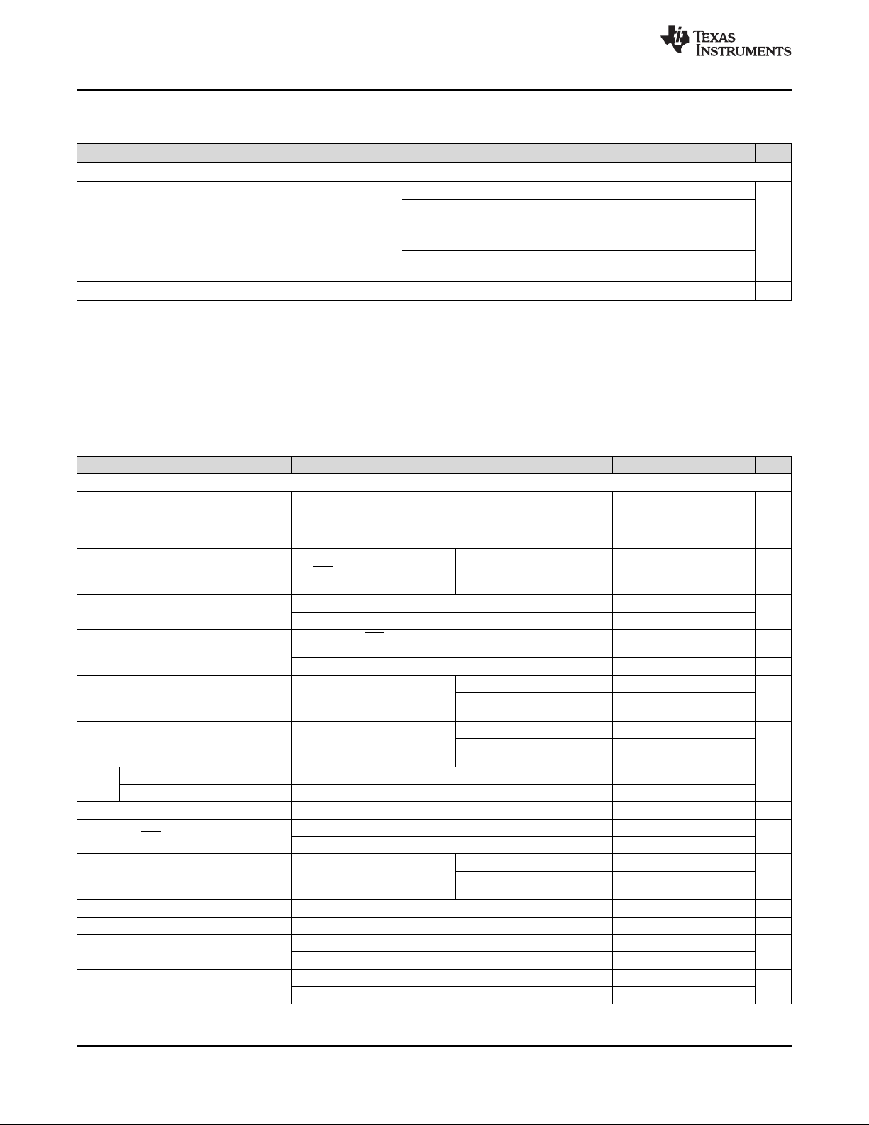
6 Pin Configuration and Functions
D or P Package
8-Pin SOIC or PDIP
Top View
PIN
NAME SOIC, PDIP WSON
I/O DESCRIPTION
CB 1 1 I
SS 2 4 I
SYNC 3 6 I
FB 4 8 I
ON/OFF 5 9 I
VSW 8 15, 16 O
GND 6 11, 12 —
VIN 7 14 I
NC —
2, 3, 5, 7,
10, 13
Pin Functions
Bootstrap capacitor connection for high-side driver. Connect a high-quality,
100-nF capacitor from CB to VSW Pin.
Soft-start Pin. Connect a capacitor from this pin to GND to control the output
voltage ramp. If the feature not desired, the pin can be left floating.
This input allows control of the switching clock frequency. If left open-circuited
the regulator is switched at the internal oscillator frequency, typically 260 kHz.
Feedback sense input pin. Connect to the midpoint of feedback divider to set
VOUT for ADJ version or connect this pin directly to the output capacitor for a
fixed output version.
Enable input to the voltage regulator. High = ON and low = OFF. Pull this pin
high or float to enable the regulator
Source pin of the internal high-side FET. This is a switching node. Attached this
pin to an inductor and the cathode of the external diode.
Power ground pins. Connect to system ground. Ground pins of CINand C
Path to CINmust be as short as possible.
Supply input pin to collector pin of high-side FET. Connect to power supply and
input bypass capacitors CIN. Path from VIN pin to high frequency bypass C
and GND must be as short as possible.
— No connect pins
NHN Package
16-Pin WSON
Top View
Connect DAP to pin 11 and 12
OUT
.
IN
Product Folder Links: LM2671
Submit Documentation FeedbackCopyright © 1998–2016, Texas Instruments Incorporated
3
Page 4

LM2671
SNVS008L –SEPTEMBER 1998–REVISED JUNE 2016
www.ti.com
7 Specifications
7.1 Absolute Maximum Ratings
over operating free-air temperature range (unless otherwise noted)
Supply voltage 45 V
ON/OFF pin voltage, V
Switch voltage to ground –1 V
Boost pin voltage VSW+ 8 V
Feedback pin voltage, V
Power dissipation Internally Limited
Lead temperature
Maximum junction temperature 150 °C
Storage temperature, T
(1) Stresses beyond those listed under Absolute Maximum Ratings may cause permanent damage to the device. These are stress ratings
only, which do not imply functional operation of the device at these or any other conditions beyond those indicated under Recommended
Operating Conditions. Exposure to absolute-maximum-rated conditions for extended periods may affect device reliability.
(2) If Military/Aerospace specified devices are required, please contact the Texas Instruments Sales Office/Distributors for availability and
specifications.
SH
FB
D package
Vapor phase (60 s) 215
Infrared (15 s) 220
P package (soldering, 10 s) 260
WSON package See AN-1187
stg
(1)(2)
MIN MAX UNIT
−0.1 6 V
−0.3 14 V
°C
−65 150 °C
7.2 ESD Ratings
VALUE UNIT
V
(ESD)
Electrostatic discharge Human-body model (HBM), per ANSI/ESDA/JEDEC JS-001
(1)(2)
±2000 V
(1) JEDEC document JEP155 states that 500-V HBM allows safe manufacturing with a standard ESD control process.
(2) The human body model is a 100-pF capacitor discharged through a 1.5-kΩ resistor into each pin.
7.3 Recommended Operating Conditions
MIN MAX UNIT
Supply voltage 6.5 40 V
Junction temperature, T
J
–40 125 °C
7.4 Thermal Information
LM2674
THERMAL METRIC
R
θJA
Junction-to-ambient thermal resistance
(1) For more information about traditional and new thermal metrics, see the Semiconductor and IC Package Thermal Metrics application
report.
(2) Junction to ambient thermal resistance with approximately 1 square inch of printed-circuit board copper surrounding the leads. Additional
copper area lowers thermal resistance further. The value R
area, trace material, and the number of layers and thermal vias. For improved thermal resistance and power dissipation for the WSON
package, see AN-1187 Leadless Leadframe Package (LLP).
(1)
UNITD (SOIC) P (PDIP) NHN (WSON)
8 PINS 8 PINS 16 PINS
(2)
for the WSON (NHN) package is specifically dependent on PCB trace
θJA
105 95 — °C/W
4
Submit Documentation Feedback Copyright © 1998–2016, Texas Instruments Incorporated
Product Folder Links: LM2671
Page 5

LM2671
www.ti.com
SNVS008L –SEPTEMBER 1998–REVISED JUNE 2016
7.5 Electrical Characteristics – 3.3 V
Specifications are for TJ= 25°C (unless otherwise noted).
PARAMETER TEST CONDITIONS MIN
SYSTEM PARAMETERS
V
Output voltage
OUT
η Efficiency VIN= 12 V, I
(3)
VIN= 8 V to 40 V,
I
= 20 mA to 500 mA
LOAD
VIN= 6.5 V to 40 V,
I
= 20 mA to 250 mA
LOAD
LOAD
TJ= 25°C 3.251 3.3 3.35
Over full operating temperature
range
TJ= 25°C 3.251 3.3 3.35
Over full operating temperature
range
= 500 mA 86%
(1)
3.201 3.399
3.201 3.399
(1) All room temperature limits are 100% production tested. All limits at temperature extremes are ensured through correlation using
standard Statistical Quality Control (SQC) methods. All limits are used to calculate Average Outgoing Quality Level (AOQL).
(2) Typical numbers are at 25°C and represent the most likely norm.
(3) External components such as the catch diode, inductor, input and output capacitors, and voltage programming resistors can affect
switching regulator performance. When the LM2671 is used as shown in Figure 15 and Figure 21 test circuits, system performance is as
specified by the system parameters section of the Electrical Characteristics.
TYP
(2)
MAX
(1)
7.6 Electrical Characteristics – 5 V
Specifications are for TJ= 25°C (unless otherwise noted).
PARAMETER TEST CONDITIONS MIN
SYSTEM PARAMETERS
V
Output voltage
OUT
η Efficiency VIN= 12 V, I
(3)
VIN= 8 V to 40 V,
I
= 20 mA to 500 mA
LOAD
VIN= 6.5 V to 40 V,
I
= 20 mA to 250 mA
LOAD
LOAD
TJ= 25°C 4.925 5 5.075
Over full operating temperature
range
TJ= 25°C 4.925 5 5.075
Over full operating temperature
range
= 500 mA 90%
(1)
4.85 5.15
4.85 5.15
(1) All room temperature limits are 100% production tested. All limits at temperature extremes are ensured through correlation using
standard Statistical Quality Control (SQC) methods. All limits are used to calculate Average Outgoing Quality Level (AOQL).
(2) Typical numbers are at 25°C and represent the most likely norm.
(3) External components such as the catch diode, inductor, input and output capacitors, and voltage programming resistors can affect
switching regulator performance. When the LM2671 is used as shown in Figure 15 and Figure 21 test circuits, system performance is as
specified by the system parameters section of the Electrical Characteristics.
TYP
(2)
MAX
(1)
UNIT
V
V
UNIT
V
V
7.7 Electrical Characteristics – 12 V
Specifications are for TJ= 25°C (unless otherwise noted).
PARAMETER TEST CONDITIONS MIN
SYSTEM PARAMETERS
V
Output voltage
OUT
η Efficiency VIN= 24 V, I
(3)
VIN= 15 V to 40 V,
I
= 20 mA to 500 mA
LOAD
LOAD
TJ= 25°C 11.82 12 12.18
Over full operating
temperature range
= 500 mA 94%
(1)
11.64 12.36
(1) All room temperature limits are 100% production tested. All limits at temperature extremes are ensured through correlation using
standard Statistical Quality Control (SQC) methods. All limits are used to calculate Average Outgoing Quality Level (AOQL).
(2) Typical numbers are at 25°C and represent the most likely norm.
(3) External components such as the catch diode, inductor, input and output capacitors, and voltage programming resistors can affect
switching regulator performance. When the LM2671 is used as shown in Figure 15 and Figure 21 test circuits, system performance is as
specified by the system parameters section of the Electrical Characteristics.
Submit Documentation FeedbackCopyright © 1998–2016, Texas Instruments Incorporated
Product Folder Links: LM2671
TYP
(2)
MAX
(1)
UNIT
V
5
Page 6
LM2671
SNVS008L –SEPTEMBER 1998–REVISED JUNE 2016
www.ti.com
7.8 Electrical Characteristics – Adjustable
Specifications are for TJ= 25°C (unless otherwise noted).
PARAMETER TEST CONDITIONS MIN
SYSTEM PARAMETERS
Feedback
V
FB
voltage
η Efficiency VIN= 12 V, I
(3)
VIN= 8 V to 40 V,
I
= 20 mA to 500 mA
LOAD
V
programmed for 5 V
OUT
VIN= 6.5 V to 40 V,
I
= 20 mA to 250 mA
LOAD
V
programmed for 5 V
OUT
LOAD
TJ= 25°C 1.192 1.21 1.228
Over full operating
temperature range
TJ= 25°C 1.192 1.21 1.228
Over full operating
temperature range
= 500 mA 90%
(1)
1.174 1.246
1.174 1.246
(1) All room temperature limits are 100% production tested. All limits at temperature extremes are ensured through correlation using
standard Statistical Quality Control (SQC) methods. All limits are used to calculate Average Outgoing Quality Level (AOQL).
(2) Typical numbers are at 25°C and represent the most likely norm.
(3) External components such as the catch diode, inductor, input and output capacitors, and voltage programming resistors can affect
switching regulator performance. When the LM2671 is used as shown in Figure 15 and Figure 21 test circuits, system performance is as
specified by the system parameters section of the Electrical Characteristics.
TYP
(2)
MAX
(1)
UNIT
7.9 Electrical Characteristics – All Output Voltage Versions
Specifications are for TJ= 25°C, VIN= 12 V for the 3.3-V, 5-V, and Adjustable versions and VIN= 24 V for the 12-V version,
and I
DEVICE PARAMETERS
I
Q
I
STBY
I
CL
I
L
R
DS(ON)
f
O
D
I
BIAS
V
S/D
I
S/D
F
SYNC
V
SYNC
V
SS
I
SS
= 100 mA (unless otherwise noted).
LOAD
PARAMETERS TEST CONDITIONS MIN TYP MAX UNIT
V
Quiescent current
Standby quiescent current ON/OFF pin = 0 V
Current limit
Output leakage current
Switch ON-resistance I
Oscillator frequency Measured at switch pin
Maximum duty cycle 95%
Minimum duty cycle 0%
Feedback bias current V
ON/OFF pin voltage thresholds
ON/OFF pin current ON/OFF pin = 0 V
Synchronization frequency V
Synchronization threshold voltage 1.4 V
Soft-start voltage
Soft-start current
for 3.3-V, 5-V, and adjustable versions
V
for 12-V versions
TJ= 25°C 0.62 0.8 1.2
Over full operating temperature range 0.575 1.25
VIN= 40 V, ON/OFF pin = 0 V
V
V
SWITCH
TJ= 25°C 1.4
Over full operating temperature range 0.8 2
TJ= 25°C 0.63
Over full operating temperature range 0.53 0.73
TJ= 25°C 4.5
Over full operating temperature range 1.5 6.9
= 8 V
FEEDBACK
= 15 V
FEEDBACK
TJ= 25°C 50 100
Over full operating temperature
range
= 0 V
SWITCH
= −1 V, ON/OFF pin = 0 V 6 15 mA
SWITCH
TJ= 25°C 0.25 0.4
= 500 mA
= 1.3 V (adjustable version only) 85 nA
FEEDBACK
= 3.5 V, 50% duty cycle 400 kHz
SYNC
Over full operating temperature
range
TJ= 25°C 260
Over full operating temperature
range
TJ= 25°C 20
Over full operating temperature
range
225 275
2.5 3.6
2.5
1 25 μA
7 37
150
0.6
V
V
mA
μA
A
Ω
kHz
V
μA
V
μA
6
Submit Documentation Feedback Copyright © 1998–2016, Texas Instruments Incorporated
Product Folder Links: LM2671
Page 7

www.ti.com
7.10 Typical Characteristics
LM2671
SNVS008L –SEPTEMBER 1998–REVISED JUNE 2016
Figure 1. Normalized Output Voltage
Figure 3. Efficiency
Figure 2. Line Regulation
Figure 4. Drain-to-Source Resistance
Figure 5. Switch Current Limit
Product Folder Links: LM2671
Figure 6. Operating Quiescent Current
Submit Documentation FeedbackCopyright © 1998–2016, Texas Instruments Incorporated
7
Page 8

LM2671
SNVS008L –SEPTEMBER 1998–REVISED JUNE 2016
Typical Characteristics (continued)
www.ti.com
Figure 7. Standby Quiescent Current
Figure 9. ON/OFF Pin Current (Sourcing) Figure 10. Switching Frequency
Figure 8. ON/OFF Threshold Voltage
Figure 11. Feedback Pin Bias Current Figure 12. Peak Switch Current
8
Submit Documentation Feedback Copyright © 1998–2016, Texas Instruments Incorporated
Product Folder Links: LM2671
Page 9

www.ti.com
Typical Characteristics (continued)
Figure 13. Dropout Voltage – 3.3-V Option Figure 14. Dropout Voltage – 5-V Option
LM2671
SNVS008L –SEPTEMBER 1998–REVISED JUNE 2016
Product Folder Links: LM2671
Submit Documentation FeedbackCopyright © 1998–2016, Texas Instruments Incorporated
9
Page 10
LM2671
SNVS008L –SEPTEMBER 1998–REVISED JUNE 2016
www.ti.com
8 Detailed Description
8.1 Overview
The LM2671 provides all of the active functions required for a step-down (buck) switching regulator. The internal
power switch is a DMOS power MOSFET to provide power supply designs with high current capability, up to
0.5 A, and highly efficient operation.
The LM2671 is part of the SIMPLE SWITCHER®family of power converters. A complete design uses a minimum
number of external components, which have been predetermined from a variety of manufacturers. Using either
this data sheet or TI's WEBENCH®design tool, a complete switching power supply can be designed quickly.
Also, see LM2670 SIMPLE SWITCHER®High Efficiency 3A Step-Down Voltage Regulator with Sync for
additional applications information.
8.2 Functional Block Diagram
8.3 Feature Description
8.3.1 Switch Output
This is the output of a power MOSFET switch connected directly to the input voltage. The switch provides energy
to an inductor, an output capacitor and the load circuitry under control of an internal pulse-width-modulator
(PWM). The PWM controller is internally clocked by a fixed 260-kHz oscillator. In a standard step-down
application the duty cycle (Time ON/Time OFF) of the power switch is proportional to the ratio of the power
supply output voltage to the input voltage. The voltage on the VSWpin cycles between VIN(switch ON) and below
ground by the voltage drop of the external Schottky diode (switch OFF).
10
Submit Documentation Feedback Copyright © 1998–2016, Texas Instruments Incorporated
Product Folder Links: LM2671
Page 11

LM2671
www.ti.com
SNVS008L –SEPTEMBER 1998–REVISED JUNE 2016
Feature Description (continued)
8.3.2 Input
The input voltage for the power supply is connected to the VINpin. In addition to providing energy to the load the
input voltage also provides bias for the internal circuitry of the LM2671. For ensured performance the input
voltage must be in the range of 6.5 V to 40 V. For best performance of the power supply the VINpin must always
be bypassed with an input capacitor placed close to this pin and GND.
8.3.3 C Boost
A capacitor must be connected from the CBpin to the VSWpin. This capacitor boosts the gate drive to the internal
MOSFET above VINto fully turn it ON. This minimizes conduction losses in the power switch to maintain high
efficiency. The recommended value for C Boost is 0.01 μF.
8.3.4 Ground
This is the ground reference connection for all components in the power supply. In fast-switching, high-current
applications such as those implemented with the LM2671, TI recommends that a broad ground plane be used to
minimize signal coupling throughout the circuit.
8.3.5 Sync
This input allows control of the switching clock frequency. If left open-circuited the regulator is switched at the
internal oscillator frequency, typically 260 kHz. An external clock can be used to force the switching frequency
and thereby control the output ripple frequency of the regulator. This capability provides for consistent filtering of
the output ripple from system to system as well as precise frequency spectrum positioning of the ripple frequency
which is often desired in communications and radio applications. This external frequency must be greater than
the LM2671 internal oscillator frequency, which could be as high as 275 kHz, to prevent an erroneous reset of
the internal ramp oscillator and PWM control of the power switch. The ramp oscillator is reset on the positive
going edge of the sync input signal. TI recommends that the external TTL or CMOS compatible clock (between
0 V and a level greater than 3 V) be ac coupled to the SYNC pin through a 100-pF capacitor and a 1-kΩ resistor
to ground.
When the SYNC function is used, current limit frequency foldback is not active. Therefore, the device may not be
fully protected against extreme output short-circuit conditions.
8.3.6 Feedback
This is the input to a two-stage high gain amplifier, which drives the PWM controller. Connect the FB pin directly
to the output for proper regulation. For the fixed output devices (3.3-V, 5-V and 12-V outputs), a direct wire
connection to the output is all that is required as internal gain setting resistors are provided inside the LM2671.
For the adjustable output version two external resistors are required to set the DC output voltage. For stable
operation of the power supply it is important to prevent coupling of any inductor flux to the feedback input.
8.3.7 ON/OFF
This input provides an electrical ON/OFF control of the power supply. Connecting this pin to ground or to any
voltage less than 0.8 V is completely turn OFF the regulator. The current drain from the input supply when OFF
is only 50 μA. The ON/OFF input has an internal pullup current source of approximately 20 μA and a protection
clamp Zener diode of 7 V to ground. When electrically driving the ON/OFF pin the high voltage level for the ON
condition must not exceed the 6 V absolute maximum limit. When ON/OFF control is not required this pin must
be left open.
8.4 Device Functional Modes
8.4.1 Shutdown Mode
The ON/OFF pin provides electrical ON and OFF control for the LM2671. When the voltage of this pin is lower
than 1.4 V, the device enters shutdown mode. The typical standby current in this mode is 50 μA.
Submit Documentation FeedbackCopyright © 1998–2016, Texas Instruments Incorporated
Product Folder Links: LM2671
11
Page 12

LM2671
SNVS008L –SEPTEMBER 1998–REVISED JUNE 2016
www.ti.com
Device Functional Modes (continued)
8.4.2 Active Mode
When the voltage of the ON/OFF pin is higher than 1.4 V, the device starts switching and the output voltage rises
until it reaches a normal regulation voltage.
12
Submit Documentation Feedback Copyright © 1998–2016, Texas Instruments Incorporated
Product Folder Links: LM2671
Page 13
LM2671
www.ti.com
SNVS008L –SEPTEMBER 1998–REVISED JUNE 2016
9 Application and Implementation
NOTE
Information in the following applications sections is not part of the TI component
specification, and TI does not warrant its accuracy or completeness. TI’s customers are
responsible for determining suitability of components for their purposes. Customers should
validate and test their design implementation to confirm system functionality.
9.1 Application Information
The LM2671 is a step-down DC-DC regulator. The device is typically used to convert a higher DC voltage to a
lower DC voltage with a maximum output current of 0.5 A. The following design procedure can be used to select
components for the LM2671. Alternately, the WEBENCH®software may be used to generate complete designs.
When generating a design, the WEBENCH software uses iterative design procedure and accesses
comprehensive databases of components. See ti.com for more details.
When the output voltage is greater than approximately 6 V, and the duty cycle at minimum input voltage is
greater than approximately 50%, the designer must exercise caution in selection of the output filter components.
When an application designed to these specific operating conditions is subjected to a current limit fault condition,
it may be possible to observe a large hysteresis in the current limit. This can affect the output voltage of the
device until the load current is reduced sufficiently to allow the current limit protection circuit to reset itself.
Under current limiting conditions, the LM267x is designed to respond in the following manner:
1. At the moment when the inductor current reaches the current limit threshold, the ON-pulse is immediately
terminated. This happens for any application condition.
2. However, the current limit block is also designed to momentarily reduce the duty cycle to below 50% to avoid
subharmonic oscillations, which could cause the inductor to saturate.
3. Therefore, once the inductor current falls below the current limit threshold, there is a small relaxation time
during which the duty cycle progressively rises back above 50% to the value required to achieve regulation.
If the output capacitance is sufficiently large, it might be possible that as the output tries to recover, the output
capacitor charging current is large enough to repeatedly re-trigger the current limit circuit before the output has
fully settled. This condition is exacerbated with higher output voltage settings because the energy requirement of
the output capacitor varies as the square of the output voltage (½ CV2), thus requiring an increased charging
current. A simple test to determine if this condition might exist for a suspect application is to apply a short circuit
across the output of the converter, and then remove the shorted output condition. In an application with properly
selected external components, the output recovers smoothly. Practical values of external components that have
been experimentally found to work well under these specific operating conditions are C
= 47 µF, L = 22 µH.
OUT
NOTE
Even with these components, for a device’s current limit of ICLIM, the maximum load
current under which the possibility of the large current limit hysteresis can be minimized is
ICLIM/2.
For example, if the input is 24 V and the set output voltage is 18 V, then for a desired maximum current of 1.5 A,
the current limit of the chosen switcher must be confirmed to be at least 3 A. Under extreme overcurrent or shortcircuit conditions, the LM267X employs frequency foldback in addition to the current limit. If the cycle-by-cycle
inductor current increases above the current limit threshold (due to short circuit or inductor saturation for
example) the switching frequency is automatically reduced to protect the IC. Frequency below 100 kHz is typical
for an extreme short-circuit condition.
Submit Documentation FeedbackCopyright © 1998–2016, Texas Instruments Incorporated
Product Folder Links: LM2671
13
Page 14

LM2671
SNVS008L –SEPTEMBER 1998–REVISED JUNE 2016
9.2 Typical Applications
9.2.1 Fixed Output Voltage Version
CIN= 22-μF, 50-V Tantalum, Sprague 199D Series
C
= 47-μF, 25-V Tantalum, Sprague 595D Series
OUT
D1 = 3.3-A, 50-V Schottky Rectifier, IR 30WQ05F
L1 = 68-μH Sumida #RCR110D-680L
CB= 0.01-μF, 50-V ceramic
Figure 15. Typical Application for Fixed Output Voltage Versions
9.2.1.1 Design Requirements
Table 1 lists the design parameters for this example.
www.ti.com
Table 1. Design Parameters
PARAMETER VALUE
Regulated output voltage (3.3 V, 5 V, or 12 V), V
Maximum DC input voltage, VIN(max) 12 V
Maximum load current, I
(max) 500 mA
LOAD
OUT
5 V
9.2.1.2 Detailed Design Procedure
9.2.1.2.1 Inductor Selection (L1)
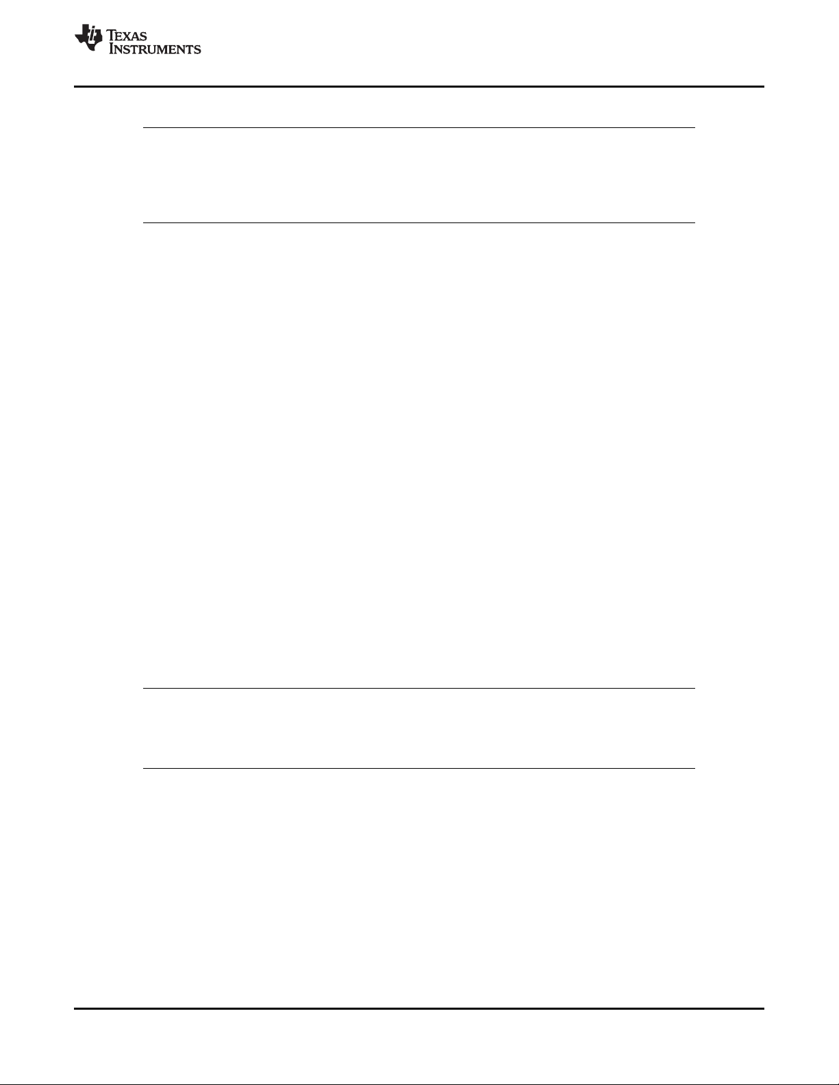
1. Select the correct inductor value selection guide from Figure 17 and Figure 18 or Figure 19 (output voltages
of 3.3 V, 5 V, or 12 V respectively). For all other voltages, see the design procedure for the adjustable
version. Use the inductor selection guide for the 5-V version shown in Figure 18.
2. From the inductor value selection guide, identify the inductance region intersected by the maximum input
voltage line and the maximum load current line. Each region is identified by an inductance value and an
inductor code (LXX). From the inductor value selection guide shown in Figure 18, the inductance region
intersected by the 12-V horizontal line and the 500-mA vertical line is 47 μH, and the inductor code is L13.
3. Select an appropriate inductor from the four manufacturer's part numbers listed in Table 2. Each
manufacturer makes a different style of inductor to allow flexibility in meeting various design requirements.
See the following for some of the differentiating characteristics of each manufacturer's inductors:
– Schottky: ferrite EP core inductors; these have very low leakage magnetic fields to reduce electro-
magnetic interference (EMI) and are the lowest power loss inductors
– Renco: ferrite stick core inductors; benefits are typically lowest cost inductors and can withstand E•T and
transient peak currents above rated value. Be aware that these inductors have an external magnetic field
which may generate more EMI than other types of inductors.
– Pulse: powered iron toroid core inductors; these can also be low cost and can withstand larger than
normal E•T and transient peak currents. Toroid inductors have low EMI.
– Coilcraft: ferrite drum core inductors; these are the smallest physical size inductors, available only as
SMT components. Be aware that these inductors also generate EMI—but less than stick inductors.
Complete specifications for these inductors are available from the respective manufacturers.
14
Submit Documentation Feedback Copyright © 1998–2016, Texas Instruments Incorporated
Product Folder Links: LM2671
Page 15

LM2671
www.ti.com
SNVS008L –SEPTEMBER 1998–REVISED JUNE 2016
The inductance value required is 47 μH. From the table in Table 2, go to the L13 line and choose an inductor
part number from any of the four manufacturers shown. In most instances, both through hole and surface mount
inductors are available.
Table 2. Inductor Manufacturers' Part Numbers
IND.
INDUCTANCE
REF.
DESG.
L2 150 0.21 67143920 67144290 RL-5470-4 RL1500-150 PE-53802 PE-53802-S DO1608-154
L3 100 0.26 67143930 67144300 RL-5470-5 RL1500-100 PE-53803 PE-53803-S DO1608-104
L4 68 0.32 67143940 67144310 RL-1284-68-43 RL1500-68 PE-53804 PE-53804-S DO1608-683
L5 47 0.37 67148310 67148420 RL-1284-47-43 RL1500-47 PE-53805 PE-53805-S DO1608-473
L6 33 0.44 67148320 67148430 RL-1284-33-43 RL1500-33 PE-53806 PE-53806-S DO1608-333
L7 22 0.52 67148330 67148440 RL-1284-22-43 RL1500-22 PE-53807 PE-53807-S DO1608-223
L9 220 0.32 67143960 67144330 RL-5470-3 RL1500-220 PE-53809 PE-53809-S DO3308-224
L10 150 0.39 67143970 67144340 RL-5470-4 RL1500-150 PE-53810 PE-53810-S DO3308-154
L11 100 0.48 67143980 67144350 RL-5470-5 RL1500-100 PE-53811 PE-53811-S DO3308-104
L12 68 0.58 67143990 67144360 RL-5470-6 RL1500-68 PE-53812 PE-53812-S DO3308-683
L13 47 0.7 67144000 67144380 RL-5470-7 RL1500-47 PE-53813 PE-53813-S DO3308-473
L14 33 0.83 67148340 67148450 RL-1284-33-43 RL1500-33 PE-53814 PE-53814-S DO3308-333
L15 22 0.99 67148350 67148460 RL-1284-22-43 RL1500-22 PE-53815 PE-53815-S DO3308-223
L18 220 0.55 67144040 67144420 RL-5471-2 RL1500-220 PE-53818 PE-53818-S DO3316-224
L19 150 0.66 67144050 67144430 RL-5471-3 RL1500-150 PE-53819 PE-53819-S DO3316-154
L20 100 0.82 67144060 67144440 RL-5471-4 RL1500-100 PE-53820 PE-53820-S DO3316-104
L21 68 0.99 67144070 67144450 RL-5471-5 RL1500-68 PE-53821 PE-53821-S DO3316-683
(μH)
CURRENT
(A)
SCHOTTKY RENCO PULSE ENGINEERING COILCRAFT
THROUGH
HOLE
SURFACE
MOUNT
THROUGH HOLE
SURFACE
MOUNT
THROUGH
HOLE
SURFACE
MOUNT
SURFACE
MOUNT
9.2.1.2.2 Output Capacitor Selection (C
OUT
)
Select an output capacitor from the output capacitor table in Table 9. Using the output voltage and the
inductance value found in the inductor selection guide, step 1, locate the appropriate capacitor value and voltage
rating.
Use the 5-V section in the output capacitor table in Table 9. Choose a capacitor value and voltage rating from
the line that contains the inductance value of 47 μH. The capacitance and voltage rating values corresponding to
the 47-μH inductor are:
• Surface mount:
– 68-μF, 10-V Sprague 594D series
– 100-μF, 10-V AVX TPS series
• Through hole:
– 68-μF, 10-V Sanyo OS-CON SA series
– 150-μF, 35-V Sanyo MV-GX series
– 150-μF, 35-V Nichicon PL series
– 150-μF, 35-V Panasonic HFQ series
The capacitor list contains through-hole electrolytic capacitors from four different capacitor manufacturers and
surface mount tantalum capacitors from two different capacitor manufacturers. TI recommends that both the
manufacturers and the manufacturer's series that are listed in the table be used.
Product Folder Links: LM2671
Submit Documentation FeedbackCopyright © 1998–2016, Texas Instruments Incorporated
15
Page 16

LM2671
SNVS008L –SEPTEMBER 1998–REVISED JUNE 2016
OUTPUT
VOLTAGE
(V)
3.3
5
12
INDUCTANCE
(μH)
22 120/6.3 100/10 100/10 330/35 330/35 330/35
33 120/6.3 100/10 68/10 220/35 220/35 220/35
47 68/10 100/10 68/10 150/35 150/35 150/35
68 120/6.3 100/10 100/10 120/35 120/35 120/35
100 120/6.3 100/10 100/10 120/35 120/35 120/35
150 120/6.3 100/10 100/10 120/35 120/35 120/35
22 100/16 100/10 100/10 330/35 330/35 330/35
33 68/10 10010 68/10 220/35 220/35 220/35
47 68/10 100/10 68/10 150/35 150/35 150/35
68 100/16 100/10 100/10 120/35 120/35 120/35
100 100/16 100/10 100/10 120/35 120/35 120/35
150 100/16 100/10 100/10 120/35 120/35 120/35
22 120/20 (2×) 68/20 68/20 330/35 330/35 330/35
33 68/25 68/20 68/20 220/35 220/35 220/35
47 47/20 68/20 47/20 150/35 150/35 150/35
68 47/20 68/20 47/20 120/35 120/35 120/35
100 47/20 68/20 47/20 120/35 120/35 120/35
150 47/20 68/20 47/20 120/35 120/35 120/35
220 47/20 68/20 47/20 120/35 120/35 120/35
SURFACE MOUNT THROUGH HOLE
SPRAGUE
594D SERIES
(μF/V)
Table 3. Output Capacitor Table
OUTPUT CAPACITOR
AVX TPS
SERIES
(μF/V)
SANYO OS-CON
SA SERIES (μF/V)
SANYO MV-GX
SERIES (μF/V)
NICHICON
PL SERIES
(μF/V)
www.ti.com
PANASONIC
HFQ SERIES
(μF/V)
9.2.1.2.3 Catch Diode Selection (D1)
1. In normal operation, the average current of the catch diode is the load current times the catch diode duty
cycle, 1-D (D is the switch duty cycle, which is approximately the output voltage divided by the input voltage).
The largest value of the catch diode average current occurs at the maximum load current and maximum
input voltage (minimum D). For normal operation, the catch diode current rating must be at least 1.3 times
greater than its maximum average current. However, if the power supply design must withstand a continuous
output short, the diode must have a current rating equal to the maximum current limit of the LM2671. The
most stressful condition for this diode is a shorted output condition (refer to Table 4). In this example, a 1-A,
20-V Schottky diode provides the best performance. If the circuit must withstand a continuous shorted output,
TI recommends a higher-current Schottky diode.
2. The reverse voltage rating of the diode must be at least 1.25 times the maximum input voltage.
3. Because of their fast switching speed and low forward voltage drop, Schottky diodes provide the best
performance and efficiency. This Schottky diode must be placed close to the LM2671 using short leads and
short printed-circuit traces.
16
Submit Documentation Feedback Copyright © 1998–2016, Texas Instruments Incorporated
Product Folder Links: LM2671
Page 17

LM2671
www.ti.com
SNVS008L –SEPTEMBER 1998–REVISED JUNE 2016
Table 4. Schottky Diode Selection Table
V
R
20 V
30 V
40 V
50 V
SURFACE MOUNT THROUGH HOLE SURFACE MOUNT THROUGH HOLE
SK12 1N5817 SK32 1N5820
B120 SR102 — SR302
SK13 1N5818 SK33 1N5821
B130 11DQ03 30WQ03F 31DQ03
MBRS130 SR103 — —
SK14 1N5819 SK34 1N5822
B140 11DQ04 30BQ040 MBR340
MBRS140 SR104 30WQ04F 31DQ04
10BQ040 — MBRS340 SR304
10MQ040 — MBRD340 —
15MQ040 — — —
SK15 MBR150 SK35 MBR350
B150 11DQ05 30WQ05F 31DQ05
10BQ050 SR105 — SR305
9.2.1.2.4 Input Capacitor (CIN)
1-A DIODES 3-A DIODES
A low ESR aluminum or tantalum bypass capacitor is required between the input pin and ground to prevent large
voltage transients from appearing at the input. This capacitor must be placed close to the IC using short leads. In
addition, the RMS current rating of the input capacitor must be selected to be at least ½ the DC load current. The
capacitor manufacturer data sheet must be checked to assure that this current rating is not exceeded. The
curves shown in Figure 16 show typical RMS current ratings for several different aluminum electrolytic capacitor
values. A parallel connection of two or more capacitors may be required to increase the total minimum RMS
current rating to suit the application requirements.
For an aluminum electrolytic capacitor, the voltage rating must be at least 1.25 times the maximum input voltage.
Caution must be exercised if solid tantalum capacitors are used. The tantalum capacitor voltage rating must be
twice the maximum input voltage. Table 5 and Table 6 show the recommended application voltage for AVX TPS
and Sprague 594D tantalum capacitors. TI also recommends that they be surge current tested by the
manufacturer. The TPS series available from AVX, and the 593D and 594D series from Sprague are all surge
current tested. Another approach to minimize the surge current stresses on the input capacitor is to add a small
inductor in series with the input supply line.
Table 5. AVX TPS
RECOMMENDED
APPLICATION VOLTAGE
3.3 6.3
5 10
10 20
12 25
15 35
Product Folder Links: LM2671
85°C RATING
VOLTAGE
RATING
Submit Documentation FeedbackCopyright © 1998–2016, Texas Instruments Incorporated
17
Page 18

LM2671
SNVS008L –SEPTEMBER 1998–REVISED JUNE 2016
RECOMMENDED
APPLICATION VOLTAGE
www.ti.com
Table 6. Sprague 594D
VOLTAGE
RATING
85°C RATING
2.5 4
3.3 6.3
5 10
8 16
12 20
18 25
24 35
29 50
Use caution when using ceramic capacitors for input bypassing, because it may cause severe ringing at the V
pin. The important parameters for the input capacitor are the input voltage rating and the RMS current rating.
With a maximum input voltage of 12 V, an aluminum electrolytic capacitor with a voltage rating greater than 15 V
(1.25 × VIN) is required. The next higher capacitor voltage rating is 16 V.
The RMS current rating requirement for the input capacitor in a buck regulator is approximately ½ the DC load
current. In this example, with a 500-mA load, a capacitor with a RMS current rating of at least 250 mA is
required. The curves shown in Figure 16 can be used to select an appropriate input capacitor. From the curves,
locate the 16-V line and note which capacitor values have RMS current ratings greater than 250 mA.
Figure 16. RMS Current Ratings for Low ESR Electrolytic Capacitors (Typical)
IN
For a through-hole design, a 100-μF, 16-V electrolytic capacitor (Panasonic HFQ series, Nichicon PL, Sanyo MVGX series or equivalent) would be adequate. Other types or other manufacturers' capacitors can be used
provided the RMS ripple current ratings are adequate. Additionally, for a complete surface mount design,
electrolytic capacitors such as the Sanyo CV-C or CV-BS and the Nichicon WF or UR and the NIC Components
NACZ series could be considered.
For surface mount designs, solid tantalum capacitors can be used, but caution must be exercised with regard to
the capacitor surge current rating and voltage rating. In this example, checking the Sprague 594D series
datasheet, a Sprague 594D 15-μF, 25-V capacitor is adequate.
9.2.1.2.5 Boost Capacitor (CB)
This capacitor develops the necessary voltage to turn the switch gate on fully. All applications must use a
0.01-μF, 50-V ceramic capacitor. For this application, and all applications, use a 0.01-μF, 50-V ceramic capacitor.
18
Submit Documentation Feedback Copyright © 1998–2016, Texas Instruments Incorporated
Product Folder Links: LM2671
Page 19

LM2671
www.ti.com
9.2.1.2.6 Soft-Start Capacitor (CSS) – Optional
SNVS008L –SEPTEMBER 1998–REVISED JUNE 2016
This capacitor controls the rate at which the device starts up. The formula for the soft-start capacitor CSSis
Equation 1.
where
• ISS= soft-start current (4.5 μA typical)
• tSS= soft-start time (selected)
• V
• V
• V
• VIN= input voltage (selected) (1)
= soft-start threshold voltage (0.63 V typical)
SSTH
= output voltage (selected)
OUT
SCHOTTKY
= schottky diode voltage drop (0.4 V typical)
For this application, selecting a start-up time of 10 ms and using Equation 2 for CSS.
(2)
If this feature is not desired, leave this pin open. With certain soft-start capacitor values and operating conditions,
the LM2671 can exhibit an overshoot on the output voltage during turnon. Especially when starting up into no
load or low load, the soft-start function may not be effective in preventing a larger voltage overshoot on the
output. With larger loads or lower input voltages during start-up this effect is minimized. In particular, avoid using
soft-start capacitors between 0.033 µF and 1 µF.
9.2.1.2.7 Frequency Synchronization (optional)
The LM2671 (oscillator) can be synchronized to run with an external oscillator, using the sync pin (pin 3). By
doing so, the LM2671 can be operated at higher frequencies than the standard frequency of 260 kHz. This
allows for a reduction in the size of the inductor and output capacitor.
As shown in the drawing below, a signal applied to a RC filter at the sync pin causes the device to synchronize to
the frequency of that signal. For a signal with a peak-to-peak amplitude of 3 V or greater, a 1-kΩ resistor and a
100-pF capacitor are suitable values.
For all applications, use a 1-kΩ resistor and a 100-pF capacitor for the RC filter.
Product Folder Links: LM2671
Submit Documentation FeedbackCopyright © 1998–2016, Texas Instruments Incorporated
19
Page 20
LM2671
SNVS008L –SEPTEMBER 1998–REVISED JUNE 2016
9.2.1.3 Application Curves
for continuous mode operation
www.ti.com
Figure 17. LM2671-3.3
Figure 19. LM2671-12
9.2.2 Adjustable Output Voltage Version
Figure 18. LM2671-5
Figure 20. LM2671-ADJ
20
CIN= 22-μF, 50-V Tantalum, Sprague 199D Series
C
= 47-μF, 25-V Tantalum, Sprague 595D Series
OUT
D1 = 3.3-A, 50-V Schottky Rectifier, IR 30WQ05F
L1 = 68-μH Sumida #RCR110D-680L
R1 =1.5 kΩ, 1%
CB= 0.01-μF, 50-V ceramic
Figure 21. Typical Application for Adjustable Output Voltage Versions
Submit Documentation Feedback Copyright © 1998–2016, Texas Instruments Incorporated
Product Folder Links: LM2671
Page 21

www.ti.com
9.2.2.1 Design Requirements
Table 7 lists the design parameters for this example.
Table 7. Design Parameters
PARAMETER VALUE
Regulated output voltage, V
Maximum input voltage, VIN(max) 28 V
Maximum load current, I
Switching frequency, F Fixed at a nominal 260 kHz
OUT
(max) 500 mA
LOAD
9.2.2.2 Detailed Design Procedure
9.2.2.2.1 Programming Output Voltage
Select R1and R2, as shown in Figure 21.
Use the following formula to select the appropriate resistor values.
where
• V
= 1.21 V (3)
REF
Select R1to be 1 kΩ, 1%. Solve for R2.
LM2671
SNVS008L –SEPTEMBER 1998–REVISED JUNE 2016
20 V
(4)
Select a value for R1between 240 Ω and 1.5 kΩ. The lower resistor values minimize noise pickup in the sensitive
feedback pin. For the lowest temperature coefficient and the best stability with time, use 1% metal film resistors.
(5)
R2= 1 kΩ (16.53 − 1) = 15.53 kΩ, closest 1% value is 15.4 kΩ.
R2= 15.4 kΩ.
9.2.2.2.2 Inductor Selection (L1)
1. Calculate the inductor Volt • microsecond constant E • T (V • μs) from Equation 6.
where
• V
• VD= diode forward voltage drop = 0.5 V (6)
= internal switch saturation voltage = 0.25 V
SAT
Calculate the inductor Volt • microsecond constant (E • T) with Equation 7.
(7)
2. Use the E • T value from the previous formula and match it with the E • T number on the vertical axis of the
inductor value selection guide shown in Figure 20.
E • T = 21.6 (V • μs) (8)
3. On the horizontal axis, select the maximum load current in Equation 9.
I
(max) = 500 mA (9)
LOAD
4. Identify the inductance region intersected by the E • T value and the maximum load current value. Each
region is identified by an inductance value and an inductor code (LXX). From the inductor value selection
guide shown in Figure 20, the inductance region intersected by the 21.6 (V • μs) horizontal line and the 500mA vertical line is 100 μH, and the inductor code is L20.
5. Select an appropriate inductor from the four manufacturer's part numbers listed in Table 2. For information
Submit Documentation FeedbackCopyright © 1998–2016, Texas Instruments Incorporated
Product Folder Links: LM2671
21
Page 22

LM2671
SNVS008L –SEPTEMBER 1998–REVISED JUNE 2016
on the different types of inductors, see the inductor selection in the fixed output voltage design procedure.
From the table in Table 2, locate line L20, and select an inductor part number from the list of manufacturers'
part numbers.
www.ti.com
9.2.2.2.3 Output Capacitor Selection (C
OUT
)
1. Select an output capacitor from the capacitor code selection guide in Table 8. Using the inductance value
found in the inductor selection guide, step 1, locate the appropriate capacitor code corresponding to the
desired output voltage. Use the appropriate row of the capacitor code selection guide, in Table 8. For this
example, use the 15-V to 20-V row. The capacitor code corresponding to an inductance of 100 μH is C20.
2. Select an appropriate capacitor value and voltage rating, using the capacitor code, from the output capacitor
selection table in Table 9. There are two solid tantalum (surface mount) capacitor manufacturers and four
electrolytic (through hole) capacitor manufacturers to choose from. TI recommends using the manufacturers
and the manufacturer's series that are listed in the table.
From the output capacitor selection table in Table 9, choose a capacitor value (and voltage rating) that
intersects the capacitor code(s) selected in section A, C20.
The capacitance and voltage rating values corresponding to the capacitor code C20 are:
– Surface mount:
– 33-μF, 25-V Sprague 594D series
– 33-μF, 25-V AVX TPS series
– Through hole:
– 33-μF, 25-V Sanyo OS-CON SC series
– 120-μF, 35-V Sanyo MV-GX series
– 120-μF, 35-V Nichicon PL series
– 120-μF, 35-V Panasonic HFQ series
Other manufacturers or other types of capacitors may also be used, provided the capacitor specifications
(especially the 100-kHz ESR) closely match the characteristics of the capacitors listed in the output capacitor
table. See the capacitor manufacturers' data sheet for this information.
Table 8. Capacitor Code Selection Guide
CASE
(1)
STYLE
SM and TH 1.21–2.5 — — — — C1 C2 C3
SM and TH 2.5–3.75 — — — C1 C2 C3 C3
SM and TH 3.75–5 — — C4 C5 C6 C6 C6
SM and TH 5–6.25 — C4 C7 C6 C6 C6 C6
SM and TH 6.25–7.5 C8 C4 C7 C6 C6 C6 C6
SM and TH 7.5–10 C9 C10 C11 C12 C13 C13 C13
SM and TH 10–12.5 C14 C11 C12 C12 C13 C13 C13
SM and TH 12.5–15 C15 C16 C17 C17 C17 C17 C17
SM and TH 15–20 C18 C19 C20 C20 C20 C20 C20
SM and TH 20–30 C21 C22 C22 C22 C22 C22 C22
TH 30–37 C23 C24 C24 C25 C25 C25 C25
(1) SM - Surface Mount, TH - Through Hole
OUTPUT
VOLTAGE (V)
22 33 47 68 100 150 220
INDUCTANCE (μH)
22
Submit Documentation Feedback Copyright © 1998–2016, Texas Instruments Incorporated
Product Folder Links: LM2671
Page 23

www.ti.com
SNVS008L –SEPTEMBER 1998–REVISED JUNE 2016
Table 9. Output Capacitor Selection Table
OUTPUT CAPACITOR
CAP.
REF.
DESG.
C1 120/6.3 100/10 100/10 220/35 220/35 220/35
C2 120/6.3 100/10 100/10 150/35 150/35 150/35
C3 120/6.3 100/10 100/35 120/35 120/35 120/35
C4 68/10 100/10 68/10 220/35 220/35 220/35
C5 100/16 100/10 100/10 150/35 150/35 150/35
C6 100/16 100/10 100/10 120/35 120/35 120/35
C7 68/10 100/10 68/10 150/35 150/35 150/35
C8 100/16 100/10 100/10 330/35 330/35 330/35
C9 100/16 100/16 100/16 330/35 330/35 330/35
C10 100/16 100/16 68/16 220/35 220/35 220/35
C11 100/16 100/16 68/16 150/35 150/35 150/35
C12 100/16 100/16 68/16 120/35 120/35 120/35
C13 100/16 100/16 100/16 120/35 120/35 120/35
C14 100/16 100/16 100/16 220/35 220/35 220/35
C15 47/20 68/20 47/20 220/35 220/35 220/35
C16 47/20 68/20 47/20 150/35 150/35 150/35
C17 47/20 68/20 47/20 120/35 120/35 120/35
C18 68/25 (2×) 33/25 47/25
C19 33/25 33/25 33/25
C20 33/25 33/25 33/25
C21 33/35 (2×) 22/25
C22 33/35 22/35
C23
C24
C25
(1) The SC series of Os-Con capacitors (others are SA series)
(2) The voltage ratings of the surface mount tantalum chip and Os-Con capacitors are too low to work at these voltages.
#
SPRAGUE 594D
SERIES (μF/V)
SURFACE MOUNT THROUGH HOLE
AVX TPS SERIES
(μF/V)
(2) (2) (2)
(2) (2) (2)
(2) (2) (2)
SANYO OS-CON SA
SERIES (μF/V)
(1)
(1)
(1)
(2)
(2)
SANYO MV-GX
SERIES (μF/V)
220/35 220/35 220/35
150/35 150/35 150/35
120/35 120/35 120/35
150/35 150/35 150/35
120/35 120/35 120/35
220/50 100/50 120/50
150/50 100/50 120/50
150/50 82/50 82/50
NICHICON PL
SERIES (μF/V)
PANASONIC HFQ
SERIES (μF/V)
LM2671
9.2.2.2.4 Catch Diode Selection (D1)
1. In normal operation, the average current of the catch diode is the load current times the catch diode duty
cycle, 1-D (D is the switch duty cycle, which is approximately V
OUT/VIN
). The largest value of the catch diode
average current occurs at the maximum input voltage (minimum D). For normal operation, the catch diode
current rating must be at least 1.3 times greater than its maximum average current. However, if the power
supply design must withstand a continuous output short, the diode must have a current rating greater than
the maximum current limit of the LM2671. The most stressful condition for this diode is a shorted output
condition.
Refer to the table shown in Table 4. Schottky diodes provide the best performance, and in this example a 1A, 40-V Schottky diode would be a good choice. If the circuit must withstand a continuous shorted output, a
higher current (at least 1.2 A) Schottky diode is recommended.
2. The reverse voltage rating of the diode must be at least 1.25 times the maximum input voltage.
3. Because of their fast switching speed and low forward voltage drop, Schottky diodes provide the best
performance and efficiency. The Schottky diode must be placed close to the LM2671 using short leads and
short printed-circuit traces.
Submit Documentation FeedbackCopyright © 1998–2016, Texas Instruments Incorporated
Product Folder Links: LM2671
23
Page 24
LM2671
SNVS008L –SEPTEMBER 1998–REVISED JUNE 2016
9.2.2.2.5 Input Capacitor (CIN)
www.ti.com
A low ESR aluminum or tantalum bypass capacitor is required between the input pin and ground to prevent large
voltage transients from appearing at the input. This capacitor must be placed close to the IC using short leads. In
addition, the RMS current rating of the input capacitor must be selected to be at least ½ the DC load current. The
capacitor manufacturer data sheet must be checked to assure that this current rating is not exceeded. The
curves shown in Figure 16 show typical RMS current ratings for several different aluminum electrolytic capacitor
values. A parallel connection of two or more capacitors may be required to increase the total minimum RMS
current rating to suit the application requirements.
For an aluminum electrolytic capacitor, the voltage rating must be at least 1.25 times the maximum input voltage.
Caution must be exercised if solid tantalum capacitors are used. The tantalum capacitor voltage rating must be
twice the maximum input voltage. The Table 10 and Table 11 show the recommended application voltage for
AVX TPS and Sprague 594D tantalum capacitors. TI also recommends that they be surge current tested by the
manufacturer. The TPS series available from AVX, and the 593D and 594D series from Sprague are all surge
current tested. Another approach to minimize the surge current stresses on the input capacitor is to add a small
inductor in series with the input supply line.
Table 10. AVX TPS
RECOMMENDED
APPLICATION VOLTAGE
85°C RATING
3.3 6.3
5 10
10 20
12 25
15 35
VOLTAGE
RATING
Table 11. Sprague 594D
RECOMMENDED
APPLICATION VOLTAGE
85°C RATING
2.5 4
3.3 6.3
5 10
8 16
12 20
18 25
24 35
29 50
VOLTAGE
RATING
Use caution when using ceramic capacitors for input bypassing, because it may cause severe ringing at the V
pin.
The important parameters for the input capacitor are the input voltage rating and the RMS current rating. With a
maximum input voltage of 28 V, an aluminum electrolytic capacitor with a voltage rating of at least
35 V (1.25 × VIN) is required.
The RMS current rating requirement for the input capacitor in a buck regulator is approximately ½ the DC load
current. In this example, with a 500-mA load, a capacitor with a RMS current rating of at least 250 mA is
required. The curves shown in Figure 22 can be used to select an appropriate input capacitor. From the curves,
locate the 35-V line and note which capacitor values have RMS current ratings greater than 250 mA.
IN
24
Submit Documentation Feedback Copyright © 1998–2016, Texas Instruments Incorporated
Product Folder Links: LM2671
Page 25

LM2671
www.ti.com
SNVS008L –SEPTEMBER 1998–REVISED JUNE 2016
Figure 22. RMS Current Ratings for Low ESR Electrolytic Capacitors (Typical)
For a through-hole design, a 68-μF, 35-V electrolytic capacitor (Panasonic HFQ series, Nichicon PL, Sanyo MVGX series or equivalent) would be adequate. Other types or other manufacturers' capacitors can be used
provided the RMS ripple current ratings are adequate. Additionally, for a complete surface mount design,
electrolytic capacitors such as the Sanyo CV-C or CV-BS and the Nichicon WF or UR and the NIC Components
NACZ series could be considered.
For surface mount designs, solid tantalum capacitors can be used, but caution must be exercised with regard to
the capacitor surge current rating and voltage rating. In this example, checking the Sprague 594D series data
sheet, a Sprague 594D 15-μF, 50-V capacitor is adequate.
9.2.2.2.6 Boost Capacitor (CB)
This capacitor develops the necessary voltage to turn the switch gate on fully. All applications must use a
0.01-μF, 50-V ceramic capacitor. For this application, and all applications, use a 0.01-μF, 50-V ceramic capacitor.
If the soft-start and frequency synchronization features are desired, look at steps 6 and 7 in Detailed Design
Procedure.
Product Folder Links: LM2671
Submit Documentation FeedbackCopyright © 1998–2016, Texas Instruments Incorporated
25
Page 26

LM2671
SNVS008L –SEPTEMBER 1998–REVISED JUNE 2016
9.2.2.3 Application Curves
www.ti.com
Continuous Mode Switching Waveforms, VIN= 20 V, V
I
= 500 mA, L = 100 μH, C
LOAD
= 100 μF, C
OUT
ESR = 0.1 Ω
OUT
OUT
A: VSWpin voltage, 10 V/div.
B: Inductor current, 0.2 A/div
C: Output ripple voltage, 50 mV/div ac-coupled
Figure 23. Horizontal Time Base: 1 μs/div
Load Transient Response for Continuous Mode, VIN= 20 V,
V
= 5 V, L = 100 μH, C
OUT
= 100 μF, C
OUT
ESR = 0.1 Ω
OUT
A: Output voltage, 100 mV/div, ac-coupled
B: Load current: 100-mA to 500-mA load pulse
= 5 V,
Discontinuous Mode Switching Waveforms, VIN= 20 V,
V
= 5 V, I
OUT
C
ESR = 25 mΩ
OUT
= 300 mA, L = 15 μH, C
LOAD
= 68 μF (2×),
OUT
A: VSWpin voltage, 10 V/div.
B: Inductor current, 0.5 A/div
C: Output ripple voltage, 20 mV/div ac-coupled
Figure 24. Horizontal Time Base: 1 μs/div
Load Transient Response for Discontinuous Mode, VIN= 20 V,
V
= 5 V, L = 47 μH, C
OUT
= 68 μF, C
OUT
ESR = 50 mΩ
OUT
A: Output voltage, 100 mV/div, ac-coupled
B: Load current: 100-mA to 400-mA load pulse
Figure 25. Horizontal Time Base: 50 μs/div
Figure 26. Horizontal Time Base: 200 μs/div
10 Power Supply Recommendations
The LM2671 is designed to operate from an input voltage supply up to 40 V. This input supply must be well
regulated and able to withstand maximum input current and maintain a stable voltage.
26
Submit Documentation Feedback Copyright © 1998–2016, Texas Instruments Incorporated
Product Folder Links: LM2671
Page 27

LM2671
www.ti.com
SNVS008L –SEPTEMBER 1998–REVISED JUNE 2016
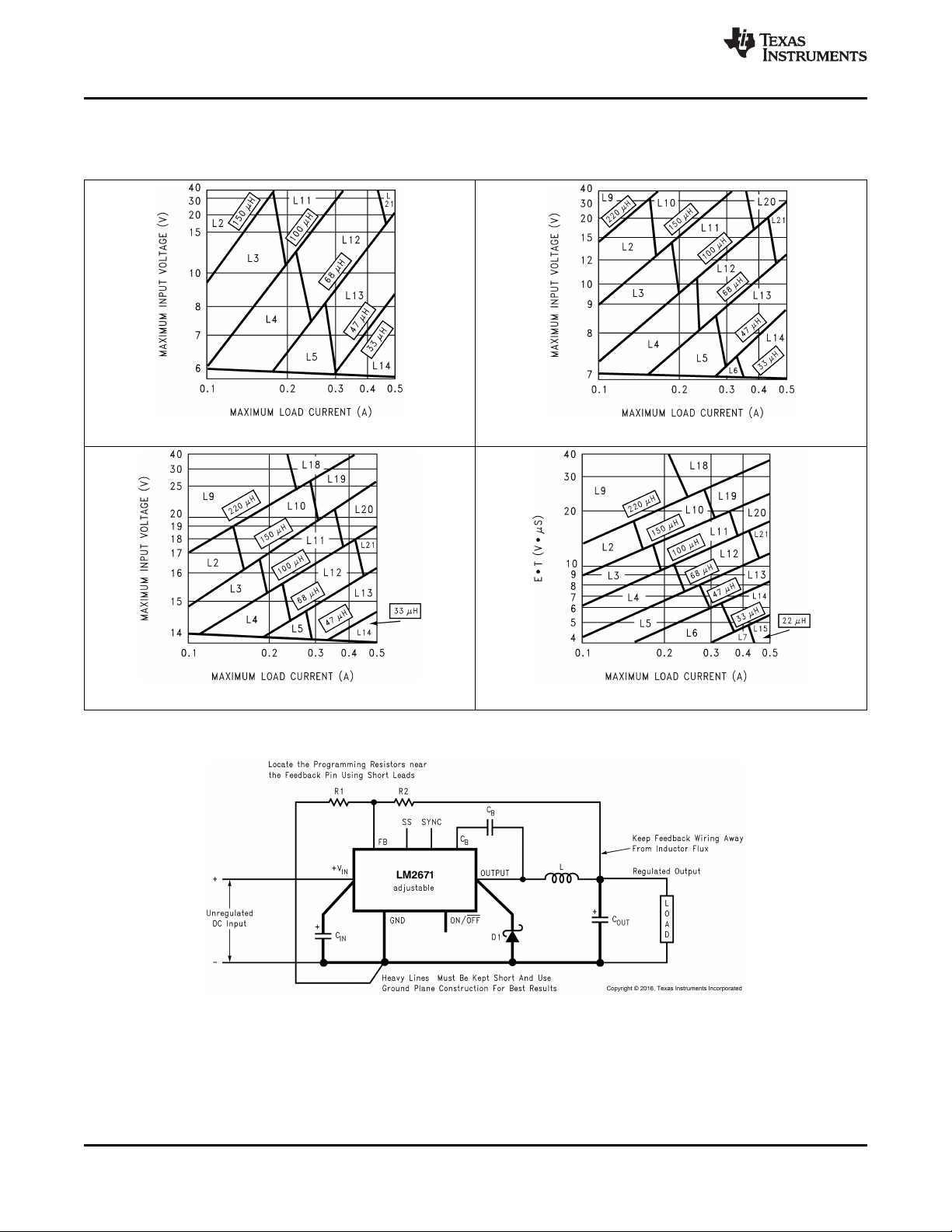
11 Layout
11.1 Layout Guidelines
Layout is very important in switching regulator designs. Rapidly switching currents associated with wiring
inductance can generate voltage transients which can cause problems. For minimal inductance and ground
loops, the wires indicated by heavy lines (in Figure 15 and Figure 21) must be wide printed-circuit traces and
must be kept as short as possible. For best results, external components must be placed as close to the switcher
IC as possible using ground plane construction or single point grounding.
If open core inductors are used, take special care as to the location and positioning of this type of inductor.
Allowing the inductor flux to intersect sensitive feedback, IC ground path, and C
When using the adjustable version, take special care as to the location of the feedback resistors and the
associated wiring. Physically place both resistors near the IC, and route the wiring away from the inductor,
especially an open core type of inductor.
11.2 Layout Examples
wiring can cause problems.
OUT
CIN= 15-μF, 25-V Solid Tantalum Sprague, 594D series
C
= 68-μF, 10-V Solid Tantalum Sprague, 594D series
OUT
D1 = 1-A, 40-V Schottky Rectifier, surface mount
L1 = 47-μH, L13 Coilcraft DO3308
CB= 0.01-μF, 50-V ceramic
Figure 27. Typical Surface Mount PCB Layout, Fixed Output (4x Size)
CIN= 15 μF, 50 V Solid Tantalum Sprague, 594D series
C
= 33 μF, 25 V Solid Tantalum Sprague, 594D series
OUT
D1 = 1-A, 40-V Schottky Rectifier, surface mount
L1 = 100-μH, L20 Coilcraft DO3316
CB= 0.01-μF, 50-V ceramic
R1 = 1 kΩ, 1%
R2 = Use formula in Detailed Design Procedure
Figure 28. Typical Surface Mount PCB Layout, Adjustable Output (4x Size)
Product Folder Links: LM2671
Submit Documentation FeedbackCopyright © 1998–2016, Texas Instruments Incorporated
27
Page 28
LM2671
SNVS008L –SEPTEMBER 1998–REVISED JUNE 2016
www.ti.com
12 Device and Documentation Support
12.1 Documentation Support
12.1.1 Related Documentation
For related documentation see the following:
• AN-1187 Leadless Leadfram Package (LLP)
• LM2670 SIMPLE SWITCHER®High Efficiency 3A Step-Down Voltage Regulator with Sync
12.2 Receiving Notification of Documentation Updates
To receive notification of documentation updates, navigate to the device product folder on ti.com. In the upper
right corner, click on Alert me to register and receive a weekly digest of any product information that has
changed. For change details, review the revision history included in any revised document.
12.3 Community Resources
The following links connect to TI community resources. Linked contents are provided "AS IS" by the respective
contributors. They do not constitute TI specifications and do not necessarily reflect TI's views; see TI's Terms of
Use.
TI E2E™ Online Community TI's Engineer-to-Engineer (E2E) Community. Created to foster collaboration
among engineers. At e2e.ti.com, you can ask questions, share knowledge, explore ideas and help
solve problems with fellow engineers.
Design Support TI's Design Support Quickly find helpful E2E forums along with design support tools and
contact information for technical support.
12.4 Trademarks
E2E is a trademark of Texas Instruments.
SIMPLE SWITCHER, WEBENCH are registered trademarks of Texas Instruments.
All other trademarks are the property of their respective owners.
12.5 Electrostatic Discharge Caution
These devices have limited built-in ESD protection. The leads should be shorted together or the device placed in conductive foam
during storage or handling to prevent electrostatic damage to the MOS gates.
12.6 Glossary
SLYZ022 — TI Glossary.
This glossary lists and explains terms, acronyms, and definitions.
13 Mechanical, Packaging, and Orderable Information
The following pages include mechanical, packaging, and orderable information. This information is the most
current data available for the designated devices. This data is subject to change without notice and revision of
this document. For browser-based versions of this data sheet, refer to the left-hand navigation.
13.1 DAP (WSON Package)
The die attach pad (DAP) can and must be connected to the PCB Ground plane. For CAD and assembly
guidelines refer to AN-1187 Leadless Leadfram Package (LLP).
28
Submit Documentation Feedback Copyright © 1998–2016, Texas Instruments Incorporated
Product Folder Links: LM2671
Page 29

PACKAGE OPTION ADDENDUM
www.ti.com
PACKAGING INFORMATION
Orderable Device Status
LM2671LD-ADJ NRND WSON NHN 16 1000 Non-RoHS
LM2671LD-ADJ/NOPB ACTIVE WSON NHN 16 1000 RoHS & Green SN Level-3-260C-168 HR -40 to 125 S0008B
LM2671M-12/NOPB ACTIVE SOIC D 8 95 RoHS & Green SN Level-1-260C-UNLIM -40 to 125 2671
LM2671M-3.3/NOPB ACTIVE SOIC D 8 95 RoHS & Green SN Level-1-260C-UNLIM -40 to 125 2671
LM2671M-5.0 NRND SOIC D 8 95 Non-RoHS
LM2671M-5.0/NOPB ACTIVE SOIC D 8 95 RoHS & Green SN Level-1-260C-UNLIM -40 to 125 2671
LM2671M-ADJ NRND SOIC D 8 95 Non-RoHS
LM2671M-ADJ/NOPB ACTIVE SOIC D 8 95 RoHS & Green SN Level-1-260C-UNLIM -40 to 125 2671
LM2671MX-12/NOPB ACTIVE SOIC D 8 2500 RoHS & Green SN Level-1-260C-UNLIM -40 to 125 2671
LM2671MX-3.3/NOPB ACTIVE SOIC D 8 2500 RoHS & Green SN Level-1-260C-UNLIM -40 to 125 2671
LM2671MX-5.0/NOPB ACTIVE SOIC D 8 2500 RoHS & Green SN Level-1-260C-UNLIM -40 to 125 2671
LM2671MX-ADJ/NOPB ACTIVE SOIC D 8 2500 RoHS & Green SN Level-1-260C-UNLIM -40 to 125 2671
LM2671N-12/NOPB ACTIVE PDIP P 8 40 RoHS & Green Call TI | SN Level-1-NA-UNLIM -40 to 125 LM2671
LM2671N-3.3/NOPB ACTIVE PDIP P 8 40 RoHS & Green Call TI | SN Level-1-NA-UNLIM -40 to 125 LM2671
LM2671N-5.0/NOPB ACTIVE PDIP P 8 40 RoHS & Green SN Level-1-NA-UNLIM -40 to 125 LM2671
LM2671N-ADJ/NOPB ACTIVE PDIP P 8 40 RoHS & Green SN Level-1-NA-UNLIM -40 to 125 LM2671
(1)
The marketing status values are defined as follows:
Package Type Package
(1)
Drawing
Pins Package
Qty
Eco Plan
(2)
& Green
& Green
& Green
Lead finish/
Ball material
(6)
MSL Peak Temp
(3)
Op Temp (°C) Device Marking
Call TI Call TI -40 to 125 S0008B
Call TI Call TI -40 to 125 2671
Call TI Call TI -40 to 125 2671
11-Jan-2021
Samples
(4/5)
M-12
M3.3
M5.0
M5.0
MADJ
MADJ
M-12
M3.3
M5.0
MADJ
N-12
N-3.3
N-5.0
N-ADJ
Addendum-Page 1
Page 30

PACKAGE OPTION ADDENDUM
www.ti.com
ACTIVE: Product device recommended for new designs.
LIFEBUY: TI has announced that the device will be discontinued, and a lifetime-buy period is in effect.
NRND: Not recommended for new designs. Device is in production to support existing customers, but TI does not recommend using this part in a new design.
PREVIEW: Device has been announced but is not in production. Samples may or may not be available.
OBSOLETE: TI has discontinued the production of the device.
11-Jan-2021
(2)
RoHS: TI defines "RoHS" to mean semiconductor products that are compliant with the current EU RoHS requirements for all 10 RoHS substances, including the requirement that RoHS substance
do not exceed 0.1% by weight in homogeneous materials. Where designed to be soldered at high temperatures, "RoHS" products are suitable for use in specified lead-free processes. TI may
reference these types of products as "Pb-Free".
RoHS Exempt: TI defines "RoHS Exempt" to mean products that contain lead but are compliant with EU RoHS pursuant to a specific EU RoHS exemption.
Green: TI defines "Green" to mean the content of Chlorine (Cl) and Bromine (Br) based flame retardants meet JS709B low halogen requirements of <=1000ppm threshold. Antimony trioxide based
flame retardants must also meet the <=1000ppm threshold requirement.
(3)
MSL, Peak Temp. - The Moisture Sensitivity Level rating according to the JEDEC industry standard classifications, and peak solder temperature.
(4)
There may be additional marking, which relates to the logo, the lot trace code information, or the environmental category on the device.
(5)
Multiple Device Markings will be inside parentheses. Only one Device Marking contained in parentheses and separated by a "~" will appear on a device. If a line is indented then it is a continuation
of the previous line and the two combined represent the entire Device Marking for that device.
(6)
Lead finish/Ball material - Orderable Devices may have multiple material finish options. Finish options are separated by a vertical ruled line. Lead finish/Ball material values may wrap to two
lines if the finish value exceeds the maximum column width.
Important Information and Disclaimer:The information provided on this page represents TI's knowledge and belief as of the date that it is provided. TI bases its knowledge and belief on information
provided by third parties, and makes no representation or warranty as to the accuracy of such information. Efforts are underway to better integrate information from third parties. TI has taken and
continues to take reasonable steps to provide representative and accurate information but may not have conducted destructive testing or chemical analysis on incoming materials and chemicals.
TI and TI suppliers consider certain information to be proprietary, and thus CAS numbers and other limited information may not be available for release.
In no event shall TI's liability arising out of such information exceed the total purchase price of the TI part(s) at issue in this document sold by TI to Customer on an annual basis.
Addendum-Page 2
Page 31

PACKAGE MATERIALS INFORMATION
www.ti.com 29-Sep-2019
TAPE AND REEL INFORMATION
*All dimensions are nominal
Device Package
LM2671LD-ADJ WSON NHN 16 1000 178.0 12.4 5.3 5.3 1.3 8.0 12.0 Q1
LM2671LD-ADJ/NOPB WSON NHN 16 1000 178.0 12.4 5.3 5.3 1.3 8.0 12.0 Q1
LM2671MX-12/NOPB SOIC D 8 2500 330.0 12.4 6.5 5.4 2.0 8.0 12.0 Q1
LM2671MX-3.3/NOPB SOIC D 8 2500 330.0 12.4 6.5 5.4 2.0 8.0 12.0 Q1
LM2671MX-5.0/NOPB SOIC D 8 2500 330.0 12.4 6.5 5.4 2.0 8.0 12.0 Q1
LM2671MX-ADJ/NOPB SOIC D 8 2500 330.0 12.4 6.5 5.4 2.0 8.0 12.0 Q1
Type
Package
Drawing
Pins SPQ Reel
Diameter
(mm)
Reel
Width
W1 (mm)
A0
(mm)B0(mm)K0(mm)P1(mm)W(mm)
Quadrant
Pin1
Pack Materials-Page 1
Page 32
PACKAGE MATERIALS INFORMATION
www.ti.com 29-Sep-2019
*All dimensions are nominal
Device Package Type Package Drawing Pins SPQ Length (mm) Width (mm) Height (mm)
LM2671LD-ADJ WSON NHN 16 1000 210.0 185.0 35.0
LM2671LD-ADJ/NOPB WSON NHN 16 1000 210.0 185.0 35.0
LM2671MX-12/NOPB SOIC D 8 2500 367.0 367.0 35.0
LM2671MX-3.3/NOPB SOIC D 8 2500 367.0 367.0 35.0
LM2671MX-5.0/NOPB SOIC D 8 2500 367.0 367.0 35.0
LM2671MX-ADJ/NOPB SOIC D 8 2500 367.0 367.0 35.0
Pack Materials-Page 2
Page 33

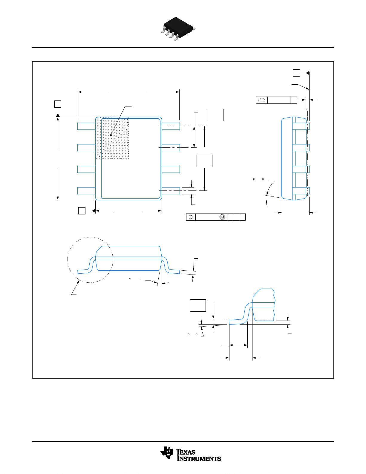
NHN0016A
MECHANICAL DATA
www.ti.com
LDA16A (REV A)
Page 34
PACKAGE OUTLINE
A
.189-.197
[4.81-5.00]
NOTE 3
.228-.244 TYP
[5.80-6.19]
1
4
B .150-.157
[3.81-3.98]
PIN 1 ID AREA
NOTE 4
SCALE 2.800
6X .050
[1.27]
8
2X
.150
[3.81]
5
8X .012-.020
[0.31-0.51]
.010 [0.25] C A B
SOIC - 1.75 mm max heightD0008A
SMALL OUTLINE INTEGRATED CIRCUIT
C
SEATING PLANE
.004 [0.1] C
4X (0 -15 )
.069 MAX
[1.75]
.005-.010 TYP
[0.13-0.25]
4X (0 -15 )
SEE DETAIL A
.010
[0.25]
0 - 8
.016-.050
[0.41-1.27]
(.041)
[1.04]
DETAIL A
TYPICAL
.004-.010
[0.11-0.25]
4214825/C 02/2019
NOTES:
1. Linear dimensions are in inches [millimeters]. Dimensions in parenthesis are for reference only. Controlling dimensions are in inches.
Dimensioning and tolerancing per ASME Y14.5M.
2. This drawing is subject to change without notice.
3. This dimension does not include mold flash, protrusions, or gate burrs. Mold flash, protrusions, or gate burrs shall not
exceed .006 [0.15] per side.
4. This dimension does not include interlead flash.
5. Reference JEDEC registration MS-012, variation AA.
www.ti.com
Page 35
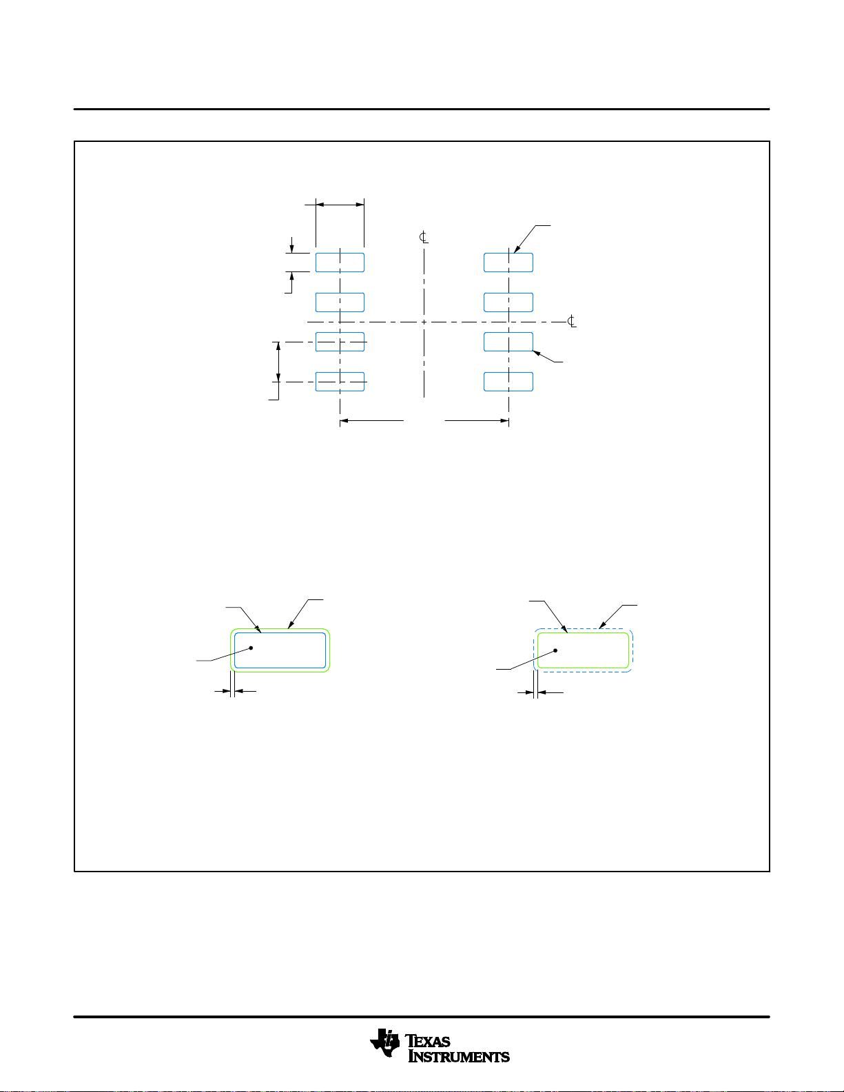
8X (.061 )
8X (.024)
6X (.050 )
[1.27]
[0.6]
[1.55]
SYMM
1
4
(.213)
[5.4]
LAND PATTERN EXAMPLE
EXPOSED METAL SHOWN
SCALE:8X
EXAMPLE BOARD LAYOUT
SOIC - 1.75 mm max heightD0008A
SMALL OUTLINE INTEGRATED CIRCUIT
SEE
DETAILS
8
SYMM
(R.002 ) TYP
5
[0.05]
EXPOSED
METAL
METAL
NON SOLDER MASK
SOLDER MASK
OPENING
.0028 MAX
[0.07]
ALL AROUND
DEFINED
SOLDER MASK
OPENING
EXPOSED
METAL
.0028 MIN
[0.07]
ALL AROUND
SOLDER MASK
DEFINED
SOLDER MASK DETAILS
NOTES: (continued)
6. Publication IPC-7351 may have alternate designs.
7. Solder mask tolerances between and around signal pads can vary based on board fabrication site.
METAL UNDER
SOLDER MASK
4214825/C 02/2019
www.ti.com
Page 36

8X (.061 )
8X (.024)
[0.6]
6X (.050 )
[1.27]
[1.55]
EXAMPLE STENCIL DESIGN
SOIC - 1.75 mm max heightD0008A
SMALL OUTLINE INTEGRATED CIRCUIT
SYMM
1
8
SYMM
(R.002 ) TYP
4
(.213)
[5.4]
5
[0.05]
BASED ON .005 INCH [0.125 MM] THICK STENCIL
NOTES: (continued)
8. Laser cutting apertures with trapezoidal walls and rounded corners may offer better paste release. IPC-7525 may have alternate
design recommendations.
9. Board assembly site may have different recommendations for stencil design.
SCALE:8X
4214825/C 02/2019
SOLDER PASTE EXAMPLE
www.ti.com
Page 37
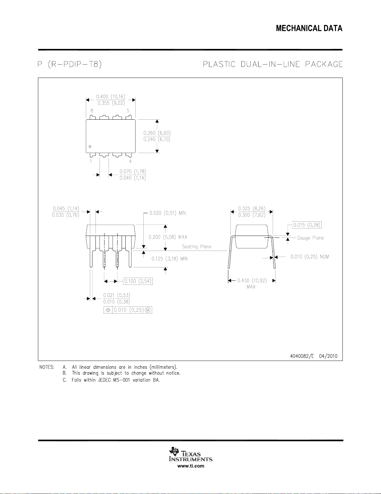
Page 38

IMPORTANT NOTICE AND DISCLAIMER
TI PROVIDES TECHNICAL AND RELIABILITY DATA (INCLUDING DATASHEETS), DESIGN RESOURCES (INCLUDING REFERENCE
DESIGNS), APPLICATION OR OTHER DESIGN ADVICE, WEB TOOLS, SAFETY INFORMATION, AND OTHER RESOURCES “AS IS”
AND WITH ALL FAULTS, AND DISCLAIMS ALL WARRANTIES, EXPRESS AND IMPLIED, INCLUDING WITHOUT LIMITATION ANY
IMPLIED WARRANTIES OF MERCHANTABILITY, FITNESS FOR A PARTICULAR PURPOSE OR NON-INFRINGEMENT OF THIRD
PARTY INTELLECTUAL PROPERTY RIGHTS.
These resources are intended for skilled developers designing with TI products. You are solely responsible for (1) selecting the appropriate
TI products for your application, (2) designing, validating and testing your application, and (3) ensuring your application meets applicable
standards, and any other safety, security, or other requirements. These resources are subject to change without notice. TI grants you
permission to use these resources only for development of an application that uses the TI products described in the resource. Other
reproduction and display of these resources is prohibited. No license is granted to any other TI intellectual property right or to any third party
intellectual property right. TI disclaims responsibility for, and you will fully indemnify TI and its representatives against, any claims, damages,
costs, losses, and liabilities arising out of your use of these resources.
TI’s products are provided subject to TI’s Terms of Sale (https:www.ti.com/legal/termsofsale.html) or other applicable terms available either
on ti.com or provided in conjunction with such TI products. TI’s provision of these resources does not expand or otherwise alter TI’s
applicable warranties or warranty disclaimers for TI products.IMPORTANT NOTICE
Mailing Address: Texas Instruments, Post Office Box 655303, Dallas, Texas 75265
Copyright © 2021, Texas Instruments Incorporated
 Loading...