

Page 1

1 Introduction
The LM267X evaluation board was developed for the evaluation of LM267X SIMPLE SWITCHER series of
3 Amp and 5 Amp high efficiency step-down (Buck) switching voltage regulators. This application note
describes the printed circuit board, and provides example circuits and directions on setup and operation of
the LM2673S-5_EVAL and LM2679S-5_EVAL evaluation boards.
2 General Description
Many of our boards are intended to provide the user with device characterization and layout optimization
data. The LM267x evaluation board was intended to allow the user to experiment with a variety of circuit
topologies and components, and therefore not optimized for size. Please refer to the discussions of layout
optimization in the PCB Layout Optimization section.
This board was designed such that both through-hole and surface-mount components can be used for
construction. The regulator IC can be placed on the board as a surface-mount component only. The
ground plane serves as a heatsink.
Table 1 shows an overview of the family of devices with special features of each indicated. Consult the
device data sheet, or use the special power supply design software calledSwitchers Made Simple
version 6.X (available for free download from www.ti.com) to determine all necessary component values
for the particular device being used to accomplish a specific design and board layout considerations.
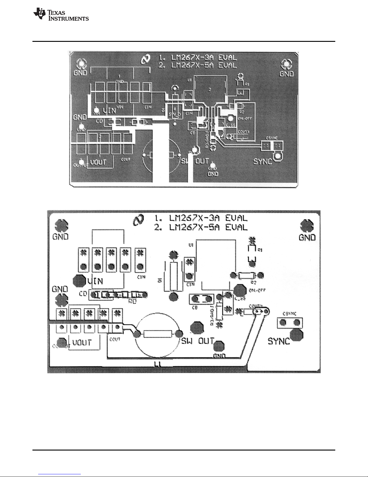
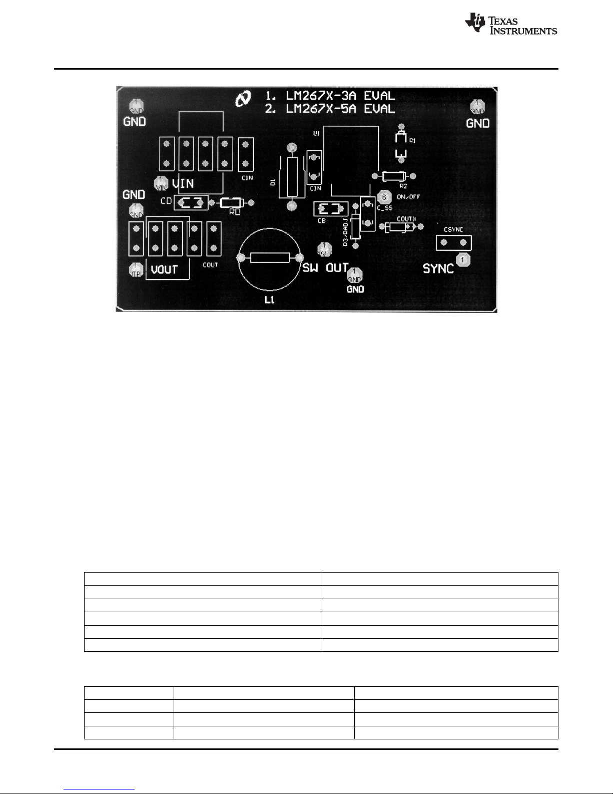
The printed circuit board, PCB, is labeled to indicate the location of all of the needed components for all
possible design options. Table 2 shows a complete list of the component labels and their functions.
Figure 1 identifies all components, but not all are necessary in every design.
Figure 2, Figure 3 and Figure 4 show the top, bottom and silk screen of the printed circuit board
respectively.
User's Guide
SNVA013D–December 2000–Revised April 2013
AN-1135 LM267X 3A, 5A Evaluation Boards
Table 1. LM267X Family of High-Current Regulators supported by the Evaluation Board
Device Maximum Load Current (A) Special Features
LM2670 3 ON/OFF, External Frequency Sync Capability
LM2673 3 Adjustable Current Limit, Softstart
LM2676 3 ON/OFF
LM2677 5 ON/OFF, External Frequncy Sync. Capability
LM2678 5 ON/OFF
LM2679 5 Adjustable Current Limit, Softstart
SNVA013D–December 2000–Revised April 2013 AN-1135 LM267X 3A, 5A Evaluation Boards
Submit Documentation Feedback
1
Copyright © 2000–2013, Texas Instruments Incorporated
Page 2

General Description
www.ti.com
Figure 1. Example Schematic Showing Connection for all Components.
Table 2. List of Component Labels and Functionality
Label Function
U1 LM267 Switching Regulator IC
CIN Input Capacitor(s); All devices.
CINX 0.47 µF, optional high frequency input bypass capacitor, recommended in all designs: All
devices.
CB Boost capacitor; All devices.
D1 Catch diode; All devices.
R1 Feedback resistor for adjustable output converters. This designator is left open (not
connected) for fixed output converters.
R2 Feedback resistor (typ. 1 kΩ) for adjustable output converters. This designator is left shorted
(replaced by a jumper wire) for fixed output voltage converters.
R3* Current limit resistor for LM2673, LM2679; Sync input resistor (1 kΩ) for LM2670 and
LM2677; Not inserted for LM2676 and LM2678.
L1 Inductor; All devices.
CSYNC Sync input capacitor (100 pF); LM2670 and LM2677only. Not inserted with other devices.
CSS Soft start capacitor; LM2673 and LM2679 only. Not inserted with other devices.
COUTX 0.47 µF, optional high frequency output bypass capacitor; All devices.
COUT Output capacitor(s); All devices.
2
AN-1135 LM267X 3A, 5A Evaluation Boards SNVA013D–December 2000–Revised April 2013
Copyright © 2000–2013, Texas Instruments Incorporated
Submit Documentation Feedback
Page 3
www.ti.com
General Description
Figure 2. Top Layer Foil Pattern of Printed Circuit Board
Figure 3. Bottom Layer Foil Pattern of Printed Circuit Board
SNVA013D–December 2000–Revised April 2013 AN-1135 LM267X 3A, 5A Evaluation Boards
Submit Documentation Feedback
3
Copyright © 2000–2013, Texas Instruments Incorporated
Page 4
Special Notes
www.ti.com
Figure 4. Silkscreen Image of Printed Circuit Board
3 Special Notes
The evaluation board was designed primarily for circuit implementation using all surface-mount
components. The small series "trace inductance", particularly from the Switch Output pin, can create a
high frequency (10's of MHz) ringing signal at the switch output. If problematic, this ringing can be reduced
or eliminated by the use of a series RC damper or snubber network from the switch output to ground. The
addition of these components is made at the locations labeled CD and RD. Values of 0.01 µF and 10Ω are
good starting values that may need to be varied depending on the magnitude of parasitic factors in a given
design. In an actual end application, these components are normally not required if proper care to
minimize trace lengths is taken in the PCB design.
4 Example Circuit Designs
Example 1: 5V/3A Converter with Surface Mount Components.
In this example, it is desired to convert a voltage range of between 8V and 12V, to 5VDC with load current
of 3A. It is also desired to implement the design with surface mount components only. Softstart duration
will be set to between 1 and 1.5 ms.
VINmin. 8V
VINmax. 16V
V
OUT
I
LOAD
I
CL
T
SS
Table 3. Target Design Specifications
5V
3A
5.0A (approx.)
1 to 1.5 ms
Table 4. Component Values for an 8-12V in, 5V/3A Out LM2673S-5.0 Buck Converter
Component Value Suggested Part Number
U1 Texas Instruments LM2673
CIN 2 x 33 µF/35V Vishay 594D336X0035R2T
CINX 0.47 µF Vishay VJ1210U474ZXAA
4
AN-1135 LM267X 3A, 5A Evaluation Boards SNVA013D–December 2000–Revised April 2013
Submit Documentation Feedback
Copyright © 2000–2013, Texas Instruments Incorporated
Page 5

www.ti.com
Figure 5 below shows the 5V/3A design circuit. This solution is available as evaluation board LM2673S-
5_EVAL.
Figure 6 through Figure 9 show the output waveforms for output voltage with 500 mA load, output voltage
with 1A load, output ripple with 1A load, output voltage with 3A load, output ripple with 3A load, output
response to 1A transient load and output response to 3A transient load respectively.
Example Circuit Designs
Table 4. Component Values for an 8-12V in, 5V/3A Out LM2673S-5.0 Buck Converter (continued)
Component Value Suggested Part Number
CB 0.01 µF/50V Vishay VJ1206Y103MXXA
D1 3A/60V Schottky (450 mV at 3A) Motorola MBRD360
R3* 7.15 kΩ Vishay CRCW12067151J
(5.19A current limit)
L1 22 µH (L41) SUMIDA ELECTRIC CO. CDRH127-220
CSS 3.3 nF/100V (softstart) Vishay VJ1206Y33ZJXBAB
COUTX 0.47 µF Vishay VJ1210U474ZXAA
COUT 2 x 18 0µF/16V Vishay 594D187X0016R2T
A: OUTPUT VOLTAGE: V
B: LOAD CURRENT: I
LOAD
Figure 5. 5V/3A Design Circuit
; 2V/DIV
OUT
= 500 mA; 500 mA/DIV
Figure 6. Output Voltage with 500 mA Load
SNVA013D–December 2000–Revised April 2013 AN-1135 LM267X 3A, 5A Evaluation Boards
Submit Documentation Feedback
5
Copyright © 2000–2013, Texas Instruments Incorporated
Page 6

Example Circuit Designs
A: OUTPUT RIPPLE; 10 mV/DIV
B: LOAD CURRENT: I
= 0.5A; 1A/DIV
LOAD
www.ti.com
Figure 7. Output Ripple with 500 mA Load
A: OUTPUT VOLTAGE: V
B: LOAD CURRENT: I
; 2V/DIV
OUT
= 1A; 500 mA/DIV
LOAD
A: OUTPUT RIPPLE; 10 mV/DIV
B: LOAD CURRENT: I
= 1A; 1A/DIV
LOAD
Figure 8. Output Voltage with 1A Load
Figure 9. Output Ripple with 1 Amp Load
6
AN-1135 LM267X 3A, 5A Evaluation Boards SNVA013D–December 2000–Revised April 2013
Copyright © 2000–2013, Texas Instruments Incorporated
Submit Documentation Feedback
Page 7

www.ti.com
Example Circuit Designs
A: OUTPUT VOLTAGE: V
B: LOAD CURRENT: I
OUT
= 3A; 1A/DIV
LOAD
; 2V/DIV
A: OUTPUT RIPPLE; 10 mV/DIV
B: LOAD CURRENT: I
= 3A; 1A/DIV
LOAD
Figure 10. Output Voltage with 3A Load
Figure 11. Output Ripple with 3 Amp Load
A: OUTPUT RESPONSE; 1V/DIV
B: TRANSIENT LOAD CURRENT: 1A/DIV
Figure 12. Output Response to 0∼∼1A Transient Load
SNVA013D–December 2000–Revised April 2013 AN-1135 LM267X 3A, 5A Evaluation Boards
Submit Documentation Feedback
7
Copyright © 2000–2013, Texas Instruments Incorporated
Page 8

Example 2: 5V/5A Design with Surface Mount Components
A: OUTPUT RESPONSE; 1V/DIV
B: TRANSIENT LOAD CURRENT: 2A/DIV
Figure 13. Output Response to 0∼∼3A Load Transient
5 Example 2: 5V/5A Design with Surface Mount Components
For this example, it is desired to design a power supply to convert an input voltage within the range of 14V
and 28V to an output voltage of 5V with a maximum load current of 5A using only surface mount
components. In addition, the current limit of the regulator will be set to approximately 7.0A, and the
softstart time will be set to approximately 1.0 ms to limit the startup surge current.
www.ti.com
Table 5. Target Design Specifications:
VINmin. 14V
VINmax. 28V
V
I
LOAD
T
I
OUT
CL
SS
5V
5A
7.0A (approx.)
1.0 ms (approx.)
Table 6. Component Values for an 14V-28V in, 5V/5A Out LM2679S-5.0 Buck Converter
Component Value Suggested Part Number
U1 Texas Instruments LM2679
CIN 3 x 15 µF/50V Vishay 594D156X0050R2T
CINX 0.47µF Vishay VJ1210U474ZXAA
CB 0.01µF/50V Vishay VJ1206Y103ZXXA
D1 8A/35V Schottky (500 mV at 5A) Motorola MBRD835L
R3* 4.99 kΩ (7.19A current limit) Vishay CRCW12064991J
L1 15 µH Coilcraft D05022P-153
CSS 4.7 nF/100V (1.0 ms softstart) Vishay VJ1206Y47ZJXBAB
COUTX 0.47 µF Vishay VJ1210U474ZXAA
COUT 2 x 180 µF/16V Vishay 594D187X0016R2T
Figure 14 below shows the circuit for the 5V/5A design. This solution is available as evaluation board
LM2679S-5_EVAL.
Figure 14 through Figure 23 show the output waveforms for output voltage with 500 mA load, output
voltage with 2.5A load, output ripple with 2.5A load, output voltage with 5A load, output ripple with 5A
load, output response to 500 mA transient load, output response to 2.5A transient load and output
response to 5A transient load respectively.
8
AN-1135 LM267X 3A, 5A Evaluation Boards SNVA013D–December 2000–Revised April 2013
Copyright © 2000–2013, Texas Instruments Incorporated
Submit Documentation Feedback
Page 9

www.ti.com
Example 2: 5V/5A Design with Surface Mount Components
Figure 14. 5V/5A Design Circuit
A: OUTPUT VOLTAGE: V
B: LOAD CURRENT: I
; 2V/DIV
OUT
= 500 mA; 500 mA/DIV
LOAD
Figure 15. Output Voltage with 500 mA Load
A: OUTPUT RIPPLE; 100 mV/DIV
B: LOAD CURRENT: I
= 500 mA; 1A/DIV
LOAD
Figure 16. Output Ripple with 500 mA Load
SNVA013D–December 2000–Revised April 2013 AN-1135 LM267X 3A, 5A Evaluation Boards
Submit Documentation Feedback
9
Copyright © 2000–2013, Texas Instruments Incorporated
Page 10

Example 2: 5V/5A Design with Surface Mount Components
www.ti.com
A: OUTPUT VOLTAGE: V
B: LOAD CURRENT: I
; 2V/DIV
OUT
= 2.5A; 1A/DIV
LOAD
Figure 17. Output Voltage with 2.5A Load
A: OUTPUT RIPPLE; 100 mV/DIV
B: LOAD CURRENT: I
= 2.5A; 2A/DIV
LOAD
Figure 18. Output Ripple with 2.5A Load
10
A: OUTPUT VOLTAGE: V
B: LOAD CURRENT: I
AN-1135 LM267X 3A, 5A Evaluation Boards SNVA013D–December 2000–Revised April 2013
OUT
= 5A; 2A/DIV
LOAD
; 2V/DIV
Figure 19. Output Voltage with 5A Load
Copyright © 2000–2013, Texas Instruments Incorporated
Submit Documentation Feedback
Page 11

www.ti.com
A: OUTPUT RIPPLE; 100 mV/DIV
B: LOAD CURRENT: I
= 5A; 5A/DIV
LOAD
Example 2: 5V/5A Design with Surface Mount Components
Figure 20. Output Ripple with 5A Load
A: OUTPUT RESPONSE; 1V/DIV
B: TRANSIENT LOAD CURRENT: 500 mA/DIV
Figure 21. Output Response to 0∼∼0.5A Transient Load
A: OUTPUT RESPONSE; 1V/DIV
B: TRANSIENT LOAD CURRENT: 1A/DIV
Figure 22. Output Response to 0∼∼2.5A Load Transient
SNVA013D–December 2000–Revised April 2013 AN-1135 LM267X 3A, 5A Evaluation Boards
Submit Documentation Feedback
11
Copyright © 2000–2013, Texas Instruments Incorporated
Page 12
Operating the Evaluation Boards
A: OUTPUT RESPONSE: 1V/DIV
B: LOAD CURRENT: I
LOAD
= 1A/DIV
Figure 23. Output Response to 0∼∼5A Transient Load
6 Operating the Evaluation Boards
6.1 Setup
The LM2673S-5_EVAL and LM2679S-5_EVAL evaluation boards come ready to be tested. The only
setup needed is connecting the input voltage to the VIN and GND posts. The output can be taken from the
VOUT post. The other signals of interest, switch output (SW out) and softstart (C_SS) posts, are clearly
marked for use in checking the signal integrity. The softstart post has an ON/OFF input when this feature
is being used.
www.ti.com
6.2 Operating Conditions
The input source for the LM267x family of regulators must be 8V or greater for proper setup and
operation. The input voltage range for LM2673S-5_EVAL evaluation board is from 8V to 12V and the
range for LM2679S-5_EVAL is from 14V to 28V. The maximum voltage rating of the LM267x family of
regulators is 40V.
Load can be applied from 0A to the maximum for the design. Higher current above the design current limit
will result in activation of the design current limit circuit. It is advisable to have a minimal load of (at least
10 mA) during startup when the input to output differential voltage is greater than 10V to prevent output
ramping beyond desired value.
6.3 PCB Layout Optimization
As in any switching regulator, layout is very important. Rapidly switching currents associated with wiring
inductance can generate voltage transients which can cause problems. For minimal inductance and
ground loops, the printed circuit traces should be as wide and short as possible on the PCB. For best
results, external components should be located as close to the switcher IC as possible using ground plane
construction or single point grounding.
If open core inductors are used, special care must be taken as to the location and positioning of this
type of inductor. Allowing the inductor flux to intersect sensitive feedback, IC groundpath and C
can cause problems.
When using the adjustable version, special care must be taken as to the location of the feedback resistors
and associated wiring. Physically locate both resistors near the IC, and route the wiring away from the
inductor, especially an open core type of inductor.
OUT
wiring
12
AN-1135 LM267X 3A, 5A Evaluation Boards SNVA013D–December 2000–Revised April 2013
Copyright © 2000–2013, Texas Instruments Incorporated
Submit Documentation Feedback
Page 13

IMPORTANT NOTICE
Texas Instruments Incorporated and its subsidiaries (TI) reserve the right to make corrections, enhancements, improvements and other
changes to its semiconductor products and services per JESD46, latest issue, and to discontinue any product or service per JESD48, latest
issue. Buyers should obtain the latest relevant information before placing orders and should verify that such information is current and
complete. All semiconductor products (also referred to herein as “components”) are sold subject to TI’s terms and conditions of sale
supplied at the time of order acknowledgment.
TI warrants performance of its components to the specifications applicable at the time of sale, in accordance with the warranty in TI’s terms
and conditions of sale of semiconductor products. Testing and other quality control techniques are used to the extent TI deems necessary
to support this warranty. Except where mandated by applicable law, testing of all parameters of each component is not necessarily
performed.
TI assumes no liability for applications assistance or the design of Buyers’ products. Buyers are responsible for their products and
applications using TI components. To minimize the risks associated with Buyers’ products and applications, Buyers should provide
adequate design and operating safeguards.
TI does not warrant or represent that any license, either express or implied, is granted under any patent right, copyright, mask work right, or
other intellectual property right relating to any combination, machine, or process in which TI components or services are used. Information
published by TI regarding third-party products or services does not constitute a license to use such products or services or a warranty or
endorsement thereof. Use of such information may require a license from a third party under the patents or other intellectual property of the
third party, or a license from TI under the patents or other intellectual property of TI.
Reproduction of significant portions of TI information in TI data books or data sheets is permissible only if reproduction is without alteration
and is accompanied by all associated warranties, conditions, limitations, and notices. TI is not responsible or liable for such altered
documentation. Information of third parties may be subject to additional restrictions.
Resale of TI components or services with statements different from or beyond the parameters stated by TI for that component or service
voids all express and any implied warranties for the associated TI component or service and is an unfair and deceptive business practice.
TI is not responsible or liable for any such statements.
Buyer acknowledges and agrees that it is solely responsible for compliance with all legal, regulatory and safety-related requirements
concerning its products, and any use of TI components in its applications, notwithstanding any applications-related information or support
that may be provided by TI. Buyer represents and agrees that it has all the necessary expertise to create and implement safeguards which
anticipate dangerous consequences of failures, monitor failures and their consequences, lessen the likelihood of failures that might cause
harm and take appropriate remedial actions. Buyer will fully indemnify TI and its representatives against any damages arising out of the use
of any TI components in safety-critical applications.
In some cases, TI components may be promoted specifically to facilitate safety-related applications. With such components, TI’s goal is to
help enable customers to design and create their own end-product solutions that meet applicable functional safety standards and
requirements. Nonetheless, such components are subject to these terms.
No TI components are authorized for use in FDA Class III (or similar life-critical medical equipment) unless authorized officers of the parties
have executed a special agreement specifically governing such use.
Only those TI components which TI has specifically designated as military grade or “enhanced plastic” are designed and intended for use in
military/aerospace applications or environments. Buyer acknowledges and agrees that any military or aerospace use of TI components
which have not been so designated is solely at the Buyer's risk, and that Buyer is solely responsible for compliance with all legal and
regulatory requirements in connection with such use.
TI has specifically designated certain components as meeting ISO/TS16949 requirements, mainly for automotive use. In any case of use of
non-designated products, TI will not be responsible for any failure to meet ISO/TS16949.
Products Applications
Audio www.ti.com/audio Automotive and Transportation www.ti.com/automotive
Amplifiers amplifier.ti.com Communications and Telecom www.ti.com/communications
Data Converters dataconverter.ti.com Computers and Peripherals www.ti.com/computers
DLP® Products www.dlp.com Consumer Electronics www.ti.com/consumer-apps
DSP dsp.ti.com Energy and Lighting www.ti.com/energy
Clocks and Timers www.ti.com/clocks Industrial www.ti.com/industrial
Interface interface.ti.com Medical www.ti.com/medical
Logic logic.ti.com Security www.ti.com/security
Power Mgmt power.ti.com Space, Avionics and Defense www.ti.com/space-avionics-defense
Microcontrollers microcontroller.ti.com Video and Imaging www.ti.com/video
RFID www.ti-rfid.com
OMAP Applications Processors www.ti.com/omap TI E2E Community e2e.ti.com
Wireless Connectivity www.ti.com/wirelessconnectivity
Mailing Address: Texas Instruments, Post Office Box 655303, Dallas, Texas 75265
Copyright © 2013, Texas Instruments Incorporated
Page 14

Mouser Electronics
Authorized Distributor
Click to View Pricing, Inventory, Delivery & Lifecycle Information:
Texas Instruments:
LM2673-5.0EVAL LM2679-5.0EVAL LM2679-5.0EVAL/NOPB
 Loading...