

Page 1

LM20125,LM26480,LM3743,LM3880,LMZ10504,
LMZ14203
????FPGA????????????????
Literature Number: ZHCA410
Page 2
POWER designer
Expert tips, tricks, and techniques for powerful designs
No. 121
national.com/powerdesigner
Power Supply Design Considerations for
Modern FPGAs
— By Dennis Hudgins, Low Voltage Applications Manages, Tucson Design Center
Introduction
Today’s FPGAs tend to operate at lower voltages and higher currents than their predecessors. Consequently,
power supply requirements may be more demanding, requiring special attention to features deemed less
important in past generations. Failure to consider the output voltage, sequencing, power-on, and soft-start
requirements can result in unreliable power-up or potential damage to FPGAs.
Output Voltage Requirements
e fi rst criteria to consider when designing power supplies for FPGAs are the voltage requirements for the
diff erent supply rails. Most FPGAs have specifi cations for the CORE and IO voltage rails and many require
additional auxiliary rails that may power internal clocks, phase-lock loops or transceivers. Table 1 provides
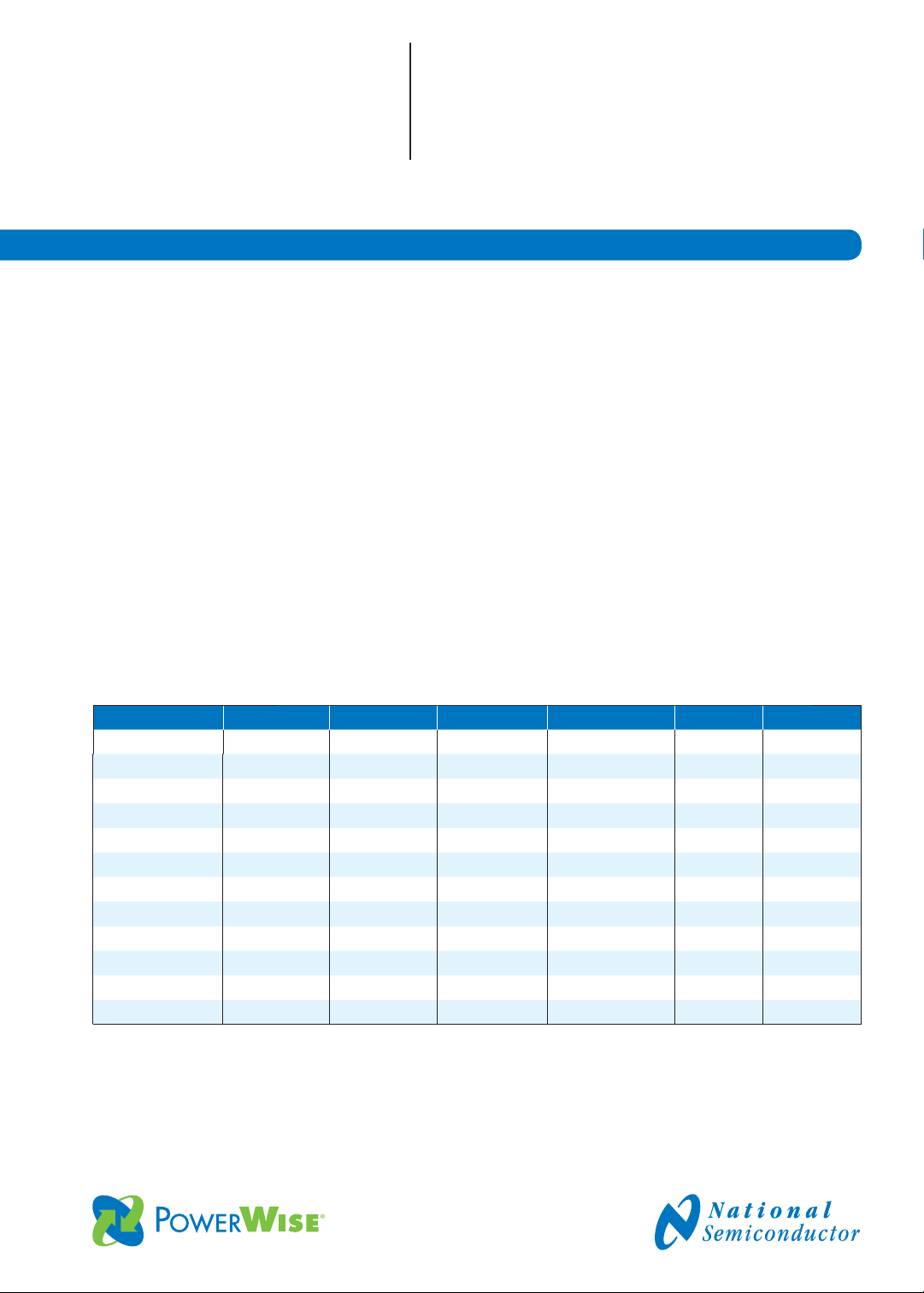
the voltage levels and tolerances for some of the newest FPGAs.
FPGA Core Core Tolerance Auxiliary Power Auxiliary Tolerance IO Voltage* IO Tolerance*
Spartan-6 1.2 5% 2.5 or 3.3 5% 1.2 to 3.3 1.1 to 3.45
Spartan-6 (-1L) 1.0 5% 2.5 or 3.3 5% 1.2 to 3.3 1.1 to 3.45
Virtex-6 1.0 5% 2.5 5% 1.2 to 2.5 1.14 to 2.625
Virtex-6 (-1L) 0.9 30 mV 2.5 5% 1.2 to 2.5 1.14 to 2.625
Stratix-IV (GX and E) 0.9 30 mV 2.5 (VCCA_PLL) 5% 1.2 to 3.0 5%
Stratix-IV (GT) 0.95 30 mV 2.5 (VCCA_PLL) 5% 1.2 to 3.0 5%
Cyclone-IV (GX) 1.2 40 mV 2.5 5% 1.2 to 3.3 5%
Cyclone-IV (E) 1.0 * 2.5 5% 1.2 to 3.3 5%
Arria-II 0.9 30 mV 2.5 (VCCA_PLL) 5% 1.2 to 3.3 5%
Table 1. Voltage Requirements for Common Modern FPGAs
0.90 (VCCD_PLL) 30 mV
0.95 (VCCD_PLL) 30 mV
0.90 (VCCD_PLL) 30 mV
* Some values may differ slightly from those listed. Please consult your FPGA’s associated documentation for details.
Page 3

POWER designer
Power Supply Design Considerations for Modern FPGAs
Since FPGAs generally specify several permissible
voltage levels for the IO, the voltage selected is dictated
by the external digital circuitry. To provide fl exibility,
FPGAs will generally provide multiple IO banks that
can be powered separately, allowing FPGAs to
interface with various logic families. For simplicity,
the solutions illustrated in this article will assume all
IO banks are powered off of a single power supply rail.
e core voltage supplies the internal logic
confi guration blocks of FPGAs and is where many of
the internal digital path processes occur. As such, the
current demanded by the core will vary greatly
depending on the percent utilization of FPGAs.
Vendors of the FPGAs described herein provide design
tools that estimate core current requirements based on
the internal blocks utilized.
Over time, the voltages used to power the core have
steadily dropped. Modern cores utilize 65 nm, 45 nm
or even 40 nm geometry silicon processes and may
operate from voltages as low as 0.9V. ese lower
voltages are valuable to reduce power dissipation in
FPGAs. e trade off , however, is that keeping within
the voltage tolerance requirements becomes more
challenging for the power supply designer.
Output Capacitance and Transient Considerations
A good power supply design will keep the core
voltage within tolerance at all times. Most of the
power supply transient concerns can be managed by
properly selecting the bypass and bulk capacitances for
the power supply. In general, every core ball or pin
connection should be bypassed directly under FPGAs
with high-quality X5R or X7R ceramic capacitors.
e values recommended for each of these capacitors
range from 1 μF to 10 μF and will generally be
specifi ed by FPGA manufacturers. ese capacitors
provide a charge when FPGAs need to rapidly draw
large spikes of current during high speed operations.
Likewise, the bulk capacitance should be selected to
provide charge during large steps of current, which
tend to occur during power-on, application-start,
or a change in application state. Before increasing
the amount of output capacitance to solve transient
droop issues, changes to the power supply should be
made that do not involve an increase in PCB area or
component count.
e response to a load transient is dictated by the
large signal response time that consists of ramping the
inductor current to the correct operating level and the
small signal response of the control loop.
Transient Response Optimizations
To optimize the transient response, ensure the supply
is switching at the highest possible frequency. is
will allow use of a small inductor and reduce the large
signal response time. Typical high performance power
supply solutions can be designed to have crossover
frequencies as high as one-tenth to one-fi fth the
switching frequency. Pushing the crossover frequency
too high may result in ringing at the output during
a load transient indicating poor phase margin. Any
ringing in the output should be avoided as this may
result in instability with external component variation
or when operating at temperature extremes.
AUX Voltage Considerations
Many FPGAs require a third power supply commonly
referred to as the auxiliary rail or AUX. Since the AUX
rail may power internal clocks, phase-lock loops, or
transceivers, the amount of output voltage ripple on
this rail should be minimized. In some cases, additional
ferrite beads and capacitors fi ltering may be needed to
meet the application or FPGA noise requirements. In
applications where noise is extremely important, a low
noise, high PSRR LDO, like the LP3878, should be
considered instead of a switching converter.
Sequencing Requirements
e sequencing requirements vary depending on
the particular FPGA being used and many newer
FPGAs specify that no sequencing is required. While
this is technically true for the FPGA, it is not the
optimal way to design a power solution. National
Semiconductor off ers several devices to address
sequencing requirements. e LM3880 is designed to
address sequential sequencing of multiple supply rails.
is device is available in a small SOT-23 package and
can sequence up to three supply rails. Many options
are available to control the up and down, three-fl ag
outputs sequencing timing. National also provides
devices to support customized fl ag order and timing.
2
Page 4

POWER designer
Figure 1 illustrates a typical application circuit for the
LM3880.
LM3880
FLAG1
V
IN
VIN
EN
GND
FLAG2
FLAG3
Power
Supply 1
EN
EN EN
Power
Supply 2
EN
Power
Supply 3
Figure 1. Simplifi ed Buck Converter Schematic
Voltage tracking is another method of sequencing
power supplies applicable to FPGAs and many
processors. e most common and generally
recommended method to power up FPGAs and other
processors is to have the CORE voltage track the I/O
voltage during startup as shown in Figure 2.
V
CORE
V
IO
Voltage
Time
V
ENABLE 1
Figure 2. Startup voltage tracking
is power-up technique is known as simultaneous
startup, and its primary advantage is that it avoids
turning on any parasitic conduction paths that may
exist between the CORE and IO supply rails. Turning
on a parasitic conduction path may lead to unreliable
startup or even damage to FPGAs or DSPs. Some
of National’s devices that feature voltage tracking
include the LMZ14203 and LMZ10504 SIMPLE
SWITCHER® Power Modules, the LM20k family of
high performance synchronous DC/DC converters, as
well as the LM3743 controller.
Figure 3 illustrates a typical voltage tracking
confi guration for these devices.
Master Supply
V
CORE
Tracking Supply
EN
R1
SS/TRK
R2
V
IO
Figure 3. Typical voltage tracking confi guration
Startup / Power-on Requirements
When sequential sequencing is used in systems with
multiple voltage rails, as is the case with many FPGA
solutions, it is likely that an output of one of the power
supplies could be pre-biased through various parasitic
conduction paths. In this situation, how the power
supply handles this pre-biased state can have an impact
on long term system reliability, or even the ability of
the power supply or FPGAs to start successfully. To
avoid the pitfalls associated with a pre-biased startup,
the power supply should not pull the output low if
a pre-biased condition exists. Figure 4 illustrates how
a pre-biased condition should be handled when the
output is pre-biased to three diff erent voltage levels.
All power solutions featured in this publication are
capable of properly handling a pre-biased start up.
Power supplies used to power both the CORE and IO
must be monotonic during power-on to avoid FPGA
startup problems. A monotonic startup continuously
increases until the output reaches the fi nal value.
V
OUT3
V
V
OUT2
OUT2
500 mV/DIV
national.com/powerdesigner
2 ms/DIV
Figure 4. Pre-biased startup of the LM3743
3
Page 5

POWER designer
Power Supply Design Considerations for Modern FPGAs
e critical area for monitonicity for most modern
core voltage rails occurs between 0.5V to 0.9V. is
is when FPGAs initialize the internal logic blocks to
valid operating states.
Soft-start Requirements
Using soft-start is highly recommended, even if not
specifi ed by the FPGA manufacturer. Slowly ramping
the input voltage reduces the inrush currents seen in
some FPGAs. Using soft-start also reduces the current
needed to charge the output capacitance of the power
supply and will decrease the voltage droop on the
input bus during startup.
e startup or soft-start requirements for several
FPGAs are summarized in Table 2.
Table 2. Required Startup/Soft-start Times
FPGA Min Max
Spartan-6
(-3 & -2 Speeds) 0.20 ms 50 ms
Spartan-6
(-1L speed grade) 0.20 ms 40 ms
Virtex-6 0.20 ms 50 ms
Cyclone IV
(Normal POR) 0.050 ms 50 ms
Cyclone IV
(Fast POR) 0.050 ms 3 ms
Stratix-IV (Normal POR) 0.050 ms 100 ms
Stratix-IV (Fast POR) 0.050 ms 4 ms
Arria-II GX (Normal POR) 0.050 ms 100 ms
Arria-II GX (Fast POR) 0.050 ms 4 ms
A startup time of 10 ms generally limits the capacitive
inrush currents to an acceptable level while meeting
the requirements for most FPGAs and DSPs.
Application Examples
e application examples shown to the right
implement requirements previously discussed for
powering FPGAs. ese solutions are meant to be
guidelines for selecting the correct devices and circuit
topologies to meet FPGA power requirements.
Figure 5 uses the synchronous LMZ14203 SIMPLE
SWITCHER Power Module, capable of supplying 3A
of output current. is newly-released device not only
includes the power switches, but also the inductor
inside the package. is reduces the component design
and procurement process to just a few capacitors and
resistors. e inductor’s inclusion in the package also
simplifi es layout complexities because of the reduced
loop area with large dI/dT transitions. is, coupled
with the inductor’s shielded design, reduces EMI and
National Semiconductor tested its evaluation boards
to comply with the EN55022 Class B specifi cation.
LMZ14203
SS/TRK
12V
Figure 5. 3A Core and I/O Solution from 12V Bus
VIN
RON
EN
VIN
RON
EN
VIN
RON
EN
GND
LMZ14203
GND
LMZ14203
GND
VOUT
SS/TRK
VOUT
SS/TRK
VOUT
VCORE
1.2V/3A
FB
VAUX
2.5V/3A
FB
VIO
3.3V/3A
FB
As an added benefi t, the SIMPLE SWITCHER power
module families use a 7 lead TO-263-like package and
each family is pin-to-pin compatible, providing an easy
path to support diff erent current levels. e packaging
lends itself very well to hand-soldered prototypes
while the exposed pad on the bottom conducts heat
out of the package and enables a very low θ
of 20°C
JA
per watt.
is solution is ideal for lower output current FPGAs
and features a monotonic startup with voltage tracking.
4
Page 6

POWER designer
e LMZ14203 includes many fault protection
features such as over-voltage protection (OVP), undervoltage protection (UVP), thermal shutdown, and an
accurate current limit. e synchronous operation of
the LMZ14203 off ers improved effi ciency over nonsynchronous devices resulting in cooler operation and
increased reliability.
Figure 6 illustrates the LMZ10504 SIMPLE
SWITCHER Power Module being used to power
an FPGA for load currents up to 4A. Similar to the
LMZ14203, this newly-released device includes the
power switches and inductor inside the package, thus
sharing the same easy design-in process. is fullfeatured device operates at a fi xed 1 MHz switching
frequency and off ers voltage tracking, programmable
soft-start, and 1.5% voltage accuracy at the feedback
pin. e LMZ10504 achieves effi ciencies as high as
96% and features the same protection features as the
LMZ14203 while also sharing its 7 lead TO-263like package. Both devices are fully supported by
WEBENCH® Power Designer.
LMZ10504
SS/TRK
5V
VIN
EN
VOUT
FB
GND
VCORE
1.2V/4A
Figure 7 features the LM26480 PMIC to provide the
CORE, IO and AUX voltages from a single device.
is device integrates dual switching regulators with a
current capability of up to 1.5A each and dual LDOs
with a current capability of up to 300 mA each. is
high degree of integration makes the LM26480 an
ideal solution for use with the Cyclone and Spartan
families of FPGAs. is solution provides a monotonic
startup with internal soft-start to limit inrush startup
currents. Sequencing is performed with the LM3880.
e startup sequence will be the CORE followed by
the IO, and then by the AUX rails. e LM3880
features an integrated precision enable circuit that
allows the user to set the turn on voltage with two
external resistors.
5V
LM3880
VIN
FLAG3
FLAG2
EN
FLAG1
GND
VIN
ENSW1
ENSW2
ENLDO1
nPOR
SYNC
LM26480
GND
SW1
SW2
LDO1
FBL1
FB1
FB2
Figure 7. Externally-Sequenced Single Chip FPGA Power Supply
V
CORE
1.2V/1.5A
V
IO
3.3V/1.5A
V
AUX
2.5V/100mA
SS/TRK
VIN
EN
SS/TRK
VIN
EN
Figure 6. 4A Core and I/O Solution from 5V Bus
national.com/powerdesigner
LMZ10504
GND
LMZ10504
GND
VOUT
VOUT
e circuit shown in Figure 8 utilizes the LM3743 for
VAUX
2.5V/4A
FB
powering both the CORE and IO. is controller is
capable of supporting designs up to 20A and features a
SS/TRACK pin to provide a monotonic simultaneous
startup. e LM3743 provides increased system
reliability by off ering both high- and low-side current
limit as well as output under- voltage protection. e
device also features a hiccup mode protection that
VIO
3.3V/4A
FB
eliminates thermal runaway during fault conditions.
e LM20125 is used to power the auxiliary
voltage rail and has a compatible SS/TRK pin. is
synchronous buck regulator utilizes emulated current
mode control and uses nonlinear slope compensation
to ease design-in. e LM20125 is a 5A-capable
device with effi ciencies as high as 97% due to the
35 mΩ integrated FETs.
5
Page 7

POWER designer
/
/
/
Power Supply Design Considerations for Modern FPGAs
5V
VCC
TRACK
LM3743
BOOT
VCC
HGATE
SW
ILIM
SS
LGATE
TRACK
GND
COMP/EN
SS
VCC
TRACK
COMP/EN
PVIN
EN
AVIN
COMP
SS
LM20125
LM3743
FB
SW
FB
PGOOD
VCC
SS/TRK
GND
BOOT
HGATE
SW
ILIM
LGATE
GND
FB
+
+
V
IO
3.3V/20A
+
L
+
+
+
V
AUX
2.5V/5A
V
1.0V/20A
CORE
Figure 8. High current LM3743-based power supply solution.
References
1. LMZ14203 Product Datasheet -
http://www.national.com/ds/LM/LMZ14203.pdf
2. LMZ10504 Product Datasheet -
http://www.national.com/ds/LM/LMZ10504.pdf
3. LM3880 Product Datasheet -
http://www.national.com/ds/LM/LM3880.pdf
4. LM26480 Product Datasheet -
http://www.national.com/ds/LM/LM26480.pdf
5. LM20125 Product Datasheet -
http://www.national.com/ds/LM/LM20125.pdf
6. LM3743 Product Datasheet -
http://www.national.com/ds/LM/LM3743.pdf
7. Cyclone IV Device Handbook -
http://www.altera.com/literature/hb/cyclone-iv/cyclone4-handbook.pdf
8. Arria II Device Handbook -
http://www.altera.com/literature/hb/arria-ii-gx/arria-ii-gx_handbook.pdf
9. Stratix IV Device Handbook -
http://www.altera.com/literature/hb/stratix-iv/stratix4_handbook.pdf
10. Virtex-6 Product Information -
http://www.xilinx.com/products/virtex6/
11. Spartan-6 Product Information -
http://www.xilinx.com/products/spartan6/index.htm
e LM201xx family of devices shares the same pinout so higher or lower currents can be obtained by
interchanging devices. e LM20125 is off ered in a
small TSSOP-16 package and is fully supported by
WEBENCH Power Designer.
National off ers a wide range of products that support the
power requirements of the latest generation of FPGAs.
ese power solutions can support the sequencing,
soft-start, and voltage tolerance requirements for the
newest families of FPGAs, as well as handle challenges
such as pre-biased outputs and demanding transient
response needs. For your complete FPGA power
supply needs, please visit
6
www.national.com. ■
Page 8
Power Design Tools
Design, build, and test analog circuits in this online
design and prototyping environment.
national.com/webench
Expand your knowledge and understanding of
analog with our free online educational training
tool.
national.com/training
National’s monthly analog design technical
journal.
national.com/edge
National Semiconductor
2900 Semiconductor Drive
Santa Clara, CA 95051
1 800 272 9959
Mailing address:
PO Box 58090
Santa Clara, CA 95052
Visit our website at:
www.national.com
For more information,
send email to:
support@nsc.com
Tools for Energy-Efficient Designs
Access white papers, reference designs, and application notes on
®
PowerWise
products and systems.
www.national.com/powerwise
Don’t miss a single issue!
Subscribe now to receive email alerts when
new issues of Power Designer are available:
national.com/powerdesigner
Read our Signal Path Designer® online
today at:
national.com/spdesigner
©2010, National Semiconductor Corporation. National Semiconductor, , PowerWise, WEBENCH, and Signal Path Designer are registered trademarks of
National Semiconductor. All other brand or product names are trademarks or registered trademarks of their respective holders. All rights reserved.
550263-019
550263-019
Page 9

重要声明
德州仪器(TI) 及其下属子公司有权在不事先通知的情况下, 随时对所提供的产品和服务进行更正、修改、增强、改进或其它更改,
并有权随时中止提供任何产品和服务。客户在下订单前应获取最新的相关信息 , 并验证这些信息是否完整且是最新的。所有产品的
销售都遵循在订单确认时所提供的TI 销售条款与条件。
TI 保证其所销售的硬件产品的性能符合TI 标准保修的适用规范。仅在TI 保证的范围内 , 且TI 认为有必要时才会使用测试或其它质
量控制技术。除非政府做出了硬性规定 , 否则没有必要对每种产品的所有参数进行测试。
TI 对应用帮助或客户产品设计不承担任何义务。客户应对其使用TI 组件的产品和应用自行负责。为尽量减小与客户产品和应用相关
的风险,客户应提供充分的设计与操作安全措施。
TI 不对任何TI 专利权、版权、屏蔽作品权或其它与使用了TI 产品或服务的组合设备、机器、流程相关的TI 知识产权中授予的直接
或隐含权限作出任何保证或解释。TI 所发布的与第三方产品或服务有关的信息,不能构成从TI 获得使用这些产品或服务的许可、授
权、或认可。使用此类信息可能需要获得第三方的专利权或其它知识产权方面的许可,或是TI 的专利权或其它知识产权方面的许可。
对于TI 的产品手册或数据表,仅在没有对内容进行任何篡改且带有相关授权、条件、限制和声明的情况下才允许进行复制。在复制
信息的过程中对内容的篡改属于非法的、欺诈性商业行为。TI 对此类篡改过的文件不承担任何责任。
在转售TI 产品或服务时,如果存在对产品或服务参数的虚假陈述,则会失去相关TI 产品或服务的明示或暗示授权,且这是非法的、
欺诈性商业行为。TI 对此类虚假陈述不承担任何责任。
TI 产品未获得用于关键的安全应用中的授权,例如生命支持应用(在该类应用中一旦TI 产品故障将预计造成重大的人员伤亡),除
非各方官员已经达成了专门管控此类使用的协议。购买者的购买行为即表示,他们具备有关其应用安全以及规章衍生所需的所有专业
技术和知识,并且认可和同意,尽管任何应用相关信息或支持仍可能由TI 提供,但他们将独力负责满足在关键安全应用中使用其产 品及TI
产品所需的所有法律、法规和安全相关要求。此外,购买者必须全额赔偿因在此类关键安全应用中使用TI 产品而对TI 及其 代表造成的损失。
TI 产品并非设计或专门用于军事/航空应用,以及环境方面的产品,除非TI 特别注明该产品属于“军用”或“增强型塑料”产品。只 有TI
指定的军用产品才满足军用规格。购买者认可并同意,对TI 未指定军用的产品进行军事方面的应用,风险由购买者单独承担,
并且独力负责在此类相关使用中满足所有法律和法规要求。
TI 产品并非设计或专门用于汽车应用以及环境方面的产品,除非TI 特别注明该产品符合ISO/TS 16949 要求。购买者认可并同意,
如果他们在汽车应用中使用任何未被指定的产品,TI 对未能满足应用所需要求不承担任何责任。
可访问以下URL 地址以获取有关其它TI 产品和应用解决方案的信息:
产品 应用
数字音频 www.ti.com.cn/audio 通信与电信 www.ti.com.cn/telecom
放大器和线性器件 www.ti.com.cn/amplifiers 计算机及周边 www.ti.com.cn/computer
数据转换器 www.ti.com.cn/dataconverters 消费电子 www.ti.com/consumer-apps
DLP® 产品 www.dlp.com 能源 www.ti.com/energy
DSP - 数字信号处理器 www.ti.com.cn/dsp 工业应用 www.ti.com.cn/industrial
时钟和计时器 www.ti.com.cn/clockandtimers 医疗电子 www.ti.com.cn/medical
接口 www.ti.com.cn/interface 安防应用 www.ti.com.cn/security
逻辑 www.ti.com.cn/logic 汽车电子 www.ti.com.cn/automotive
电源管理 www.ti.com.cn/power 视频和影像 www.ti.com.cn/video
微控制器 (MCU) www.ti.com.cn/microcontrollers
RFID 系统 www.ti.com.cn/rfidsys
OMAP 机动性处理器 www.ti.com/omap
无线连通性 www.ti.com.cn/wirelessconnectivity
德州仪器在线技术支持社区 www.deyisupport.com IMPORTANT NOTICE
邮寄地址: 上海市浦东新区世纪大道 1568 号,中建大厦 32 楼 邮政编码: 200122
Copyright © 2011 德州仪器 半导体技术(上海)有限公司
 Loading...