

Page 1

LM1896,LM2896
LM1896 LM2896 Dual Audio Power Amplifier
Literature Number: SNAS552A
Page 2

LM1896/LM2896 Dual Audio Power Amplifier
Obsolete
LM1896/LM2896 Dual Audio Power Amplifier
February 1995
General Description
The LM1896 is a high performance 6V stereo power amplifier designed to deliver 1 watt/channel into 4X or 2 watts
bridged monaural into 8X. Utilizing a unique patented compensation scheme, the LM1896 is ideal for sensitive AM
radio applications. This new circuit technique exhibits lower
wideband noise, lower distortion, and less AM radiation than
conventional designs. The amplifier’s wide supply range
(3V–9V) is ideal for battery operation. For higher supplies
l
(V
9V) the LM2896 is available in an 11-lead single-in-
S
line package. The LM2896 package has been redesigned,
resulting in the slightly degraded thermal characteristics
shown in the figure Device Dissipation vs Ambient Temperature.
Typical Applications
Features
Y
Low AM radiation
Y
Low noise
Y
3V, 4X, stereo P
Y
Wide supply operation 3V–15V (LM2896)
Y
Low distortion
Y
No turn on ‘‘pop’’
Y
Adjustable voltage gain and bandwidth
Y
Smooth waveform clipping
Y
e
P
9W bridged, LM2896
o
o
e
250 mW
Applications
Y
Compact AM-FM radios
Y
Stereo tape recorders and players
Y
High power portable stereos
FIGURE 1. LM2896 in Bridge Configuration (A
Order Number LM1896N Order Number LM2896P
See NS Package Number N14A See NS Package Number P11A
C
1995 National Semiconductor Corporation RRD-B30M115/Printed in U. S. A.
TL/H/7920
e
400, BWe20 kHz)
V
TL/H/7920– 1
Page 3

Absolute Maximum Ratings
Obsolete
If Military/Aerospace specified devices are required,
please contact the National Semiconductor Sales
Office/Distributors for availability and specifications.
Supply Voltage
LM1896 V
LM2896 V
Operating Temperature (Note 1) 0§Ctoa70§C
Storage Temperature
b
e
12V
S
e
18V
S
65§Ctoa150§C
Junction Temperature 150
Lead Temperature (Soldering, 10 sec.) 260§C
Thermal Resistance
i
(DIP) 30§C/W
JC
i
(DIP) 137§C/W
JA
i
(SIP) 10§C/W
JC
i
(SIP) 55§C/W
JA
C
§
Electrical Characteristics
Unless otherwise specified, T
e
T
25§C, V
TAB
Parameter Conditions
Supply Current P
Operating Supply Voltage 3 10 3 15 V
Output Power THDe10%, fe1 kHz
LM1896N-1 V
LM1896N-2 V
LM2896P-1 V
LM2896P-2 V
Distortion fe1 kHz
Power Supply Rejection C
Ratio (PSRR) Output Referred, V
Channel Separation C
Noise Equivalent Input Noise R
DC Output Level 2.8 3 3.2 5.6 6 6.4 V
Input Impedance 50 100 350 50 100 350 kX
Input Offset Voltage 5 5 mV
Voltage Difference LM1896N-2, LM2896P-2
between Outputs
Input Bias Current 120 120 nA
Note 1: For operation at ambient temperature greater than 25§C, the LM1896/LM2896 must be derated based on a maximum 150§C junction temperature using a
thermal resistance which depends upon mounting techniques.
e
S
12V and R
e
25§C, A
A
e
8X. Test circuit shown in
L
e
0W, Dual Mode 15 25 25 40 mA
o
e
6V, R
S
S
V
S
S
S
V
S
V
S
P
o
P
o
P
o
BY
BY
Output Referred
C
IN
CCIR/ARM 1.4 1.4 mV
Wideband 2.0 2.0 mV
L
e
6V, R
L
e
9V, R
L
e
12V, R
e
12V, R
e
9V, R
L
e
9V, R
L
e
50 mW 0.09 0.09 %
e
0.5W 0.11 0.11 %
e
1W 0.14 %
e
100 mF, fe1 kHz, C
e
100 mF, fe1 kHz, C
e
0.1 mF, BWe20b20 kHz 1.4 1.4 mV
e
200 (46 dB). For the LM1896; V
V
e
4X Dual Mode 0.9 1.1 W/ch
e
8X Bridge Mode T
e
8X Dual Mode ( 1.3 W/ch
e
8X Dual Mode 2.0 2.5 W/ch
L
e
8X Bridge Mode
L
e
4X Bridge Mode 7.8 W
e
4X Dual Mode * 2.5 W/ch
e
RIPPLE
e
S
e
IN
250 mV
e
IN
0,
Figure 2
0.1 mF
0.1 mF
.
e
25§C 1.8 2.1 W
A
e
T
25§C
TAB
e
6V and R
S
LM1896 LM2896
Min Typ Max Min Typ Max
b40b
54
b50b
64
10 20 10 20 mV
e
4X. For LM2896,
L
7.2 9.0 W
b40b
54 dB
b50b
64 dB
Units
2
Page 4
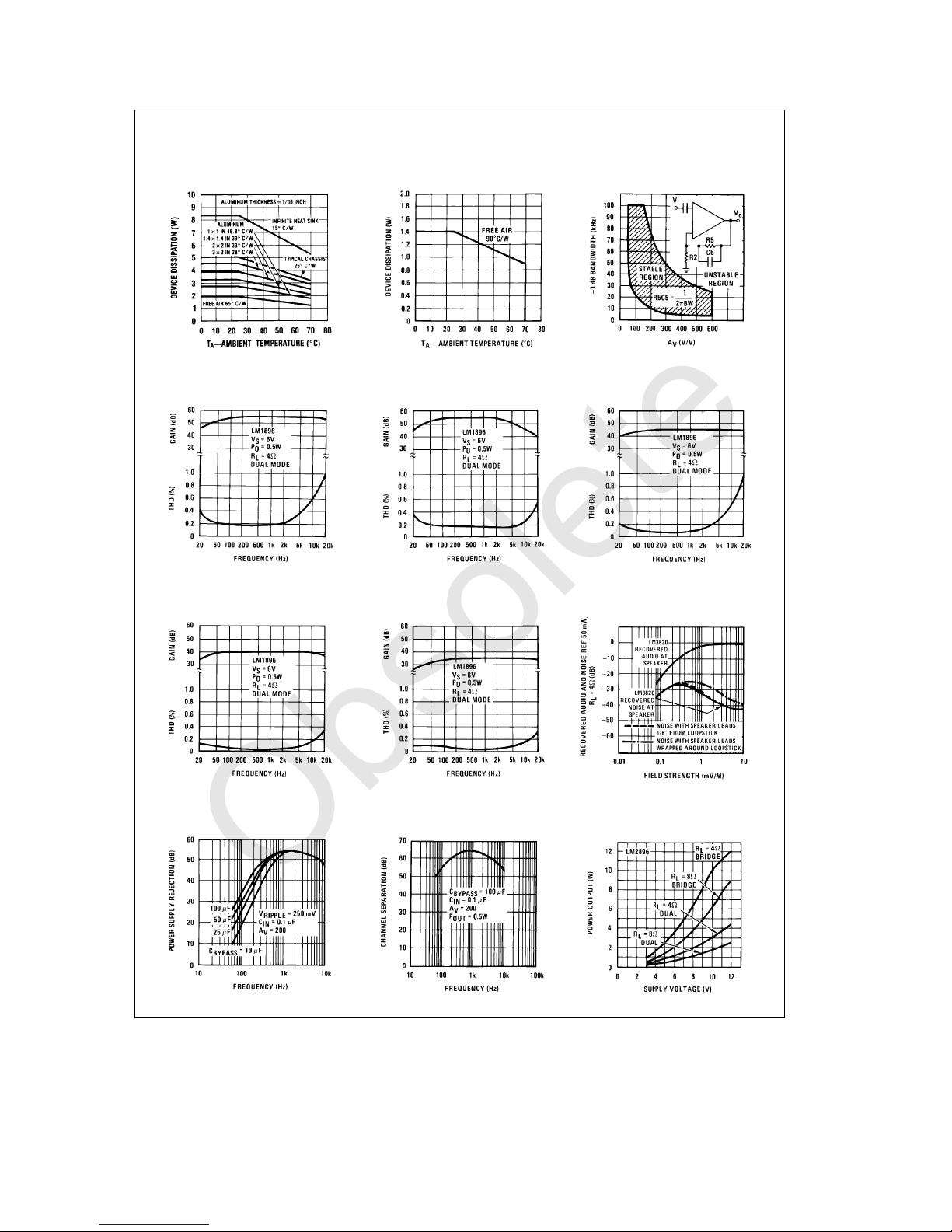
Typical Performance Curves
Obsolete
LM2896 Device Dissipation
vs Ambient Temperature
LM1896 Maximum Device
Dissipation vs Ambient
Temperature
b
3 dB Bandwidth vs Voltage
Gain for Stable Operation
THD and Gain vs Frequency
e
A
54 dB, BWe30 kHz
V
THD and Gain vs Frequency
e
A
40 dB, BWe20 kHz
V
Power Supply Rejection Ratio
(Referred to the Output)
vs Frequency
THD and Gain vs Frequency
e
A
54 dB, BWe5 kHz
V
THD and Gain vs Frequency
e
A
34 dB, BWe50 kHz
V
Channel Separation (Referred
to the Output) vs Frequency
THD and Gain vs Frequency
e
A
46 dB, BWe50 kHz
V
AM Recovered Audio and Noise
vs Field Strength for Different
Speaker Lead Placement
Power Output vs
Supply Voltage
TL/H/7920– 2
3
Page 5

Typical Performance Curves (Continued)
Obsolete
Total Harmonic Distortion
vs Power Output
Power Dissipation vs
Power Output R
Equivalent Schematic
e
4X
L
Power Dissipation vs
Power Output R
e
L
TL/H/7920– 3
8X
6, 9 No connection on LM1896 TL/H/7920– 4
( ) indicates pin number for LM2896
Connection Diagrams
Single-In-Line Package
Dual-In-Line Package
Top View
TL/H/7920– 5
TL/H/7920– 6
Top View
4
Page 6

Typical Applications (Continued)
Obsolete
6, 9 No connection on LM1896
( ) Indicates pin number for LM2896
FIGURE 2. Stereo Amplifier with A
TL/H/7920– 7
e
200, BWe30 kHz
V
TL/H/7920– 8
External Components
Components Comments
1. R2, R5, R10, R13 Sets voltage gain, A
2. R3, R12 Bootstrap resistor sets drive current for output stage and allows pins 3 and 12 to
3. R
o
4. C1, C14 Input coupling capacitor. Pins 1 and 14 are at a DC potential of V
5. C2, C13 Feedback capacitors. Ensure unity gain at DC. Also a low frequency pole at:
6. C3, C12 Bootstrap capacitors, used to increase drive to output stage. A low frequency
7. C5, C10 Compensation capacitor. These stabilize the amplifiers and adjust their
8. C7 Improves power supply rejection (See Typical Performance Curves). Increasing
9. C
c
10. C
o
11. C
S
(Figure 2)
e1a
R5/R2 for one channel and A
for the other channel.
go above V
Works with Coto stabilize output stage.
frequency pole set by:
e
f
L
2q RINC1
e
f
L
2qR2C2
pole is set by:
e
f
L
2qR3C3
bandwidth. See curve of bandwidth vs allowable gain.
C7 increases turn-on delay.
Output coupling capacitor. Isolates pins 5 and 10 from the load. Low frequency
pole set by:
e
f
L
2q CcR
Works with Roto stabilize output stage.
Provides power supply filtering.
V
.
S
1
1
1
1
L
V
e1a
S
R10/R13
/2. Low
5
Page 7

Application Hints
Obsolete
AM Radios
The LM1896/LM2896 has been designed fo fill a wide
range of audio power applications. A common problem with
IC audio power amplifiers has been poor signal-to-noise performance when used in AM radio applications. In a typical
radio application, the loopstick antenna is in close proximity
to the audio amplifer. Current flowing in the speaker and
power supply leads can cause electromagnetic coupling to
the loopstick, resulting in system oscillation. In addition,
most audio power amplifiers are not optimized for lowest
noise because of compensation requirements. If noise from
the audio amplifier radiates into the AM section, the sensitivity and signal-to-noise ratio will be degraded.
The LM1896 exhibits extremely low wideband noise due in
part to an external capacitor C5 which is used to tailor the
bandwidth. The circuit shown in
signal-to-noise ratio in excess of 60 dB referred to 50 mW.
Capacitor C5 not only limits the closed loop bandwidth, it
also provides overall loop compensation. Neglecting C2 in
Figure 2
, the gain is:
(S)
A
V
R2aR5
where A
A curve of
Performance Curves.
Figure 3
field strength in mV/M. The receiver section in this example
is an LM3820. The power amplifier is located about two
inches from the loopstick antenna. Speaker leads run parallel to the loopstick and are 1/8 inch from it. Referenced to a
20 dB S/N ratio, the improvement in noise performance
over conventional designs is about 10 dB. This corresponds
to an increase in usable sensitivity of about 8.5 dB.
Bridge Amplifiers
The LM1896/LM2896 can be used in the bridge mode as a
monaural power amplifier. In addition to much higher power
output, the bridge configuration does not require output coupling capacitors. The load is connected directly between the
amplifier outputs as shown in
b
shows a plot of recovered audio as a function of
e
V
3dBBW(0o)vsAVis shown in the Typical
e
R2
SaA
a
S
Figure 4
Figure 2
V0o
0
o
,
0
o
.
is capable of a
1
e
R5C5
2#1
2q RBC
c
e
0.9 Watts
e
Figure 1
a
R5/R2. The output of
R5
a
R2
J
1
B
e
8X bridged, then the
L
2
6
e
2
20c4
0.707
2qRC
shows the complete
c
2
Amp 1 has a voltage gain set by 1
amp 1 drives amp 2 which is configured as an inverting
amplifier with unity gain. Because of this phase inversion in
amp 2, there isa6dBincrease in voltage gain referenced to
V
. The voltage gain in bridge is:
i
CBis used to prevent DC voltage on the output of amp 1
from causing offset in amp 2. Low frequency response is
influenced by:
Several precautions should be observed when using the
LM1896/LM2896 in bridge configuration. Because the amplifiers are driving the load out of phase, an 8X speaker will
appear as a 4X load, and a 4X speaker will appear as a 2X
load. Power dissipation is twice as severe in this situation.
For example, if V
maximum dissipation is:
This amount of dissipation is equivalent to driving two 4X
loads in the stereo configuration.
When adjusting the frequency response in the bridge configuration, R5C5 and R10C10 form a 2 pole cascade and the
b
3 dB bandwidth is actually shifted to a lower frequency:
where Refeedback resistor
Cefeedback capacitor
To measure the output voltage, a floating or differential meter should be used because a prolonged output short will
over dissipate the package.
bridge amplifier.
V
o
e
V
i
e
f
L
e
6V and R
S
2
V
S
e
P
D
20 R
L
P
D
BW
FIGURE 3. Improved AM Sensitivity over Conventional Design
TL/H/7920– 9
6
Page 8

Application Hints (Continued)
Obsolete
Figure 4. Bridge Amplifier Connection
Printed Circuit Layout
Printed Circuit Board Layout
Figure 5
and
Figure 6
the LM1896 and LM2896. The circuits are wired as stereo
amplifiers. The signal source ground should return to the
input ground shown on the boards. Returning the loads to
power supply ground through a separate wire will keep the
THD at its lowest value. The inputs should be terminated in
show printed circuit board layouts for
TL/H/7920– 10
less than 50 kX to prevent an input-output oscillation. This
oscillation is dependent on the gain and the proximity of the
bridge elements R
mode is not used, do not insert R
To wire the amplifer into the bridge configuration, short the
capacitor on pin 7 (pin 1 of the LM1896) to ground. Connect
together the nodes labeled BRIDGE and drive the capacitor
connected to pin 5 (pin 14 of the LM1896).
and CBto the (a) input. If the bridge
B
B,CB
into the PCB.
FIGURE 5. Printed Circuit Board Layout for the LM1896
TL/H/7920– 11
7
Page 9

Printed Circuit Layout (Continued)
Obsolete
FIGURE 6. Printed Circuit Board Layout for the LM2896
8
TL/H/7920– 12
Page 10

Physical Dimensions inches (millimeters)
Obsolete
Molded Dual-In-Line Package (N)
Order Number LM1896N
See NS Package Number N14A
9
Page 11

Physical Dimensions inches (millimeters) (Continued)
Obsolete
LM1896/LM2896 Dual Audio Power Amplifier
Single-In-Line Package (P)
Order Number LM2896P
NS Package Number P11A
LIFE SUPPORT POLICY
NATIONAL’S PRODUCTS ARE NOT AUTHORIZED FOR USE AS CRITICAL COMPONENTS IN LIFE SUPPORT
DEVICES OR SYSTEMS WITHOUT THE EXPRESS WRITTEN APPROVAL OF THE PRESIDENT OF NATIONAL
SEMICONDUCTOR CORPORATION. As used herein:
1. Life support devices or systems are devices or 2. A critical component is any component of a life
systems which, (a) are intended for surgical implant support device or system whose failure to perform can
into the body, or (b) support or sustain life, and whose be reasonably expected to cause the failure of the life
failure to perform, when properly used in accordance support device or system, or to affect its safety or
with instructions for use provided in the labeling, can effectiveness.
be reasonably expected to result in a significant injury
to the user.
National Semiconductor National Semiconductor National Semiconductor National Semiconductor
Corporation Europe Hong Kong Ltd. Japan Ltd.
1111 West Bardin Road Fax: (
Arlington, TX 76017 Email: cnjwge@tevm2.nsc.com Ocean Centre, 5 Canton Rd. Fax: 81-043-299-2408
Tel: 1(800) 272-9959 Deutsch Tel: (
Fax: 1(800) 737-7018 English Tel: (
National does not assume any responsibility for use of any circuitry described, no circuit patent licenses are implied and National reserves the right at any time without notice to change said circuitry and specifications.
Fran3ais Tel: (
Italiano Tel: (
a
49) 0-180-530 85 86 13th Floor, Straight Block, Tel: 81-043-299-2309
a
49) 0-180-530 85 85 Tsimshatsui, Kowloon
a
49) 0-180-532 78 32 Hong Kong
a
49) 0-180-532 93 58 Tel: (852) 2737-1600
a
49) 0-180-534 16 80 Fax: (852) 2736-9960
Page 12

IMPORTANT NOTICE
Texas Instruments Incorporated and its subsidiaries (TI) reserve the right to make corrections, modifications, enhancements, improvements,
and other changes to its products and services at any time and to discontinue any product or service without notice. Customers should
obtain the latest relevant information before placing orders and should verify that such information is current and complete. All products are
sold subject to TI’s terms and conditions of sale supplied at the time of order acknowledgment.
TI warrants performance of its hardware products to the specifications applicable at the time of sale in accordance with TI’s standard
warranty. Testing and other quality control techniques are used to the extent TI deems necessary to support this warranty. Except where
mandated by government requirements, testing of all parameters of each product is not necessarily performed.
TI assumes no liability for applications assistance or customer product design. Customers are responsible for their products and
applications using TI components. To minimize the risks associated with customer products and applications, customers should provide
adequate design and operating safeguards.
TI does not warrant or represent that any license, either express or implied, is granted under any TI patent right, copyright, mask work right,
or other TI intellectual property right relating to any combination, machine, or process in which TI products or services are used. Information
published by TI regarding third-party products or services does not constitute a license from TI to use such products or services or a
warranty or endorsement thereof. Use of such information may require a license from a third party under the patents or other intellectual
property of the third party, or a license from TI under the patents or other intellectual property of TI.
Reproduction of TI information in TI data books or data sheets is permissible only if reproduction is without alteration and is accompanied
by all associated warranties, conditions, limitations, and notices. Reproduction of this information with alteration is an unfair and deceptive
business practice. TI is not responsible or liable for such altered documentation. Information of third parties may be subject to additional
restrictions.
Resale of TI products or services with statements different from or beyond the parameters stated by TI for that product or service voids all
express and any implied warranties for the associated TI product or service and is an unfair and deceptive business practice. TI is not
responsible or liable for any such statements.
TI products are not authorized for use in safety-critical applications (such as life support) where a failure of the TI product would reasonably
be expected to cause severe personal injury or death, unless officers of the parties have executed an agreement specifically governing
such use. Buyers represent that they have all necessary expertise in the safety and regulatory ramifications of their applications, and
acknowledge and agree that they are solely responsible for all legal, regulatory and safety-related requirements concerning their products
and any use of TI products in such safety-critical applications, notwithstanding any applications-related information or support that may be
provided by TI. Further, Buyers must fully indemnify TI and its representatives against any damages arising out of the use of TI products in
such safety-critical applications.
TI products are neither designed nor intended for use in military/aerospace applications or environments unless the TI products are
specifically designated by TI as military-grade or "enhanced plastic." Only products designated by TI as military-grade meet military
specifications. Buyers acknowledge and agree that any such use of TI products which TI has not designated as military-grade is solely at
the Buyer's risk, and that they are solely responsible for compliance with all legal and regulatory requirements in connection with such use.
TI products are neither designed nor intended for use in automotive applications or environments unless the specific TI products are
designated by TI as compliant with ISO/TS 16949 requirements. Buyers acknowledge and agree that, if they use any non-designated
products in automotive applications, TI will not be responsible for any failure to meet such requirements.
Following are URLs where you can obtain information on other Texas Instruments products and application solutions:
Products Applications
Audio www.ti.com/audio Communications and Telecom www.ti.com/communications
Amplifiers amplifier.ti.com Computers and Peripherals www.ti.com/computers
Data Converters dataconverter.ti.com Consumer Electronics www.ti.com/consumer-apps
DLP® Products www.dlp.com Energy and Lighting www.ti.com/energy
DSP dsp.ti.com Industrial www.ti.com/industrial
Clocks and Timers www.ti.com/clocks Medical www.ti.com/medical
Interface interface.ti.com Security www.ti.com/security
Logic logic.ti.com Space, Avionics and Defense www.ti.com/space-avionics-defense
Power Mgmt power.ti.com Transportation and Automotive www.ti.com/automotive
Microcontrollers microcontroller.ti.com Video and Imaging www.ti.com/video
RFID www.ti-rfid.com
OMAP Mobile Processors www.ti.com/omap
Wireless Connectivity www.ti.com/wirelessconnectivity
TI E2E Community Home Page e2e.ti.com
Mailing Address: Texas Instruments, Post Office Box 655303, Dallas, Texas 75265
Copyright © 2011, Texas Instruments Incorporated
 Loading...