

Page 1

LDC2114 Evaluation Module for Inductive Touch Applications
User's Guide
Literature Number: SNOU144
December 2016
Page 2

Contents
1 Overview............................................................................................................................. 6
2 Compatible Sensor EVM ....................................................................................................... 7
3 Main EVM elements.............................................................................................................. 7
4 Sensing Solutions EVM GUI .................................................................................................. 8
4.1 System Requirements ................................................................................................... 8
4.2 Installation Instructions .................................................................................................. 9
4.3 Starting the GUI......................................................................................................... 16
4.4 Navigating the GUI ..................................................................................................... 17
4.5 Connecting the EVM ................................................................................................... 19
4.6 Configuring the EVM Using the Register Page..................................................................... 19
4.6.1 Automatically Update GUI Register Values Using Auto Read........................................ 19
4.6.2 Manually Update Device Register Values ............................................................... 20
4.6.3 Reading Register Values Without Auto Read........................................................... 22
4.6.4 Saving Device Configurations ............................................................................. 24
4.6.5 Loading Previously Saved Configurations............................................................... 24
4.7 Configuring the EVM Using the Configuration Page............................................................... 25
4.7.1 Changing registers through the Configuration Pane ................................................... 25
4.7.2 Selecting the Mode of Operation and Scan Rate....................................................... 26
4.7.3 Interrupt polarity............................................................................................. 26
4.7.4 Base-tracking Increment ................................................................................... 26
4.7.5 LC Resonant Frequency Divider (Pre-scaler)........................................................... 26
4.7.6 Channel Settings............................................................................................ 27
4.7.7 Algorithm Settings........................................................................................... 27
4.7.8 Calculator .................................................................................................... 27
4.7.9 Status......................................................................................................... 28
4.8 Streaming Measurement Data........................................................................................ 28
4.8.1 Choosing Visible Channels ................................................................................ 28
4.8.2 Logging Data to a File...................................................................................... 29
4.8.3 Starting and Stopping Data Streaming................................................................... 30
4.8.4 Data Statistics ............................................................................................... 31
4.8.5 Configuring the Graph...................................................................................... 32
4.8.6 Navigating the Data Streaming Buffer.................................................................... 34
4.9 Updating the EVM Firmware.......................................................................................... 36
5 LDC2114 EVM REV A Schematics and Layout........................................................................ 41
6 LDC2114EVM REV A Bill of Materials.................................................................................... 52
2
Table of Contents
Copyright © 2016, Texas Instruments Incorporated
SNOU144–December 2016
Submit Documentation Feedback
Page 3

www.ti.com
1 LDC2114 Evaluation Module............................................................................................... 6
2 Main EVM elements ......................................................................................................... 7
3 User Account Control Prompt.............................................................................................. 9
4 Software Installer Wizard.................................................................................................. 10
5 Software Installer License Agreement................................................................................... 10
6 Software Installation Directory............................................................................................ 11
7 Software Installer Ready .................................................................................................. 12
8 Software Installer in Progress ............................................................................................ 12
9 Device Driver Installer Wizard............................................................................................ 13
10 Device Driver Installer in Progress....................................................................................... 14
11 Device Driver Installer Completed ....................................................................................... 15
12 Software Installer Completed ............................................................................................. 15
13 Splash Screen .............................................................................................................. 16
14 Introduction Page........................................................................................................... 17
15 Mouse Hovered Over Menu Button...................................................................................... 18
16 Menu Display After Clicking Button...................................................................................... 18
17 EVM Connected to GUI ................................................................................................... 19
18 Selecting Auto Read Interval on Register Page ....................................................................... 20
19 Selecting a Register's Current Value for Editing on Register Page ................................................. 21
20 Hovering Mouse Over Register Bit Value on Register Page ........................................................ 22
21 Selecting a Register on Register Page.................................................................................. 23
22 Reading the Current Device Register Value on Register Page ..................................................... 23
23 Save Register Values to File on Register Page........................................................................ 24
24 Loading Previously Saved Register Values from File on Register Page ........................................... 25
25 Global Button Settings, Channel Settings on Configuration Page................................................... 26
26 Algorithm Settings and Calculator on Configuration Page............................................................ 27
27 Device Status ............................................................................................................... 28
28 Select the Data Graph on Data Streaming Page ...................................................................... 29
29 Select Log File Button on Data Streaming Page....................................................................... 30
30 Start Button on Data Streaming Page................................................................................... 31
31 Show Statistics Button on Data Streaming Page ...................................................................... 32
32 Hide Statistics Button on Data Streaming Page ....................................................................... 32
33 Show Graph Configuration Button on Data Streaming Page......................................................... 33
34 Graph Configuration Button on Data Streaming Page ................................................................ 34
35 Changing Number of Samples Displayed in Data Graph ............................................................ 35
36 Displaying Previous Data Samples on the Data Streaming Page ................................................... 36
37 Select TI-TXT File Button on Firmware Upload Page ................................................................ 37
38 Selecting TI-TXT Firmware File for Upload to EVM .................................................................. 38
39 Upload Firmware Button on Firmware Upload Page ................................................................. 39
40 Firmware Upload in Progress ............................................................................................ 39
41 Firmware Upload Success ............................................................................................... 40
42 Bridge between LDC and MSP430 ...................................................................................... 41
43 PU/PD for LDC inputs ..................................................................................................... 41
44 Power: 1.8V LDO for LDC211x........................................................................................... 42
45 Button press LEDs ......................................................................................................... 42
46 LDC2114 .................................................................................................................... 43
47 Level shift from 1.8V LDC211x to 3.3V MSP430 ...................................................................... 44
List of Figures
SNOU144–December 2016
Submit Documentation Feedback
Copyright © 2016, Texas Instruments Incorporated
List of Figures
3
Page 4

www.ti.com
48 Level shift for I2C........................................................................................................... 45
49 USB connector.............................................................................................................. 46
50 Power: 3.3V LDC for MSP430............................................................................................ 46
51 MSP430 ..................................................................................................................... 47
52 MSP430 GPIO Breakout connector and General purpose LEDs.................................................... 48
53 LDC2114 Layout Top Layer - Overview................................................................................. 49
54 LDC2114 Layout Top Layer – Signals and Components............................................................. 49
55 LDC2114 Layout MidLayer 1 – Ground Plane ......................................................................... 50
56 LDC2114 Layout MidLayer 2 – Signals and Power Plane............................................................ 50
57 LDC2114 Layout Bottom Layer – Signals Plane....................................................................... 51
58 LDC2114 Bottom Layer - Overview...................................................................................... 51
4
List of Figures
Copyright © 2016, Texas Instruments Incorporated
SNOU144–December 2016
Submit Documentation Feedback
Page 5

www.ti.com
1 List of Evaluation modules.................................................................................................. 6
2 Connection options ......................................................................................................... 7
3 BOM for LDC2114EVM rev A ............................................................................................ 52
List of Tables
SNOU144–December 2016
Submit Documentation Feedback
Copyright © 2016, Texas Instruments Incorporated
List of Tables
5
Page 6
1 Overview
The LDC2114 EVM demonstrates the use of inductive sensing technology to sense and measure the
presence or position of conductive target objects, and to detect the press of an inductive touch button. The
LDC is controlled by an MSP430, which interfaces to a host computer.
The LDC2112 is the two-channel version of the LDC2114. The LDC2112 does not have a dedicated EVM.
Instead, the four-channel LDC2114 EVM should be used to evaluate the technology and performance.
User's Guide
SNOU144–December 2016
LDC2114 Evaluation Module for Inductive Touch
Inductance to Digital Converter
Figure 1. LDC2114 Evaluation Module
PCB perforations allow removal of the microcontroller, so that a different microcontroller can be
connected.
This user guide covers the following EVMs:
Table 1. List of Evaluation modules
EVM name EVM revision Device under test
LDC2114EVM A LDC2114 WCSP
6
LDC2114 Evaluation Module for Inductive Touch Inductance to Digital Converter
Copyright © 2016, Texas Instruments Incorporated
SNOU144–December 2016
Submit Documentation Feedback
Page 7
www.ti.com
2 Compatible Sensor EVM
The EVM does not include any example sensors, but can easily be connected to sensors by using either
the ZIF connector or soldering wires to the header pins on the PCB. The LDC2114 EVM is compatible
with the LDCCOILEVM, which is available on the TI estore and contains 19 different sensor designs.
Connect sensors from the LDCCOILEVM with unshielded twisted pair wires to J6 of the LDC2114 EVM.
NOTE: Schematics, Layout, and Coil characteristics of the LDCCOILEVM are described in the
LDCCOILEVM user guide.
Table 2 shows the connection options for each coil type.
LDCTOUCHCOMCOILEVM coil type Connect to
A J3 ZIF connector using flat ribbon cable
B J3 ZIF connector using flat ribbon cable
C J3 ZIF connector using flat ribbon cable
D J3 ZIF connector using flat ribbon cable
E J6 2.54mm header using unshielded twisted pair wires
NOTE: When connecting the coil board to the EVM, it is recommended to attach the assembly to a
static object using tape or screws. This will prevent the cables from moving and potentially
changing the output code reading or reporting false triggers.
Compatible Sensor EVM
Table 2. Connection options
3 Main EVM elements
SNOU144–December 2016
Submit Documentation Feedback
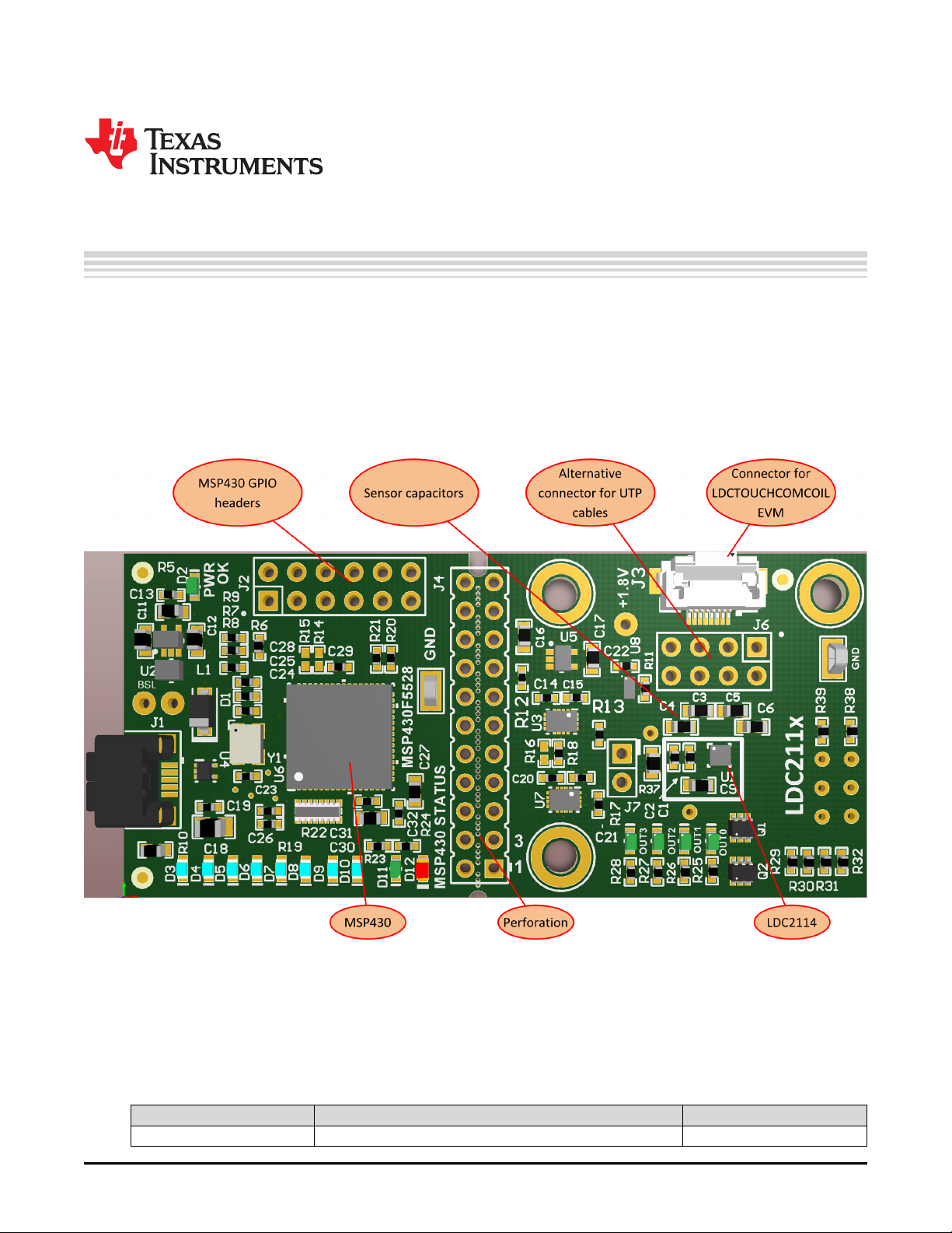
Figure 2. Main EVM elements
LDC2114 Evaluation Module for Inductive Touch Inductance to Digital
Copyright © 2016, Texas Instruments Incorporated
Converter
7
Page 8

Sensing Solutions EVM GUI
The EVM has the following features, as shown in Figure 2:
1. Power indication LED: this LED shows that the PCB is powered through the USB cable
2. MSP430 GPIO headers: This is a multi-purpose GPIO header which facilitates connection with a
second I2C interface, JTAG, UART, and three additional GPIOs. It also contains 5V, 3.3V, and GND
rails. These pins could be used for example to connect a haptics driver or an audio amplifier. Note that
functionality pof these pins is not implemented in the default EVM firmware.
3. Sensor capacitors: These are the sensor capacitors of the LDC2114. Replace them with suitable
values if appropriate.
4. Alternative connection for UTP cables: Custom sensors can be connected to these header
connections. Unshielded twisted pair (UTP) wires are the preferred wire choice for the sensor.
5. ZIF connector for LDCTOUCHCOMCOILEVM: Sensors of this PCB can be connected easily by
connecting the supplied flat ribbon cable.
6. BSL jumper connection: If firmware upgrade is unsuccessful, put the MSP430 into bootstrap loader
mode by shorting these two pins while powering up the EVM.
7. Micro-USB connector: connect to the PC using a micro-USB cable
8. Force touch LEDs: these eight LEDs show the intensity of the button press. They default firmware
chooses the channel with the strongest button push to indicate intensity.
9. MSP430 F5528: This microcontroller is used to configure the LDC2114, facilitate data streaming to the
GUI, and to show the intensity of the button press.
10. Perforation and probing header: These pads can be used for probing any signals between the
MSP430 and the LDC2114. It can be populated with a standard 2x11 pin 2.54mm header for ease of
access. It is also possible to break the LDC along the perforation and attach a different microcontroller
to these pins. The signals of the header are: [1-2]: OUT3, [3-4]: OUT2, [5-6]: OUT1, [7-8]: OUT0, [910]: INTB, [11-12]: LPWRB, [13-14]: SDA, [15-16]: SCL, [17-18]: GND, [19-20]: +3.3V, [21-22]: GND.
Note that the signals on this header are referenced to the Microcontroller VIO voltage (3.3V).
11. Button Press LEDs: These LEDs indicate which button has been pressed. Note that the MAXWIN
function is not enabled by default, so multiple buttons can be pressed simultaneously, and therefore
multiple LEDs may light up.
12. LDC2114: The LDC2114 Inductive Touch Inductance-to-Digital Converter for Consumer and LowPower Applications
13. LDC probing pads: These probing points use the level-shifted (1.8V referenced) signals of SDA, SCL,
OUT0, OUT1, OUT2, and OUT3
www.ti.com
4 Sensing Solutions EVM GUI
The Sensing Solutions EVM GUI provides direct device register access, user-friendly configuration, and
data streaming.
4.1 System Requirements
The host machine is required for device configuration and data streaming. The following steps are
necessary to prepare the EVM for the GUI:
• The GUI and EVM driver must be installed on a host computer.
• The EVM must be connected to a full speed USB port (USB 1.0 or above).
The Sensing Solutions EVM GUI supports the following operating systems (both 32-bit and 64-bit):
• Windows XP
• Windows 7
• Windows 8 and 8.1
• Windows 10
8
LDC2114 Evaluation Module for Inductive Touch Inductance to Digital
Converter
Copyright © 2016, Texas Instruments Incorporated
SNOU144–December 2016
Submit Documentation Feedback
Page 9
www.ti.com
4.2 Installation Instructions
The Sensing Solutions GUI and EVM driver installer is packaged in a zip file. Follow these steps to install
the software:
1. Download the latest version of the Sensing Solutions EVM GUI from EVM tool page.
NOTE: The minimum Sensing Solutions GUI revision for this EVM is 1.9.1. The latest GUI can be
downloaded here.
2. Extract the downloaded ZIP file.
3. Run the included executable.
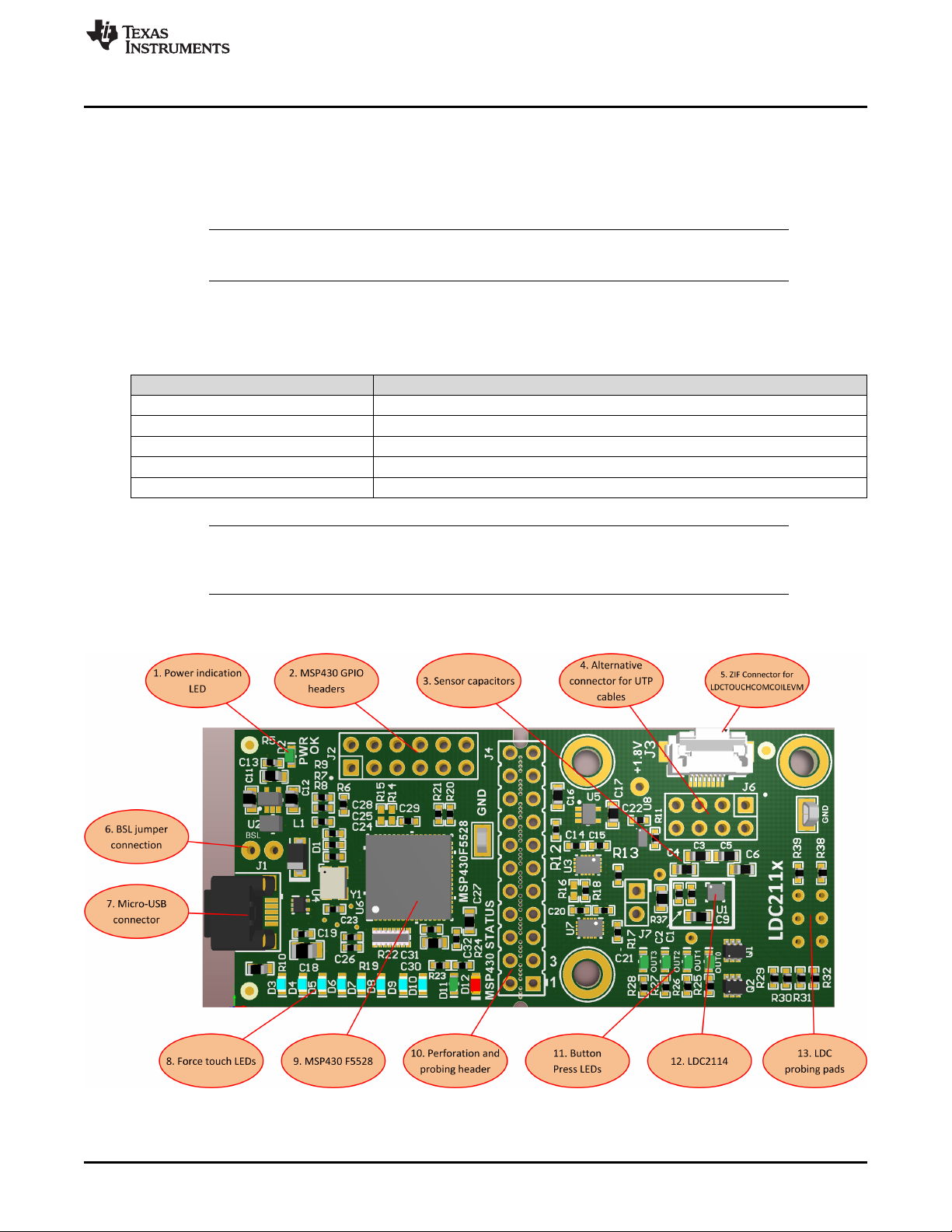
4. If prompted by the User Account Control about making changes to the computer, click Yes.
Sensing Solutions EVM GUI
Figure 3. User Account Control Prompt
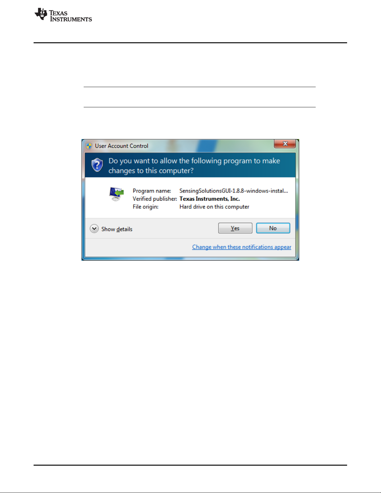
5. After the setup wizard starts, click Next.
SNOU144–December 2016
Submit Documentation Feedback
LDC2114 Evaluation Module for Inductive Touch Inductance to Digital
Copyright © 2016, Texas Instruments Incorporated
Converter
9
Page 10
Sensing Solutions EVM GUI
www.ti.com
Figure 4. Software Installer Wizard
6. Read the license agreement, select I accept the agreement, and click Next.
10
Figure 5. Software Installer License Agreement
LDC2114 Evaluation Module for Inductive Touch Inductance to Digital
Converter
Copyright © 2016, Texas Instruments Incorporated
SNOU144–December 2016
Submit Documentation Feedback
Page 11
www.ti.com
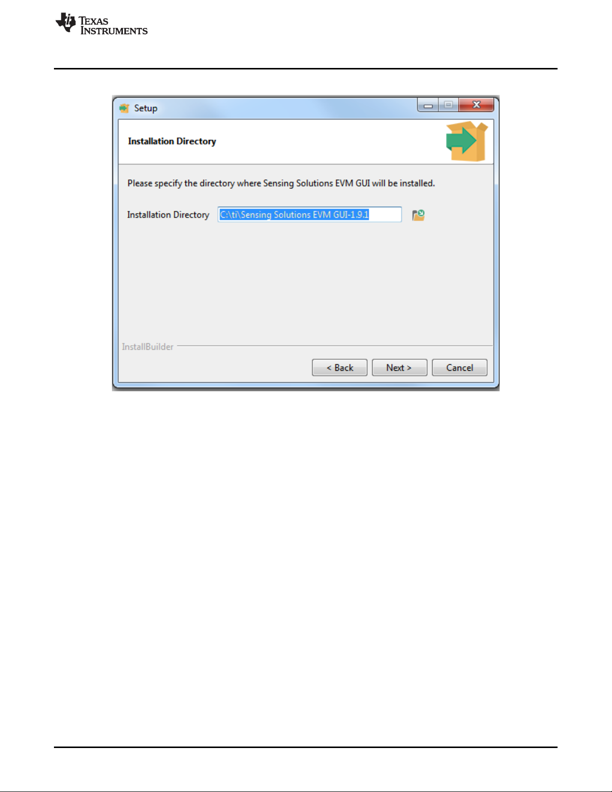
7. Use the preselected installation directory and click Next.
Sensing Solutions EVM GUI
Figure 6. Software Installation Directory
8. Start the installation by clicking Next.
SNOU144–December 2016
Submit Documentation Feedback
LDC2114 Evaluation Module for Inductive Touch Inductance to Digital
Copyright © 2016, Texas Instruments Incorporated
Converter
11
Page 12
Sensing Solutions EVM GUI
www.ti.com
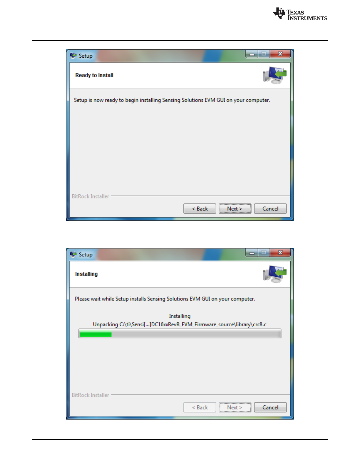
Figure 7. Software Installer Ready
9. Wait for the installation to complete.
12
Figure 8. Software Installer in Progress
LDC2114 Evaluation Module for Inductive Touch Inductance to Digital
Converter
Copyright © 2016, Texas Instruments Incorporated
SNOU144–December 2016
Submit Documentation Feedback
Page 13
www.ti.com
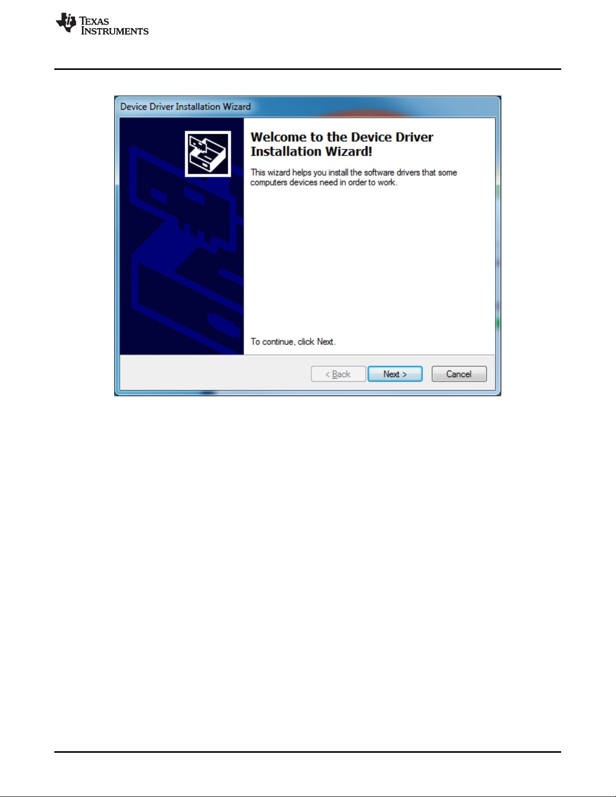
10. When the Device Driver Installation Wizard appears, click Next to install the EVM driver.
Sensing Solutions EVM GUI
Figure 9. Device Driver Installer Wizard
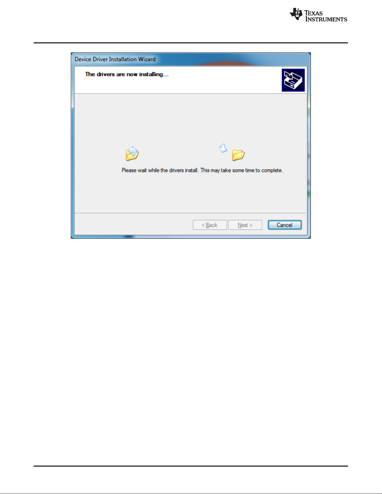
11. Wait for the driver installation to complete.
SNOU144–December 2016
Submit Documentation Feedback
LDC2114 Evaluation Module for Inductive Touch Inductance to Digital
Copyright © 2016, Texas Instruments Incorporated
Converter
13
Page 14
Sensing Solutions EVM GUI
www.ti.com
Figure 10. Device Driver Installer in Progress
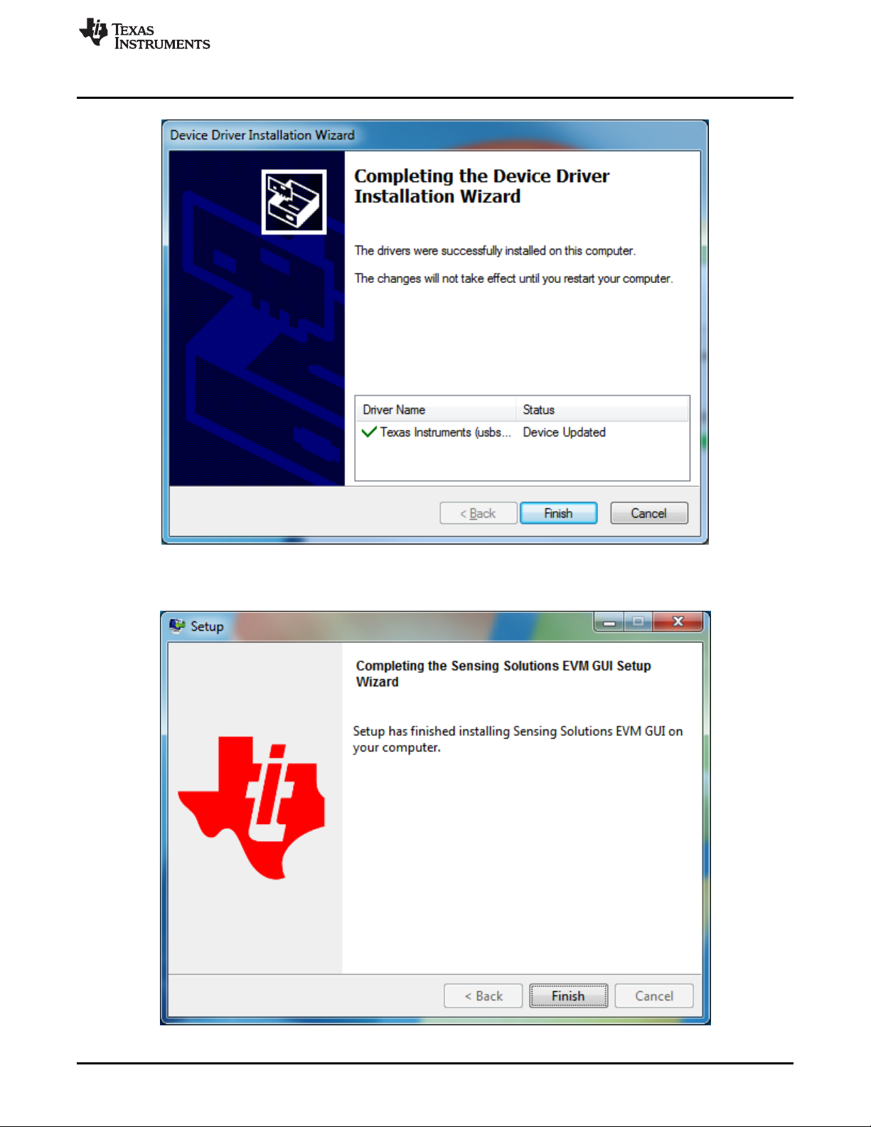
12. After the driver installation is completed, click Finish.
14
LDC2114 Evaluation Module for Inductive Touch Inductance to Digital
Converter
Copyright © 2016, Texas Instruments Incorporated
SNOU144–December 2016
Submit Documentation Feedback
Page 15
www.ti.com
Sensing Solutions EVM GUI
Figure 11. Device Driver Installer Completed
13. Click Finish to complete the installation.
SNOU144–December 2016
Submit Documentation Feedback
Figure 12. Software Installer Completed
LDC2114 Evaluation Module for Inductive Touch Inductance to Digital
Copyright © 2016, Texas Instruments Incorporated
Converter
15
Page 16
Sensing Solutions EVM GUI
4.3 Starting the GUI
Follow these steps to start the GUI:
1. Select the Windows start menu.
2. Select All programs.
3. Select Texas Instruments.
4. Select Sensing Solutions EVM GU.
5. Click Sensing Solutions EVM GU.
6. The splash screen will appear for at least two seconds.
www.ti.com
Figure 13. Splash Screen
7. After the splash screen is displayed the main window will open.
16
LDC2114 Evaluation Module for Inductive Touch Inductance to Digital
Converter
Copyright © 2016, Texas Instruments Incorporated
SNOU144–December 2016
Submit Documentation Feedback
Page 17
www.ti.com
Sensing Solutions EVM GUI
4.4 Navigating the GUI
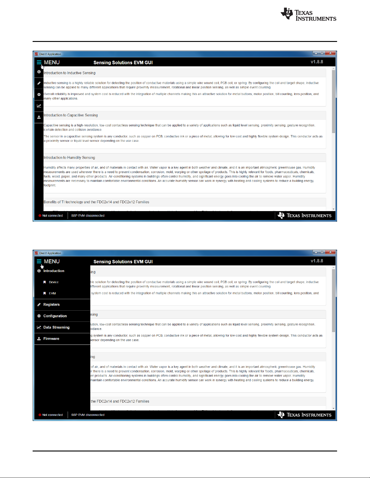
To navigate to different pages of the GUI follow these steps:
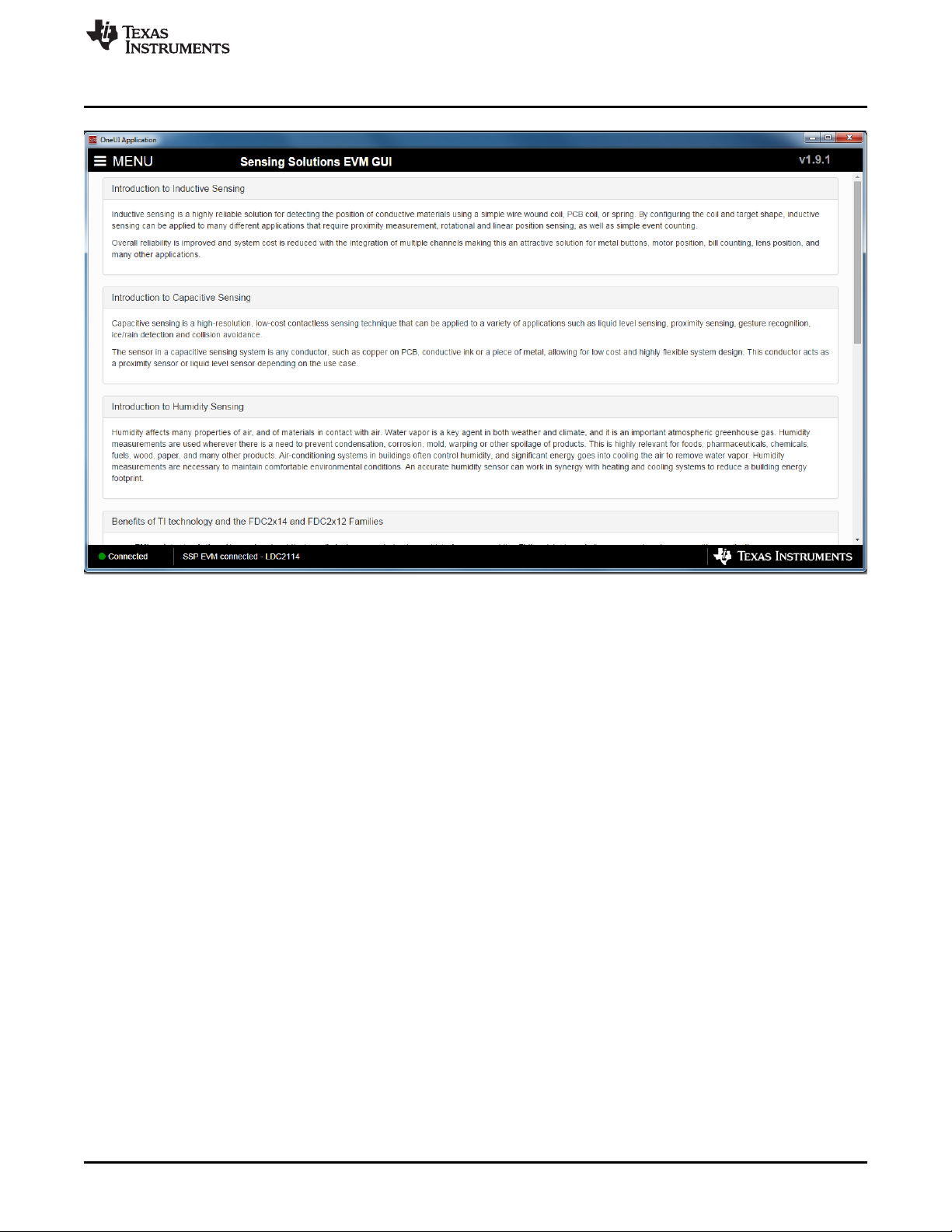
1. Click Menu in the upper left corner.
Figure 14. Introduction Page
SNOU144–December 2016
Submit Documentation Feedback
LDC2114 Evaluation Module for Inductive Touch Inductance to Digital
Copyright © 2016, Texas Instruments Incorporated
Converter
17
Page 18
Sensing Solutions EVM GUI
www.ti.com
Figure 15. Mouse Hovered Over Menu Button
2. Select the desired page from the menu shown on the left.
18
Figure 16. Menu Display After Clicking Button
LDC2114 Evaluation Module for Inductive Touch Inductance to Digital
Converter
Copyright © 2016, Texas Instruments Incorporated
SNOU144–December 2016
Submit Documentation Feedback
Page 19

www.ti.com
4.5 Connecting the EVM
Follow these steps to connect the EVM to the GUI:
1. Attach the EVM to the computer through USB.
2. The GUI always shows the connection status on the bottom left corner of the GUI.
Sensing Solutions EVM GUI
Figure 17. EVM Connected to GUI
4.6 Configuring the EVM Using the Register Page
The register page allows users to control the device directly with the register values. The user may also
use this page to read the current register values on the device.
4.6.1 Automatically Update GUI Register Values Using Auto Read
Auto read will periodically request the register values on the device. Click the drop down box next to Auto
Read to select the update interval.
SNOU144–December 2016
Submit Documentation Feedback
LDC2114 Evaluation Module for Inductive Touch Inductance to Digital
Copyright © 2016, Texas Instruments Incorporated
Converter
19
Page 20

Sensing Solutions EVM GUI
www.ti.com
Figure 18. Selecting Auto Read Interval on Register Page
4.6.2 Manually Update Device Register Values
There are two methods to change register values: update the entire register value or change a single bit
within the register. The recommended update mode is always Immediate and not Deferred. To update
register values, follow these steps.
1. Double-click the current value of the register that needs to be changed. The text will turn into an
editable text box.
20
LDC2114 Evaluation Module for Inductive Touch Inductance to Digital
Converter
Copyright © 2016, Texas Instruments Incorporated
SNOU144–December 2016
Submit Documentation Feedback
Page 21

www.ti.com
Sensing Solutions EVM GUI
Figure 19. Selecting a Register's Current Value for Editing on Register Page
2. Type the new hexadecimal value into the box and click enter. The text box changes to normal text and
the GUI will send a command to the EVM to update the device register.
To change individual bit values rather that entire register values follow these steps.
1. Hover the mouse over the desired bit to change.
SNOU144–December 2016
Submit Documentation Feedback
LDC2114 Evaluation Module for Inductive Touch Inductance to Digital
Copyright © 2016, Texas Instruments Incorporated
Converter
21
Page 22

Sensing Solutions EVM GUI
www.ti.com
Figure 20. Hovering Mouse Over Register Bit Value on Register Page
2. Double-click the bit to toggle its value and the register’s current value will update automatically.
4.6.3 Reading Register Values Without Auto Read
To read register values follow these steps.
1. Select the register to update by clicking any column of the register row in the table.
22
LDC2114 Evaluation Module for Inductive Touch Inductance to Digital
Converter
Copyright © 2016, Texas Instruments Incorporated
SNOU144–December 2016
Submit Documentation Feedback
Page 23

www.ti.com
Sensing Solutions EVM GUI
Figure 21. Selecting a Register on Register Page
2. Click the Read Register button to update the selected register’s current value and bit values in the
table.
Figure 22. Reading the Current Device Register Value on Register Page
SNOU144–December 2016
Submit Documentation Feedback
LDC2114 Evaluation Module for Inductive Touch Inductance to Digital
Copyright © 2016, Texas Instruments Incorporated
Converter
23
Page 24

Sensing Solutions EVM GUI
4.6.4 Saving Device Configurations
To save the current register settings of the device follow these steps.
1. Click the button immediately right to the Auto Read selection drop down.
www.ti.com
Figure 23. Save Register Values to File on Register Page
2. Choose a name for the JSON file and the directory to save it within. Then click Save.
4.6.5 Loading Previously Saved Configurations
To load previously saved register settings from a JSON file follow these steps.
1. Click the button furthest right from the Auto Read selection drop down.
24
LDC2114 Evaluation Module for Inductive Touch Inductance to Digital
Converter
Copyright © 2016, Texas Instruments Incorporated
SNOU144–December 2016
Submit Documentation Feedback
Page 25

www.ti.com
Sensing Solutions EVM GUI
Figure 24. Loading Previously Saved Register Values from File on Register Page
2. Select the JSON file with the desired settings and click Open.
4.7 Configuring the EVM Using the Configuration Page
The Sensing Solutions GUI is capable to configure the device in a more intuitive way than through the
direct register values. The Configuration page provides an easy-to-use tool for updating the device
configuration and provides additional information about how the device will perform.
4.7.1 Changing registers through the Configuration Pane
The device configuration must only be changed while STATE_RESET=b1. This mode can be entered
while selecting the appropriate option in the Reset Mode section of the Global Buttons Settings. After
changing the configuration, the Reset Mode must be changed back to Active processing, as shown in
Figure 25.
SNOU144–December 2016
Submit Documentation Feedback
LDC2114 Evaluation Module for Inductive Touch Inductance to Digital
Copyright © 2016, Texas Instruments Incorporated
Converter
25
Page 26

Sensing Solutions EVM GUI
www.ti.com
Figure 25. Global Button Settings, Channel Settings on Configuration Page
4.7.2 Selecting the Mode of Operation and Scan Rate
Each channel on the LDC2114 can be configured to operate either in Normal power mode or in Low
power mode. The Global Button Settings menu contains Normal Power Mode Scan Rate and Low Power
Mode Scan Rate selections, in which the desired scan rate chan be chosen for each mode of operation.
Channels can be assigned to either the Normal Power Mode or the Low Power Mode by toggling the Low
Power button in the Channel Settings table for each channel individually.
4.7.3 Interrupt polarity
The LDC interrupt pin polarity can be chosen in the 'Interrupt Polarity' option of the 'Global Buttons
Settings' section.
4.7.4 Base-tracking Increment
The LDC incorporates a baseline tracking algorithm to automatically compensate for any slow change in
the sensor output caused by environmental variations, such as temperature drift. The baseline tracking is
configured independently for Normal Power Mode and Low Power Mode. The increment for this feature is
configured in the Base-tracking Increment option.
4.7.5 LC Resonant Frequency Divider (Pre-scaler)
The LCDIV field sets the oscillation frequency divider. This field should be set as described in section
Programmable button sampling window of the LDC2114 datasheet.
26
LDC2114 Evaluation Module for Inductive Touch Inductance to Digital
Converter
Copyright © 2016, Texas Instruments Incorporated
SNOU144–December 2016
Submit Documentation Feedback
Page 27

www.ti.com
4.7.6 Channel Settings
In the Channel Settings section, each channel can be configured independently. Each channel has its own
enable bit and its own output pin with configurable polarity. The remaining parameters (Frequency, RP,
Gain, Counter Scale, Sensor Cycle Count, and Fast Tracking Factor) should be configured according to
the characteristics of the attached sensor.
4.7.7 Algorithm Settings
The LDC has four additional algorithms, which can be enabled in the Algorithms Settings section, as
shown in Figure 26.
1. The Max-Win algorithm enables the system to select the button pressed with maximum force when
multiple buttons are pressed at the same time. This feature must be enabled for each applicable
channel individually.
2. The Anti-Common Mode algorithm eliminates false detection when a user presses the panel in certain
positions, which could cause a common-mode change to two or more buttons. This feature must be
enabled for each applicable channel individually.
3. The Anti-Deform algorithm filters changes due to metal deformation in the vicinity of one or more
buttons. Such metal deformation can be accidentally caused by pressing a neighboring button that
does not have sufficient mechanical isolation. This feature must be enabled for each applicable
channel individually.
4. The Anti-twist algorithm reduces the likelihood of false detection when the case is twisted, which could
cause unintended mechanical activation of the buttons, or an opposite reaction in two adjacent buttons.
The anti-twist function can be enabled by configuring the ANTITWST setting to a value larger than 0.
Sensing Solutions EVM GUI
4.7.8 Calculator
The Calculator does not write any registers and is used for information purposes only. It calculates the
time of the sampling window for each channel based on its configured register settings.
Figure 26. Algorithm Settings and Calculator on Configuration Page
SNOU144–December 2016
Submit Documentation Feedback
LDC2114 Evaluation Module for Inductive Touch Inductance to Digital
Copyright © 2016, Texas Instruments Incorporated
Converter
27
Page 28

Sensing Solutions EVM GUI
4.7.9 Status
The Status section, as shown in Figure 27, reports the flags in the STATUS register of the LDC2114.
www.ti.com
4.8 Streaming Measurement Data
The Sensing Solutions GUI and EVM provide a tool to capture, display, and log measurement data. The
section describes how to use the data measurement tools from the Data Streaming page accessible from
the GUI menu.
4.8.1 Choosing Visible Channels
To select which channel measurements are displayed in the graph, check or uncheck the available
channels shown next to the graph units. Selecting or not selecting the channels only affects the graph and
not the data logged to a file. If a channel is not enabled in the Configuration page it will not appear on the
Data Streaming page. Figure 28 shows a streaming window in which channel 0 and channel 1 are
enabled, and channel 1 shows a button press.
Figure 27. Device Status
28
LDC2114 Evaluation Module for Inductive Touch Inductance to Digital
Converter
Copyright © 2016, Texas Instruments Incorporated
SNOU144–December 2016
Submit Documentation Feedback
Page 29

www.ti.com
Sensing Solutions EVM GUI
Figure 28. Select the Data Graph on Data Streaming Page
4.8.2 Logging Data to a File
Follow these steps to log measurement data to a file.
1. Click the button in the upper right under next to Click to Select Log File.
SNOU144–December 2016
Submit Documentation Feedback
LDC2114 Evaluation Module for Inductive Touch Inductance to Digital
Copyright © 2016, Texas Instruments Incorporated
Converter
29
Page 30

Sensing Solutions EVM GUI
www.ti.com
Figure 29. Select Log File Button on Data Streaming Page
2. Select a file name and directory to save the data to and then click the Save button.
3. Whenever data streaming is running the data for all channels will be logged to this file. The selected
file is shown next to the button.
4.8.3 Starting and Stopping Data Streaming
To start data streaming click the Start button.
30
LDC2114 Evaluation Module for Inductive Touch Inductance to Digital
Converter
Copyright © 2016, Texas Instruments Incorporated
SNOU144–December 2016
Submit Documentation Feedback
Page 31

www.ti.com
Sensing Solutions EVM GUI
To stop data streaming click the Stop button.
4.8.4 Data Statistics
Click the Show Statistics button to view the measurement statistics. Click the Hide Statistics button to hide
the measurement statistics.
Figure 30. Start Button on Data Streaming Page
SNOU144–December 2016
Submit Documentation Feedback
LDC2114 Evaluation Module for Inductive Touch Inductance to Digital
Copyright © 2016, Texas Instruments Incorporated
Converter
31
Page 32

Sensing Solutions EVM GUI
www.ti.com
Figure 31. Show Statistics Button on Data Streaming Page
Figure 32. Hide Statistics Button on Data Streaming Page
4.8.5 Configuring the Graph
To configure the graph, click the Show Graph Configuration button.
32
LDC2114 Evaluation Module for Inductive Touch Inductance to Digital
Converter
Copyright © 2016, Texas Instruments Incorporated
SNOU144–December 2016
Submit Documentation Feedback
Page 33

www.ti.com
Sensing Solutions EVM GUI
Figure 33. Show Graph Configuration Button on Data Streaming Page
SNOU144–December 2016
Submit Documentation Feedback
LDC2114 Evaluation Module for Inductive Touch Inductance to Digital
Copyright © 2016, Texas Instruments Incorporated
Converter
33
Page 34

Sensing Solutions EVM GUI
www.ti.com
Figure 34. Graph Configuration Button on Data Streaming Page
The configuration window displays the actual frame rate of the graph, the rate at which data is added to
the graph, the vertical scaling, and the sample buffer size. The display rate is the rate at which the graph
updates on the computer display and is not configurable. It is automatically optimized by the GUI.
The New Data Sample Rate allows the user to choose when new data is added to the graph. Selecting
EVM Output Rate will display data on the graph as fast as is available from the EVM. This should not be
confused with the actual sampling rate of the device on the EVM which could be different. The Add
sample to graph every ... ms will add a new sample to the graph at the specified rate.
The Vertical Scaling allows the user to either manually set the minimum and maximum values of the y-axis
on the graph or use auto-scaling. The Autoscale & Lock button scales the graph based on the data of the
current display and then locks those vertical scaling settings.
The Sample Counts allows the user to specify the number of samples displayed on the graph and the total
number of samples stored in the buffer. Please note the buffer size does not affect data logging to a file.
To hide the configuration window, click the Hide Graph Configuration button.
4.8.6 Navigating the Data Streaming Buffer
The Sensing Solutions EVM GUI stores a buffer of data samples and then displays a subset of those
samples. The data buffer can be navigated using the horizontal slider below the graph. To show more
samples on the graph, click either the slider on the left or right side of the green bar and drag it closer or
further from the other slider. The number of samples displayed is shown between the left and right sliders
in the green bar.
34
LDC2114 Evaluation Module for Inductive Touch Inductance to Digital
Converter
Copyright © 2016, Texas Instruments Incorporated
SNOU144–December 2016
Submit Documentation Feedback
Page 35

www.ti.com
Sensing Solutions EVM GUI
Figure 35. Changing Number of Samples Displayed in Data Graph
By clicking on the green bar and dragging the mouse left or right, previous samples in the buffer can be
displayed.
SNOU144–December 2016
Submit Documentation Feedback
LDC2114 Evaluation Module for Inductive Touch Inductance to Digital
Copyright © 2016, Texas Instruments Incorporated
Converter
35
Page 36

Sensing Solutions EVM GUI
www.ti.com
Figure 36. Displaying Previous Data Samples on the Data Streaming Page
4.9 Updating the EVM Firmware
To upload new firmware to the EVM, navigate to the Firmware page from the GUI menu and follow these
steps. The images below show uploading the FDC2214 EVM firmware, but the steps are identical for any
LDC, FDC, or HDC EVM when using their respective firmware files.
1. Click the button to select a TI-TXT firmware file.
36
LDC2114 Evaluation Module for Inductive Touch Inductance to Digital
Converter
Copyright © 2016, Texas Instruments Incorporated
SNOU144–December 2016
Submit Documentation Feedback
Page 37

www.ti.com
Sensing Solutions EVM GUI
Figure 37. Select TI-TXT File Button on Firmware Upload Page
2. Select the firmware file and click Open.
SNOU144–December 2016
Submit Documentation Feedback
LDC2114 Evaluation Module for Inductive Touch Inductance to Digital
Copyright © 2016, Texas Instruments Incorporated
Converter
37
Page 38

Sensing Solutions EVM GUI
www.ti.com
Figure 38. Selecting TI-TXT Firmware File for Upload to EVM
3. Click the Upload Firmware button.
38
LDC2114 Evaluation Module for Inductive Touch Inductance to Digital
Converter
Copyright © 2016, Texas Instruments Incorporated
SNOU144–December 2016
Submit Documentation Feedback
Page 39

www.ti.com
Sensing Solutions EVM GUI
Figure 39. Upload Firmware Button on Firmware Upload Page
4. Wait for the firmware to upload. Do NOT disconnect the EVM from the PC at this time! Also note that
the GUI will disconnect from the EVM. The upload process should not take more than one minute. If
the upload fails or lasts longer than one minute, unplug the EVM and restart the GUI.
SNOU144–December 2016
Submit Documentation Feedback
Figure 40. Firmware Upload in Progress
LDC2114 Evaluation Module for Inductive Touch Inductance to Digital
Copyright © 2016, Texas Instruments Incorporated
Converter
39
Page 40

Sensing Solutions EVM GUI
www.ti.com
Figure 41. Firmware Upload Success
40
LDC2114 Evaluation Module for Inductive Touch Inductance to Digital
Converter
Copyright © 2016, Texas Instruments Incorporated
SNOU144–December 2016
Submit Documentation Feedback
Page 41

PU/PD for LDC inputs
Layout note: move to bottom side
0
R33
0
R35
+1.8V
GND
LPWRB
0
R34
0
R36
+1.8V
GND
OUT3/ADDR
Design note: Do not populate R34 or R36 for LDC2114
Copyright © 2016, Texas Instruments Incorporated
OUT0_3.3
OUT1_3.3
OUT2_3.3
OUT3/ADDR_3.3
INTB_3.3
LPWRB_3.3
GND
GND
+3.3V+3.3V
GND
GND
Layout note: Perforate PCB along this header
Bridge between LDC and MSP430
INTB_3.3
LPWRB_3.3
SDA_3.3
SCL_3.3
OUT0_3.3
OUT1_3.3
OUT2_3.3
OUT3/ADDR_3.3
Layout note: Route traces between L & R header columns on inner layers
GND2
SDA_3.3
SCL_3.3
1 2
3 4
5 6
7 8
9 10
11 12
13 14
15
17
19
21
16
18
20
22
J4
TSW-111-07-G-D
Copyright © 2016, Texas Instruments Incorporated
www.ti.com
5 LDC2114 EVM REV A Schematics and Layout
Figure 42. Bridge between LDC and MSP430
LDC2114 EVM REV A Schematics and Layout
SNOU144–December 2016
Submit Documentation Feedback
Figure 43. PU/PD for LDC inputs
LDC2114 Evaluation Module for Inductive Touch Inductance to Digital Converter
Copyright © 2016, Texas Instruments Incorporated
41
Page 42

GND
OUT0
GND GND GND
OUT3/ADDR
Green
1
2
D13
Green
1
2
D14
Green
1
2
D15
Green
1
2
D16
OUT1 OUT2
3
5
4
Q1A
MMDT3904-7-F
6
2
1
Q1B
MMDT3904-7-F
3
5
4
Q2A
MMDT3904-7-F
6
2
1
Q2B
MMDT3904-7-F
+3.3V +3.3V +3.3V +3.3V
402
R25
402
R26
402
R27
402
R28
4.70k
R29
4.70k
R30
4.70k
R31
4.70k
R32
Design note: 4mA
Button press LEDs
Design note: OUTPUTS must be configured as active high in device register settings
Copyright © 2016, Texas Instruments Incorporated
IN1OUT
5
2
EN
3
NC
4
GND
U5
LP5951MG-1.8/NOPB
+3.3V
2.2µF
C17
+1.8V
GND
GND
2.2µF
C16
GND
Power: 1.8V LDO for LDC211x
TP2
Copyright © 2016, Texas Instruments Incorporated
LDC2114 EVM REV A Schematics and Layout
www.ti.com
Figure 44. Power: 1.8V LDO for LDC211x
42
LDC2114 Evaluation Module for Inductive Touch Inductance to Digital Converter
Figure 45. Button press LEDs
Copyright © 2016, Texas Instruments Incorporated
SNOU144–December 2016
Submit Documentation Feedback
Page 43

IN0
IN0
IN1
IN2
IN3
Sensor connectors
LPWRB
INTB
SCL
OUT0
SDA
OUT1
OUT2
OUT3/ADDR
IN2
IN1
IN0
GND
+1.8V
COM
GND GND
LDC211x
+1.8V
4.7k
R38
4.7k
R39
+1.8V
SCL
D3
SDA
C3
INT
B2
LPWR
C2
VDD
C1
GND
D1
GND
A4
COM
D2
IN0
A3
IN1
A2
IN2
A1
IN3
B1
OUT0
D4
OUT1
C4
OUT2
B4
OUT3
B3
U1
LDC2114YFDR
IN3
IN2
IN1
1 2
3 4
5 6
7 8
J6
0
R37
1
2
J7
TSW-102-07-G-S
Layout note: move C1,C2,C3,C4 close to DUT
1µF
C2
0.1µF
C1
47pF
C6
47pFC547pFC347pF
C4
GND
IN3
COM
TP9 TP10 TP11TP1
TP12 TP13
COM
1000pF
C9
TP14 TP15
5
4
1
2
3
6
7
8
MP1
MP2
J3
Copyright © 2016, Texas Instruments Incorporated
www.ti.com
LDC2114 EVM REV A Schematics and Layout
Figure 46. LDC2114
SNOU144–December 2016
Submit Documentation Feedback
Copyright © 2016, Texas Instruments Incorporated
LDC2114 Evaluation Module for Inductive Touch Inductance to Digital Converter
43
Page 44

1A1
6
1OE
1
VCCB
2
1DIR
4
VCCA
3
2DIR
5
1A2
7
2A1
8
2A2
9
GND
10
GND
11
2B2
12
2B1
13
1B2
14
1B1
15
2OE
16
U3
SN74AVCH4T245RSVR
+1.8V+3.3V
0.1µF
C15
0.1µF
C14
LPWRB
+3.3V
INTB
GND
GND
GND
1A1
6
1OE
1
VCCB
2
1DIR
4
VCCA
3
2DIR
5
1A2
7
2A1
8
2A2
9
GND
10
GND
11
2B2
12
2B1
13
1B2
14
1B1
15
2OE
16
U7
SN74AVCH4T245RSVR
+1.8V+3.3V
0.1µF
C21
0.1µF
C20
OUT1
GND
GND
OUT1_3.3
OUT0_3.3 OUT0
GND
0
R18
+3.3V
GND
0
R17
OUT3/ADDR_3.3
OUT2_3.3
OUT2
INTB_3.3
LPWRB_3.3
Level shift from 1.8V LDC211x to 3.3V MSP430
Design note: DIR=Hi sends signals from Aports to B ports
Design note: PD for LDC2114, PU for LDC2112
Design note: UNPOP for LDC2112
Design note: Send INTB LDC2114->MSP430
Design note: Send LPWRB MSP430->LDC2114
GND
0
R16
Design note: DIR=Hi sends signals from Aports to B ports
OUT3/ADDR
Copyright © 2016, Texas Instruments Incorporated
LDC2114 EVM REV A Schematics and Layout
www.ti.com
44
LDC2114 Evaluation Module for Inductive Touch Inductance to Digital Converter
Figure 47. Level shift from 1.8V LDC211x to 3.3V MSP430
SNOU144–December 2016
Submit Documentation Feedback
Copyright © 2016, Texas Instruments Incorporated
Page 45

GND
A1
EN
A2
VREF1
B1
VREF2
B2
SCL1C1SCL2
C2
SDA1
D1
SDA2
D2
U8
PCA9306YZTR
GND
200k
R11
+3.3V
SCL
SDA
SCL_3.3
SDA_3.3
100pF
C22
+1.8V
GND
Level shift for I2C
Design note: MSP430: 3.3V, LDC211x: 1.8V
Design note: VREF2 must be 1.8V, 3.3V, or 5V if VREF1 = 1.8V
4.7k
R13
+3.3V +3.3V
4.7k
R12
Copyright © 2016, Texas Instruments Incorporated
www.ti.com
LDC2114 EVM REV A Schematics and Layout
Figure 48. Level shift for I2C
SNOU144–December 2016
Submit Documentation Feedback
Copyright © 2016, Texas Instruments Incorporated
LDC2114 Evaluation Module for Inductive Touch Inductance to Digital Converter
45
Page 46

GND
5.6V
D1
MMSZ5232B-7-F
GND
VBUS +5V
L1
VLS201610ET-100M
2.2µF
C13
+3.3V
GND
2.2µF
C12
GND
GND
IN1OUT
5
2
EN3NC
4
GND
U2
LP5951MG-3.3/NOPB
GND
Green
1
2
D2
402
R5
Power: 3.3V LDO for MSP430
GND
GND1
10µF
C11
Copyright © 2016, Texas Instruments Incorporated
USB connector
GND
0.1µF
C19
GND
1.5k
R6
1.00M
R9
GND
MSP_DM
33
R10
GND
22µF
C18
VCC
1
NC
2
IO1
3
GND
4
IO2
5
U4
TPD2E001DRLR
VBUS
GND
10.0
R7
10.0
R8
USB-D+
USB-D-
MSP_PUR
MSP_DP
Layout note: place U4, C18, C19, and D1 next to J1
VBUS
1
D-
2
D+
3
ID
4
GND
5
678
11109
J1
10118193-0001LF
Copyright © 2016, Texas Instruments Incorporated
LDC2114 EVM REV A Schematics and Layout
www.ti.com
Figure 49. USB connector
46
Figure 50. Power: 3.3V LDC for MSP430
LDC2114 Evaluation Module for Inductive Touch Inductance to Digital Converter
Copyright © 2016, Texas Instruments Incorporated
SNOU144–December 2016
Submit Documentation Feedback
Page 47

0.47µF
C27
GND
SDA_3.3
SCL_3.3
VUSB
GND
GND
MSP_DP
MSP_DM
MSP_PUR
JTAG_TDO
JTAG_TDI
JTAG_TMS
JTAG_TCK
JTAG_RST
JTAG_TEST
GND
+3.3V +3.3V +3.3V
0.1µF
C31
0.1µF
C32
0.1µF
C29
+5V
GNDGND
24MHz
1
34
2
G
G
Y1
ABM8-24.000MHZ-B2-T
GND
+3.3V +3.3V
33k
R19
+3.3V
0.22µF
C25
0.22µF
C28
Xtalin
Xtalout
18pF
C23
18pF
C24
P1.6
4.7k
R14
4.7k
R15
OUT3/ADDR_3.3
OUT2_3.3
OUT1_3.3
OUT0_3.3
VCORE
P2.0
P2.1
S1_LED
S2_LED
GND
SDA2
SCL2
Tx
Rx
TP4TP3
GND GND
1.0k
R24
Green
1
2
D11
Super Red
1
2
D12
S1_LEDS2_LED
402
R23
MSP430
INTB_3.3
LPWRB_3.3
VUSB
MSP_PUR
Silk: BSL
Layout note: place 100mil apart
P6.0/CB0/A0
1
P6.1/CB1/A1
2
P6.2/CB2/A2
3
P6.3/CB3/A3
4
P6.4/CB4/A4
5
P6.5/CB5/A5
6
P6.6/CB6/A6
7
P6.7/CB7/A7
8
P5.0/A8/VREF+/VEREF+
9
P5.1/A9/VREF-/VEREF-
10
AVCC1
11
P5.4/XIN
12
P5.5/XOUT
13
AVSS1
14
DVCC1
15
DVSS1
16
VCORE
17
P1.0/TA0CLK/ACLK
18
P1.1/TA0 .0
19
P1.2/TA0 .1
20
P1.3/TA0 .2
21
P1.4/TA0 .3
22
P1.5/TA0 .4
23
P1.6/TA1CLK/CBOUT
24
P1.7/TA1 .0
25
P2.0/TA1 .1
26
P2.1/TA1 .2
27
P2.2/TA2CLK/SMCLK
28
P2.3/TA2 .0
29
P2.4/TA2 .1
30
P2.5/TA2 .2
31
P2.6/RTCCLK/DMAE0
32
P2.7/UCB0STE/UCA0CLK
33
P3.0/UCB0SIMO/UCB0SDA
34
P3.1/UCB0SOMI/UCB0SCL
35
P3.2/UCB0CLK/UCA0STE
36
P3.3/UCA0TXD/UCA0SIMO
37
P3.4/UCA0RXD/UCA0SOMI
38
DVSS2
39
DVCC2
40
P4.0/PM_UCB1STE/PM_UCA1CLK
41
P4.1/PM_UCB1SIMO/PM_UCB1SDA
42
P4.2/PM_UCB1SOMI/PM_UCB1SCL
43
P4.3/PM_UCB1CLK/PM_UCA1STE
44
P4.4/PM_UCA1TXD/PM_UCA1SIMO
45
P4.5/PM_UCA1RXD/PM_UCA1SOMI
46
P4.6/PM_NONE
47
P4.7/PM_NONE
48
VSSU
49
PU.0/DP
50
PUR
51
PU.1/DM
52
VBUS
53
VUSB
54
V18
55
AVSS2
56
P5.2/XT2IN
57
P5.3/XT2OUT
58
TEST/SBWTCK
59
PJ.0/TDO
60
PJ.1/TDI/TCLK
61
PJ.2/TMS
62
PJ.3/TCK
63
RST/NMI/SBWTDIO
64
QFN PAD
65
U6
MSP430F5528IRGCT
10µF
C30
4.7k
R21
4.7k
R20
+3.3V +3.3V
D3
D4
D5
D6
D7
D8
D9
D10
TP5 TP6 TP7 TP8
GND
2200pF
C26
Layout note: Cu cut-out under Y1, C23, C24
Copyright © 2016, Texas Instruments Incorporated
www.ti.com
SNOU144–December 2016
Submit Documentation Feedback
Figure 51. MSP430
Copyright © 2016, Texas Instruments Incorporated
LDC2114 EVM REV A Schematics and Layout
LDC2114 Evaluation Module for Inductive Touch Inductance to Digital Converter
47
Page 48

JTAG_RST
JTAG_TEST
+5V
SCL2
SDA2
P1.6
GND
+3.3V
Rx
Tx
GND GND GND GND
Blue
1
2
D3
Blue
1
2
D4
Blue
1
2
D5
Blue
1
2
D6
680
1
2
3
4
5
6
7
8 9
10
11
12
13
14
15
16
R22
EXB-2HV681JV
GND GND GND GND
Blue
1
2
D7
Blue
1
2
D8
Blue
1
2
D9
Blue
1
2
D10
D10
D9
D8
D7
D6
D5
D4
D3
MSP430 GPIO Breakout connector and General purpose LEDs
1 2
3 4
5 6
7 8
9 10
11 12
J2
TSW-106-07-G-D
P2.0 P2.1
Copyright © 2016, Texas Instruments Incorporated
LDC2114 EVM REV A Schematics and Layout
Figure 52. MSP430 GPIO Breakout connector and General purpose LEDs
www.ti.com
48
LDC2114 Evaluation Module for Inductive Touch Inductance to Digital Converter
Copyright © 2016, Texas Instruments Incorporated
SNOU144–December 2016
Submit Documentation Feedback
Page 49

www.ti.com
LDC2114 EVM REV A Schematics and Layout
Figure 53. LDC2114 Layout Top Layer - Overview
Figure 54. LDC2114 Layout Top Layer – Signals and Components
SNOU144–December 2016
Submit Documentation Feedback
LDC2114 Evaluation Module for Inductive Touch Inductance to Digital
Copyright © 2016, Texas Instruments Incorporated
Converter
49
Page 50

LDC2114 EVM REV A Schematics and Layout
Figure 55. LDC2114 Layout MidLayer 1 – Ground Plane
www.ti.com
50
Figure 56. LDC2114 Layout MidLayer 2 – Signals and Power Plane
LDC2114 Evaluation Module for Inductive Touch Inductance to Digital
Converter
Copyright © 2016, Texas Instruments Incorporated
SNOU144–December 2016
Submit Documentation Feedback
Page 51

www.ti.com
LDC2114 EVM REV A Schematics and Layout
Figure 57. LDC2114 Layout Bottom Layer – Signals Plane
SNOU144–December 2016
Submit Documentation Feedback
Figure 58. LDC2114 Bottom Layer - Overview
LDC2114 Evaluation Module for Inductive Touch Inductance to Digital
Copyright © 2016, Texas Instruments Incorporated
Converter
51
Page 52

LDC2114EVM REV A Bill of Materials
6 LDC2114EVM REV A Bill of Materials
Table 3. BOM for LDC2114EVM rev A
www.ti.com
DESIGNATOR
C1, C14,
C15,
C19,
C20,
C21,
C29,
C31,
C32
C2 1 1uF CAP, CERM, 1 µF, 6.3 V, +/- 20%, X7R, 0402 GRM155R70J105MA12D MuRata
C3, C4,
C5, C6
C9 1 1000pF CAP, CERM, 1000 pF, 50 V, +/- 1%, C0G/NP0,
C11,
C30
C12,
C13,
C16,
C17
C18 1 22uF CAP, CERM, 22 µF, 10 V, +/- 20%, X5R, 0805 CL21A226MPCLRNC Samsung Electro-
C22 1 100pF CAP, CERM, 100 pF, 50 V, +/- 5%, C0G/NP0,
C23,
C24
C25,
C28
C26 1 2200pF CAP, CERM, 2200 pF, 16 V, +/- 10%, X7R,
C27 1 0.47uF CAP, CERM, 0.47 µF, 10 V, +/- 10%, X7R,
D1 1 5.6V Diode, Zener, 5.6 V, 500 mW, SOD-123 MMSZ5232B-7-F Diodes Inc.
D2, D11,
D13,
D14,
D15,
D16
D3, D4,
D5, D6,
D7, D8,
D9, D10
D12 1 Super
GND1,
GND2
H4 1 FFC 0.50 TYPE A 8 CKTS LGT 51 0151660075 Molex
J1 1 Connector, Receptacle, USB Micro B, R/A,
J3 1 Connector, FFC, Bottom, 0.5mm, 8 Pos, SMT 52892-0833 Molex
L1 1 10uH Inductor, Shielded, Ferrite, 10 µH, 0.4 A, 1.38
LBL1 1 Thermal Transfer Printable Labels, 0.650" W x
Q1, Q2 2 40 V Transistor, Dual NPN, 40 V, 0.2 A, SOT-363 MMDT3904-7-F Diodes Inc.
QTY. VALUE DESCRIPTION PART NUMBER MANUFACTURER
9 0.1uF CAP, CERM, 0.1 µF, 50 V, +/- 10%, X7R, 0402 C1005X7R1H104K050BB TDK
4 47pF CAP, CERM, 47 pF, 50 V, +/- 1%, C0G/NP0,
0603
0603
2 10uF CAP, CERM, 10 µF, 10 V, +/- 20%, X5R, 0603 C1608X5R1A106M080AC TDK
4 2.2uF CAP, CERM, 2.2 µF, 10 V, +/- 10%, X5R, 0603 C0603C225K8PACTU Kemet
0402
2 18pF CAP, CERM, 18 pF, 50 V, +/- 5%, C0G/NP0,
0402
2 0.22uF CAP, CERM, 0.22 µF, 16 V, +/- 10%, X7R,
0402
0402
0603
6 Green LED, Green, SMD LG L29K-G2J1-24-Z OSRAM
8 Blue LED, Blue, SMD LB Q39G-L2N2-35-1 OSRAM
LED, Super Red, SMD SML-LX0603SRW-TR Lumex
Red
2 Test Point, Miniature, SMT 5015 Keystone
SMT
ohm, SMD
0.200" H - 10,000 per roll
GRM1885C1H470FA01J MuRata
GRM1885C1H102FA01J MuRata
Mechanics
CC0402JRNPO9BN101 Yageo America
GRM1555C1H180JA01D MuRata
C1005X7R1C224K050BC TDK
885012205027 Wurth Elektronik
C0603C474K8RACTU Kemet
10118193-0001LF FCI
VLS201610ET-100M TDK
THT-14-423-10 Brady
52
LDC2114 Evaluation Module for Inductive Touch Inductance to Digital Converter
Copyright © 2016, Texas Instruments Incorporated
SNOU144–December 2016
Submit Documentation Feedback
Page 53

www.ti.com
LDC2114EVM REV A Bill of Materials
Table 3. BOM for LDC2114EVM rev A (continued)
DESIGNATOR
R5, R23,
R25,
R26,
R27,
R28
R6 1 1.5k RES, 1.5 k, 5%, 0.063 W, 0402 CRCW04021K50JNED Vishay-Dale
R7, R8 2 10.0 RES, 10.0, 1%, 0.063 W, 0402 CRCW040210R0FKED Vishay-Dale
R9 1 1.00Meg RES, 1.00 M, 1%, 0.063 W, 0402 RC0402FR-071ML Yageo America
R10 1 33 RES, 33, 5%, 0.1 W, 0603 CRCW060333R0JNEA Vishay-Dale
R11 1 200k RES, 200 k, 5%, 0.063 W, 0402 CRCW0402200KJNED Vishay-Dale
R12,
R13,
R20,
R21,
R38,
R39
R17,
R18
R19 1 33k RES, 33 k, 5%, 0.063 W, 0402 CRCW040233K0JNED Vishay-Dale
R22 1 680 RES, 680, 5%, 0.0625 W, Resistor Array - 8x1 EXB-2HV681JV Panasonic
R24 1 1.0k RES, 1.0 k, 5%, 0.063 W, 0402 CRCW04021K00JNED Vishay-Dale
R29,
R30,
R31,
R32
R37 1 0 RES, 0, 5%, 0.1 W, 0603 CRCW06030000Z0EA Vishay-Dale
U1 1 Four-channel Inductive Sensor for Touch-on-
U2 1 Micropower, 150mA Low-Dropout CMOS
U3, U7 2 4-Bit Dual-Supply Bus Transceiver with
U4 1 Low-Capacitance + / - 15 kV ESD-Protection
U5 1 Micropower, 150mA Low-Dropout CMOS
U6 1 25 MHz Mixed Signal Microcontroller with 128
U8 1 DUAL BIDIRECTIONAL I2C BUS AND SMBus
Y1 1 Crystal, 24.000MHz, 18pF, SMD ABM8-24.000MHZ-B2-T Abracon Corporation
FID1,
FID2,
FID3
H1, H2,
H3
J2 0 Header, 100mil, 6x2, Gold, TH TSW-106-07-G-D Samtec
J4 0 Header, 2.54 mm, 11x2, Gold, TH TSW-111-07-G-D Samtec
J6 0 Header, 100mil, 4x2, Gold, TH TSW-104-07-G-D Samtec
J7 0 Header, 100mil, 2x1, Gold, TH TSW-102-07-G-S Samtec
QTY. VALUE DESCRIPTION PART NUMBER MANUFACTURER
6 402 RES, 402, 1%, 0.063 W, 0402 CRCW0402402RFKED Vishay-Dale
6 4.7k RES, 4.7 k, 5%, 0.063 W, 0402 CRCW04024K70JNED Vishay-Dale
2 0 RES, 0, 5%, 0.063 W, 0402 RC0402JR-070RL Yageo America
4 4.70k RES, 4.70 k, 1%, 0.1 W, 0402 ERJ-2RKF4701X Panasonic
LDC2114YFDR Texas Instruments
Metal Application, YFD0016ALAL
LP5951MG-3.3/NOPB Texas Instruments
Voltage Regulator, 5-pin SC-70, Pb-Free
SN74AVCH4T245RSVR Texas Instruments
Configurable Voltage Translation and 3-State
Outputs, RSV0016A
TPD2E001DRLR Texas Instruments
Array for High-Speed Data Interfaces, 2
Channels, -40 to +85 degC, 5-pin SOT (DRL),
Green (RoHS & no Sb/Br)
LP5951MG-1.8/NOPB Texas Instruments
Voltage Regulator, 5-pin SC-70, Pb-Free
MSP430F5528IRGCT Texas Instruments
KB Flash, 8192 B SRAM and 47 GPIOs, -40 to
85 degC, 64-pin QFN (RGC), Green (RoHS &
no Sb/Br)
PCA9306YZTR Texas Instruments
VOLTAGE-LEVEL TRANSLATOR,
YZT0008AABW
0 Fiducial mark. There is nothing to buy or mount. N/A N/A
0 ROUND STANDOFF M2 STEEL 5MM 9774050243R Wurth Elektronik
SNOU144–December 2016
Submit Documentation Feedback
LDC2114 Evaluation Module for Inductive Touch Inductance to Digital Converter
Copyright © 2016, Texas Instruments Incorporated
53
Page 54

LDC2114EVM REV A Bill of Materials
DESIGNATOR
R14,
R15
R16,
R33,
R34,
R35,
R36
QTY. VALUE DESCRIPTION PART NUMBER MANUFACTURER
0 4.7k RES, 4.7 k, 5%, 0.063 W, 0402 CRCW04024K70JNED Vishay-Dale
0 0 RES, 0, 5%, 0.063 W, 0402 RC0402JR-070RL Yageo America
www.ti.com
Table 3. BOM for LDC2114EVM rev A (continued)
54
LDC2114 Evaluation Module for Inductive Touch Inductance to Digital
Converter
Copyright © 2016, Texas Instruments Incorporated
SNOU144–December 2016
Submit Documentation Feedback
Page 55

STANDARD TERMS FOR EVALUATION MODULES
1. Delivery: TI delivers TI evaluation boards, kits, or modules, including any accompanying demonstration software, components, and/or
documentation which may be provided together or separately (collectively, an “EVM” or “EVMs”) to the User (“User”) in accordance
with the terms set forth herein. User's acceptance of the EVM is expressly subject to the following terms.
1.1 EVMs are intended solely for product or software developers for use in a research and development setting to facilitate feasibility
evaluation, experimentation, or scientific analysis of TI semiconductors products. EVMs have no direct function and are not
finished products. EVMs shall not be directly or indirectly assembled as a part or subassembly in any finished product. For
clarification, any software or software tools provided with the EVM (“Software”) shall not be subject to the terms and conditions
set forth herein but rather shall be subject to the applicable terms that accompany such Software
1.2 EVMs are not intended for consumer or household use. EVMs may not be sold, sublicensed, leased, rented, loaned, assigned,
or otherwise distributed for commercial purposes by Users, in whole or in part, or used in any finished product or production
system.
2 Limited Warranty and Related Remedies/Disclaimers:
2.1 These terms do not apply to Software. The warranty, if any, for Software is covered in the applicable Software License
Agreement.
2.2 TI warrants that the TI EVM will conform to TI's published specifications for ninety (90) days after the date TI delivers such EVM
to User. Notwithstanding the foregoing, TI shall not be liable for a nonconforming EVM if (a) the nonconformity was caused by
neglect, misuse or mistreatment by an entity other than TI, including improper installation or testing, or for any EVMs that have
been altered or modified in any way by an entity other than TI, (b) the nonconformity resulted from User's design, specifications
or instructions for such EVMs or improper sytem design, or (c) User has not paid on time. Testing and other quality control
techniques are used to the extent TI deems necessary. TI does not test all parameters of each EVM.
User's claims against TI under this Section 2 are void if User fails to notify TI of any apparent defects in the EVMs within ten (10)
business days after delivery, or of any hidden defects with ten (10) business days after the defect has been detected.
2.3 TI's sole liability shall be at its option to repair or replace EVMs that fail to conform to the warranty set forth above, or credit
User's account for such EVM. TI's liability under this warranty shall be limited to EVMs that are returned during the warranty
period to the address designated by TI and that are determined by TI not to conform to such warranty. If TI elects to repair or
replace such EVM, TI shall have a reasonable time to repair such EVM or provide replacements. Repaired EVMs shall be
warranted for the remainder of the original warranty period. Replaced EVMs shall be warranted for a new full ninety (90) day
warranty period.
3 Regulatory Notices:
3.1 United States
3.1.1 Notice applicable to EVMs not FCC-Approved:
FCC NOTICE: This kit is designed to allow product developers to evaluate electronic components, circuitry, or software
associated with the kit to determine whether to incorporate such items in a finished product and software developers to write
software applications for use with the end product. This kit is not a finished product and when assembled may not be resold or
otherwise marketed unless all required FCC equipment authorizations are first obtained. Operation is subject to the condition
that this product not cause harmful interference to licensed radio stations and that this product accept harmful interference.
Unless the assembled kit is designed to operate under part 15, part 18 or part 95 of this chapter, the operator of the kit must
operate under the authority of an FCC license holder or must secure an experimental authorization under part 5 of this chapter.
3.1.2 For EVMs annotated as FCC – FEDERAL COMMUNICATIONS COMMISSION Part 15 Compliant:
CAUTION
This device complies with part 15 of the FCC Rules. Operation is subject to the following two conditions: (1) This device may not
cause harmful interference, and (2) this device must accept any interference received, including interference that may cause
undesired operation.
Changes or modifications not expressly approved by the party responsible for compliance could void the user's authority to
operate the equipment.
FCC Interference Statement for Class A EVM devices
NOTE: This equipment has been tested and found to comply with the limits for a Class A digital device, pursuant to part 15 of
the FCC Rules. These limits are designed to provide reasonable protection against harmful interference when the equipment is
operated in a commercial environment. This equipment generates, uses, and can radiate radio frequency energy and, if not
installed and used in accordance with the instruction manual, may cause harmful interference to radio communications.
Operation of this equipment in a residential area is likely to cause harmful interference in which case the user will be required to
correct the interference at his own expense.
Page 56

FCC Interference Statement for Class B EVM devices
NOTE: This equipment has been tested and found to comply with the limits for a Class B digital device, pursuant to part 15 of
the FCC Rules. These limits are designed to provide reasonable protection against harmful interference in a residential
installation. This equipment generates, uses and can radiate radio frequency energy and, if not installed and used in accordance
with the instructions, may cause harmful interference to radio communications. However, there is no guarantee that interference
will not occur in a particular installation. If this equipment does cause harmful interference to radio or television reception, which
can be determined by turning the equipment off and on, the user is encouraged to try to correct the interference by one or more
of the following measures:
• Reorient or relocate the receiving antenna.
• Increase the separation between the equipment and receiver.
• Connect the equipment into an outlet on a circuit different from that to which the receiver is connected.
• Consult the dealer or an experienced radio/TV technician for help.
3.2 Canada
3.2.1 For EVMs issued with an Industry Canada Certificate of Conformance to RSS-210
Concerning EVMs Including Radio Transmitters:
This device complies with Industry Canada license-exempt RSS standard(s). Operation is subject to the following two conditions:
(1) this device may not cause interference, and (2) this device must accept any interference, including interference that may
cause undesired operation of the device.
Concernant les EVMs avec appareils radio:
Le présent appareil est conforme aux CNR d'Industrie Canada applicables aux appareils radio exempts de licence. L'exploitation
est autorisée aux deux conditions suivantes: (1) l'appareil ne doit pas produire de brouillage, et (2) l'utilisateur de l'appareil doit
accepter tout brouillage radioélectrique subi, même si le brouillage est susceptible d'en compromettre le fonctionnement.
Concerning EVMs Including Detachable Antennas:
Under Industry Canada regulations, this radio transmitter may only operate using an antenna of a type and maximum (or lesser)
gain approved for the transmitter by Industry Canada. To reduce potential radio interference to other users, the antenna type
and its gain should be so chosen that the equivalent isotropically radiated power (e.i.r.p.) is not more than that necessary for
successful communication. This radio transmitter has been approved by Industry Canada to operate with the antenna types
listed in the user guide with the maximum permissible gain and required antenna impedance for each antenna type indicated.
Antenna types not included in this list, having a gain greater than the maximum gain indicated for that type, are strictly prohibited
for use with this device.
Concernant les EVMs avec antennes détachables
Conformément à la réglementation d'Industrie Canada, le présent émetteur radio peut fonctionner avec une antenne d'un type et
d'un gain maximal (ou inférieur) approuvé pour l'émetteur par Industrie Canada. Dans le but de réduire les risques de brouillage
radioélectrique à l'intention des autres utilisateurs, il faut choisir le type d'antenne et son gain de sorte que la puissance isotrope
rayonnée équivalente (p.i.r.e.) ne dépasse pas l'intensité nécessaire à l'établissement d'une communication satisfaisante. Le
présent émetteur radio a été approuvé par Industrie Canada pour fonctionner avec les types d'antenne énumérés dans le
manuel d’usage et ayant un gain admissible maximal et l'impédance requise pour chaque type d'antenne. Les types d'antenne
non inclus dans cette liste, ou dont le gain est supérieur au gain maximal indiqué, sont strictement interdits pour l'exploitation de
l'émetteur
3.3 Japan
3.3.1 Notice for EVMs delivered in Japan: Please see http://www.tij.co.jp/lsds/ti_ja/general/eStore/notice_01.page 日本国内に
輸入される評価用キット、ボードについては、次のところをご覧ください。
http://www.tij.co.jp/lsds/ti_ja/general/eStore/notice_01.page
3.3.2 Notice for Users of EVMs Considered “Radio Frequency Products” in Japan: EVMs entering Japan may not be certified
by TI as conforming to Technical Regulations of Radio Law of Japan.
If User uses EVMs in Japan, not certified to Technical Regulations of Radio Law of Japan, User is required to follow the
instructions set forth by Radio Law of Japan, which includes, but is not limited to, the instructions below with respect to EVMs
(which for the avoidance of doubt are stated strictly for convenience and should be verified by User):
1. Use EVMs in a shielded room or any other test facility as defined in the notification #173 issued by Ministry of Internal
Affairs and Communications on March 28, 2006, based on Sub-section 1.1 of Article 6 of the Ministry’s Rule for
Enforcement of Radio Law of Japan,
2. Use EVMs only after User obtains the license of Test Radio Station as provided in Radio Law of Japan with respect to
EVMs, or
3. Use of EVMs only after User obtains the Technical Regulations Conformity Certification as provided in Radio Law of Japan
with respect to EVMs. Also, do not transfer EVMs, unless User gives the same notice above to the transferee. Please note
that if User does not follow the instructions above, User will be subject to penalties of Radio Law of Japan.
Page 57

【無線電波を送信する製品の開発キットをお使いになる際の注意事項】 開発キットの中には技術基準適合証明を受けて
いないものがあります。 技術適合証明を受けていないもののご使用に際しては、電波法遵守のため、以下のいずれかの
措置を取っていただく必要がありますのでご注意ください。
1. 電波法施行規則第6条第1項第1号に基づく平成18年3月28日総務省告示第173号で定められた電波暗室等の試験設備でご使用
いただく。
2. 実験局の免許を取得後ご使用いただく。
3. 技術基準適合証明を取得後ご使用いただく。
なお、本製品は、上記の「ご使用にあたっての注意」を譲渡先、移転先に通知しない限り、譲渡、移転できないものとします。
上記を遵守頂けない場合は、電波法の罰則が適用される可能性があることをご留意ください。 日本テキサス・イ
ンスツルメンツ株式会社
東京都新宿区西新宿6丁目24番1号
西新宿三井ビル
3.3.3 Notice for EVMs for Power Line Communication: Please see http://www.tij.co.jp/lsds/ti_ja/general/eStore/notice_02.page
電力線搬送波通信についての開発キットをお使いになる際の注意事項については、次のところをご覧ください。http:/
/www.tij.co.jp/lsds/ti_ja/general/eStore/notice_02.page
4 EVM Use Restrictions and Warnings:
4.1 EVMS ARE NOT FOR USE IN FUNCTIONAL SAFETY AND/OR SAFETY CRITICAL EVALUATIONS, INCLUDING BUT NOT
LIMITED TO EVALUATIONS OF LIFE SUPPORT APPLICATIONS.
4.2 User must read and apply the user guide and other available documentation provided by TI regarding the EVM prior to handling
or using the EVM, including without limitation any warning or restriction notices. The notices contain important safety information
related to, for example, temperatures and voltages.
4.3 Safety-Related Warnings and Restrictions:
4.3.1 User shall operate the EVM within TI’s recommended specifications and environmental considerations stated in the user
guide, other available documentation provided by TI, and any other applicable requirements and employ reasonable and
customary safeguards. Exceeding the specified performance ratings and specifications (including but not limited to input
and output voltage, current, power, and environmental ranges) for the EVM may cause personal injury or death, or
property damage. If there are questions concerning performance ratings and specifications, User should contact a TI
field representative prior to connecting interface electronics including input power and intended loads. Any loads applied
outside of the specified output range may also result in unintended and/or inaccurate operation and/or possible
permanent damage to the EVM and/or interface electronics. Please consult the EVM user guide prior to connecting any
load to the EVM output. If there is uncertainty as to the load specification, please contact a TI field representative.
During normal operation, even with the inputs and outputs kept within the specified allowable ranges, some circuit
components may have elevated case temperatures. These components include but are not limited to linear regulators,
switching transistors, pass transistors, current sense resistors, and heat sinks, which can be identified using the
information in the associated documentation. When working with the EVM, please be aware that the EVM may become
very warm.
4.3.2 EVMs are intended solely for use by technically qualified, professional electronics experts who are familiar with the
dangers and application risks associated with handling electrical mechanical components, systems, and subsystems.
User assumes all responsibility and liability for proper and safe handling and use of the EVM by User or its employees,
affiliates, contractors or designees. User assumes all responsibility and liability to ensure that any interfaces (electronic
and/or mechanical) between the EVM and any human body are designed with suitable isolation and means to safely
limit accessible leakage currents to minimize the risk of electrical shock hazard. User assumes all responsibility and
liability for any improper or unsafe handling or use of the EVM by User or its employees, affiliates, contractors or
designees.
4.4 User assumes all responsibility and liability to determine whether the EVM is subject to any applicable international, federal,
state, or local laws and regulations related to User’s handling and use of the EVM and, if applicable, User assumes all
responsibility and liability for compliance in all respects with such laws and regulations. User assumes all responsibility and
liability for proper disposal and recycling of the EVM consistent with all applicable international, federal, state, and local
requirements.
5. Accuracy of Information: To the extent TI provides information on the availability and function of EVMs, TI attempts to be as accurate
as possible. However, TI does not warrant the accuracy of EVM descriptions, EVM availability or other information on its websites as
accurate, complete, reliable, current, or error-free.
Page 58

6. Disclaimers:
6.1 EXCEPT AS SET FORTH ABOVE, EVMS AND ANY MATERIALS PROVIDED WITH THE EVM (INCLUDING, BUT NOT
LIMITED TO, REFERENCE DESIGNS AND THE DESIGN OF THE EVM ITSELF) ARE PROVIDED "AS IS" AND "WITH ALL
FAULTS." TI DISCLAIMS ALL OTHER WARRANTIES, EXPRESS OR IMPLIED, REGARDING SUCH ITEMS, INCLUDING BUT
NOT LIMITED TO ANY EPIDEMIC FAILURE WARRANTY OR IMPLIED WARRANTIES OF MERCHANTABILITY OR FITNESS
FOR A PARTICULAR PURPOSE OR NON-INFRINGEMENT OF ANY THIRD PARTY PATENTS, COPYRIGHTS, TRADE
SECRETS OR OTHER INTELLECTUAL PROPERTY RIGHTS.
6.2 EXCEPT FOR THE LIMITED RIGHT TO USE THE EVM SET FORTH HEREIN, NOTHING IN THESE TERMS SHALL BE
CONSTRUED AS GRANTING OR CONFERRING ANY RIGHTS BY LICENSE, PATENT, OR ANY OTHER INDUSTRIAL OR
INTELLECTUAL PROPERTY RIGHT OF TI, ITS SUPPLIERS/LICENSORS OR ANY OTHER THIRD PARTY, TO USE THE
EVM IN ANY FINISHED END-USER OR READY-TO-USE FINAL PRODUCT, OR FOR ANY INVENTION, DISCOVERY OR
IMPROVEMENT, REGARDLESS OF WHEN MADE, CONCEIVED OR ACQUIRED.
7. USER'S INDEMNITY OBLIGATIONS AND REPRESENTATIONS. USER WILL DEFEND, INDEMNIFY AND HOLD TI, ITS
LICENSORS AND THEIR REPRESENTATIVES HARMLESS FROM AND AGAINST ANY AND ALL CLAIMS, DAMAGES, LOSSES,
EXPENSES, COSTS AND LIABILITIES (COLLECTIVELY, "CLAIMS") ARISING OUT OF OR IN CONNECTION WITH ANY
HANDLING OR USE OF THE EVM THAT IS NOT IN ACCORDANCE WITH THESE TERMS. THIS OBLIGATION SHALL APPLY
WHETHER CLAIMS ARISE UNDER STATUTE, REGULATION, OR THE LAW OF TORT, CONTRACT OR ANY OTHER LEGAL
THEORY, AND EVEN IF THE EVM FAILS TO PERFORM AS DESCRIBED OR EXPECTED.
8. Limitations on Damages and Liability:
8.1 General Limitations. IN NO EVENT SHALL TI BE LIABLE FOR ANY SPECIAL, COLLATERAL, INDIRECT, PUNITIVE,
INCIDENTAL, CONSEQUENTIAL, OR EXEMPLARY DAMAGES IN CONNECTION WITH OR ARISING OUT OF THESE
TERMS OR THE USE OF THE EVMS , REGARDLESS OF WHETHER TI HAS BEEN ADVISED OF THE POSSIBILITY OF
SUCH DAMAGES. EXCLUDED DAMAGES INCLUDE, BUT ARE NOT LIMITED TO, COST OF REMOVAL OR
REINSTALLATION, ANCILLARY COSTS TO THE PROCUREMENT OF SUBSTITUTE GOODS OR SERVICES, RETESTING,
OUTSIDE COMPUTER TIME, LABOR COSTS, LOSS OF GOODWILL, LOSS OF PROFITS, LOSS OF SAVINGS, LOSS OF
USE, LOSS OF DATA, OR BUSINESS INTERRUPTION. NO CLAIM, SUIT OR ACTION SHALL BE BROUGHT AGAINST TI
MORE THAN TWELVE (12) MONTHS AFTER THE EVENT THAT GAVE RISE TO THE CAUSE OF ACTION HAS
OCCURRED.
8.2 Specific Limitations. IN NO EVENT SHALL TI'S AGGREGATE LIABILITY FROM ANY USE OF AN EVM PROVIDED
HEREUNDER, INCLUDING FROM ANY WARRANTY, INDEMITY OR OTHER OBLIGATION ARISING OUT OF OR IN
CONNECTION WITH THESE TERMS, , EXCEED THE TOTAL AMOUNT PAID TO TI BY USER FOR THE PARTICULAR
EVM(S) AT ISSUE DURING THE PRIOR TWELVE (12) MONTHS WITH RESPECT TO WHICH LOSSES OR DAMAGES ARE
CLAIMED. THE EXISTENCE OF MORE THAN ONE CLAIM SHALL NOT ENLARGE OR EXTEND THIS LIMIT.
9. Return Policy. Except as otherwise provided, TI does not offer any refunds, returns, or exchanges. Furthermore, no return of EVM(s)
will be accepted if the package has been opened and no return of the EVM(s) will be accepted if they are damaged or otherwise not in
a resalable condition. If User feels it has been incorrectly charged for the EVM(s) it ordered or that delivery violates the applicable
order, User should contact TI. All refunds will be made in full within thirty (30) working days from the return of the components(s),
excluding any postage or packaging costs.
10. Governing Law: These terms and conditions shall be governed by and interpreted in accordance with the laws of the State of Texas,
without reference to conflict-of-laws principles. User agrees that non-exclusive jurisdiction for any dispute arising out of or relating to
these terms and conditions lies within courts located in the State of Texas and consents to venue in Dallas County, Texas.
Notwithstanding the foregoing, any judgment may be enforced in any United States or foreign court, and TI may seek injunctive relief
in any United States or foreign court.
Mailing Address: Texas Instruments, Post Office Box 655303, Dallas, Texas 75265
Copyright © 2017, Texas Instruments Incorporated
Page 59

IMPORTANT NOTICE FOR TI DESIGN INFORMATION AND RESOURCES
Texas Instruments Incorporated (‘TI”) technical, application or other design advice, services or information, including, but not limited to,
reference designs and materials relating to evaluation modules, (collectively, “TI Resources”) are intended to assist designers who are
developing applications that incorporate TI products; by downloading, accessing or using any particular TI Resource in any way, you
(individually or, if you are acting on behalf of a company, your company) agree to use it solely for this purpose and subject to the terms of
this Notice.
TI’s provision of TI Resources does not expand or otherwise alter TI’s applicable published warranties or warranty disclaimers for TI
products, and no additional obligations or liabilities arise from TI providing such TI Resources. TI reserves the right to make corrections,
enhancements, improvements and other changes to its TI Resources.
You understand and agree that you remain responsible for using your independent analysis, evaluation and judgment in designing your
applications and that you have full and exclusive responsibility to assure the safety of your applications and compliance of your applications
(and of all TI products used in or for your applications) with all applicable regulations, laws and other applicable requirements. You
represent that, with respect to your applications, you have all the necessary expertise to create and implement safeguards that (1)
anticipate dangerous consequences of failures, (2) monitor failures and their consequences, and (3) lessen the likelihood of failures that
might cause harm and take appropriate actions. You agree that prior to using or distributing any applications that include TI products, you
will thoroughly test such applications and the functionality of such TI products as used in such applications. TI has not conducted any
testing other than that specifically described in the published documentation for a particular TI Resource.
You are authorized to use, copy and modify any individual TI Resource only in connection with the development of applications that include
the TI product(s) identified in such TI Resource. NO OTHER LICENSE, EXPRESS OR IMPLIED, BY ESTOPPEL OR OTHERWISE TO
ANY OTHER TI INTELLECTUAL PROPERTY RIGHT, AND NO LICENSE TO ANY TECHNOLOGY OR INTELLECTUAL PROPERTY
RIGHT OF TI OR ANY THIRD PARTY IS GRANTED HEREIN, including but not limited to any patent right, copyright, mask work right, or
other intellectual property right relating to any combination, machine, or process in which TI products or services are used. Information
regarding or referencing third-party products or services does not constitute a license to use such products or services, or a warranty or
endorsement thereof. Use of TI Resources may require a license from a third party under the patents or other intellectual property of the
third party, or a license from TI under the patents or other intellectual property of TI.
TI RESOURCES ARE PROVIDED “AS IS” AND WITH ALL FAULTS. TI DISCLAIMS ALL OTHER WARRANTIES OR
REPRESENTATIONS, EXPRESS OR IMPLIED, REGARDING TI RESOURCES OR USE THEREOF, INCLUDING BUT NOT LIMITED TO
ACCURACY OR COMPLETENESS, TITLE, ANY EPIDEMIC FAILURE WARRANTY AND ANY IMPLIED WARRANTIES OF
MERCHANTABILITY, FITNESS FOR A PARTICULAR PURPOSE, AND NON-INFRINGEMENT OF ANY THIRD PARTY INTELLECTUAL
PROPERTY RIGHTS.
TI SHALL NOT BE LIABLE FOR AND SHALL NOT DEFEND OR INDEMNIFY YOU AGAINST ANY CLAIM, INCLUDING BUT NOT
LIMITED TO ANY INFRINGEMENT CLAIM THAT RELATES TO OR IS BASED ON ANY COMBINATION OF PRODUCTS EVEN IF
DESCRIBED IN TI RESOURCES OR OTHERWISE. IN NO EVENT SHALL TI BE LIABLE FOR ANY ACTUAL, DIRECT, SPECIAL,
COLLATERAL, INDIRECT, PUNITIVE, INCIDENTAL, CONSEQUENTIAL OR EXEMPLARY DAMAGES IN CONNECTION WITH OR
ARISING OUT OF TI RESOURCES OR USE THEREOF, AND REGARDLESS OF WHETHER TI HAS BEEN ADVISED OF THE
POSSIBILITY OF SUCH DAMAGES.
You agree to fully indemnify TI and its representatives against any damages, costs, losses, and/or liabilities arising out of your noncompliance with the terms and provisions of this Notice.
This Notice applies to TI Resources. Additional terms apply to the use and purchase of certain types of materials, TI products and services.
These include; without limitation, TI’s standard terms for semiconductor products http://www.ti.com/sc/docs/stdterms.htm), evaluation
modules, and samples (http://www.ti.com/sc/docs/sampterms.htm).
Mailing Address: Texas Instruments, Post Office Box 655303, Dallas, Texas 75265
Copyright © 2017, Texas Instruments Incorporated
Page 60

Mouser Electronics
Authorized Distributor
Click to View Pricing, Inventory, Delivery & Lifecycle Information:
Texas Instruments:
LDC2114EVM
 Loading...