

Texas Instruments JM38510-12909BPA, JM38510-12908BPA, SN55462JG, SN55463JG, SN75462D Datasheet
...
SN55461 THRU SN55463
SN75461 THRU SN75463
DUAL PERIPHERAL DRIVERS
SLRS022A – DECEMBER 1976 – REVISED OCT OBER 1995
PERIPHERAL DRIVERS FOR
HIGH-VOLTAGE, HIGH-CURRENT DRIVER
APPLICATIONS
• Characterized for Use to 300 mA
• High-Voltage Outputs
• No Output Latch-Up at 30 V (After
Conducting 300 mA)
• Medium-Speed Switching
• Circuit Flexibility for Varied Applications
and Choice of Logic Function
• TTL-Compatible Diode-Clamped Inputs
• Standard Supply Voltages
• Plastic DIP (P) With Copper Lead Frame for
Cooler Operation and Improved Reliability
• Package Options Include Plastic Small
Outline Packages, Ceramic Chip Carriers,
and Standard Plastic and Ceramic 300-mil
DIPs
SUMMARY OF SERIES 55461/75461
DEVICE
SN55461 AND FK, JG
SN55462 NAND FK, JG
SN55463 OR FK, JG
SN75461 AND D, P
SN75462 NAND D, P
SN75463 OR D, P
LOGIC PACKAGES
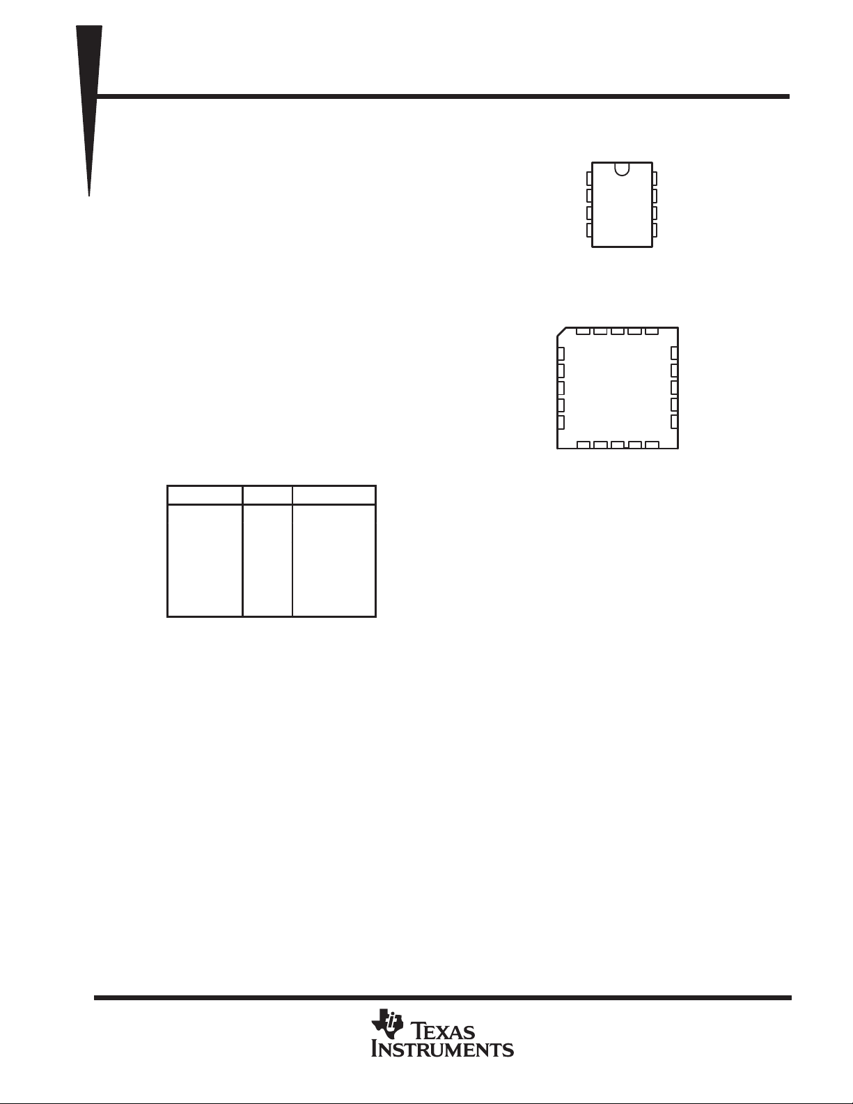
SN55461, SN55462, SN55463 . . . JG PACKAGE
SN75461, SN75462, SN75463 ...D OR P PACKAGE
SN55461, SN55462, SN55463 . . . FK PACKAGE
NC
1B
NC
1Y
NC
NC – No internal connection
(TOP VIEW)
1A
1B
1Y
GND
(TOP VIEW)
NC1ANCNCNC
3 2 1 20 19
4
5
6
7
8
910111213
NC
1
2
3
4
GND
NC
8
7
6
5
CC
V
2Y
18
17
16
15
14
V
2B
2A
2Y
CC
NC
2B
NC
2A
NC
description
These dual peripheral drivers are functionally interchangeable with SN55451B through SN55453B and
SN75451B through SN75453B peripheral drivers, but are designed for use in systems that require higher
breakdown voltages than those devices can provide at the expense of slightly slower switching speeds. Typical
applications include logic buffers, power drivers, relay drivers, lamp drivers, MOS drivers, line drivers, and
memory drivers.
The SN55461/SN75461, SN55462/SN75462, and SN55463/SN75463 are dual peripheral AND, NAND, and
OR drivers respectively (assuming positive logic), with the output of the gates internally connected to the bases
of the npn output transistors.
Series SN55461 drivers are characterized for operation over the full military temperature range of – 55°C
to 125°C. Series SN75461 drivers are characterized for operation from 0°C to 70°C.
PRODUCTION DATA information is current as of publication date.
Products conform to specifications per the terms of Texas Instruments
standard warranty. Production processing does not necessarily include
testing of all parameters.
Copyright 1995, Texas Instruments Incorporated
POST OFFICE BOX 655303 • DALLAS, TEXAS 75265
1
SN55461 THRU SN55463
Peak collector or output current (t
cle ≤ 50%, see Note 4)
500
500
mA
PACKAGE
A
UNIT
SN75461 THRU SN75463
DUAL PERIPHERAL DRIVERS
SLRS022A – DECEMBER 1976 – REVISED OCT OBER 1995
absolute maximum ratings over operating free-air temperature range (unless otherwise noted)
SN55’ SN75’ UNIT
Supply voltage, VCC (see Note 1) 7 7 V
Input voltage, V
Intermitter voltage (see Note 2) 5.5 5.5 V
Off-state output voltage, V
Continuous collector or output current (see Note 3) 400 400 mA
Continuous total power dissipation See Dissipation Rating Table
Operating free-air temperature range, T
Storage temperature range, T
Case temperature for 60 seconds, T
Lead temperature 1,6 mm (1/16 inch) from case for 60 seconds JG package 300 °C
Lead temperature 1,6 mm (1/16 inch) from case for 10 seconds D or P package 260 °C
†
Stresses beyond those listed under “absolute maximum ratings” may cause permanent damage to the device. These are stress ratings only, and
functional operation of the device at these or any other conditions beyond those indicated under “recommended operating conditions” is not
implied. Exposure to absolute-maximum-rated conditions for extended periods may affect device reliability.
NOTES: 1. Voltage values are with respect to network GND unless otherwise specified.
I
O
p
2. This is the voltage between two emitters A and B.
3. This value applies when the base-emitter resistance (RBE) is equal to or less than 500 Ω.
4. Both halves of these dual circuits may conduct rated current simultaneously; however , power dissipation averaged over a short time
interval must fall within the continuous dissipation rating.
≤ 10 ms, duty cy
w
stg
C
A
FK package 260 °C
5.5 5.5 V
35 35 V
–55 to 125 0 to 70 °C
–65 to 150 –65 to 150 °C
†
T
≤ 25°C DERATING FACTOR T
POWER RATING ABOVE TA = 25°CAPOWER RATINGAPOWER RATING
D 725 mW 5.8 mW/°C 464 mW –
FK 1375 mW 11.0 mW/°C 880 mW 275 mW
JG 1050 mW 8.4 mW/°C 672 mW 210 mW
P 1000 mW 8.0 mW/°C 640 mW –
recommended operating conditions
Supply voltage, V
High-level input voltage, V
Low-level input voltage, V
Operating free-air temperature, T
CC
IH
IL
A
DISSIPATION RATING TABLE
= 70°C T
SN55’ SN75’
MIN NOM MAX MIN NOM MAX
4.5 5 5.5 4.75 5 5.25 V
2 2 V
–55 125 0 70 °C
= 125°C
0.8 0.8 V
2
POST OFFICE BOX 655303 • DALLAS, TEXAS 75265
SN55461 THRU SN55463
PARAMETER
TEST CONDITIONS
†
UNIT
IOHHigh-level output current
CC
,
IH
,
300
100µA
CC
,
IL
,
0.25
0.5
0.25
0.4
VOLLow-level output voltage
V
CC
,
IL
,
0.5
0.8
0.5
0.7
O
,
L
,
ns
VOHHigh-level output voltage after switching
S
O
mV
SN75461 THRU SN75463
DUAL PERIPHERAL DRIVERS
SLRS022A – DECEMBER 1976 – REVISED OCT OBER 1995
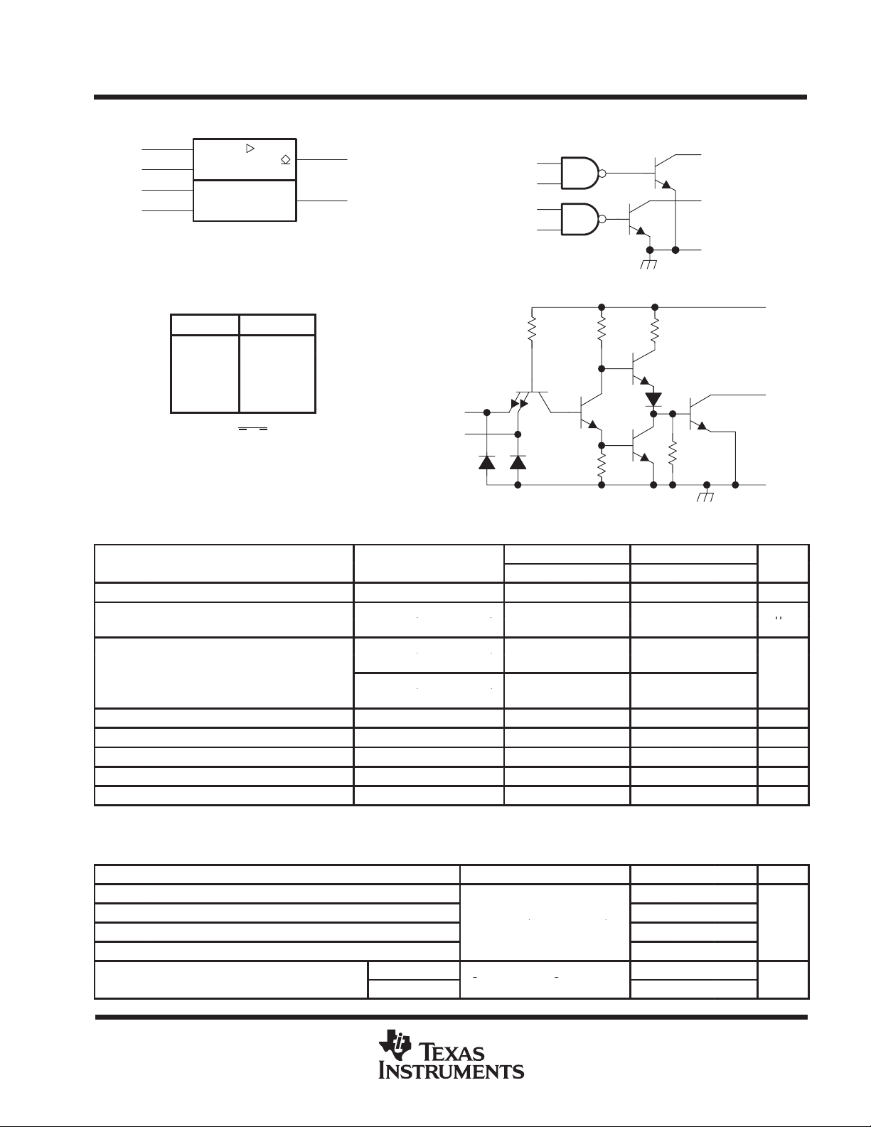
logic symbol
1
1A
2
1B
6
2A
7
2B
†
This symbol is in accordance with ANSI/IEEE Std 91-1984
and IEC Publication 617-12.
Pin numbers shown are for D, JG, and P packages.
†
&
FUNCTION TABLE
(each driver)
A
B
L L L (on state)
L H L (on state)
H L L (on state)
H H H (off state)
positive logic:
Y = AB or A
+ B
logic diagram (positive logic)
3
1Y
5
2Y
1A
1B
2A
2B
1
2
6
7
schematic (each driver)
Y
A
B
Resistor values shown are nominal.
4 kΩ 1.6 kΩ 130 Ω
500 Ω
1 kΩ
electrical characteristics over recommended operating free-air temperature range
SN55461 SN75461
MIN TYP‡MAX MIN TYP‡MAX
V
IK
I
I
I
IH
I
IL
I
CCH
I
CCL
†
For conditions shown as MIN or MAX, use the appropriate value specified under recommended operating conditions.
‡
All typical values are at VCC = 5 V, TA = 25°C.
Input clamp voltage VCC = MIN, II = –12 mA –1.2 –1.5 –1.2 –1.5 V
V
p
p
Input current at maximum input voltage VCC = MAX, VI = 5.5 V 1 1 mA
High-level input current VCC = MAX, VI = 2.4 V 40 40 µA
Low-level input current VCC = MAX, VI = 0.4 V –1 –1.6 –1 –1.6 mA
Supply current, outputs high VCC = MAX, VI = 5 V 8 11 8 11 mA
Supply current, outputs low VCC = MAX, VI = 0 56 76 56 76 mA
= MIN, V
VOH = 35 V
V
= MIN, V
IOL = 100 mA
V
= MIN, V
IOL = 300 mA
= MIN,
= 0.8 V,
= 0.8 V,
switching characteristics, VCC = 5 V, TA = 25°C
PARAMETER TEST CONDITIONS MIN TYP MAX UNIT
t
PLH
t
PHL
t
TLH
t
THL
Propagation delay time, low-to-high-level output 30 55
Propagation delay time, high-to-low-level output
Transition time, low-to-high-level output
Transition time, high-to-low-level output 10 20
p
SN55461
SN75461
I
≈ 200 mA, C
RL = 50 Ω,
VS = 30 V, IO ≈ 300 mA,
See Figure 2
= 15 pF,
See Figure 1
VS–10
VS–10
3
1Y
5
2Y
4
GND
25 40
8 20
V
CC
Y
GND
POST OFFICE BOX 655303 • DALLAS, TEXAS 75265
3

SN55461 THRU SN55463
PARAMETER
TEST CONDITIONS
†
UNIT
IOHHigh-level output current
CC
,
IL
,
300
100µA
CC
,
IH
,
0.25
0.5
0.25
0.4
VOLLow-level output voltage
V
CC
,
IH
,
0.5
0.8
0.5
0.7
O
,
L
,
ns
VOHHigh-level output voltage after switching
S
O
mV
SN75461 THRU SN75463
DUAL PERIPHERAL DRIVERS
SLRS022A – DECEMBER 1976 – REVISED OCT OBER 1995
logic symbol
1A
1B
2A
2B
†
This symbol is in accordance with ANSI/IEEE Std 91-1984
and IEC Publication 617-12.
Pin numbers shown are for D, JG, and P packages.
†
1
2
6
7
FUNCTION TABLE
(each driver)
A
B
L L H (off state)
L H H (off state)
H L H (off state)
H H L (on state)
positive logic:
Y = AB
or A + B
logic diagram (positive logic)
&
3
1Y
5
2Y
1A
1B
2A
2B
1
2
6
7
schematic (each driver)
1 kΩ
1.6 kΩ
1.6 kΩ
1 kΩ
Y
A
B
Resistor values shown are nominal.
4 kΩ
electrical characteristics over recommended operating free-air temperature range
SN55462 SN75462
MIN TYP‡MAX MIN TYP‡MAX
V
Input clamp voltage VCC = MIN, II = –12 mA –1.2 –1.5 –1.2 –1.5 V
IK
V
p
p
I
Input current at maximum input voltage VCC = MAX, VI = 5.5 V 1 1 mA
I
I
High-level input current VCC = MAX, VI = 2.4 V 40 40 µA
IH
I
Low-level input current VCC = MAX, VI = 0.4 V –1.1 –1.6 –1.1 –1.6 mA
IL
I
Supply current, outputs high VCC = MAX, VI = 0 13 17 13 17 mA
CCH
I
Supply current, outputs low VCC = MAX, VI = 5 V 61 76 61 76 mA
CCL
†
For conditions shown as MIN or MAX, use the appropriate value specified under recommended operating conditions.
‡
All typical values are at VCC = 5 V, TA = 25°C.
= MIN, V
VOH = 35 V
V
= MIN, V
IOL = 100 mA
V
= MIN, V
IOL = 300 mA
= 0.8 V,
= MIN,
= MIN,
switching characteristics, VCC = 5 V, TA = 25°C
PARAMETER TEST CONDITIONS MIN TYP MAX UNIT
t
Propagation delay time, low-to-high-level output 45 65
PLH
t
Propagation delay time, high-to-low-level output
PHL
t
Transition time, low-to-high-level output
TLH
t
Transition time, high-to-low-level output 10 20
THL
p
SN55462
SN75462
I
≈ 200 mA, C
RL = 50 Ω,
VS = 30 V, IO ≈ 300 mA,
See Figure 2
= 15 pF,
See Figure 1
VS–10
VS–10
3
1Y
5
2Y
4
GND
130 Ω
500 Ω
30 50
13 25
V
CC
Y
GND
4
POST OFFICE BOX 655303 • DALLAS, TEXAS 75265

SN55461 THRU SN55463
PARAMETER
TEST CONDITIONS
†
UNIT
IOHHigh-level output current
CC
,
IH
,
300
100µA
CC
,
IL
,
0.25
0.5
0.25
0.4
VOLLow-level output voltage
V
CC
,
IL
,
0.5
0.8
0.5
0.7
O
,
L
,
ns
VOHHigh-level output voltage after switching
S
O
mV
SN75461 THRU SN75463
DUAL PERIPHERAL DRIVERS
SLRS022A – DECEMBER 1976 – REVISED OCT OBER 1995
logic symbol
1A
1B
2A
2B
†
This symbol is in accordance with ANSI/IEEE Std 91-1984
and IEC Publication 617-12.
Pin numbers shown are for D, JG, and P packages.
†
1
2
6
7
FUNCTION TABLE
(each driver)
A
B
L L L (on state)
L H H (off state)
H L H (off state)
H H H (off state)
positive logic:
Y = A + B or A
≥1
3
1Y
5
2Y
Y
B
logic diagram (positive logic)
1
1A
2
1B
6
2A
7
2B
schematic (each driver)
4 kΩ 1.6 kΩ 130 Ω
A
B
1 kΩ
Resistor values shown are nominal.
4 kΩ
3
1Y
5
2Y
4
GND
V
CC
Y
500 Ω
GND
electrical characteristics over recommended operating free-air temperature range
SN55463 SN75463
TYP
‡
MAX MIN
TYP
MIN
V
Input clamp voltage VCC = MIN, II = –12 mA –1.2 –1.5 –1.2 –1.5 V
IK
V
p
p
I
Input current at maximum input voltage VCC = MAX, VI = 5.5 V 1 1 mA
I
I
High-level input current VCC = MAX, VI = 2.4 V 40 40 µA
IH
I
Low-level input current VCC = MAX, VI = 0.4 V –1 –1.6 –1 –1.6 mA
IL
I
Supply current, outputs high VCC = MAX, VI = 5 V 8 11 8 11 mA
CCH
I
Supply current, outputs low VCC = MAX, VI = 0 58 76 58 76 mA
CCL
†
For conditions shown as MIN or MAX, use the appropriate value specified under recommended operating conditions.
‡
All typical values are at VCC = 5 V, TA = 25°C.
= MIN, V
VOH = 35 V
V
= MIN, V
IOL = 100 mA
V
= MIN, V
IOL = 300 mA
= MIN,
= 0.8 V,
= 0.8 V,
switching characteristics, VCC = 5 V, TA = 25°C
PARAMETER TEST CONDITIONS MIN TYP MAX UNIT
t
Propagation delay time, low-to-high-level output 30 55
PLH
t
Propagation delay time, high-to-low-level output
PHL
t
Transition time, low-to-high-level output
TLH
t
Transition time, high-to-low-level output 10 25
THL
p
SN55463
SN75463
I
≈ 200 mA, C
RL = 50 Ω,
VS = 30 V, IO ≈ 300 mA,
See Figure 2
= 15 pF,
See Figure 1
VS–10
VS–10
‡
MAX
25 40
8 25
POST OFFICE BOX 655303 • DALLAS, TEXAS 75265
5
SN55461 THRU SN55463
SN75461 THRU SN75463
DUAL PERIPHERAL DRIVERS
SLRS022A – DECEMBER 1976 – REVISED OCT OBER 1995
PARAMETER MEASUREMENT INFORMATION
≤ 5 ns
2.4 VInput
’461
’462
Pulse
Generator
(see Note A)
’463
0.4 V
TEST CIRCUIT
NOTES: A. The pulse generator has the following characteristics: PRR ≤ 1 MHz, ZO ≈ 50 Ω.
B. CL includes probe and jig capacitance.
RL = 50 Ω
Circuit
Under
Test
(see Note B)
GND
SUB
10 V
Output
CL = 15 pF
(see Note B)
Input
’461
’463
≤ 5 ns ≤ 10 ns
Input
’462
t
PHL
Output
t
THL
Figure 1. Test Circuit and Voltage Waveforms for Switching Times
Pulse
Generator
(see Note A)
2.4 VInput
’461
’462
’463
5 V
1N3064
Circuit
Under
Test
(see Note B)
GND
VS = 30 V
2 mH
65 Ω
Output
CL = 15 pF
(see Note B)
SUB
≤ 5 ns
Input
’461
’463
≤ 5 ns ≤ 10 ns
Input
’462
Output
10% 10%
0.5 µs
90% 90%
1.5 V1.5 V
50% 50%
10% 10%
VOLTAGE WAVEFORMS
1.5 V1.5 V
10% 10%
40 µs
90% 90%
1.5 V1.5 V
1.5 V1.5 V
90%90%
10%10%
≤ 10 ns
90%90%
10%10%
≤ 10 ns
t
PLH
90%90%
t
TLH
3 V
0 V
3 V
0 V
V
V
3 V
0 V
3 V
0 V
V
OH
OL
OH
0.4 V
TEST CIRCUIT
NOTES: A. The pulse generator has the following characteristics: PRR ≤ 12.5 kHz, ZO = 50 Ω.
B. CL includes probe and jig capacitance.
Figure 2. Test Circuit and Voltage Waveforms for Latch-Up Test
6
POST OFFICE BOX 655303 • DALLAS, TEXAS 75265
VOLTAGE WAVEFORMS
V
OL

IMPORTANT NOTICE
T exas Instruments and its subsidiaries (TI) reserve the right to make changes to their products or to discontinue
any product or service without notice, and advise customers to obtain the latest version of relevant information
to verify, before placing orders, that information being relied on is current and complete. All products are sold
subject to the terms and conditions of sale supplied at the time of order acknowledgement, including those
pertaining to warranty, patent infringement, and limitation of liability.
TI warrants performance of its semiconductor products to the specifications applicable at the time of sale in
accordance with TI’s standard warranty. Testing and other quality control techniques are utilized to the extent
TI deems necessary to support this warranty . Specific testing of all parameters of each device is not necessarily
performed, except those mandated by government requirements.
CERTAIN APPLICATIONS USING SEMICONDUCTOR PRODUCTS MAY INVOLVE POTENTIAL RISKS OF
DEATH, PERSONAL INJURY, OR SEVERE PROPERTY OR ENVIRONMENTAL DAMAGE (“CRITICAL
APPLICATIONS”). TI SEMICONDUCTOR PRODUCTS ARE NOT DESIGNED, AUTHORIZED, OR
WARRANTED TO BE SUITABLE FOR USE IN LIFE-SUPPORT DEVICES OR SYSTEMS OR OTHER
CRITICAL APPLICA TIONS. INCLUSION OF TI PRODUCTS IN SUCH APPLICATIONS IS UNDERST OOD TO
BE FULLY AT THE CUSTOMER’S RISK.
In order to minimize risks associated with the customer’s applications, adequate design and operating
safeguards must be provided by the customer to minimize inherent or procedural hazards.
TI assumes no liability for applications assistance or customer product design. TI does not warrant or represent
that any license, either express or implied, is granted under any patent right, copyright, mask work right, or other
intellectual property right of TI covering or relating to any combination, machine, or process in which such
semiconductor products or services might be or are used. TI’s publication of information regarding any third
party’s products or services does not constitute TI’s approval, warranty or endorsement thereof.
Copyright 1998, Texas Instruments Incorporated
 Loading...