

Page 1
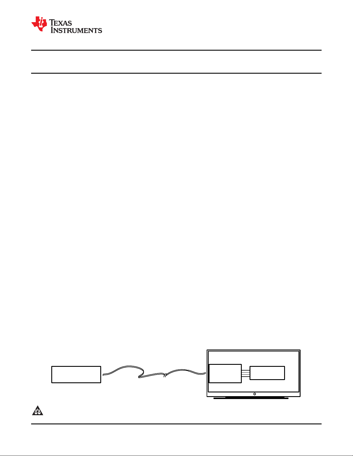
DVI / HDMI
Source
text
DS16EV5110
DeS / Display
Controller
DVI / HDMI Sink
20m 28 AWG DVI / HDMI Cable
DS16EV5110
www.ti.com
DS16EV5110 Video Equalizer (3D+C) for DVI, HDMI Sink-Side Applications
Check for Samples: DS16EV5110
1
FEATURES
2
• 8 Levels of Equalization Settable by 3 Pins or
Through the SMBus Interface
• DC-Coupled Inputs and Outputs
• Optimized for Operation From 250 Mbps to
2.25 Gbps in Support of UXGA, 480 I/P, 720 I/P, DESCRIPTION 1080 I, and 1080 P With 8, 10, and 12-Bit Color Depth Resolutions
• Two DS16EV5110 Devices Support DVI/HDMI
Dual Link
• DVI 1.0, and HDMI 1.3a Compatible TMDS
Interface
• Clock Channel Signal Detect (LOS)
• Enable for Power Savings Standby Mode
• System Management Bus (SMBus) Provides
Control of Boost, Output Amplitude, Enable,
and Clock Channel Signal Detect Threshold
• Low Power Consumption: 475mW (Typical)
• 0.13 UI Total Jitter at 1.65 Gbps Including
Cable
• Single 3.3V Power Supply
• Small 7mm x 7mm, 48-Pin Leadless WQFN
Package
• -40°C to +85°C Operating Temperature Range
• Extends TMDS Cable Reach Over:
1. > 40 Meters 24 AWG DVI Cable (1.65Gbps)
2. > 20 Meters 28 AWG DVI Cable (1.65Gbps)
3. > 20 Meters Cat5/Cat5e/Cat6 Cables
(1.65Gbps)
4. > 20 Meters 28 AWG HDMI Cables
(2.25Gbps)
APPLICATIONS
• Sink-Side Video Applications
• Projectors
• High Definition Displays
The DS16EV5110 is a multi-channel equalizer
optimized for video cable extension sink-side
applications. It operates between 250Mbps and
2.25Gbps with common applications at 1.65Gbps and
2.25Gbps (per data channel). It contains three
Transition-Minimized Differential Signaling (TMDS)
data channels and one clock channel as commonly
found in DVI and HDMI cables. It provides
compensation for skin-effect and dielectric losses, a
common phenomenon when transmitting video on
commercially available high definition video cables.
The inputs conform to DVI and HDMI requirements
and features programmable levels of input
equalization. The programmable levels of
equalization provide optimal signal boost and reduces
inter-symbol interference. Eight levels of boost are
selectable via a pin interface or by the optional
System Management Bus.
The clock channel is optimized for clock rates of up to
225 MHz and features a signal detect circuit. To
maximize noise immunity, the DS16EV5110 features
a signal detector with programmable thresholds. The
threshold is adjustable through a System
Management Bus (SMBus) interface.
The DS16EV5110 also provides support for system
power management via output enable controls.
Additional controls are provided via the SMBus
enabling customization and optimization for specific
applications requirements. These controls include
programmable features such as output amplitude and
boost controls as well as system level diagnostics.
SNLS249M –FEBRUARY 2007–REVISED APRIL 2013
Typical Application
1
2All trademarks are the property of their respective owners.
PRODUCTION DATA information is current as of publication date.
Products conform to specifications per the terms of the Texas
Instruments standard warranty. Production processing does not
necessarily include testing of all parameters.
Please be aware that an important notice concerning availability, standard warranty, and use in critical applications of
Texas Instruments semiconductor products and disclaimers thereto appears at the end of this data sheet.
Copyright © 2007–2013, Texas Instruments Incorporated
Page 2
DS16EV5110
SNLS249M –FEBRUARY 2007–REVISED APRIL 2013
www.ti.com
PIN DESCRIPTIONS
Pin Name Pin Number I/O
HIGH SPEED DIFFERENTIAL I/O
C_IN− 1 I, CML Inverting and non-inverting TMDS Clock inputs to the equalizer. An on-chip 50Ω terminating
C_IN+ 2 resistor connects C_IN+ to VDD and C_IN- to VDD.
D_IN0− 4 I, CML Inverting and non-inverting TMDS Data inputs to the equalizer. An on-chip 50Ω terminating
D_IN0+ 5 resistor connects D_IN0+ to VDD and D_IN0- to VDD.
D_IN1− 8 I, CML Inverting and non-inverting TMDS Data inputs to the equalizer. An on-chip 50Ω terminating
D_IN1+ 9 resistor connects D_IN1+ to VDD and D_IN1- to VDD.
D_IN2− 11 I, CML Inverting and non-inverting TMDS Data inputs to the equalizer. An on-chip 50Ω terminating
D_IN2+ 12 resistor connects D_IN2+ to VDD and D_IN2- to VDD.
C_OUT- 36 O, CML Inverting and non-inverting TMDS outputs from the equalizer. Open collector.
C_OUT+ 35
D_OUT0− 33 O, CML Inverting and non-inverting TMDS outputs from the equalizer. Open collector.
D_OUT0+ 32
D_OUT1– 29 O, CML Inverting and non-inverting TMDS outputs from the equalizer. Open collector.
D_OUT1+ 28
D_OUT2− 26 O, CML Inverting and non-inverting TMDS outputs from the equalizer. Open collector.
D_OUT2+ 25
Equalization Control
BST_0 23 I, LVCMOS BST_0, BST_1, and BST_2 select the equalizer boost level for EQ channels. BST_0, BST_1,
BST_1 14 and BST_2 are internally pulled Low. See Table 2.
BST_2 37
Device Control
EN 44 I, LVCMOS Enable Equalizer input. When held High, normal operation is selected. When held Low,
FEB 21 I, LVCMOS Force External Boost. When held High, the equalizer boost setting is controlled by the
SD 45 O, LVCMOS Equalizer Clock Channel Signal Detect Output. Produces a High when signal is detected.
POWER
V
DD
GND 22, 24, GND Ground reference. GND should be tied to a solid ground plane through a low impedance
Exposed Pad DAP GND The exposed pad at the center of the package must be connected to the ground plane.
System Management Bus (SMBus) Interface Control Pins
SDA 18 IO, LVCMOS SMBus Data Input / Output. Internally pulled High to 3.3V with High-Z pull up.
SDC 17 I, LVCMOS SMBus Clock Input. Internally pulled High to 3.3V with High-Z pull up.
CS 16 I, LVCMOS SMBus Chip select. When held High, the equalizer SMBus register is enabled. When held
Other
Reserv 19, 20, 38, Reserved. Do not connect.
(1) Note: I = Input,O = Output, IO =Input/Output,
3, 6, 7, Power VDDpins should be tied to the VDDplane through a low inductance path. A 0.1µF bypass
10, 13, capacitor should be connected between each VDDpin to the GND planes.
15, 46
27, 30, path.
31, 34
39, 40,41,
42, 43, 47,
48
(1)
, Type Description
standby mode is selected. EN is internally pulled High. Signal is global to all Data and Clock
channels.
BST_[0:2] pins. When held Low, the equalizer boost level is controlled through the SMBus
(see Table 1) control pins. FEB is internally pulled High.
Low, the equalizer SMBus register is disabled. CS is internally pulled Low. CS is internally
gated with SDC.
2 Submit Documentation Feedback Copyright © 2007–2013, Texas Instruments Incorporated
Product Folder Links: DS16EV5110
Page 3
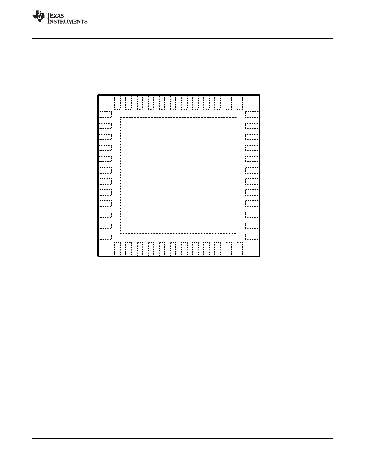
DAP = GND
DS16EV5110SQ
(Top View)
1
2
3
4
5
6
7
8
9
10
11
12
13
14
15
16
17
18
19
20
21
22
23
24
36
35
34
33
32
31
30
29
28
27
26
25
48
47
46
45
44
43
42
41
40
39
38
37
D_IN2+
D_IN2-
D_IN1+
D_IN1-
D_IN0+
D_IN0-
C_IN+
C_IN-
D_OUT2+
D_OUT2-
D_OUT1+
D_OUT1-
D_OUT0+
D_OUT0-
C_OUT+
C_OUT-
VDD
VDD
VDD
VDD GND
GND
GND
GND
VDD
VDD
GND
GND
BST_1
BST_0
CS
SDC
SDA
Reserv
VDD
SD
EN
Reserv
Reserv
Reserv
Reserv
Reserv
Reserv
Reserv
BST_2
Reserv
FEB
Reserv
DS16EV5110
www.ti.com
Connection Diagram
SNLS249M –FEBRUARY 2007–REVISED APRIL 2013
TOP VIEW — Not to Scale
Copyright © 2007–2013, Texas Instruments Incorporated Submit Documentation Feedback 3
Product Folder Links: DS16EV5110
Page 4
DS16EV5110
SNLS249M –FEBRUARY 2007–REVISED APRIL 2013
www.ti.com
These devices have limited built-in ESD protection. The leads should be shorted together or the device placed in conductive foam
during storage or handling to prevent electrostatic damage to the MOS gates.
Absolute Maximum Ratings
(1)(2)
Supply Voltage (VDD) -0.5V to +4.0V
LVCMOS Input Voltage -0.5V + 4.0V
LVCMOS Output Voltage -0.5V to 4.0V
CML Input/Output Voltage -0.5V to 4.0V
Junction Temperature +150°C
Storage Temperature -65°C to +150°C
Lead Temperature (Soldering, 5 sec.) +260°C
ESD Rating
HBM, 1.5 kΩ, 100 pF >8 kV
CML Inputs >10 kV
Thermal Resistance θJA, No Airflow 30°C/W
(1) “Absolute Maximum Ratings” indicate limits beyond which damage to the device may occur, including inoperability and degradation of
device reliability and/or performance. Functional operation of the device and/or non-degradation at the Absolute Maximum Ratings or
other conditions beyond those indicated in the Recommended Operating Conditions is not implied. The Recommended Operating
Conditions indicate conditions at which the device is functional and the device should not be operated beyond such conditions. Absolute
Maximum Numbers are ensured for a junction temperature range of –40°C to +125°C. Models are validated to Maximum Operating
Voltages only.
(2) If Military/Aerospace specified devices are required, please contact the TI Sales Office/Distributors for availability and specifications.
Recommended Operating Conditions
(1)(2)
Min Typ Max Units
Supply Voltage (VDDto GND) 3.0 3.3 3.6 V
Ambient Temperature -40 25 +85 °C
(1) Typical values represent most likely parametric norms at VDD= 3.3V, TA= 25°C, and at the Recommended Operation Conditions at the
time of product characterization and are not ensured.
(2) The Electrical Characteristics tables list ensured specifications under the listed Recommended Operating Conditions except as
otherwise modified or specified by the Electrical Characteristics Conditions and/or Notes.
Electrical Characteristics
Over recommended operating supply and temperature ranges unless other specified.
Symbol Parameter Conditions Min Typ Max Units
LVCMOS DC SPECIFICATIONS
I
IH-PU
I
IH-PD
I
IL-PU
I
IL-PD
V
IH
V
IL
V
OH
V
OL
POWER
PD Power Dissipation EN = High, Device Enabled 475 700 mW
(1) Typical values represent most likely parametric norms at VDD= 3.3V, TA= 25°C, and at the Recommended Operation Conditions at the
time of product characterization and are not ensured.
(2) The Electrical Characteristics tables list ensured specifications under the listed Recommended Operating Conditions except as
otherwise modified or specified by the Electrical Characteristics Conditions and/or Notes.
4 Submit Documentation Feedback Copyright © 2007–2013, Texas Instruments Incorporated
High Level Input Leakage Current LVCMOS pins with internal pull-up
resistors
High Level Input Leakage Current LVCMOS pins with internal pull-
down resistors
Low Level Input Leakage Current LVCMOS pins with internal pull-up
resistors
Low Level Input Leakage Current LVCMOS pins with internal pull-
down resistors
High Level Input Voltage 2.0 VDD V
Low Level Input Voltage 0 0.8 V
High Level Output Voltage SD Pin, IOH= -3mA 2.4 V
Low Level Output Voltage SD Pin, IOL= 3mA 0.4 V
EN = Low, Power Down Mode 70 mW
Product Folder Links: DS16EV5110
(1)(2)
-10 +10 μA
80 105 μA
-20 -10 μA
-10 +10 μA
Page 5
DS16EV5110
www.ti.com
SNLS249M –FEBRUARY 2007–REVISED APRIL 2013
Electrical Characteristics (continued)
Over recommended operating supply and temperature ranges unless other specified.
Symbol Parameter Conditions Min Typ Max Units
N Supply Noise Tolerance
CML INPUTS
V
TX
V
ICMDC
V
IN
R
LI
R
IN
Input Voltage Swing (Launch Measured differentially at TPA
Amplitude) (Figure 2)
Input Common-Mode Voltage DC-Coupled Requirement
Input Voltage Swing Measured differentially at TPB
Differential Input Return Loss 100 MHz– 825 MHz, with fixture's
Input Resistance IN+ to VDD and IN− to VDD 45 50 55 Ω
CML OUTPUTS
V
O
V
OCM
tR, t
t
CCSK
t
D
F
Output Voltage Swing Measured differentially with OUT+
Output common-mode Voltage Measured Single-ended VDD-0.3 VDD-0.2 V
Transition Time 20% to 80% of differential output
Inter Pair Channel-to-Channel Difference in 50% crossing
Skew (all 4 Channels) between shortest and longest 25 ps
Latency 350 ps
OUTPUT JITTER
TJ1 Total Jitter at 1.65 Gbps 20m 28 AWG STP DVI Cable
TJ2 Total Jitter at 2.25 Gbps 20m 28 AWG STP DVI Cable
TJ3 Total Jitter at 165 MHz Clock Paths
TJ4 Total Jitter at 225 MHz Clock Paths
RJ Random Jitter See
BIT RATE
F
CLK
Clock Frequency Clock Path
BR Bit Rate Data Path
(3) Allowed supply noise (mV
(4) Specification is ensured by characterization and is not tested in production.
P-P
(5) Deterministic jitter is measured at the differential outputs (TPC of Figure 2), minus the deterministic jitter before the test channel (TPA of
Figure 2). Random jitter is removed through the use of averaging or similar means.
(6) Total Jitter is defined as peak-to-peak deterministic jitter from()+ 14.2 times random jitter in ps
(7) Random jitter contributed by the equalizer is defined as sq rt (J
TPC of Figure 2; JINis the random jitter at the input of the equalizer in ps
(3)
DC to 50MHz 100 mV
Measured at TPA (Figure 2)
(Figure 2)
effect de-embedded
and OUT− terminated by 50Ω to 800 1200 mV
VDD
voltage, measured within 1" from 75 240 ps
output pins.
channels
Data Paths 0.13 0.17 UI
EQ Setting 0x04 PRBS7
Data Paths 0.2 UI
EQ Setting 0x04 PRBS7
Clock Pattern
Clock Pattern
(6) (7)
(4)
(4)
sine wave) under typical conditions.
(4) (5) (6)
(4) (5) (6)
2
OUT
(4) (5) (6)
(4) (5) (6)
2
− J
). J
IN
OUT
, see TPA of Figure 2.
rms
is the random jitter at equalizer outputs in ps
(1)(2)
800 1200 mV
VDD-0.3 VDD-0.2 V
120 mV
10 dB
0.165 UI
0.165 UI
3 ps
25 225 MHz
0.25 2.25 Gbps
.
rms
rms
, see
P-P
P-P
P-P
P-P
P-P
P-P
P-P
P-P
rms
Copyright © 2007–2013, Texas Instruments Incorporated Submit Documentation Feedback 5
Product Folder Links: DS16EV5110
Page 6
DS16EV5110
SNLS249M –FEBRUARY 2007–REVISED APRIL 2013
Electrical Characteristics — System Management Bus Interface
(1)(2)
www.ti.com
Over recommended operating supply and temperature ranges unless other specified.
Symbol Parameter Conditions Min Typ Max Units
System Bus Interface — DC Specifications
V
IL
V
IH
I
PULLUP
V
DD
I
LEAK-Bus
I
LEAK-Pin
C
I
R
TERM
System Bus Interface Timing Specification
FSMB Bus Operating Frequency See
TBUF Bus Free Time Between Stop and Start
THD:STA Hold Time After (Repeated) Start Condition. At I
TSU:STA Repeated Start Condition Setup Time 4.7 µs
TSU:STO Stop Condition Setup Time 4.0 µs
THD:DAT Data Hold Time 300 ns
TSU:DAT Data Setup Time 250 ns
T
TIMEOUT
T
LOW
T
HIGH
T
:SEXT Cumulative Clock Low Extend Time (Slave See
LOW
t
F
t
R
t
POR
Data, Clock Input Low Voltage 0.8 V
Data, Clock Input High Voltage 2.8 V
Current through pull-up resistor or current VOL = 0.4V
source
10 mA
DD
Nominal Bus Voltage 3.0 3.6 V
Input Leakage per bus segment See
(3)
—200 +200 µA
Input Leakage per device pin —15 µA
DD3.3
PULLUP
(3) (4)
(3) (4) (5)
(6)
(6)
, Max
10 pF
1000 Ω
10 100 kHz
4.7 µs
4.0 µs
25 35 ms
Capacitance for SDA and SDC See
Termination Resistance V
Condition
First CLK generated after this period.
Detect Clock Low Timeout See
Clock Low Period 4.7 µs
Clock High Period See
Device)
Clock/Data Fall Time See
Clock/Data Rise Time See
Time in which a device must be operational See
after power-on reset
(6)
(6)
(6)
(6)
(6)
4.0 50 µs
2 ms
300 ns
1000 ns
500 ms
V
(1) Typical values represent most likely parametric norms at VDD= 3.3V, TA= 25°C, and at the Recommended Operation Conditions at the
time of product characterization and are not ensured.
(2) The Electrical Characteristics tables list ensured specifications under the listed Recommended Operating Conditions except as
otherwise modified or specified by the Electrical Characteristics Conditions and/or Notes.
(3) Recommended value. Parameter not tested in production.
(4) Recommended maximum capacitance load per bus segment is 400pF.
(5) Maximum termination voltage should be identical to the device supply voltage.
(6) Compliant to SMBus 2.0 physical layer specification. See System Management Bus (SMBus) Specification Version 2.0, section 3.1.1
SMBus common AC specifications for details.
6 Submit Documentation Feedback Copyright © 2007–2013, Texas Instruments Incorporated
Product Folder Links: DS16EV5110
Page 7
Pattern Generator
100 mV
PP
Differential
SMA to HDMI Adapter
DS
16
EV
5110
SMA to HDMI Adapter
Jitter Test Instrument
Coax
SMA
Coax
SMA
Coax
SMA
Coax
SMA
Coax
SMA
Coax
SMA
Coax
SMA
VDD
RLoadRLoad
VDD
RLoadRLoad
VDD
RLoadRLoad
RLoadRLoad
Coax
SMA
VDD
RLoadRLoad
VDD
RLoadRLoad
VDD
RLoadRLoad
VDD
RLoadRLoad
28 AWG
DVI/HDMI
Cable
VDD
TPCTPBTPA
SMA
SMA
SMA
SMA
SMA
SMA
SMA
SMA
Coax
Coax
Coax
Coax
Coax
Coax
Coax
Coax
ClkClk+
Data0Data0+
Data1Data1+
Data2Data2+
SP
t
BUF
t
HD:STA
t
LOW
t
R
t
HD:DAT
t
HIGH
t
F
t
SU:DAT
t
SU:STA
ST
SP
t
SU:STO
SDC
SDA
CS
t
SU:CS
ST
DS16EV5110
www.ti.com
SNLS249M –FEBRUARY 2007–REVISED APRIL 2013
TIMING DIAGRAMS
Figure 1. SMBus Timing Diagram
Figure 2. Test Setup Diagram for Jitter Measurement
Copyright © 2007–2013, Texas Instruments Incorporated Submit Documentation Feedback 7
Product Folder Links: DS16EV5110
Page 8

DS16EV5110
SNLS249M –FEBRUARY 2007–REVISED APRIL 2013
www.ti.com
SYSTEM MANAGEMENT BUS (SMBUS) AND CONFIGURATION REGISTERS
The System Management Bus interface is compatible to SMBus 2.0 physical layer specification. The use of the
Chip Select signal is required. Holding the CS pin High enables the SMBus port allowing access to the
configuration registers. Holding the CS pin Low disables the device's SMBus allowing communication from the
host to other slave devices on the bus. In the STANDBY state, the System Management Bus remains active.
When communication to other devices on the SMBus is active, the CS signal for the DS16EV5110s must be
driven Low.
The address byte for all DS16EV5110s is AC'h. Based on the SMBus 2.0 specification, the DS16EV5110 has a
7-bit slave address of 1010110'b. The LSB is set to 0'b (for a WRITE), thus the 8-bit value is 1010 1100 'b or
AC'h.
The SDC and SDA pins are 3.3V LVCMOS signaling and include high-Z internal pull up resistors. External low
impedance pull up resistors maybe required depending upon SMBus loading and speed. Note, these pins are not
5V tolerant.
Transfer of Data via the SMBus
During normal operation the data on SDA must be stable during the time when SDC is High.
There are three unique states for the SMBus:
START: A High-to-Low transition on SDA while SDC is High indicates a message START condition.
STOP: A Low-to-High transition on SDA while SDC is High indicates a message STOP condition.
IDLE: If SDC and SDA are both High for a time exceeding t
are High for a total exceeding the maximum specification for t
SMBus Transactions
The device supports WRITE and READ transactions. See Register Description table for register address, type
(Read/Write, Read Only), default value and function information.
Writing a Register
To write a register, the following protocol is used (see SMBus 2.0 specification).
1. The Host (Master) selects the device by driving its SMBus Chip Select (CS) signal High.
2. The Host drives a START condition, the 7-bit SMBus address, and a “0” indicating a WRITE.
3. The Device (Slave) drives the ACK bit (“0”).
4. The Host drives the 8-bit Register Address.
5. The Device drives an ACK bit (“0”).
6. The Host drive the 8-bit data byte.
7. The Device drives an ACK bit (“0”).
8. The Host drives a STOP condition.
9. The Host de-selects the device by driving its SMBus CS signal Low.
The WRITE transaction is completed, the bus goes IDLE and communication with other SMBus devices may
now occur.
Reading a Register
To read a register, the following protocol is used (see SMBus 2.0 specification).
1. The Host (Master) selects the device by driving its SMBus Chip Select (CS) signal High.
2. The Host drives a START condition, the 7-bit SMBus address, and a “0” indicating a WRITE.
3. The Device (Slave) drives the ACK bit (“0”).
4. The Host drives the 8-bit Register Address.
5. The Device drives an ACK bit (“0”).
6. The Host drives a START condition.
7. The Host drives the 7-bit SMBus Address, and a “1” indicating a READ.
8. The Device drives an ACK bit “0”.
8 Submit Documentation Feedback Copyright © 2007–2013, Texas Instruments Incorporated
Product Folder Links: DS16EV5110
from the last detected STOP condition or if they
BUF
then the bus will transfer to the IDLE state.
HIGH
Page 9

DS16EV5110
www.ti.com
SNLS249M –FEBRUARY 2007–REVISED APRIL 2013
9. The Device drives the 8-bit data value (register contents).
10. The Host drives a NACK bit “1”indicating end of the READ transfer.
11. The Host drives a STOP condition.
12. The Host de-selects the device by driving its SMBus CS signal Low.
The READ transaction is completed, the bus goes IDLE and communication with other SMBus devices may now
occur.
See Table 1 for more information.
Table 1. SMBus Register Descriptions
Name Address Default Type Bit 7 Bit 6 Bit 5 Bit 4 Bit 3 Bit 2 Bit 1 Bit 0
Status 0x00 0x00 RO ID Revision Reserved Reserved Reserved SD
Status 0x01 0x00 RO Reserved Boost 1 EN Reserved
Status 0x02 0x00 RO Reserved Boost 3 Reserved Boost 2
Internal 0x03 0x77 RW EN (Int.) Boost Control EN (Int.) Reserved
Enable/ 0:Enable (BC for CH0) 0:Enable
Individual 1:Disable 000 (Min Boost) 1:Disable
Channel (D_IN0±) 001 (C_IN±)
Boost 010
Control 011
for 100
C_IN±, 101
D_IN0± 110
111 (Max Boost)
Individual 0x04 0x77 RW EN (Int.) Boost Control EN (Int.) Boost Control
Channel 0:Enable (BC for CH2) 0:Enable (BC for CH1)
Boost 1:Disable 000 (Min Boost) 1:Disable 000 (Min Boost)
Control (D_IN2±) 001 (D_IN1±) 001
for 010 010
D_IN1±, 011 011
D_IN2± 100 100
101 101
110 110
111 (Max Boost) 111 (Max Boost)
Signal 0x05 0x00 RW Reserved Threshold (mV)
Detect ON
(SD_ON)
Signal 0x06 0x00 RW Reserved Threshold (mV)
Detect OFF
(SD_OFF)
SMBus 0x07 0x00 RW Reserved SMBus
orCMOS Enable
Control for 0: Disable
EN 1: Enable
Output 0x08 0x78 RW Reserved Output Level: Reserved
Level 00: 540 mVp-p
(1) Note: RO = Read Only, RW = Read/Write
(1)
00: 70 (Default)
01: 55
10: 90
11: 75
00: 40 (Default)
01: 30
10: 55
11: 45
01: 770 mVp-p
10: 1000 mVp-p
11: 1200 mVp-p
Copyright © 2007–2013, Texas Instruments Incorporated Submit Documentation Feedback 9
Product Folder Links: DS16EV5110
Page 10

DS16EV5110
SNLS249M –FEBRUARY 2007–REVISED APRIL 2013
www.ti.com
DS16EV5110 DEVICE DESCRIPTION
The DS16EV5110 video equalizer comprises three data channels, a clock channel, and a control interface
including a Systeml Management Bus (SMBus) port.
DATA CHANNELS
The DS16EV5110 provides three data channels. Each data channel consists of an equalizer stage, a limiting
amplifier, a DC offset correction block, and a TMDS driver as shown in Figure 3.
EQUALIZER BOOST CONTROL
The data channel equalizers support eight programmable levels of equalization boost. The state of the FEB pin
determines how the boost settings are controlled. If the FEB pin is held High, then the equalizer boost setting is
controlled by the Boost Set pins (BST_[0:2]) in accordance with Table 2. If this programming method is chosen,
then the boost setting selected on the Boost Set pins is applied to all three data channels. When the FEB pin is
held Low, the equalizer boost level is controlled through the SMBus. This programming method is accessed via
the appropriate SMBus registers (see Table 1). Using this approach, equalizer boost settings can be
programmed for each channel individually. FEB is internally pulled High (default setting); therefore if left
unconnected, the boost settings are controlled by the Boost Set pins (BST_[0:2]). The range of boost settings
provided enables the DS16EV5110 to address a wide range of transmission line path loss scenarios, enabling
support for a variety of data rates and formats.
Table 2. EQ Boost Control Table
Control Via SMBus Control Via Pins EQ Boost Setting at
BC_2, BC_1, BC_0 BST_2, BST_1, 825 MHz (dB)
(FEB = 0) BST_0 (TYP)
000 000 9
001 001 14
010 010 18
011 011 21
100 100 24
101 101 26
110 110 28
111 111 30
(FEB = 1)
DEVICE STATE AND ENABLE CONTROL
The DS16EV5110 has an Enable feature which provides the ability to control device power consumption. This
feature can be controlled either via the Enable Pin (EN Pin) or via the Enable Control Bit which is accessed
through the SMBus port (see Table 1 and Table 3). If Enable is activated, the data channels and clock channel
are placed in the ACTIVE state and all device blocks function as described. The DS16EV5110 can also be
placed in STANDBY mode to save power. In this mode only the control interface including the SMBus port as
well as the clock channel signal detection circuit remain active.
Table 3. Enable and Device State Control
Register 07[0] EN Pin Register 03[3] (EN Device State
(SMBus) (CMOS) Control)
0 : Disable 1 X ACTIVE
0 : Disable 0 X STANDBY
1 : Enable X 0 ACTIVE
1 : Enable X 1 STANDBY
10 Submit Documentation Feedback Copyright© 2007–2013, Texas Instruments Incorporated
Product Folder Links: DS16EV5110
(SMBus)
Page 11

Input
Termination
Equalizer
Limiting
Amplifier
DC Offset Correction
Data Channel
(0-2)
Boost Setting
3
3
3
BST_0 : BST_2
BST
CNTL
EN
EN
EN
FEB
SMBus Reg.
REG3[7],
REG4[7],
REG4[3]
EN
SMBus Register
D_OUT+
D_OUT-
D_IN+
D_IN-
SMBus Reg.
REG7[0]
DS16EV5110
www.ti.com
SNLS249M –FEBRUARY 2007–REVISED APRIL 2013
CLOCK CHANNEL
The clock channel incorporates a limiting amplifier, a DC offset correction, and a TMDS driver as shown in
Figure 4.
CLOCK CHANNEL SIGNAL DETECT
The DS16EV5110 features a signal detect circuit on the clock channel. The status of the clock signal can be
determined by either reading the Signal Detect bit (SD) in the SMBus registers (see Table 1) or by the state of
the SD pin. A logic High indicates the presence of a signal that has exceeded a specified threshold value (called
SD_ON). A logic Low means that the clock signal has fallen below a threshold value (called SD_OFF). These
values are programmed via the SMBus (Table 1). If not programmed via the SMBus, the thresholds take on the
default values for the SD_OFF and SD_ON values as indicated in Table 4. The Signal Detect threshold values
can be changed through the SMBus. All threshold values specified are DC peak-to-peak differential signals
(positive signal minus negative signal) at the input of the device.
Table 4. Clock Channel Signal Detect Threshold
Values
Bit 1 Bit 0 SD_OFF Threshold SD_ON Threshold
0 0 40 (Default) 70 (Default)
0 1 30 55
1 0 55 90
1 1 45 75
Register 06 (mV) Register 05 (mV)
Figure 3. DS16EV5110 Data Channel
Copyright © 2007–2013, Texas Instruments Incorporated Submit Documentation Feedback 11
Product Folder Links: DS16EV5110
Page 12

Input
Termination
Limiting
Amplifier
DC Offset Correction
Clock
Channel
EN
SMBus
REG3[3]
EN
EN
Signal Detect Thresh.
SMBus Register
Signal Detect
SMBus Register
SD
C_OUT-
C_OUT+
C_IN-
C_IN+
SMBus
REG7[0]
DS16EV5110
SNLS249M –FEBRUARY 2007–REVISED APRIL 2013
www.ti.com
Figure 4. DS16EV5110 Clock Channel
OUTPUT LEVEL CONTROL
The output amplitude of the TMDS drivers for both the data channels and the clock channel can be controlled via
the SMBus (see Table 1). The default output level is 1000mV p-p. The following Table presents the output level
values supported:
Table 5. Output Level Control Settings – REG
0x08[3:2]
Bit 3 Bit 2 Output Level (mV)
0 0 540
0 1 770
1 0 1000 (default)
1 1 1200
AUTOMATIC ENABLE FEATURE
It may be desired for the DS16EV5110 to be configured to automatically enter STANDBY mode if no clock signal
is present. STANDBY mode can be implemented by connecting the Signal Detect (SD) pin to the external
(LVCMOS) Enable (EN) pin. In order for this option to function properly, REG07[0] should be set to a “0” (default
value). If the clock signal applied to the clock channel input swings above the SD_ON threshold specified in the
threshold register via the SMBus, then the SD pin is asserted High. If the SD pin is connected to the EN pin, this
will enable the equalizer, limiting amplifier, and output buffer on the data channels and the limiting amplifier and
output buffer on the clock channel; thus the DS16EV5110 will automatically enter the ACTIVE state. If the clock
signal present falls below SD_OFF threshold specified in the threshold register, then the SD pin will be asserted
Low, causing the aforementioned blocks to be placed in the STANDBY state.
12 Submit Documentation Feedback Copyright© 2007–2013, Texas Instruments Incorporated
Product Folder Links: DS16EV5110
Page 13

DS16EV5110DS16EV5110
20m DVI/HDMI
Cable
HDTV
DVI/HDMI
DVD
Player
DVI/HDMI Extender
To HDTV
20m DVI/HDMI
Cable
Data 2 OUT +/-
Data 1 OUT +/-
Data 0 OUT +/-
Clock OUT +/-
Data 1 IN +/-
Data 0 IN +/-
Clock IN +/-
Data 2 IN +/-
DVI/HDMI
Extender
DS16EV5110
DVI / HDMI Source
(e.g. DVD Player)
DS16EV5110
DeS / Display
Controller
DVI / HDMI Sink
(e.g. HDTV)
20m 28 AWG DVI / HDMI Cable
DS16EV5110
www.ti.com
SNLS249M –FEBRUARY 2007–REVISED APRIL 2013
APPLICATION INFORMATION
The DS16EV5110 is used to recondition DVI/HDMI video signals or differential signals with similar characteristics
after signal loss and degradation due to transmission through a length of shielded or unshielded cable. It is
intended to be used on the Sink-side of the video link. The DS16EV5110A maybe used on the Source or Sink
side of the application. The DS16EV5110 ESD protection circuitry will not support the V
the dowstream device (e.g. DES) is powered ON and the DS16EV5110 is powered OFF. Figure 10 shows the
CML output circuitry and the ESD protection diode (current path). It is also not recommneded to enable the
DS16EV5110 CML outputs without a load attached.
Figure 5. DS16EV5110 Sink-side application
The DS16EV5110 may also be used in certain Source-side application with certain restrictions. The
DS16EV5110 CML outputs will not meet the VOFF parameter required by the HDMI Compliance Test
Specification (v1.3b) when the DS16EV5110 is powered off and the sink device is powered on. A current path
will be enabled through the ESD protection diode (see Figure 10). If full compliance is not required, the
DS16EV5110 may be used in repeater type application as shown in Figure 6.
specification when
OFF
DVI 1.0 AND HDMI V1.2a APPLICATIONS
A single DS16EV5110 can be used to implement cable extension solutions with various resolutions and screen
refresh rates. The range of digital serial rates supported is between 250 Mbps and 1.65 Gbps. For applications
requiring ultra-high resolution for DVI applications (e.g., QXGA and WQXGA), a “dual link” TMDS interface is
required. This is easily configured by using two DS16EV5110 devices as shown in Figure 7.
Copyright © 2007–2013, Texas Instruments Incorporated Submit Documentation Feedback 13
Figure 6. DS16EV5110 Repeater Application with CAT 5 cable
Product Folder Links: DS16EV5110
Page 14

DS16EV5110
DS16EV5110
D0
D1
D2
CLK
D3
D4
D5
D0
D1
D2
CLK
D3
D4
D5
CLK CLK
SD
SD
EN
EN
CS
CS
DS16EV5110
SNLS249M –FEBRUARY 2007–REVISED APRIL 2013
www.ti.com
Note the recommended connections between LVCMOS control pins. This provides the Automatic Enable feature
for both devices based on the one active clock channel. In many applications the SMBus is not required (device
is pin controlled), for this application simply leave the three SMBus pins open. SDC and SDA are internally pulled
High, and CS is internally pulled Low, thus the SMBus is in the disabled state.
Figure 7. Connection in Dual Link Application
HDMI V1.3 APPLICATION
The DS16EV5110 can reliably extend operation to distances greater than 20 meters of 28 AWG HDMI cable at
2.25 Gbps, thereby supporting HDMI v1.3 for 1080p HDTV resolution with 12-bit color depth. Please note that
the Electrical Characteristics specified in this document have not been tested for and are not ensured for 2.25
Gbps operation.
DC COUPLED DATA PATHS AND DVI/HDMI COMPLIANCE
The DS16EV5110 is designed to support TMDS differential pairs with DC coupled transmission lines. It contains
integrated termination resistors (50Ω), pulled up to VDD at the input stage, and open collector outputs for DVI /
HDMI for signal swing.
CABLE SELECTION
At higher frequencies, longer cable lengths produce greater losses due to the skin effect. The quality of the cable
with respect to conductor wire gauge and shielding heavily influences performance. Thicker conductors have
lower signal degradation per unit length. In nearly all applications, the DS16EV5110 equalization can be set to
0x04, and equalize up to 22 dB skin effect loss for all input cable configurations at all data rates, without
degrading signal integrity.
14 Submit Documentation Feedback Copyright© 2007–2013, Texas Instruments Incorporated
Product Folder Links: DS16EV5110
Page 15

5 10 15 20 25 30 35
28 AWG DVI/HDMI CABLE LENGTH (m)
0
0.1
0.2
0.3
0.4
0.5
TOTAL JITTER (
UI)
0
2.25 Gbps
1.65 Gbps
0.75 Gbps
0.25 Gbps
Unequalized
Equalized
DS16EV5110
www.ti.com
SNLS249M –FEBRUARY 2007–REVISED APRIL 2013
28 AWG STP DVI / HDMI CABLES RECOMMENDED BOOST SETTINGS
The following table presents the recommended boost control settings for various data rates and cable lengths for
28 AWG DVI/HDMI compliant configurations. Boost setting maybe done via the three BST[2:0] pins or via the
respective register values.
Table 6. Boost Control Setting for STP Cables
Setting Data Rate 28 AWG DVI / HDMI
0x04 750 Mbps 0–25m
0x04 1.65 Gbps 0–20m
0x06 750 Mbps 25m to greater than 30m
0x06 1.65 Gbps 20m to greater than 25m
0x03 2.25 Gbps 0–15m
0x06 2.25 Gbps 15m to greater than 20m
Figure 8 shows the cable extension and jitter reduction obtained with the use of the equalizer. Table 6 lists the
various gain settings used versus cable length recommendations.
Figure 8. Equalized vs. Unequalized Jitter Performance Over 28 AWG DVI/HDMI Cable
UTP (UNSHIELDED TWIST PAIRS) CABLES
The DS16EV5110 can be used to extend the length of UTP cables, such as Cat5, Cat5e and Cat6 to distances
greater than 20 meters at 1.65 Gbps with < 0.13 UI of jitter. Please note that for non-standard DVI/HDMI cables,
the user must ensure the clock-to-data channel skew requirements are met. Table 7 presents the recommended
boost control settings for various data rates and cable lengths for UTP configurations:
Copyright © 2007–2013, Texas Instruments Incorporated Submit Documentation Feedback 15
Table 7. Boost Control Setting for UTP Cables
Setting Data Rate Cat5 Cable
0x03 750 Mbps 0–25m
0x06 750 Mbps 25–45m
0x03 1.65 Gbps Greater than 20m
Product Folder Links: DS16EV5110
Page 16

0 5 10 15 20 25 30 35 40
CAT 5 CABLE LENGTH (m)
TOTAL JITTER (UI)
0
0.1
0.2
0.3
0.4
0.5
1.30 Gbps
0.75 Gbps
1.65 Gbps
Unequalized
Equalized
DS16EV5110
SNLS249M –FEBRUARY 2007–REVISED APRIL 2013
www.ti.com
Figure 9 shows the cable extension and jitter reduction obtained with the use of the equalizer. Table 7 lists the
various gain settings used versus cable length recommendations.
Figure 9. Equalized vs. Unequalized Jitter Performance Over Cat5 Cable
General Recommendations
The DS16EV5110 is a high performance circuit capable of delivering excellent performance. Careful attention
must be paid to the details associated with high-speed design as well as providing a clean power supply. Refer
to the LVDS Owner’s Manual for more detailed information on high-speed design tips as well as many other
available resources available addressing signal integrity design issues.
PCB LAYOUT CONSIDERATIONS FOR DIFFERENTIAL PAIRS
The TMDS differential inputs and outputs must have a controlled differential impedance of 100Ω. It is preferable
to route TMDS lines exclusively on one layer of the board, particularly for the input traces. The use of vias should
be avoided if possible. If vias must be used, they should be used sparingly and must be placed symmetrically for
each side of a given differential pair. Route the TMDS signals away from other signals and noise sources on the
printed circuit board. All traces of TMDS differential inputs and outputs must be equal in length to minimize intrapair skew.
WQFN FOOTPRINT RECOMMENDATIONS
See application note AN-1187 (SNOA401) for additional information on WQFN packages footprint and soldering
information.
POWER SUPPLY BYPASSING
Two approaches are recommended to ensure that the DS16EV5110 is provided with an adequate power supply.
First, the supply (VDD) and ground (GND) pins should be connected to power planes routed on adjacent layers
of the printed circuit board. The layer thickness of the dielectric should be minimized so that the VDD and GND
planes create a low inductance supply with distributed capacitance. Second, careful attention to supply
bypassing through the proper use of bypass capacitors is required. A 0.1µF bypass capacitor should be
connected to each VDD pin such that the capacitor is placed as close as possible to the DS16EV5110. Smaller
body size capacitors can help facilitate proper component placement. Additionally, three capacitors with
capacitance in the range of 2.2µF to 10µF should be incorporated in the power supply bypassing design as well.
These capacitors can be either tantalum or an ultra-low ESR ceramic and should be placed as close as possible
to the DS16EV5110.
EQUIVALENT I/O STRUCTURES
Figure 10 shows the DS16EV5110 CML output structure and ESD protection circuitry.
Figure 11 shows the DS16EV5110 CML input structure and ESD protection circuitry.
16 Submit Documentation Feedback Copyright© 2007–2013, Texas Instruments Incorporated
Product Folder Links: DS16EV5110
Page 17

50:
IN+
VDD
50:
IN-
VDD
OUT+
OUT-
DS16EV5110
www.ti.com
SNLS249M –FEBRUARY 2007–REVISED APRIL 2013
Figure 10. Equivalent Output Structure
Figure 11. Equivalent Input Structure
Copyright © 2007–2013, Texas Instruments Incorporated Submit Documentation Feedback 17
Product Folder Links: DS16EV5110
Page 18

DS16EV5110
SNLS249M –FEBRUARY 2007–REVISED APRIL 2013
www.ti.com
Typical Performance Characteristics
Figure 12. Un-equalized vs. Equalized Signal after 25m of 28 AWG DVI Cable at 1.65 Gbps (0x06 Setting)
Figure 13. Output Signal after 20m of Cat5 Cable at Figure 14. Output Signal after 30m of 28 AWG DVI Cable at
Figure 15. Output Signal after 0.3m of 28 AWG DVI Cable at Figure 16. Output Signal after 20m of 28 AWG HDMI Cable
18 Submit Documentation Feedback Copyright© 2007–2013, Texas Instruments Incorporated
1.65 Gbps (0x06 Setting) 750 Mbps (0x06 Setting)
1.65 Gbps (0x04 Setting) at 2.25 Gbps (0x06 Setting)
Product Folder Links: DS16EV5110
Page 19

DS16EV5110
www.ti.com
SNLS249M –FEBRUARY 2007–REVISED APRIL 2013
REVISION HISTORY
Changes from Revision L (April 2013) to Revision M Page
• Changed layout of National Data Sheet to TI format .......................................................................................................... 18
Copyright © 2007–2013, Texas Instruments Incorporated Submit Documentation Feedback 19
Product Folder Links: DS16EV5110
Page 20

PACKAGE OPTION ADDENDUM
www.ti.com
12-Apr-2013
PACKAGING INFORMATION
Orderable Device Status
DS16EV5110SQ/NOPB ACTIVE WQFN NJU 48 250 Green (RoHS
DS16EV5110SQX/NOPB ACTIVE WQFN NJU 48 2500 Green (RoHS
(1)
The marketing status values are defined as follows:
ACTIVE: Product device recommended for new designs.
LIFEBUY: TI has announced that the device will be discontinued, and a lifetime-buy period is in effect.
NRND: Not recommended for new designs. Device is in production to support existing customers, but TI does not recommend using this part in a new design.
PREVIEW: Device has been announced but is not in production. Samples may or may not be available.
OBSOLETE: TI has discontinued the production of the device.
Package Type Package
(1)
Drawing
Pins Package
Qty
Eco Plan
(2)
& no Sb/Br)
& no Sb/Br)
Lead/Ball Finish MSL Peak Temp
(3)
CU SN Level-3-260C-168 HR -40 to 85 DS16EV511
CU SN Level-3-260C-168 HR -40 to 85 DS16EV511
Op Temp (°C) Top-Side Markings
(4)
(2)
Eco Plan - The planned eco-friendly classification: Pb-Free (RoHS), Pb-Free (RoHS Exempt), or Green (RoHS & no Sb/Br) - please check http://www.ti.com/productcontent for the latest availability
information and additional product content details.
TBD: The Pb-Free/Green conversion plan has not been defined.
Pb-Free (RoHS): TI's terms "Lead-Free" or "Pb-Free" mean semiconductor products that are compatible with the current RoHS requirements for all 6 substances, including the requirement that
lead not exceed 0.1% by weight in homogeneous materials. Where designed to be soldered at high temperatures, TI Pb-Free products are suitable for use in specified lead-free processes.
Pb-Free (RoHS Exempt): This component has a RoHS exemption for either 1) lead-based flip-chip solder bumps used between the die and package, or 2) lead-based die adhesive used between
the die and leadframe. The component is otherwise considered Pb-Free (RoHS compatible) as defined above.
Green (RoHS & no Sb/Br): TI defines "Green" to mean Pb-Free (RoHS compatible), and free of Bromine (Br) and Antimony (Sb) based flame retardants (Br or Sb do not exceed 0.1% by weight
in homogeneous material)
(3)
MSL, Peak Temp. -- The Moisture Sensitivity Level rating according to the JEDEC industry standard classifications, and peak solder temperature.
(4)
Multiple Top-Side Markings will be inside parentheses. Only one Top-Side Marking contained in parentheses and separated by a "~" will appear on a device. If a line is indented then it is a
continuation of the previous line and the two combined represent the entire Top-Side Marking for that device.
Important Information and Disclaimer:The information provided on this page represents TI's knowledge and belief as of the date that it is provided. TI bases its knowledge and belief on information
provided by third parties, and makes no representation or warranty as to the accuracy of such information. Efforts are underway to better integrate information from third parties. TI has taken and
continues to take reasonable steps to provide representative and accurate information but may not have conducted destructive testing or chemical analysis on incoming materials and chemicals.
TI and TI suppliers consider certain information to be proprietary, and thus CAS numbers and other limited information may not be available for release.
In no event shall TI's liability arising out of such information exceed the total purchase price of the TI part(s) at issue in this document sold by TI to Customer on an annual basis.
Samples
Addendum-Page 1
Page 21

PACKAGE MATERIALS INFORMATION
www.ti.com 12-Feb-2015
TAPE AND REEL INFORMATION
*All dimensions are nominal
Device Package
DS16EV5110SQ/NOPB WQFN NJU 48 250 178.0 16.4 7.3 7.3 1.3 12.0 16.0 Q1
DS16EV5110SQX/NOPB WQFN NJU 48 2500 330.0 16.4 7.3 7.3 1.3 12.0 16.0 Q1
Type
Package
Drawing
Pins SPQ Reel
Diameter
(mm)
Reel
Width
W1 (mm)
A0
(mm)B0(mm)K0(mm)P1(mm)W(mm)
Quadrant
Pin1
Pack Materials-Page 1
Page 22

PACKAGE MATERIALS INFORMATION
www.ti.com 12-Feb-2015
*All dimensions are nominal
Device Package Type Package Drawing Pins SPQ Length (mm) Width (mm) Height (mm)
DS16EV5110SQ/NOPB WQFN NJU 48 250 213.0 191.0 55.0
DS16EV5110SQX/NOPB WQFN NJU 48 2500 367.0 367.0 38.0
Pack Materials-Page 2
Page 23

NJU0048D
MECHANICAL DATA
www.ti.com
SQA48D (Rev A)
Page 24

IMPORTANT NOTICE
Texas Instruments Incorporated and its subsidiaries (TI) reserve the right to make corrections, enhancements, improvements and other
changes to its semiconductor products and services per JESD46, latest issue, and to discontinue any product or service per JESD48, latest
issue. Buyers should obtain the latest relevant information before placing orders and should verify that such information is current and
complete. All semiconductor products (also referred to herein as “components”) are sold subject to TI’s terms and conditions of sale
supplied at the time of order acknowledgment.
TI warrants performance of its components to the specifications applicable at the time of sale, in accordance with the warranty in TI’s terms
and conditions of sale of semiconductor products. Testing and other quality control techniques are used to the extent TI deems necessary
to support this warranty. Except where mandated by applicable law, testing of all parameters of each component is not necessarily
performed.
TI assumes no liability for applications assistance or the design of Buyers’ products. Buyers are responsible for their products and
applications using TI components. To minimize the risks associated with Buyers’ products and applications, Buyers should provide
adequate design and operating safeguards.
TI does not warrant or represent that any license, either express or implied, is granted under any patent right, copyright, mask work right, or
other intellectual property right relating to any combination, machine, or process in which TI components or services are used. Information
published by TI regarding third-party products or services does not constitute a license to use such products or services or a warranty or
endorsement thereof. Use of such information may require a license from a third party under the patents or other intellectual property of the
third party, or a license from TI under the patents or other intellectual property of TI.
Reproduction of significant portions of TI information in TI data books or data sheets is permissible only if reproduction is without alteration
and is accompanied by all associated warranties, conditions, limitations, and notices. TI is not responsible or liable for such altered
documentation. Information of third parties may be subject to additional restrictions.
Resale of TI components or services with statements different from or beyond the parameters stated by TI for that component or service
voids all express and any implied warranties for the associated TI component or service and is an unfair and deceptive business practice.
TI is not responsible or liable for any such statements.
Buyer acknowledges and agrees that it is solely responsible for compliance with all legal, regulatory and safety-related requirements
concerning its products, and any use of TI components in its applications, notwithstanding any applications-related information or support
that may be provided by TI. Buyer represents and agrees that it has all the necessary expertise to create and implement safeguards which
anticipate dangerous consequences of failures, monitor failures and their consequences, lessen the likelihood of failures that might cause
harm and take appropriate remedial actions. Buyer will fully indemnify TI and its representatives against any damages arising out of the use
of any TI components in safety-critical applications.
In some cases, TI components may be promoted specifically to facilitate safety-related applications. With such components, TI’s goal is to
help enable customers to design and create their own end-product solutions that meet applicable functional safety standards and
requirements. Nonetheless, such components are subject to these terms.
No TI components are authorized for use in FDA Class III (or similar life-critical medical equipment) unless authorized officers of the parties
have executed a special agreement specifically governing such use.
Only those TI components which TI has specifically designated as military grade or “enhanced plastic” are designed and intended for use in
military/aerospace applications or environments. Buyer acknowledges and agrees that any military or aerospace use of TI components
which have not been so designated is solely at the Buyer's risk, and that Buyer is solely responsible for compliance with all legal and
regulatory requirements in connection with such use.
TI has specifically designated certain components as meeting ISO/TS16949 requirements, mainly for automotive use. In any case of use of
non-designated products, TI will not be responsible for any failure to meet ISO/TS16949.
Products Applications
Audio www.ti.com/audio Automotive and Transportation www.ti.com/automotive
Amplifiers amplifier.ti.com Communications and Telecom www.ti.com/communications
Data Converters dataconverter.ti.com Computers and Peripherals www.ti.com/computers
DLP® Products www.dlp.com Consumer Electronics www.ti.com/consumer-apps
DSP dsp.ti.com Energy and Lighting www.ti.com/energy
Clocks and Timers www.ti.com/clocks Industrial www.ti.com/industrial
Interface interface.ti.com Medical www.ti.com/medical
Logic logic.ti.com Security www.ti.com/security
Power Mgmt power.ti.com Space, Avionics and Defense www.ti.com/space-avionics-defense
Microcontrollers microcontroller.ti.com Video and Imaging www.ti.com/video
RFID www.ti-rfid.com
OMAP Applications Processors www.ti.com/omap TI E2E Community e2e.ti.com
Wireless Connectivity www.ti.com/wirelessconnectivity
Mailing Address: Texas Instruments, Post Office Box 655303, Dallas, Texas 75265
Copyright © 2015, Texas Instruments Incorporated
 Loading...