

Page 1

User’s Guide
SLEU006 -August 2001
DEM-DAI3008 PCM3008 Evaluation Board
ABSTRACT
This document describes the primary features of the DEM-DAI3008 evaluation board. The
description covers the motherboard and daughterboard and includes switches, jumpers and
their settings, and schematic diagrams. In addition, for the daughterboard, the copper layout
and silkscreen of the board are provided.
Contents
1 Introduction 1. . . . . . . . . . . . . . . . . . . . . . . . . . . . . . . . . . . . . . . . . . . . . . . . . . . . . . . . . . . . . . . . . . . . . . . . .
2 Ordering Information 2. . . . . . . . . . . . . . . . . . . . . . . . . . . . . . . . . . . . . . . . . . . . . . . . . . . . . . . . . . . . . . . . .
3 Operating Controls and Connections 3. . . . . . . . . . . . . . . . . . . . . . . . . . . . . . . . . . . . . . . . . . . . . . . . . .
3.1 Daughterboard Controls 3. . . . . . . . . . . . . . . . . . . . . . . . . . . . . . . . . . . . . . . . . . . . . . . . . . . . . . . . . . .
3.1.1 Switch Settings 3. . . . . . . . . . . . . . . . . . . . . . . . . . . . . . . . . . . . . . . . . . . . . . . . . . . . . . . . . . . .
3.1.2 Power Supply Connections 4. . . . . . . . . . . . . . . . . . . . . . . . . . . . . . . . . . . . . . . . . . . . . . . . . .
3.2 DAI Motherboard Controls 4. . . . . . . . . . . . . . . . . . . . . . . . . . . . . . . . . . . . . . . . . . . . . . . . . . . . . . . . .
3.2.1 Switch Settings 4. . . . . . . . . . . . . . . . . . . . . . . . . . . . . . . . . . . . . . . . . . . . . . . . . . . . . . . . . . . .
3.2.2 Jumper Selections 4. . . . . . . . . . . . . . . . . . . . . . . . . . . . . . . . . . . . . . . . . . . . . . . . . . . . . . . . .
3.2.3 Typical Board Settings 5. . . . . . . . . . . . . . . . . . . . . . . . . . . . . . . . . . . . . . . . . . . . . . . . . . . . . .
4 Physical and Electrical 5. . . . . . . . . . . . . . . . . . . . . . . . . . . . . . . . . . . . . . . . . . . . . . . . . . . . . . . . . . . . . . .
A DEM-DAI Motherboard Schematic Diagram 10. . . . . . . . . . . . . . . . . . . . . . . . . . . . . . . . . . . . . . . . . . .
List of Figures
1 DEM-DAI3008 2. . . . . . . . . . . . . . . . . . . . . . . . . . . . . . . . . . . . . . . . . . . . . . . . . . . . . . . . . . . . . . . . . . . . . . . . . .
2 DEM-DAI3008 Block Diagram 2. . . . . . . . . . . . . . . . . . . . . . . . . . . . . . . . . . . . . . . . . . . . . . . . . . . . . . . . . . . .
3 DEM-DAI3008 Board Silkscreen 6. . . . . . . . . . . . . . . . . . . . . . . . . . . . . . . . . . . . . . . . . . . . . . . . . . . . . . . . . .
4 DEM-DAI3008 Board Top Copper Layer 7. . . . . . . . . . . . . . . . . . . . . . . . . . . . . . . . . . . . . . . . . . . . . . . . . . .
5 DEM-DAI3008 Board Bottom Copper Layer 8. . . . . . . . . . . . . . . . . . . . . . . . . . . . . . . . . . . . . . . . . . . . . . . .
6 DEM-DAI3008 Schematic Diagram 9. . . . . . . . . . . . . . . . . . . . . . . . . . . . . . . . . . . . . . . . . . . . . . . . . . . . . . . .
WARNING:
This equipment is intended for use in a laboratory test environment only. It generates, uses, and
can radiate radio frequency energy and has not been tested for compliance with the limits of
computing devices pursuant to subpart J of part 15 of FCC rules, which are designed to provide
reasonable protection against radio frequency interference. Operation of this equipment in other
environments may cause interference with radio communications, in which case the user at his own
expense will be required to take whatever measures may be required to correct this interference.
Trademarks are the property of their respective owners.
1
Page 2

SLEU006
1 Introduction
The DEM-DAI3008 is an evaluation fixture for stereo codec PCM3008. The DEM-DAI3008 consists of a
daughterboard connected to a digital audio interface (DAI) motherboard (see Figure 1). The
DEM-DAI3008 operates from +5-V and "15-V power supplies. It has both optical and coax digital audio
inputs and outputs. The input/output interface is in S/PDIF format. A block diagram of the DEM-DAI3008 is
shown in Figure 2.
Figure 1. DEM-DAI3008
OPT
CS8412
DAI
COAX
OPT
COAX
Receiver
CS8402
DAI
Transmitter
Timing
and
Interface
Control
PCM3008
Daughter Board
Mode
Control
OPA2134
Post
LPF
Analog Out
Analog In
Figure 2. DEM-DAI3008 Block Diagram
2
DEM-DAI3008 PCM3008 Evaluation Board
Page 3

2 Ordering Information
Model Construction
DEM-DAI3008 PCM3008 daughterboard and DAI motherboard
3 Operating Controls and Connections
3.1 Daughterboard Controls
3.1.1 Switch Settings
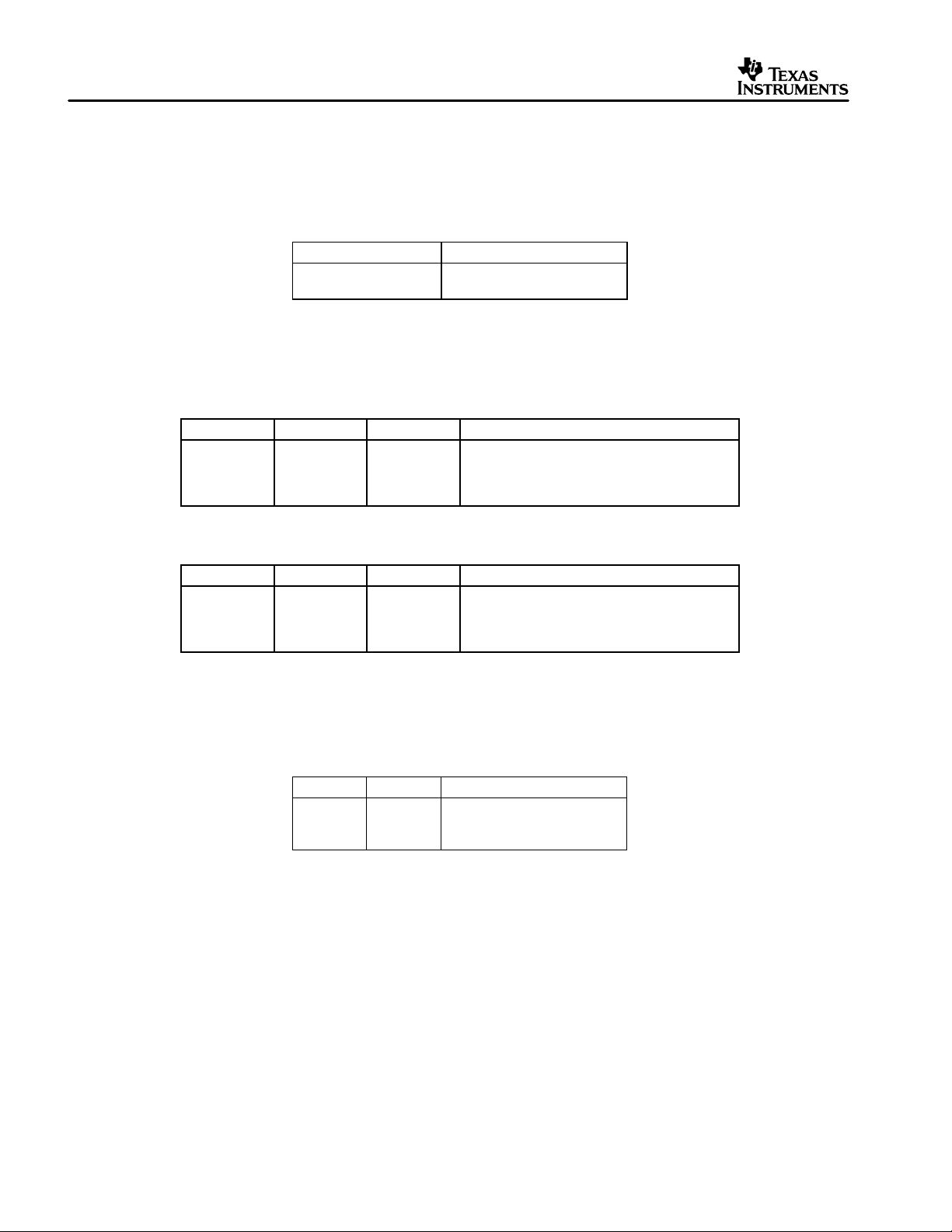
The operation of de-emphasis on the PCM3008 is controlled by SW1 and SW2.
SW1 (DEM0) SW2 (DEM1) De-emphasis
L
H
L
H
The operation of the power-down mode for the DAC is controlled by SW3, and for the ADC by SW4.
SW3 (PDDA) DAC Operation
L
H
L
L
H
H
Power-down mode
Normal operation
SLEU006
44.1 kHz
OFF
48 kHz
32 kHz
SW4 (PDAD) ADC Operation
L
H
Power-down mode
Normal operation
DEM-DAI3008 PCM3008 Evaluation Board
3
Page 4
SLEU006
3.1.2 Power Supply Connections
The PCM3008 daughterboard can accept power from either of two sources. Either 2.4 V supplied via
CN-1 powers the board directly, or an onboard 2.5-V regulator powers the PCM3008 using a 5-V source.
The 5-V power comes from the 5-V supply on the DAI motherboard via connector CN-2. Power source
selection is accomplished by the use of jumper JP1.
JP-1 Setting Power Supply Selected
1-2
3-4
3.2 DAI Motherboard Controls
3.2.1 Switch Settings
Selection of the audio output interface format for the DAI receiver is controlled by SW3, SW2, and SW1.
SW3(M2) SW2(M1) SW1(M0) Audio Format
L
L
H
H
NOTE: JP6 must be connected INV when 16–24-bit, left-justified is selected.
L
H
L
H
5 V at CN-2
2.4 V at CN-1
L
L
H
L
16–24-bit, MSB-first, left-justified
IIS
16-bit, MSB-first, right-justified
18-bit, MSB-first, right-justified
Selection of the audio input interface format for the DAI transmitter is controlled by SW4, SW5, and SW6.
SW4(M2) SW5(M1) SW6(M0) Audio Format
L
H
H
H
L
L
L
H
H
L
H
L
16–24-bit, MSB-first, left-justified
IIS
16-bit, MSB-first, right-justified
18-bit, MSB-first, right-justified
The operating mode and sampling frequency of the DAI transmitter are selected using PRO, FC1, and
FC0 on SW9.
PRO: H = Consumer mode, L = Professional mode
FC1: Channel status bit 24 in consumer mode
FC0: Channel status bit 25 in consumer mode
FC1 FC0 Sampling Frequency
L
L
H
L
H
L
44.1 kHz
48 kHz
32 kHz
The remaining switches on SW9 are labelled C2, C3, C8, C9, and C15. They are used for the selection of
channel status bits from the CS8404, and correspond to channel status bits 2, 3, 8, 9, and 15,
respectively.
SW7 is the master/slave selection switch. It must be set to slave for proper operation the DAC and codec
of the PCM3008.
3.2.2 Jumper Selections
JP1 selects the system clock source.
XTAL: Sysem clock generated by onboard XTAL oscillator module
NML: System clock generated by DAI receiver
INV: Inverted system clock generated by DAI receiver
4
DEM-DAI3008 PCM3008 Evaluation Board
Page 5
JP2 selects the BCK clock source.
DIR: BCK clock generated by DAI receiver
256/384/512: BCK clock generated by XTAL oscillator
SLEU006
JP3 selects the LRCK (f
) clock source.
s
DIR: LRCK clock generated by DAI receiver
256/384/512: LRCK clock generated by XTAL oscillator
JP4 selects the clock frequency of the XTAL oscillator clock.
256/512fs: for 256 f
384fs: for 384 f
or 512 fs operation
s
operation
s
JP5 selects the DAI transmitter clock source.
512,384 : 384 f
DIR1: 256 f
or 512 fs XTAL clock
s
clock from XTAL clock or clock generated by DAI receiver
s
DIR2: Transparent operating mode for DAI transmitter
NOTE: In certain applications it is desirable to receive digital audio data with the CS8412 and retransmit
it with the CS8402. In these situations, user and validity information and channel status must pass through
unaltered. Details of transparent operation are described in Crystal’s CS8402 data sheet.
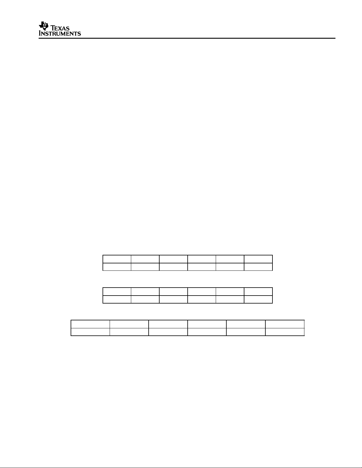
3.2.3 Typical Board Settings
Jumper settings that are considered appropriate for some typical operating conditions are listed in the
following tables.
Typical settings for DAC operation
JP1 JP2 JP3 JP4 JP5 JP6
NML DIR DIR – – NML
Typical settings for ADC operation by DAI receiver clock
JP1 JP2 JP3 JP4 JP5 JP6
NML DIR DIR – DIR1 NML
Typical settings for ADC operation by XTAL clock
JP1 JP2 JP3 JP4 JP5 JP6
XTAL 256 to 512 256 to 512 256 to 512 512/DIR1 NML
4 Physical and Electrical
The silkscreen of the PCM3008 daughterboard is shown in Figure 3, and the top and bottom copper layers
are shown in Figure 4 and Figure 5, respectively. Figure 6 is the schematic of the daughterboard, and the
schematic of the motherboard is in Appendix A.
DEM-DAI3008 PCM3008 Evaluation Board
5
Page 6

SLEU006
Figure 3. DEM-DAI3008 Board Silkscreen
6
DEM-DAI3008 PCM3008 Evaluation Board
Page 7

SLEU006
Figure 4. DEM-DAI3008 Board Top Copper Layer
DEM-DAI3008 PCM3008 Evaluation Board
7
Page 8

SLEU006
Figure 5. DEM-DAI3008 Board Bottom Copper Layer
8
DEM-DAI3008 PCM3008 Evaluation Board
Page 9

SLEU006
SCKI
GND
LRCK
DIN
BCK
DOUT
CN-5
UD1
74LCX244F
C11
10 µF
C12
0.1 µF
GND +2.4V V
C1
100 µF
C2
0.1 µF
+
JP-2
R1
10 Ω
P
CC
CN-1
JP-1
1
+
0.1 µF
A
B
C5
C6
10 µF
10 µF
C4
2
UP1
78L2.5
43
U1
PCM3008
V
OUT
COM
+
V
OUT
PDDAVINL 143
PDADGND 134
+
CC
SYSCKDEM0 116
LRCKDEM1 107
BCKV
DINDOUT
+
161
RV
LVINR
152
125
98
GND +5V V
C3
1 µF
10 µF
+
+
C
10 µF
D
C7
C8
CC
CN-2
CN-3
V
OUT
V
OUT
GND
L
R
+
C9
1 µF
P
SW-1 – SW-4
A B C D
VINLVINRGND
+
C10
1 µF
CN-4
Figure 6. DEM-DAI3008 Schematic Diagram
DEM-DAI3008 PCM3008 Evaluation Board
9
Page 10

SLEU006
Appendix A DEM-DAI Motherboard Schematic Diagram
10
DEM-DAI3008 PCM3008 Evaluation Board
Page 11

Page 12

EVM IMPORTANT NOTICE
Texas Instruments (TI) provides the enclosed product(s) under the following conditions:
This evaluation kit being sold by TI is intended for use for ENGINEERING DEVELOPMENT OR EV ALUA TION
PURPOSES ONL Y and is not considered by TI to be fit for commercial use. As such, the goods being provided
may not be complete in terms of required design-, marketing-, and/or manufacturing-related protective
considerations, including product safety measures typically found in the end product incorporating the goods.
As a prototype, this product does not fall within the scope of the European Union directive on electromagnetic
compatibility and therefore may not meet the technical requirements of the directive.
Should this evaluation kit not meet the specifications indicated in the EVM User’s Guide, the kit may be returned
within 30 days from the date of delivery for a full refund. THE FOREGOING WARRANTY IS THE EXCLUSIVE
WARRANTY MADE BY SELLER TO BUYER AND IS IN LIEU OF ALL OTHER WARRANTIES, EXPRESSED,
IMPLIED, OR ST ATUT ORY, INCLUDING ANY WARRANTY OF MERCHANT ABILITY OR FITNESS FOR ANY
PARTICULAR PURPOSE.
The user assumes all responsibility and liability for proper and safe handling of the goods. Further, the user
indemnifies TI from all claims arising from the handling or use of the goods. Please be aware that the products
received may not be regulatory compliant or agency certified (FCC, UL, CE, etc.). Due to the open construction
of the product, it is the user’s responsibility to take any and all appropriate precautions with regard to electrostatic
discharge.
EXCEPT TO THE EXTENT OF THE INDEMNITY SET FORTH ABOVE, NEITHER P ARTY SHALL BE LIABLE
TO THE OTHER FOR ANY INDIRECT, SPECIAL, INCIDENTAL, OR CONSEQUENTIAL DAMAGES.
TI currently deals with a variety of customers for products, and therefore our arrangement with the user is not
exclusive.
TI assumes no liability for applications assistance, customer product design, software performance, or
infringement of patents or services described herein.
Please read the EVM User’s Guide and, specifically, the EVM Warnings and Restrictions notice in the EVM
User’s Guide prior to handling the product. This notice contains important safety information about temperatures
and voltages. For further safety concerns, please contact the TI application engineer.
Persons handling the product must have electronics training and observe good laboratory practice standards.
No license is granted under any patent right or other intellectual property right of TI covering or relating to any
machine, process, or combination in which such TI products or services might be or are used.
Mailing Address:
Texas Instruments
Post Office Box 655303
Dallas, Texas 75265
Copyright 2001, Texas Instruments Incorporated
Page 13

EVM WARNINGS AND RESTRICTIONS
It is important to operate this EVM within the input voltage range of V
+ 0.3 V (V
CC
CC
= 2.8
to 3.6 V) and the output voltage range of "5 Vdc and 2 V ac.
Exceeding the specified input range may cause unexpected operation and/or irreversible
damage to the EVM. If there are questions concerning the input range, please contact a TI
field representative prior to connecting the input power.
Applying loads outside of the specified output range may result in unintended operation and/or
possible permanent damage to the EVM. Please consult the EVM User’s Guide prior to
connecting any load to the EVM output. If there is uncertainty as to the load specification,
please contact a TI field representative.
During normal operation, some circuit components may have case temperatures greater than
60°C. The EVM is designed to operate properly with certain components above 60°C as long
as the input and output ranges are maintained. These components include but are not limited
to linear regulators, switching transistors, pass transistors, and current sense resistors. These
types of devices can be identified using the EVM schematic located in the EVM User’s Guide.
When placing measurement probes near these devices during operation, please be aware
that these devices may be very warm to the touch.
Mailing Address:
Texas Instruments
Post Office Box 655303
Dallas, Texas 75265
Copyright 2001, Texas Instruments Incorporated
Page 14

IMPORTANT NOTICE
T exas Instruments and its subsidiaries (TI) reserve the right to make changes to their products or to discontinue
any product or service without notice, and advise customers to obtain the latest version of relevant information
to verify, before placing orders, that information being relied on is current and complete. All products are sold
subject to the terms and conditions of sale supplied at the time of order acknowledgment, including those
pertaining to warranty, patent infringement, and limitation of liability.
TI warrants performance of its products to the specifications applicable at the time of sale in accordance with
TI’s standard warranty . T esting and other quality control techniques are utilized to the extent TI deems necessary
to support this warranty . Specific testing of all parameters of each device is not necessarily performed, except
those mandated by government requirements.
Customers are responsible for their applications using TI components.
In order to minimize risks associated with the customer’s applications, adequate design and operating
safeguards must be provided by the customer to minimize inherent or procedural hazards.
TI assumes no liability for applications assistance or customer product design. TI does not warrant or represent
that any license, either express or implied, is granted under any patent right, copyright, mask work right, or other
intellectual property right of TI covering or relating to any combination, machine, or process in which such
products or services might be or are used. TI’s publication of information regarding any third party’s products
or services does not constitute TI’s approval, license, warranty or endorsement thereof.
Reproduction of information in TI data books or data sheets is permissible only if reproduction is without
alteration and is accompanied by all associated warranties, conditions, limitations and notices. Representation
or reproduction of this information with alteration voids all warranties provided for an associated TI product or
service, is an unfair and deceptive business practice, and TI is not responsible nor liable for any such use.
Resale of TI’s products or services with
that product or service voids all express and any implied warranties for the associated TI product or service,
is an unfair and deceptive business practice, and TI is not responsible nor liable for any such use.
Also see: Standard T erms and Conditions of Sale for Semiconductor Products.
Copyright 2001, Texas Instruments Incorporated
statements different from or beyond the parameters
www.ti.com/sc/docs/stdterms.htm
Mailing Address:
Texas Instruments
Post Office Box 655303
Dallas, Texas 75265
stated by TI for
 Loading...