

Page 1
查询DEM-ADS1216供应商
www.ti.com
DEM-ADS1216
EVALUATION FIXTURE
FEATURES
● PROVIDES FAST AND EASY
PERFORMANCE TESTING FOR ADS1216
● SEPARATE ANALOG AND DIGITAL
POWER
● PC PRINTER PORT CONTROL
● WINDOWS® 95/98 SOFTWARE
Windows is a registered trademark of Microsoft Corp.
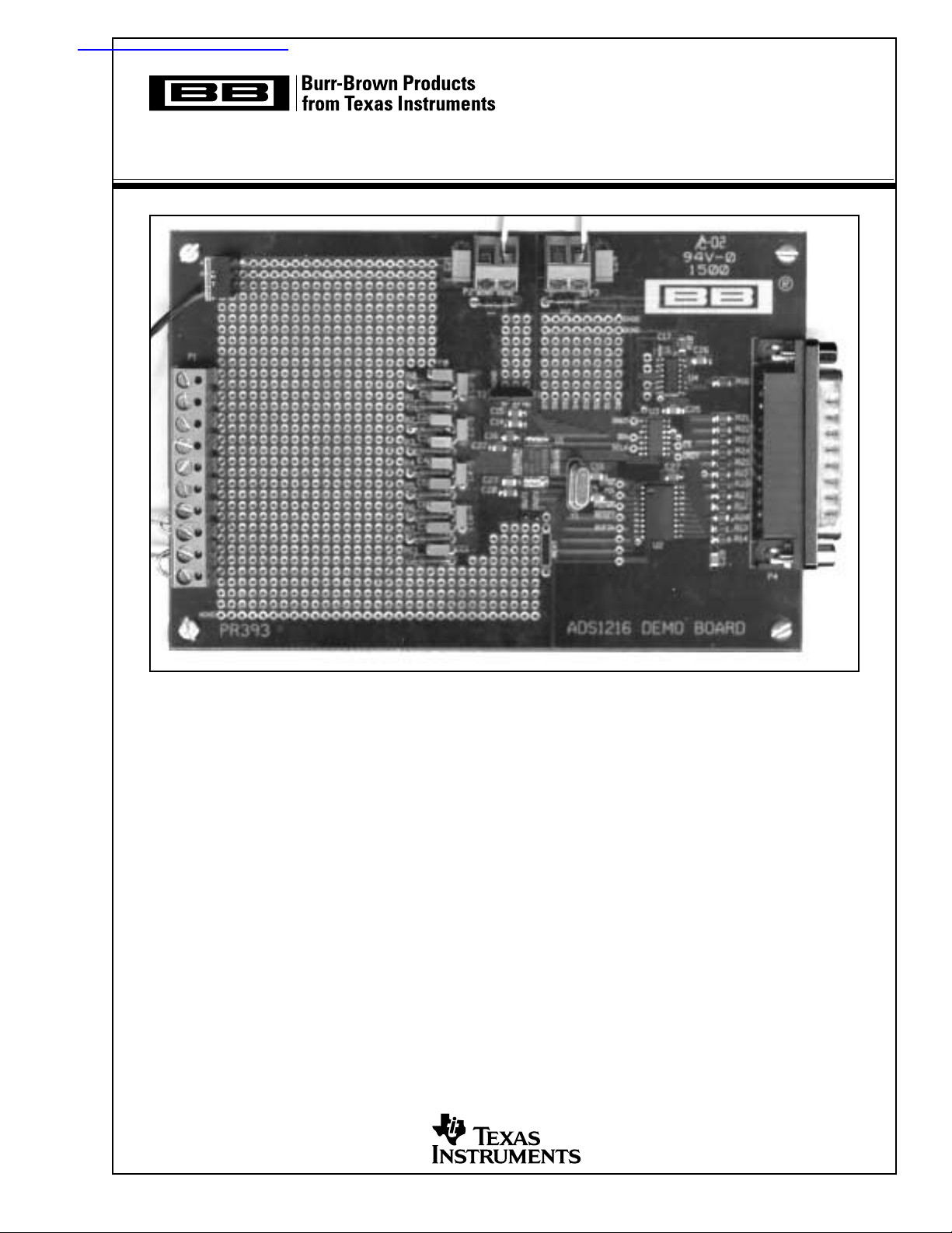
DESCRIPTION
The DEM-ADS1216 demo board is designed for ease
of use when evaluating the ADS1216 high resolution
analog-to-digital converter. The ADS1216 offers
24-bits no missing codes performance. It has 8 input
channels that can be configured as up to 8 differential
channels. The multiplexer is followed by a programmable gain amplifier with selectable gains of up to
128.
Hardware options include user defined clock frequency,
internal or external reference, and input biasing.
All of the features and functionality of the ADS1216
can be exercised using the pull-down menus available
from the DEM-ADS1216 software.
Copyright © 2001, Texas Instruments Incorporated SBAU038 Printed in U.S.A. February, 2001
Page 2
INITIAL CONFIGURATION
WINDOWS SOFTWARE
The DEM-ADS1216 is designed to be operational without any
user configuration except connecting the power supplies and the
communications cable to the PC printer port. To use the internal
reference voltage, jumpers T1 and T2 should be installed.
POWER SUPPLY
The analog and digital supplies should be connected together at the power supply. That means that a pair of wires
should go from VCC and AGND to the power supply and a
separate pair of wires should go from VDD and DGND to the
same +5Vpower supply.
VOLTAGE REFERENCE
With jumpers T1 and T2 installed the DEM-ADS1216 Demo
Board will use the internal reference. These jumpers can be
replaced and connections made to the pins, to use an external
reference.
CLOCK
A 2.4576MHz crystal is connected to the XIN and XOUT
pins to provide a convienient frequency for 60Hz rejection.
PC BOARD LAYOUT
The DEM-ADS1216 demo board consists of a 2-layer PC
board. To achieve the highest level of performance, surfacemount components are used wherever possible. This reduces
the trace length and minimizes the effects of parasitic capacitance and inductance. The demo board has a divided ground
with all the analog signals over one portion and the digital
signals in the other. Keep in mind that this approach may not
necessarily yield optimum performance results when designing the ADS1216 into different individual applications. In any
case, thoroughly bypassing the power supply and reference
pins of the converter is strongly recommended.
The breadboard area is provided so that input filters can be
added. As shipped, the board includes an R-C filter (49.9Ω
and 47pF) on each input with 0.1µF differential capacitor
between adjacent channels.
The ADS1216 uses registers and a 1-byte opcode to control
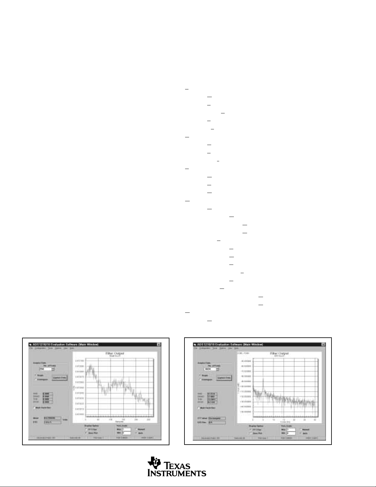
the operation. The evaluation software provides a convenient method to issue the commands and receive the results.
It also can display the results of acquired data, as shown in
Figure 1, and perform a frequency analysis, as shown in
Figure 2.
The program is organized with pull-down menus as follows:
File
Display Data List
Save Data
Save FFT Data
Print Data
Exit
Configuration
Configure Digital Filter
Select Input Channel
Set IDACs/PGA/V
Tests
Opcode Test
RAM R/W Test
Noise Test
Options
Data List Format
Voltage
Raw Hex
Raw Decimal
Set FFT Window
Rectangular
Hamming
Blackman
Blackman Harris
Continuous 5th Derivative
FFT Harmonic Bins
Number of Harmonic Bins
Number of DC Bins
Help
About ADS1216 Demo SW
REF
FIGURE 1. Time Plot. FIGURE 2. FFT Frequency Plot.
2
DEM-ADS1216
SBAU038
Page 3
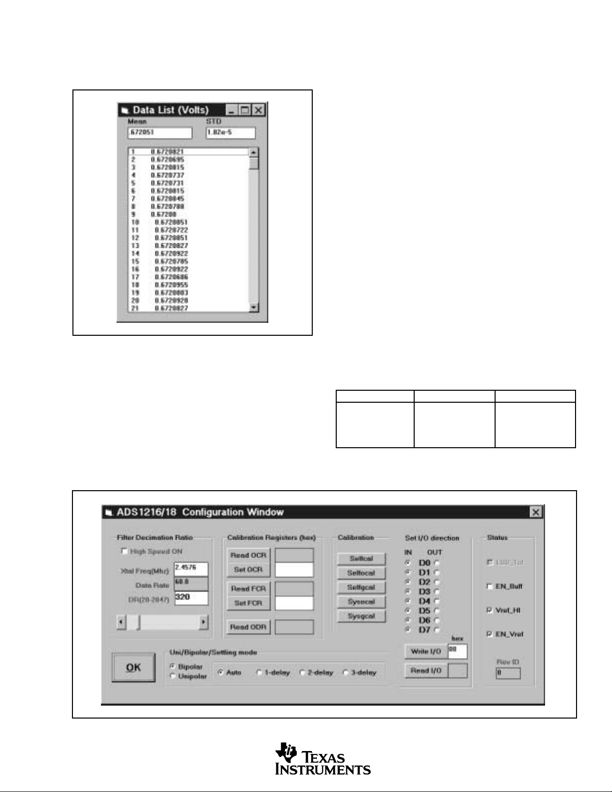
SAVE DATA
The Save Data List shown in Figure 3 displays the individual
data values as well as the mean and standard decimation of
the data.
FIGURE 3. Data List.
CONFIGURATION
The Configure Digital Filter opens a window that provides
many options, as shown in Figure 4.
Filter Decimation Ratio
The Filter Decimation Ratio box allows you to adjust the
decimation ratio with the scroll bar or by entering the value
in the box at the bottom. Additionally, as you change the
decimation ratio, you can observe the resulting data rate.
Calibration Registers
The current values of the Offset, Full-Scale Output Data
registers can be read and displayed. Additionally, these
values can be changed by entering a new HEX value in the
field and pushing the set button.
Calibration
Five types of calibration can be performed. When the button
is pushed the ADS1216 performs the calibration then it
reads back and displays the results in the calibration registers. The five types of calibration are:
1) Selfcal—Both Offset and Gain Calibration
2) Selfocal—Only Offset Calibration
3) Selfgcal—Only Gain Calibration
4) Sysocal—Offset Calibration, Input = 0V
5) Sysgcal—Gain Calibration, Input = V
REF
Set I/O Direction
The eight pins of I/O can be individually set for output or
input. The output pins will be set to the HEX value entered
in the “Write I/O” field when the “Write I/O” button is
selected. The value of all pins will be displayed in the box
next to the “Read I/O” button when it is selected.
Status
The various control bits can be set and monitored in the
status box. Additionally, the revision ID of the ADS1216
will be displayed. The status bits and their functions are
shown in Table I.
01
st
LSB_1
EN_Buff No Input Buffer Input Buffer Enabled
V
_HI V
REF
EN_V
REF
Send MSB First Send LSB First
= 1.25V V
REF
V
OFF V
REF
REF
REF
= 2.5V
ON
TABLE I. Control Bits.
FIGURE 4. Configuration Window.
DEM-ADS1216
SBAU038
3
Page 4

Unipolar/Bipolar
The results of the unipolar/bipolar selection are shown in
Table II.
ANALOG INPUT DIGITAL OUTPUT
Bipolar Zero 0x000000
Unipolar Zero 0x000000
+FSR 0x7FFFFF
-FSR 0x800000
+FSR 0xFFFFFF
-FSR 0x000000
TABLE II. Unipolar/Bipolar Selection Results.
Settling Mode
Three Sinc filters can be selected. When the input changes,
the fast settling filter settles in one data output interval, Sinc
settles in two periods, and Sinc3 takes three periods to fully
settle. However, the Sinc3 filter has the highest resolution.
The desired filter can be selected. Auto mode selects the fast
settling filter when the input changes, then it changes to the
Sinc2 filter for the second period, and on the third data out
period it will use the output of the Sinc
3
filter. This gives fast
settling when the input channel changes, but the same highresolution results after the necessary number of conversion
periods.
OK
Selecting OK will save the selected setup.
Calibrate Internal Temp Sensor
The Calibrate Temp button opens the Internal Temp Sensor
Calibration window for calibration of the internal temperature diode. This allows you to force the temperature readout
to match the temperature you enter. This is not intented to
give a high-accuracy temperature readout, but will give a
reading that is reasonable for a single diode voltage measurement.
2
FIGURE 6. Temperature Calibration.
SET IDAC
/PGA/V
S
REF
The screen shown in Figure 7 provides the means to observe
the interaction of the IDAC settings, R
EXT
and V
tionally, the PGA can be set from this screen.
REF
. Addi-
SELECT INPUT CHANNELS
Figure 5 gives a graphical method to select the multiplexer
channel. This also shows the full flexibility of the ADS1216
multiplexer, which allows any input to be selected as the
positive or negative input for a measurement. The mouse
selects which switch to close. Additionally, the internal
diode can be connected, which turns on the burn out current
sources. By measuring the voltage on the diode, a temperature measurement can be made. IDAC1 can also drive this
sensing diode.
FIGURE 7. PGA Settings.
FIGURE 5. Input Multiplexer.
4
DEM-ADS1216
SBAU038
Page 5

TEST SCREENS
Opcode Test.
The screen in Figure 8 allows the opcodes to be tested and
the results observed.
FIGURE 8. Opcode Control.
One convenient way to test the communications and operations of the ADS1216 Demo software is to go to this screen,
select “Reset”, and then “Read all Regs”. You should end up
with a register dump that looks like Figure 9.
FIGURE 10. Ram Test.
FIGURE 9. Reset Condition.
You can observe that the reset state of the registers are: F6,
10, 00, 00, 00, 00, 00, FF, F0, 00, 00, 00, 00, 22, 90, 67.
This screen also shows the state of the digital control signals.
Any opcode can be entered and tested to observe the results
RAM R/W Test
The test screen in Figure 10 provides tools for testing RAM.
Various simple operations have been assigned to a button.
Additionally, a full RAM test can be executed with the “Test
Ram” button. This clears RAM, generates random data,
writes to the RAM and verifies that the contents matches the
random data.
Noise Test
This test provides an automated means to verify the performance of the ADS1216 across various decimation ratio
values, PGA settings and with averaging of the results. With
all the options selected, this test can take a long time to
complete. The results are displayed in a tabular format,
which shows the PGA settings, Decimation Rate, Average
Output, Standard Decmiation, and Effective number of bits,
as shown in Figure 11.
FIGURE 11. Noise Test Results.
DEM-ADS1216
SBAU038
The “File” menu selection gives you the option to save your
data. All data is saved in a comma delimited format so that
it can be imported into a spreadsheet for further analysis.
5
Page 6

FIGURE 12. Schematic.
6
DEM-ADS1216
SBAU038
Page 7

TOP (TRACES AND GND PLANE)
FIGURE 13. Top Layer.
BOTTOM (TRACES AND GND PLANE)
FIGURE 14. Bottom Layer.
DEM-ADS1216
SBAU038
7
Page 8

COMPONENT LIST
PART NUMBER DESCRIPTION REF. DES. QTY VENDOR PART NUMBER MANUFACTURER
ADS1216 20-BIT A/D Converter U1 1 ADS1216 Burr-Brown
CK05BX104K CAP, 0.10µF, 50V, 10%, CERAMIC X7R C0-1,C2-3,C4-5,C6-7 4 CK05BX104K KEMET
CK05BX470K CAP, 47pF, 200V, 10%, CERAMIC X7R C0,C1,C2,C3,C4,C5 9 CK05BX470K KEMET
* C6,C7,CC1
CRCW12061001F RES, 1.0KΩ, 0.125W, 1%, CHIP-THICK-FILM R10 1 CRCW12061001F DALE
CRCW12062000F RES, 200Ω, 0.125W, 1%, CHIP-THICK-FILM R12,R13,R14,R15,R16 13 CRCW12062000F DALE
* R21,R22,R23,R24,R25
* R26,R27,R28
C1206C100K1GAC CAP, 10pF, 100V, 10%, CHIP-CERAMIC COG C28 1 C1206C100K1GAC KEMET
C1206C104K5RAC CAP, 0.10µF, 50V, 10%, CHIP-CERAMIC X7R C14,C15,C16,C20,C22 9 C1206C104K5RAC KEMET
C23,C25,C26,C27
C1206C220K1GAC CAP, 22pF, 100V, 10%, CHIP-CERAMIC COG C18,C19 2 C1206C220K1GAC KEMET
ED 120/10 OST 10-Pin TERM BLK;0.2 OC P1 1 ED 120/10
ED 300/2 2 PIN TERMINAL BLK; 5MM PITCH P2,P3 2 ED 300/2
HC49 2.4576MHz CRYSTAL;CTS;Cell HC18U Y1 1 HC49
P6KE6.8A ZENER 6.8V D1,D2 2 P6KE6.8A
REG1117-5 +5V Regulator Q1 1 REG1117-5 Burr-Brown
RN55C49R9F RES, 49.9Ω, 0.125W, 1%, METAL-FILM R0,R1,R2,R3,R4,R5 9 RN55C49R9F DALE
* R6,R7,RC1
RN55C1000F RES, 100Ω 0.125W, 1%, METAL-FILM R11 1 RN55C1000F DALE
TSW-1-S01-06-S 1-Pin TERMINAL; CELL TP042 T3,T4,T5,T6,T7,T8 28 TSW-1-S01-06-S
* T9,T10,T15,T16,T17
* T18,T19,T20,T21,T22
* T24,T25,T26,T27,T28
* T29,T30,T31,T32,T33
* T34,T35
TSW-102-07-L-S CONN, 2 POS .1 CTR .025 SQ. POST T1,T2,T36,T37 4 TSW-102-07-L-S
T491B105K350AS
T491D106K035AS
74hct04d IC, Inverter, hex U3 1 74hct04d
74hct74d IC, Flip Flop, Dual J-K with clear & preset U4 1 74hct74d
74hct245dw IC, Bus Transceiver, Octal, 3-state outputs U2 1 74hct245dw
747842-6 25 Pin Right Angle Male D Conn P4 1 747842-6
CAP, 1µF, 35V, 10%, TANTALUM CHIP-MOLDED
CAP, 10µF, 35V, 10%, TANTALUM CHIP-MOLDED
C17 1 T491B105K035AS KEMET
C21,C24 2 T491D106K035AS KEMET
8
DEM-ADS1216
SBAU038
Page 9

IMPORTANT NOTICE
T exas Instruments and its subsidiaries (TI) reserve the right to make changes to their products or to discontinue
any product or service without notice, and advise customers to obtain the latest version of relevant information
to verify, before placing orders, that information being relied on is current and complete. All products are sold
subject to the terms and conditions of sale supplied at the time of order acknowledgment, including those
pertaining to warranty, patent infringement, and limitation of liability.
TI warrants performance of its products to the specifications applicable at the time of sale in accordance with
TI’s standard warranty . T esting and other quality control techniques are utilized to the extent TI deems necessary
to support this warranty . Specific testing of all parameters of each device is not necessarily performed, except
those mandated by government requirements.
Customers are responsible for their applications using TI components.
In order to minimize risks associated with the customer’s applications, adequate design and operating
safeguards must be provided by the customer to minimize inherent or procedural hazards.
TI assumes no liability for applications assistance or customer product design. TI does not warrant or represent
that any license, either express or implied, is granted under any patent right, copyright, mask work right, or other
intellectual property right of TI covering or relating to any combination, machine, or process in which such
products or services might be or are used. TI’s publication of information regarding any third party’s products
or services does not constitute TI’s approval, license, warranty or endorsement thereof.
Reproduction of information in TI data books or data sheets is permissible only if reproduction is without
alteration and is accompanied by all associated warranties, conditions, limitations and notices. Representation
or reproduction of this information with alteration voids all warranties provided for an associated TI product or
service, is an unfair and deceptive business practice, and TI is not responsible nor liable for any such use.
Resale of TI’s products or services with
that product or service voids all express and any implied warranties for the associated TI product or service,
is an unfair and deceptive business practice, and TI is not responsible nor liable for any such use.
Also see: Standard T erms and Conditions of Sale for Semiconductor Products.
Copyright 2001, Texas Instruments Incorporated
statements different from or beyond the parameters
www.ti.com/sc/docs/stdterms.htm
Mailing Address:
Texas Instruments
Post Office Box 655303
Dallas, Texas 75265
stated by TI for
 Loading...