

Page 1
Please be aware that an important notice concerning availability, standard warranty, and use in critical applications of Texas Instruments
查询DDC118供应商
DDC118
SBAS325A − JUNE 2004 − REVISED JUNE 2005
Octal Current Input 20-Bit
Analog-To-Digital Converter
FEATURES
D SINGLE-CHIP SOLUTION TO DIRECTLY
MEASURE EIGHT LOW-LEVEL CURRENTS
D HIGH PRECISION, TRUE INTEGRATING
FUNCTION
D INTEGRAL LINEARITY:
±0.01% of Reading ±0.5ppm of FSR
D VERY LOW NOISE: 5.2ppm of FSR
D LOW POWE R: 13.5mW/channel
D ADJUSTABLE DATA RATE: Up to 3.125kSPS
D PROGRAMMABLE FULL SCALE
D DAISY-CHAINABLE SERIAL INTERFACE
VREF DVDDAVDD
CLK
Control
Digital
CONV
RANGE0
RANGE1
RANGE2
TEST
CLK_4X
HISPD/LOPWR
RESET
FORMAT
DCLK
DCLK
DVALID
DOUT
DOUT
DIN
DIN
IN1
IN3
IN2
IN4
IN5
IN7
IN6
IN8
Dual
Switched
Integrator
Dual
Switched
Integrato r
Dual
Switched
Integrator
Dual
Switched
Integrator
Dual
Switched
Integrator
Dual
Switched
Integrato r
Dual
Switched
Integrator
Dual
Switched
Integrator
∆Σ
Modulator
∆Σ
Modulator
∆Σ
Modulator
∆Σ
Modulator
Digital
Filter
Digital
Filter
Digital
Filter
Digital
Filter
Input/Output
DGNDAGND
APPLICATIONS
D CT SCANNER DAS
D PHOTODIODE SENSORS
D INFRARED PYROMETER
D LIQUID/GAS CHROMATOGRAPHY
Protected b y U S Patent #5841310
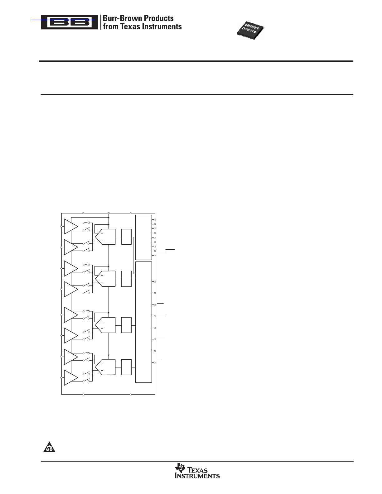
DESCRIPTION
The DDC118 is a 20-bit octal channel, current-input
analog-to-digital (A/D) converter. It combines both
current-to-voltage and A/D conversion so that eight
low-level current output devices, such as photodiodes, can
be directly connected to its inputs and digitized.
For each of the eight inputs, the DDC118 provides a
dual-switched integrator front-end. This design allows for
continuous current integration: while one integrator is
being digitized by the onboard A/D converter, the other is
integrating the input current. Adjustable full-scale ranges
from 12pC to 350pC and adjustable integration times from
50µs to 1s allow currents from fAs to µAs to be measured
with outstanding precision. Low-level linearity is ±0.5ppm
of the full-scale range and noise is 5.2ppm of the full-scale
range.
Two modes of operation are provided. In Low-Power
mode, total power dissipation is only 13.5mW per channel
with a maximum data rate of 2.5kSPS. High-Speed mode
supports data rates up to 3.125kSPS with a corresponding
dissipation of 18mW per channel.
The DDC118 has a serial interface designed for
daisy-chaining in multi-device systems. Simply connect
the output of one device to the input of the next to create
the chain. Common clocking feeds all the devices in the
chain so that the digital overhead in a multi-DDC118
system is minimal.
The DDC118 is a single-supply device using a +5V analog
supply and supporting a +2.7V to +5.25V digital supply.
Operating over the industrial temperature range of −40°C
to 85°C, the DDC118 is offered in a QFN-48 package.
semiconductor products and disclaimers thereto appears at the end of this data sheet.
All trademarks are the property of their respective owners.
! !
www.ti.com
Copyright 2002−2005, Texas Instruments Incorporated
Page 2

""#
SBAS325A − JUNE 2004 − REVISED JUNE 2005
www.ti.com
ABSOLUTE MAXIMUM RATINGS
Analog Input Current 750µA. . . . . . . . . . . . . . . . . . . . . . . . . . . . . . .
AVDD to DVDD −0.3V to +6V. . . . . . . . . . . . . . . . . . . . . . . . . . . . . . .
AVDD to AGND −0.3V to +6V. . . . . . . . . . . . . . . . . . . . . . . . . . . . . .
DVDD to DGND −0.3V to +6V. . . . . . . . . . . . . . . . . . . . . . . . . . . . . .
AGND to DGND ±0.2V. . . . . . . . . . . . . . . . . . . . . . . . . . . . . . . . . . .
VREF Input to AGND 2.0V to AVDD + 0.3V. . . . . . . . . . . . . . . . . .
Analog Input to AGND −0.3V to +0.7V. . . . . . . . . . . . . . . . . . . . . . .
Digital Input Voltage to DGND −0.3V to DVDD + 0.3V. . . . . . . . . . .
Digital Output Voltage to DGND −0.3V to AVDD + 0.3V. . . . . . . . .
Operating Temperature −40°C to +85°C. . . . . . . . . . . . . . . . . . . . . .
Storage Temperature −60°C to +150°C. . . . . . . . . . . . . . . . . . . . . . .
Junction Temperature (TJ) +150°C. . . . . . . . . . . . . . . . . . . . . . . . . . .
(1)
Stresses above these ratings may cause permanent damage.
Exposure to absolute maximum conditions for extended periods
may degrade device reliability. These are stress ratings only , an d
functional operation of the device at these or any other conditions
beyond those specified is not implied.
(1)
This integrated circuit can be damaged by ESD. Texas
Instruments recommends that all integrated circuits be
handled with appropriate precautions. Failure to observe
proper handling and installation procedures can cause damage.
ESD damage can range from subtle performance degradation to
complete device failure. Precision integrated circuits may be more
susceptible t o damage because very small parametric changes could
cause the device not to meet its published specifications.
ORDERING INFORMATION
For package and ordering information, see the Package
Option Addendum located at the end of this data sheet.
2
Page 3
""#
Integration Time, T
Integral Linearity Error
(6)
Resolution
www.ti.com
SBAS325A − JUNE 2004 − REVISED JUNE 2005
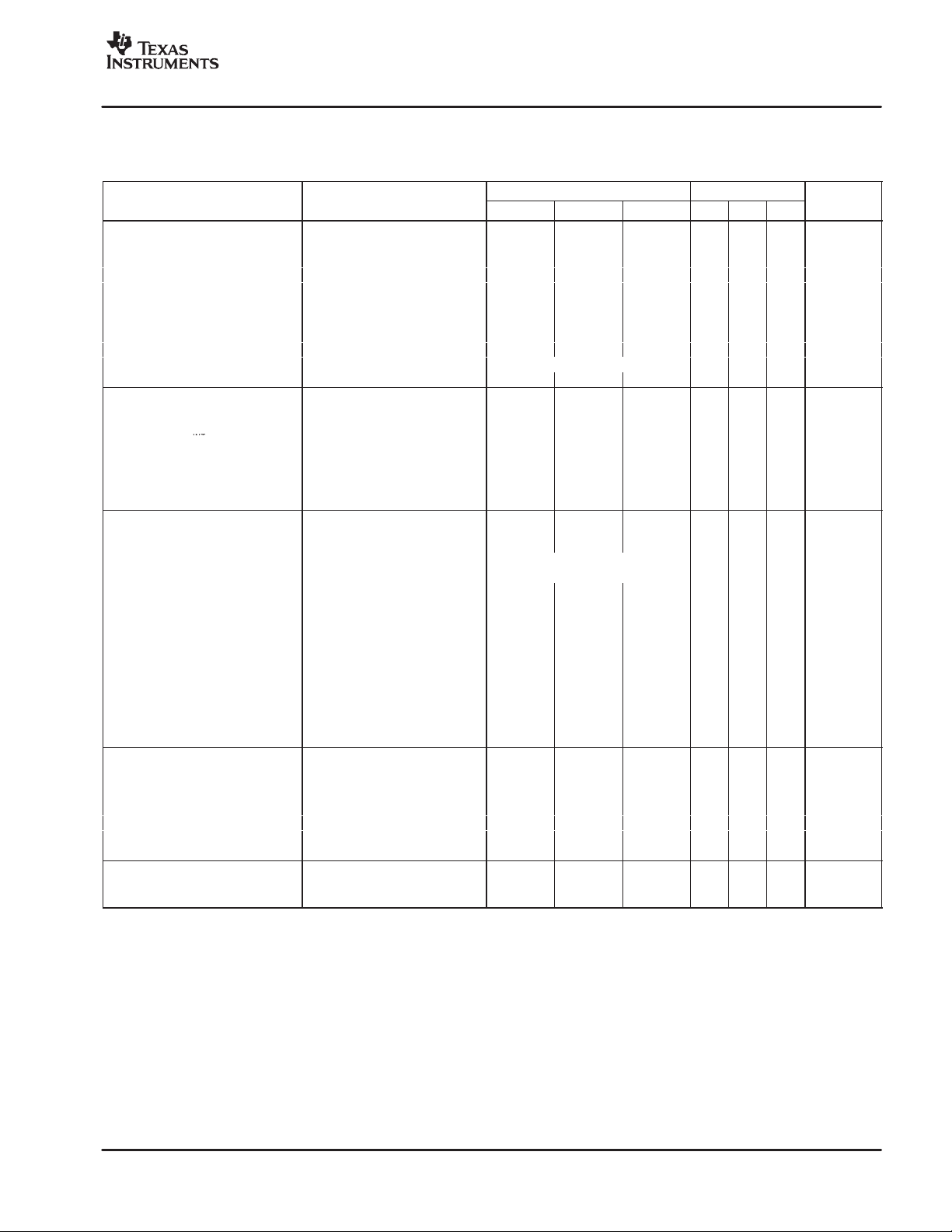
ELECTRICAL CHARACTERISTICS
At TA = +25°C, AVDD = +5V, DVDD = 3V, VREF = +4.096V, Range 5 (250pC), and continuous mode operation, unless otherwise noted.
Low-Power Mode: T
PARAMETER TEST CONDITIONS MIN TYP MAX MIN TYP MAX UNITS
ANALOG INPUT RANGE
Range 0 10.2 12 13.8 ∗
Range 1 47.5 50 52.5 ∗ ∗ ∗ pC
Range 2 95 100 105 ∗ ∗ ∗ pC
Range 3 142.5 150 157.5 ∗ ∗ ∗ pC
Range 4 190 200 210 ∗ ∗ ∗ pC
Range 5 237.5 250 262.5 ∗ ∗ ∗ pC
Range 6 285 300 315 ∗ ∗ ∗ pC
Range 7 332.5 350 367.5 ∗ ∗ ∗ pC
Negative Full-Scale Range −0.4% of Positive Full-Scale Range ∗ pC
Input Current
DYNAMIC CHARACTERISTICS
Data Rate 2.5 3.125 kSPS
System Clock Input (CLK)
Data Clock (DCLK) 16 ∗ MHz
ACCURACY
Noise, Low-Level Input
Resolution FORMAT = 1 20 ∗ Bits
Input Bias Current 0.1 10 ∗ ∗ pA
Range Error Match
Range Sensitivity to VREF V
Offset Error Range 5 (250pC) ±400 ±1000 ∗ ∗ ppm of FSR
Offset Error Match
DC Bias Voltage
Power-Supply Rejection Ratio at dc ±25 ±200 ∗ ∗ ppm of FSR/V
Internal Test Signal 11 ∗ pC
Internal Test Accuracy ±10 ∗ %
PERFORMANCE OVER TEMPERATURE
Offset Drift ±0.5 ±3
Offset Drift Stability ±0.2 ±1
DC Bias Voltage Drift
Input Bias Current Drift TA = +25°C to +45°C 0.01 1
Range Drift
REFERENCE
Voltage 4.000 4.096 4.200 ∗ ∗ ∗ V
Input Current
(1)
(2)
(3)
(4)
(5)
(6)
(7)
(8)
(9)
(10)
(11)
(12)
(2)
CLK_4X = 0 4 4.8 MHz
CLK_4X = 1 16 19.2 MHz
(9)
(10)
(11)
∗ indicates that specification is the same as Low-Power Mode.
Exceeding maximum input current specification may damage device.
Input is less than 1% of full scale.
C
FSR is Full-Scale Range.
A best-fit line is used in measuring nonlinearity.
Matching between side A and side B of the same input.
Ensured by design, not production tested.
Voltage produced by the DDC118 at its input which is applied to the sensor.
Range drift does not include external reference drift.
Input reference current decreases with increasing T
Data format is Straight Binary with a small offset. The number of bits in the output word is controlled by the FORMAT pin (see text).
is the capacitance seen at the DDC118 inputs from wiring, photodiode, etc.
SENSOR
= 400µs and CLK = 4MHz; High-Speed Mode: T
INT
INT
(3)
(7)
(7)
(9)
Continuous Mode 400 1,000,000 320 ∗ µS
Non-continuous Mode, Range 1 to 7 50 ∗ µS
(4)
C
= 50pF, Range 5 (250pC) 5.2 6.5 5.5 7
SENSOR
FORMAT = 0 16 ∗ Bits
All Ranges 0.1 0.5 ∗ ∗ % of FSR
= 4.096 ± 0.1V 1:1 ∗
REF
Low-Level Input (< 1% FSR) ±0.05 ±2 ∗ ∗ mV
Average Value 150 190 µA
(see the Voltage Reference section, page 11).
INT
= 320µs and CLK = 4.8MHz.
INT
Low-Power Mode High-Speed Mode
(1)
750 ∗ µA
±0.01% Reading ± 0.5ppm FSR, typ ∗
±0.025% Reading ± 1.0ppm FSR, max ∗
±100 ∗ ppm of FSR
(8)
(8)
3 ∗ µV/°C
25 ∗ ppm/°C
(8)
∗ ∗ pC
ppm of
(5)
FSR
∗ ∗
∗ ∗
ppm of
FSR/°C
ppm of FSR/
minute
∗ ∗ pA/°C
, rms
3
Page 4
""#
www.ti.com
SBAS325A − JUNE 2004 − REVISED JUNE 2005
ELECTRICAL CHARACTERISTICS (continued)
At TA = +25°C, AVDD = +5V, DVDD = 3V, VREF = +4.096V, Range 5 (250pC), and continuous mode operation, unless otherwise noted.
Low-Power Mode: T
PARAMETER UNITSMAXTYPMINMAXTYPMINTEST CONDITIONS
DIGITAL INPUT/OUTPUT
Logic Levels
V
IH
V
IL
V
OH
V
OL
Input Current (IIN) 0 < VIN < DVDD ±10 ∗ µA
Data Format
POWER-SUPPLY REQUIREMENTS
Analog Power-Supply Voltage (AVDD) 4.75 5.25 ∗ ∗ V
Digital Power-Supply Voltage (DVDD) 2.7 5.25 ∗ ∗ V
Supply Current
Total Power Dissipation DVDD = +3V 108 150 144 200 mW
Total Power Dissipation per Channel DVDD = +3V 13.5 18.75 18 25 mW
(1)
(2)
(3)
(4)
(5)
(6)
(7)
(8)
(9)
(10)
(11)
(12)
(12)
Total Analog Current 21 28 mA
Total Digital Current DVDD = +3V 1 1.34 mA
∗ indicates that specification is the same as Low-Power Mode.
Exceeding maximum input current specification may damage device.
Input is less than 1% of full scale.
C
FSR is Full-Scale Range.
A best-fit line is used in measuring nonlinearity.
Matching between side A and side B of the same input.
Ensured by design, not production tested.
Voltage produced by the DDC118 at its input which is applied to the sensor.
Range drift does not include external reference drift.
Input reference current decreases with increasing T
Data format is Straight Binary with a small offset. The number of bits in the output word is controlled by the FORMAT pin (see text).
is the capacitance seen at the DDC118 inputs from wiring, photodiode, etc.
SENSOR
= 400µs and CLK = 4MHz; High-Speed Mode: T
INT
IOH = −500µA DVDD − 0.4 V
IOL = 500µA 0.4 ∗ V
(see the Voltage Reference section, page 11).
INT
= 320µs and CLK = 4.8MHz.
INT
High-Speed ModeLow-Power Mode
0.8DVDD DVDD + 0.1 ∗ ∗ V
− 0.1 0.2DVDD ∗ ∗ V
Straight Binary ∗
4
Page 5
""#
www.ti.com
SBAS325A − JUNE 2004 − REVISED JUNE 2005
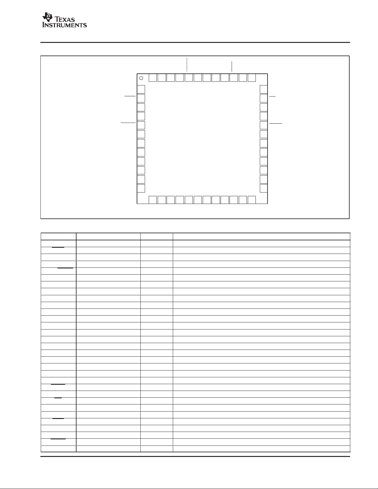
PIN CONFIGURATION
Top View QFN
DGND
DGND
CONV
DGND
DVA LID
DGND
CLK
DGND
DCLK
DCLK
DGND
DVDD
48 47 46 45 44 43 42
41 40 39 38
DOUT
DOUT
CLK_4X
FOR MA T
HISPD/LOPWR
RANG E0
RANG E1
RANG E2
AGND
VREF
AGND
AGND
1
2
3
4
5
6
7
8
9
10
11
12
13 14 15 16 17 18 19 20 21 22 233724
AIN8
AIN4
AGND
AIN7
DDC118
AIN3
AGND
AIN6
AGND
AIN2
AIN5
36
DIN
35
DIN
34
NC
33
NC
32
RESET
31
TEST
30
DGND
29
DGND
28
AGND
27
AVDD
26
AGND
25
AGND
AIN1
AGND
PIN DESCRIPTIONS
PIN NUMBER FUNCTION DESCRIPTION
DOUT 1 Digital Output Serial Data Output
DOUT 2 Digital Output Serial Data Output: Complementary Signal (optional, see text on page 13)
CLK_4X 3 Digital Input Master Clock Divider Control: 0 = divide by 1, 1 = divide by 4
FORMAT 4 Digital Input Digital Output Word Format: 0 = 16 Bits, 1 = 20 Bits
HISPD/LOPWR 5 Digital Input Mode Control: 0 = Low-Power, 1 = High-Speed
RANGE0 6 Digital Input Range Control 0 (least significant bit)
RANGE1 7 Digital Input Range Control 1
RANGE2 8 Digital Input Range Control 2 (most significant bit)
AGND 9, 11-13, 18, 19, 24-26, 28 Analog Analog Ground
VREF 10 Analog Input External Voltage Reference Input, 4.096V Nominal
AIN8 14 Analog Input Analog Input 8
AIN7 16 Analog Input Analog Input 7
AIN6 20 Analog Input Analog Input 6
AIN5 22 Analog Input Analog Input 5
AIN4 15 Analog Input Analog Input 4
AIN3 17 Analog Input Analog Input 3
AIN2 21 Analog Input Analog Input 2
AIN1 23 Analog Input Analog Input 1
AVDD 27 Analog Analog Power Supply, 5V Nominal
DGND 29, 30, 38, 41, 43, 45, 47, 48 Digital Digital Ground
TEST 31 Digital Input Test Mode Control
RESET 32 Digital Input Resets the Digital Circuitry, Active Low
NC 33, 34 — No connection. These pins must be left unconnected.
DIN 35 Digital Input Serial Data Input: Complementary Signal (optional, see text on page 13)
DIN 36 Digital Input Serial Data Input
DVDD 37 Digital Digital Power Supply, 3V Nominal
DCLK 39 Digital Input Serial Data Clock Input: Complementary Signal (optional, see text on page 13)
DCLK 40 Digital Input Serial Data Clock Input
CLK 42 Digital Input Master Clock Input
DVALID 44 Digital Output Data Valid Output, Active Low
CONV 46 Digital Input Conversion Control Input: 0 = Integrate on Side B, 1 = Integrate on Side A
5
Page 6
""#
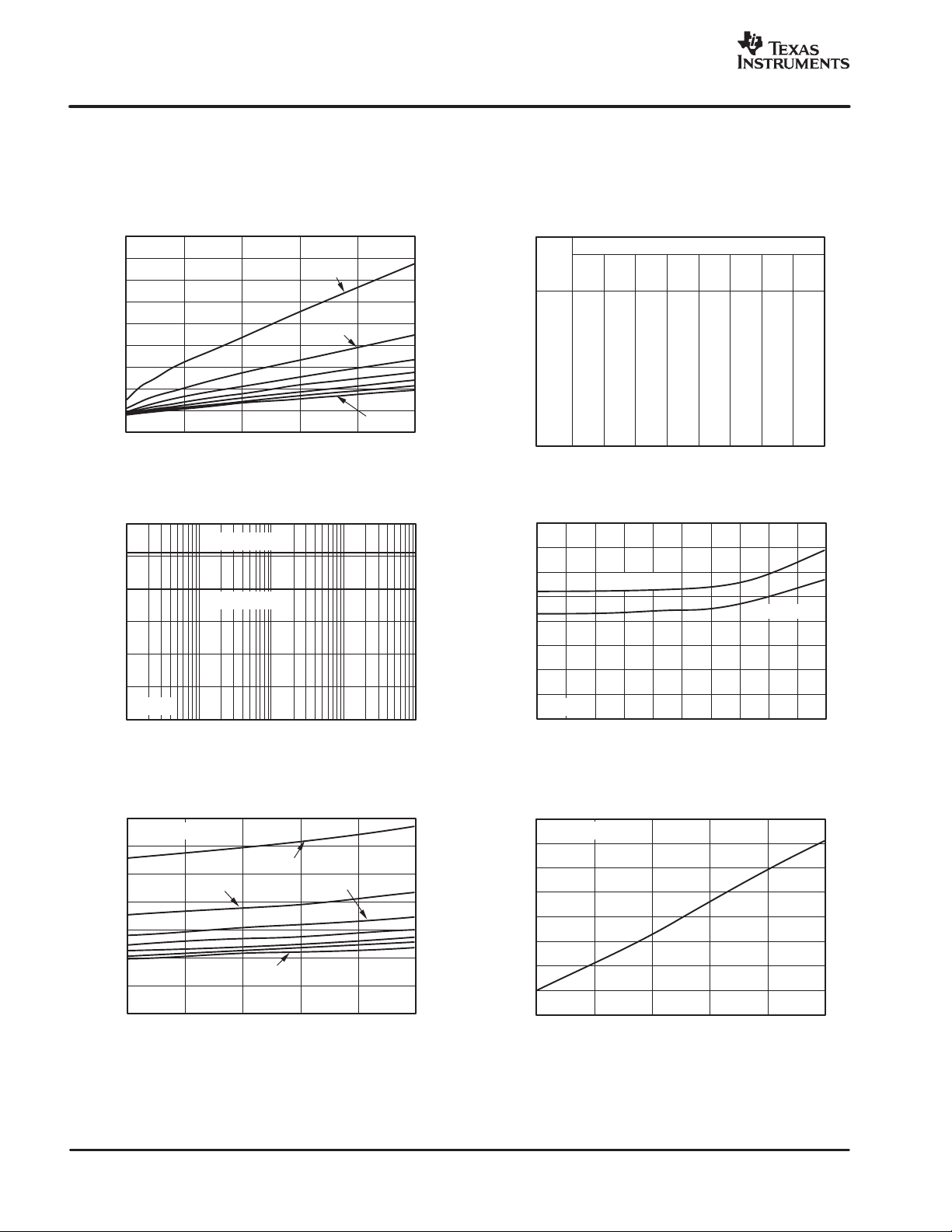
NOISE vs C
Range Drift (ppm)
SBAS325A − JUNE 2004 − REVISED JUNE 2005
TYPICAL CHARACTERISTICS
At TA = +25°C, characterization done with Range 5 (250pC), AVDD = +5V, DVDD = 3V, VREF = +4.096V, and Low-Power Mode: T
unless otherwise noted.
www.ti.com
= 400µs and CLK = 4MHz,
INT
45
NOISE vs C
40
35
30
25
20
15
10
Noise(ppmofFSR,rms)
5
0
100 4000 500300200
C
SENSOR
NOISE vs T
6
5
4
C
SENSOR
3
2
Noise (ppm of FSR, rms)
1
Range 5
0
1 10000.1 10010
C
SENSOR
= 50pF
T
=0pF
(ms)
INT
SENSOR
(pF)
INT
Range 1
Range 2
Range 7
SENSOR
Noise (ppmof FSR, rms)
C
SENSOR
(pF)
24
50
75
100
150
200
300
500
Range
Range
Range
5.2
6.7
8.2
8.9
10.0
11.9
13.5
16.3
22.4
Range
2
3
4.4
5.5
6.5
7.2
8.0
9.2
10.2
12.5
16.6
0
1
0
23.6
7.3
30.8
10.4
36.3
12.3
41.3
14.4
46.1
16.0
57.0
18.8
68.1
21.7
89.3
27.7
134.0
38.9
Range
4
4.2
4.9
5.6
6.0
6.7
7.8
8.6
10.6
13.5
Range
5
4.0
4.5
5.1
5.4
5.9
6.8
7.6
9.0
11.7
Range
6
3.8
4.3
4.8
5.1
5.4
6.1
6.8
8.1
10.4
Range
7
3.7
4.1
4.4
4.7
5.0
5.7
6.4
7.4
9.5
NOISE vs INPUT LEVEL
8
7
6
5
4
C
SENSOR
= 50pF
C
SENSOR
= 0pF
3
2
Noise (ppm of FSR, rms)
1
Range 5
0
20 3010 800 10060 70 9040 50
Input Level (% of Full−Scale)
14
C
=50pF
SENSOR
12
10
Range 2
Range 1
Range 3
8
2000
1500
1000
500
All Ranges
NOISE vs TEMPERATURE
RANGE DRIFT vs TEMPERATURE
0
6
4
Noise (ppm of FSR, rms)
2
Range 7
0
−
40
−
15 10 35 60 85
Temperature (_C)
−
−
−
−
500
1000
1500
2000
−
40
−
15 10 35 60 85
Temperature (_C)
6
Page 7
www.ti.com
IBvs TEMPERATURE
ANALOG SUPPLY CURRENTvs TEMPERATURE
POWER CONSUMPTION HISTOGRAM
OFFSET DRIFT vs TEMPERATURE
SBAS325A − JUNE 2004 − REVISED JUNE 2005
TYPICAL CHARACTERISTICS (continued)
At TA = +25°C, characterization done with Range 5 (250pC), AVDD = +5V, DVDD = 3V, VREF = +4.096V, and Low-Power Mode: T
unless otherwise noted.
""#
= 400µs and CLK = 4MHz,
INT
10
All Ranges
1
(pA)
B
I
0.1
0.01
25 35 45 55 65 75 85
Temperature (_C)
25
Low−Power Mode
20
15
10
Current (mA)
100
50
0
−
50
Offset Drift (ppm of FSR)
−
100
25 35 45 55 65 75 85
Temperature (_C)
2.5
2.0
1.5
1.0
Current (mA)
DIGITAL SUPPLY CURRENT vsTEMPERATURE
Low−Power Mode
DVDD= 5V
DVDD = 3V
5
0
−
40
40
35
30
25
20
15
Occurences(%)
10
5
0
−
15 10 35 60 85
Data collected
from multiple lots.
12.00
12.25
12.50
12.75
Temperature (_C)
13.00
13.25
13.50
13.75
14.00
Power per Channel (mW)
Low−Power Mode
14.25
14.50
14.75
15.00
15.25
15.50
15.75
16.00
Occurences
0.5
0
1200
1000
800
600
400
200
−
40
0
−
1.0
−
15 10 35 60 85
Temperature (_C)
OFFSET DRIFT HISTOGRAM AT ROOM TEMPERATURE
Repeated measurement
of offset drift over a
one minute interval.
−
0.6
−
0.2 0.2 0.6 1.0
Offset Drift (ppm of FSR/minute)
Range 5
7
Page 8
""#
SBAS325A − JUNE 2004 − REVISED JUNE 2005
www.ti.com
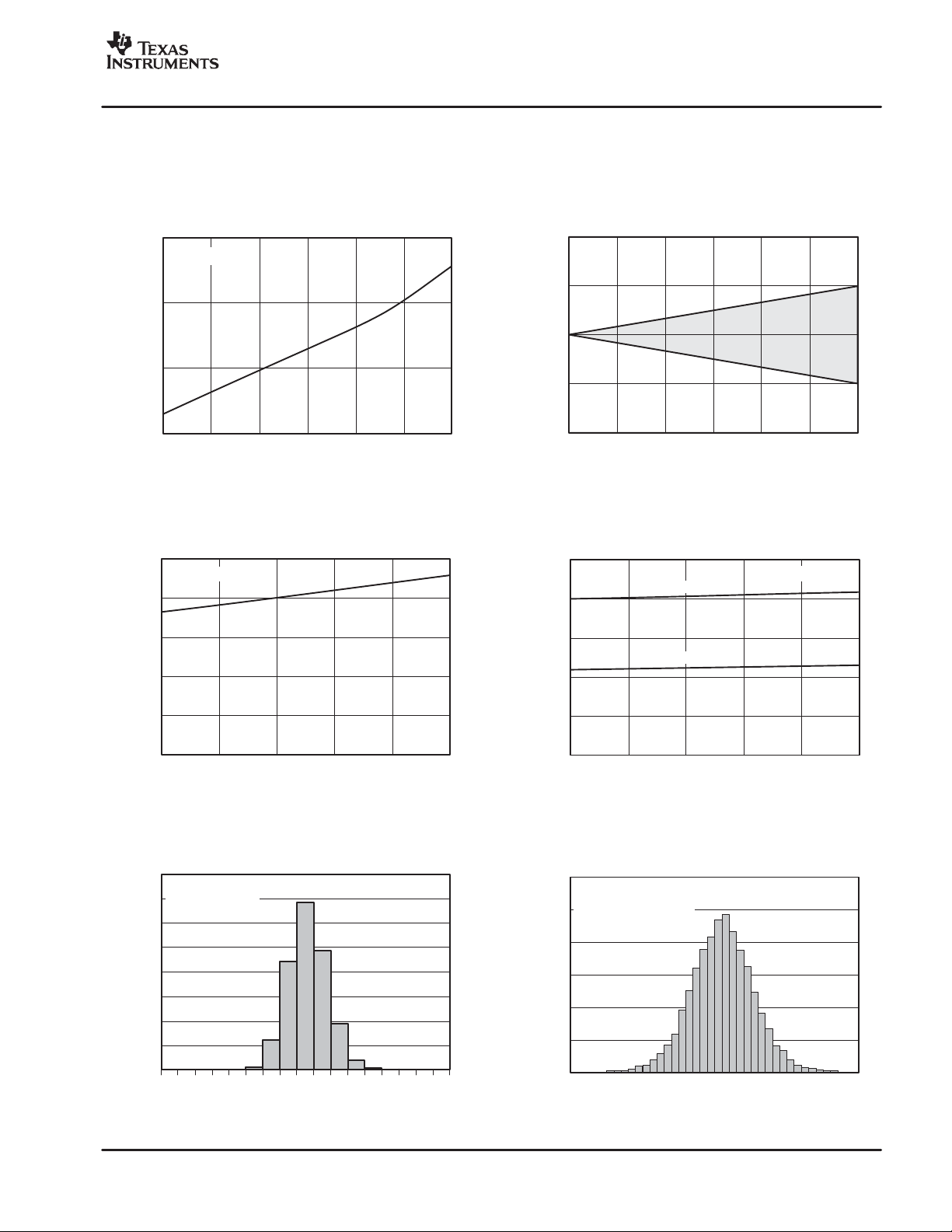
THEORY OF OPERATION
The block diagram of the DDC118 is shown in Figure 1.
The device contains eight identical input channels that
perform the function of current-to-voltage integration
followed by a multiplexed A/D conversion. Each input has
two integrators so that the current-to-voltage integration
can be continuous in time. The output of the sixteen
integrators are switched to four delta-sigma (∆Σ)
converters via four four-input multiplexers. With the
VREF
Modulator
Modulator
IN1
IN3
IN2
AVDD
Switched
Integrator
Switched
Integrator
Switched
Integrator
Dual
Dual
Dual
DDC118 in the continuous integration mode, the output of
the integrators from one side of the inputs will be digitized
while the other eight integrators are in the integration
mode, as illustrated in the timing diagram in Figure 2. This
integration and A/D conversion process is controlled by
the system clock, CLK. The results from side A and side
B of each signal input are stored in a serial output shift
register. The DVALID
output goes low when the shift
register contains valid data.
DVDD
CLK
CONV
RANGE0
∆Σ
∆Σ
Digital
Filter
Digital
Filter
Control
RANGE1
RANGE2
TEST
CLK_4X
HISPD/LOPWR
RESET
FORMAT
IN4
IN5
IN7
IN6
IN8
Dual
Switched
Integrator
Dual
Switched
Integrator
Dual
Switched
Integrator
Dual
Switched
Integrator
Dual
Switched
Integrator
AGND
∆Σ
Modulator
∆Σ
Modulator
Digital
Filter
Digital
Filter
DCLK
DCLK
DVALID
Digital
Input/Output
DOUT
DOUT
DIN
DIN
DGND
Figure 1. DDC118 Block Diagram
8
Page 9
www.ti.com
""#
SBAS325A − JUNE 2004 − REVISED JUNE 2005
The digital interface of the DDC118 provides the digital
results via a synchronous serial interface consisting of
differential data clocks (DCLK and DCLK), a valid data pin
(DVALID
DOUT
DIN
), differential serial data output pins (DOUT and
), and differential serial data input pins (DIN and
). The DDC118 contains only four A/D converters, so
the conversion process is interleaved (see Figure 2). The
integration and conversion process is fundamentally
independent of the data retrieval process. Consequently,
the CLK frequency and DCLK frequencies need not be the
same. DIN and DIN
are only used when multiple
converters are cascaded and should be tied to DGND and
DVDD otherwise.
DEVICE OPERATION
Basic Integration Cycle
The topology of the front end of the DDC118 is an analog
integrator as shown in Figure 3. In this diagram, only Input
IN1 is shown. This representation of the input stage
consists of an operational amplifier, a selectable feedback
capacitor network (C
IN1, IN2, IN5, and IN6,
IN1, IN2, IN5, and IN6,
IN3, IN4, IN7, and IN8,
IN3, IN4, IN7, and IN8,
Conversion in Progress
Integrator A
Integrator B
Integrator A
Integrator B
DVALID
), and several switches that
F
Integrate
Integrate
IN1B
IN2B
IN5B
IN6B
IN3B
IN4B
IN7B
IN8B
IN1A
IN2A
IN5A
IN6A
implement the integration cycle. The timing relationships
of all of the switches shown in Figure 3 are illustrated in
Figure 4. Figure 4 is used to conceptualize the operation
of the integrator input stage of the DDC118 and should not
be used as an exact timing tool for design. See Figure 5 for
the block diagrams of the reset, integrate, wait and convert
states of the integrator section of the DDC118. This
internal switching network is controlled externally with the
convert pin (CONV), range selection pins
(RANGE0-RANGE2), and the system clock (CLK). For the
best noise performance, CONV must be synchronized
with the rising edge of CLK. It is recommended that CONV
toggle within ±10ns of the rising edge of CLK.
The noninverting inputs of the integrators are connected to
ground. Consequently, the DDC118 analog ground should
be as clean as possible. The range switches, along with
the internal and external capacitors (C
), are shown in
F
parallel between the inverting input and output of the
operational amplifier. At the beginning of a conversion, the
switches S
A/D
, S
INTA
, S
INTB
, S
REF1
, S
REF2
are set (see Figure 4).
Integrate
IN1A
IN2A
IN5A
IN6A
Integrate
Integrate
IN3A
IN4A
IN7A
IN8A
Integrate
Integrate
IN3A
IN4A
IN7A
IN8A
IN1B
IN2B
IN5B
IN6B
Integrate
IN3B
IN4B
IN7B
IN8B
, and S
RESET
Figure 2. Basic Integration and Conversion Timing for the DDC118 (continuous mode)
S
Photodiode
Input
Current
IN1
ESD
Protection
Diodes
REF1
3pF
50pF
25pF
12.5pF
S
INTA
S
RESET
S
INTB
Integrator A
IntegratorB (same asA)
S
S
REF2
A/D1A
VREF
RANGE2
RANGE1
RANGE0
To Converter
Figure 3. Basic Integration Configuration for Input 1, shown with a 250pC (CF = 62.5pF) Input Range
9
Page 10

""#
SBAS325A − JUNE 2004 − REVISED JUNE 2005
CONV
CLK
S
INTA
S
INTB
S
REF1
S
REF2
S
RESET
S
A/D1A
www.ti.com
Configuration of
Integrator A
VREF
Integrator A
Voltage Output
S
INT
IN
S
RESET
a) Reset Configuration
S
INT
IN
S
RESET
c) Integrate Configuration
WaitConvert WaitConvertIntegrate
Wait
Reset
Figure 4. Basic Integration Timing Diagram (as shown in Figure 3)
S
S
REF2
REF2
S
S
S
S
REF1
A/D
REF1
A/D
VREF
To Converter
VREF
To Converter
S
INT
IN
S
RESET
b) Wait Configuration
S
INT
IN
S
RESET
S
S
S
REF2
REF2
C
F
C
F
C
F
C
F
REF1
S
S
S
A/D
REF1
A/D
Wait
Reset
VREF
To Converter
VREF
To Converter
10
d) Convert Configuration
Figure 5. Diagrams for the Four Configurations of the Front End Integrators of the DDC118
Page 11

www.ti.com
""#
SBAS325A − JUNE 2004 − REVISED JUNE 2005
At the completion of an A/D conversion, the charge on the
integration capacitor (C
) is reset with S
F
REF1
and S
RESET
(see Figure 4 and Figure 5a). In this manner, the selected
capacitor is charged to the reference voltage, VREF. Once
the integration capacitor is charged, S
REF1
and S
RESET
are switched so that VREF is no longer connected to the
amplifier circuit while it waits to begin integrating (see
Figure 5b). With the rising edge of CONV, S
INTA
closes,
which begins the integration of side A. This process puts
the integrator stage into its integrate mode (see Figure 5c).
Charge from the input signal is collected on the integration
capacitor, causing the voltage output of the amplifier to
decrease. The falling edge of CONV stops the integration
by switching the input signal from side A to side B (S
and S
). Prior to the falling edge of CONV, the signal on
INTB
INTA
side B was converted by the A/D converter and reset
during the time that side A was integrating. With the falling
edge of CONV, side B starts integrating the input signal.
Now the output voltage of the side A operational amplifier
is presented to the input of the ∆Σ A/D converter (see
Figure 5d).
Integration Capacitors
There are eight different capacitors available on-chip for
both sides of every channel in the DDC118. These internal
capacitors are trimmed in production to achieve the
specified performance for range error of the DDC118. The
range control pins (RANGE0-RANGE2) change the
capacitor value for all four integrators. Consequently, all
inputs and both sides of each input will always have the
same full-scale range. Table 1 shows the capacitor value
selected for each range selection.
Table 1. Range Selection of the DDC118
C
RANGE2 RANGE1 RANGE0
0 0 0 3 −0.048 to 12
0 0 1 12.5 –0.2 to 50
0 1 0 25 –0.4 to 100
0 1 1 37.5 –0.6 to 150
1 0 0 50 –0.8 to 200
1 0 1 62.5 –0.1 to 250
1 1 0 75 –1.2 to 300
1 1 1 87.5 –1.4 to 350
F
(pF, typ)
INPUT RANGE
(pC, typ)
Voltage Reference
The external voltage reference is used to reset the
integration capacitors before an integration cycle begins.
It is also used by the ∆Σ converter while the converter is
measuring the voltage stored on the integrators after an
integration cycle ends. During this sampling, the external
reference must supply the charge needed by the ∆Σ
converter. For an integration time of 400µs, this charge
translates to an average VREF current of approximately
150µA. The amount of charge needed by the ∆Σ converter
is independent of the integration time; therefore,
increasing the integration time lowers the average current.
For example, an integration time of 800µs lowers the
average VREF current to 75µA.
It is critical that VREF be stable during the different modes
of operation (see Figure 5). The ∆Σ converter measures
the voltage on the integrator with respect to VREF. Since
the integrator capacitors are initially reset to VREF, any
drop in VREF from the time the capacitors are reset to the
time when the converter measures the integrator output
will introduce an offset. It is also important that VREF be
stable over longer periods of time because changes in
VREF correspond directly to changes in the full-scale
range. Finally, VREF should introduce as little additional
noise as possible.
For these reasons, it is strongly recommended that the
external reference source be buffered with an operational
amplifier, as shown in Figure 6. In this circuit, the voltage
reference is generated by a 4.096V reference.
A low-pass
filter to reduce noise connects the reference to an
operational amplifier configured as a buffer . This amplifier
should have low noise, and input/output common-mode
ranges that support VREF. Following the buffer are
capacitors placed close to the DDC118 VREF pin. Even
though the circuit in Figure 6 might appear to be unstable
because of the large output capacitors, it works well for
most operational amplifiers. It is NOT recommended that
series resistance be placed in the output lead to improve
stability since this can cause a drop in VREF, which
producing large offsets.
2
3
+5V
0.10µF
7
OPA350
4
6
+
10µF
To VREF
Pin10of
the DDC118
0.1µF
0.47µF
REF3140
+5V
1
Ω
10k
2
+
3
10µF
0.10µF
Figure 6. Recommended External Voltage Reference Circuit for Best Low-Noise Operation with the DDC118
11
Page 12

""#
SBAS325A − JUNE 2004 − REVISED JUNE 2005
www.ti.com
DDC118 Frequency Response
The frequency response of the DDC118 is set by the front
end integrators and is that of a traditional continuous time
integrator, as shown in Figure 7. By adjusting T
INT
, the
user can change the 3dB bandwidth and the location of the
notches in the response. The frequency response of the
∆Σ converter that follows the front end integrator is of no
consequence because the converter samples a held
signal from the integrators. That is, the input to the ∆Σ
converter is always a DC signal. Since the output of the
front end integrators are sampled, aliasing can occur.
Whenever the frequency of the input signal exceeds
one-half of the sampling rate, the signal will fold back down
to lower frequencies.
0
−
10
−
20
−
30
Gain (dB)
−
40
Test Mode
When Test Mode is used, the inputs (IN1, IN2, IN3, IN4,
IN5, IN6, IN7, and IN8) are disconnected from the DDC1 18
integrators to enable the user to measure a zero input
signal regardless of the current supplied to the inputs. In
addition, packets of charge can be transferred to the
integrators in 11pC intervals to measure non-zero values.
The test mode works with both the continuous and
non-continuous modes. The timing diagram for the test
mode is shown in Figure 8 with the timing specifications
given in Table 2.
To enter Test Mode, hold TEST high while CONV
transitions. If TEST is held high during the entire
integration period, the integrators measure a zero value.
This mode can be used to help debug a design or perform
diagnostic tests. To apply packets of charge during Test
Mode, simply strobe TEST low then high before the next
CONV transition. Each rising edge of TEST causes
approximately 11pC of charge to be transferred to the
integrators. This charge transfer is independent of the
integration time. Data retrieval during Test Mode is
identical to normal operation. To exit Test Mode, take
TEST low and allow several cycles after exiting before
using the data.
−
50
0.1
T
INT
T
1
INT
Frequency
10
T
INT
100
T
INT
Figure 7. Frequency Response of the DDC118
Action
CONV
TEST
Test Mode D isabled
Integrate B Integrate A
0pC into B 11pC into A 22pC into B 33pC into A
t
4
t
1
t
3
t
6
t
5
Test Mode DisabledTest Mode Enabled: Inputs Disconnected
Integrate B Integrate A
t
2
t
4
Figure 8. Timing Diagram of the Test Mode of the DDC118
Table 2. Timing for the DDC118 in the Test Mode
SYMBOL DESCRIPTION MIN TYP MAX UNITS
t
1
t
2
t
3
t
4
t
5
t
6
From Rising Edge of TEST to the Edge of CONV while Test Mode
Setup Time for Test Mode Enable 100 ns
Setup Time for Test Mode Disable 100 ns
Hold Time for Test Mode Enable 100 ns
Enabled
Falling Edge to Rising Edge of TEST 1 µs
Rising Edge to Falling Edge of TEST 1 µs
1 µs
12
Page 13

www.ti.com
""#
SBAS325A − JUNE 2004 − REVISED JUNE 2005
DIGITAL INTERFACE
The digital interface of the DDC118 provides the digital
results via a synchronous serial interface consisting of
differential data clocks (DCLK and DCLK), a valid data pin
(DVALID
DOUT
DIN
the conversion process is interleaved (see Figure 2,
page 9). The integration and conversion processes are
independent of the data retrieval process. Consequently,
the CLK frequency and DCLK frequencies need not be the
same. DIN and DIN
cascaded. Cascading or daisy-chaining greatly simplifies
the interconnection and routing of the digital outputs in
cases where a large number of converters are needed.
Refer to the Cascading Multiple Converters section of this
data sheet for more detail.
Complementary Signals (DCLK, DIN, and DOUT)
The DDC118 provides optional complementary inputs
(DCLK
inputs. If using these inputs, connect a complementary
signal to each. If these inputs are not connected on the
DDC118, they should be tied to DGND. DOUT
complementary output designed to drive DIN
DOUT
System and Data Clocks (CLK and CONV)
The system clock is supplied to CLK and the data clock is
supplied to DCLK. Make sure the clock signals are
clean—avoid overshoot or ringing. For best performance,
generate both clocks from the same clock source. DCLK
should be disabled by taking it low after the data has been
shifted out or while CONV is transitioning.
When using multiple DDC118s, pay close attention to the
DCLK distribution on the printed circuit board (PCB). In
particular, make sure to minimize skew in the DCLK signal
as this can lead to timing violations in the serial interface
specifications. See the Cascading Multiple Converters
section for more details.
), differential serial data output pins (DOUT and
), and differential serial data input pins (DIN and
). The DDC118 contains only four A/D converters, so
are used when multiple converters are
, DIN) to help reduce digital coupling to the analog
is a
. If not using
, leave it floating.
High-Speed and Low-Power Modes
(HISPD/LOPWR
)
The HISPD/LOPWR input controls the power dissipation
and in turn, the maximum allowable CLK frequency and
data rate, as shown in Table 4. With HISPD/LOPWR
= 0,
the Low-Power Mode is selected with a typical 13.5mW/
channel and a maximum data rate of 2.5kSPS. Setting
HISPD/LOPWR
= 1 selects the High-Speed Mode, which
supports a maximum data rate of 3.125kSPS with a corresponding typical power of 18.0mW/channel.
Table 4. HISPD/LOPWR Pin Operation
HISPD/
LOPWR
0 Low-Power 13.5mW/ch 4.0MHz 2.5kSPS
1 High-Speed 18.0mW/ch 4.8MHz 3.125kSPS
MODE
TYPICAL
POWER/
CHANNEL
MAXIMUM
CLK FREQUENCY
(CLK_4X = 0)
MAXIMUM
DATA
RATE
Data Valid (DVALID)
The DVALID signal indicates that data is ready. Data
retrieval may begin after DVALID
goes low. This signal is
generated using an internal clock divided down from the
system clock CLK. The phase relationship between this
internal clock and CLK is set when power is first applied
and is random. Since the user must synchronize CONV
with CLK, the DVALID
relationship with CONV. This uncertainty is ± 1/f
Polling DVALID
signal will have a random phase
CLK
eliminates any concern about this
relationship. If data read back is timed from CONV, wait the
maximum value of t
or t8 to insure data is valid.
7
Reset (RESET)
The DDC118 is reset asynchronously by taking the
RESET
input low, as shown in Figure 9. Make sure the
reset pulse is at least 50µs wide. After resetting the
DDC118, wait at least four conversions before using the
data. It is very important to make sure the RESET
free to avoid unintended resets. The RESET
is glitch
pin is used
during power-up; see the Power-Up Sequence section for
more details.
.
System Clock Divider (CLK_4X)
The CLK_4X input enables an internal divider on the
system clock as shown in Table 3. When CLK_4X = 1, the
system clock is divided by four. This allows a 4X faster
system clock, which in turn provides a finer quantization of
the integration time as the CONV signal needs to be
synchronized with the system clock for the best
performance.
Table 3. CLK_4X Pin Operation
CLK_4X
PIN
0 1 4MHz 4MHz
1 4 16MHz 4MHz
CLK DIVIDER
VALUE
TYPICAL CLK
FREQUENCY
INTERNAL CLOCK
FREQUENCY
RESET
>50µs
Figure 9. Reset Timing
Convert (CONV)
CONV controls the integration time (T
). For optimum
INT
analog performance, make sure CONV is synchronized to
CLK.
This recommendation implies that while SPEED is low,
needs to be adjusted in steps of 250ns if CLK_4X is
T
INT
low and CLK = 4MHz. If CLK_4X is high and CLK =
16MHz, this allows T
to be adjusted in steps of 62.5ns.
INT
13
Page 14

""#
SBAS325A − JUNE 2004 − REVISED JUNE 2005
Conversion Rate
The conversion rate of the DDC118 is set by a combination
of the integration time (determined by the user) and the
speed of the A/D conversion process. The A/D conversion
time is primarily a function of the system clock (CLK)
speed. One A/D conversion cycle encompasses the
conversion of two signals (one side of each dual integrator
feeding the modulator) and the reset time for each of the
integrators involved in the two conversions. In most
situations, the A/D conversion time is shorter than the
integration time. If this condition exists, the DDC118 will
operate in the continuous mode. When the DDC118 is in
the continuous mode, the sensor output is continuously
integrated by one of the two sides of each input.
CONV× mbsy
IntB/Meas A
1
Ncont
4
Cont
CONV|mbsy
CONV
CONV × mbsy
3
Int A
Cont
CONV× mbsy
CONV× mbsy
www.ti.com
2
Ncont
CONV
5
Int A/Meas B
Cont
In the event that the A/D conversion takes longer than the
integration time, the DDC118 will switch into a
non-continuous mode. In non-continuous mode, the A/D
converter is not able to keep pace with the speed of the
integration process. Consequently, the integration
process is periodically halted until the digitizing process
catches up. These two basic modes of operation for the
DDC118—continuous and non-continuous modes—are
described below.
Continuous and Non-Continuous Operational
Modes
Figure 10 shows the state diagram of the DDC118. In all,
there are eight states. Table 5 provides a brief explanation
of each state.
Table 5. State Descriptions
STATE MODE DESCRIPTION
1 Ncont Complete m/r/az of side A, then side B (if previous
state is state 4). Initial power-up state when CONV
is initially held HIGH.
2 Ncont Prepare side A for integration.
3 Cont Integrate on side A.
4 Cont Integrate on side B; m/r/az on side A.
5 Cont Integrate on side A; m/r/az on side B.
6 Cont Integrate on side B.
7 Ncont Prepare side B for integration.
8 Ncont Complete m/r/az of side B, then side A (if previous
state is state 5). Initial power-up state when CONV
is initially held LOW.
Four signals are used to control progression around the
state diagram: CONV, mbsy, and their complements. The
state machine uses the level as opposed to the edges of
CONV to control the progression. mbsy is an internallygenerated signal not available to the user. It is active
whenever a measurement/reset/auto-zero (m/r/az) cycle
is in progress.
CONV
CONV × mbsy
8
Ncont
CONV|mbsy
7
Ncont
6
Int B
Cont
CONV
CONV × mbsy
Figure 10. Integrate/Measure State Diagram
During the cont mode, mbsy is not active when CONV
toggles. The non-integrating side is always ready to begin
integrating when the other side finishes its integration.
Consequently, monitoring the current status of CONV is all
that is needed to know the current state. Cont mode
operation corresponds to states 3-6. Two of the states, 3
and 6, only perform an integration (no m/r/az cycle).
mbsy becomes important when operating in the ncont
mode, states 1, 2, 7, and 8. Whenever CONV is toggled
while mbsy is active, the DDC118 will enter or remain in
either ncont state 1 (or 8). After mbsy goes inactive, state
2 (or 7) is entered. This state prepares the appropriate side
for integration. In the ncont states, the inputs to the
DDC118 are grounded.
One interesting observation from the state diagram is that
the integrations always alternate between sides A and B.
This relationship holds for any CONV pattern and is
independent of the mode. States 2 and 7 insure this
relationship during the ncont mode.
When power is first applied to the DDC118, the beginning
state is either 1 or 8, depending on the initial level of CONV.
For CONV held high at power-up, the beginning state is 1.
Conversely, for CONV held low at power-up, the beginning
state is 8. In general, there is a symmetry in the state
diagram between states 1-8, 2-7, 3-6, and 4-5. Inverting
CONV results in the states progressing through their
symmetrical match.
14
Page 15

www.ti.com
""#
SBAS325A − JUNE 2004 − REVISED JUNE 2005
TIMING EXAMPLES
Cont Mode
A few timing diagrams help illustrate the operation of the
state machine. These diagrams are shown in Figure 11
through Figure 19. Table 6 gives generalized timing
specifications in units of CLK periods for CLK_4X = 0. If
CLK_4X = 1, these values increase by a factor of four
because of the internal clock divider. Values (in µs) for
Table 6 can be easily found for a given CLK. For example,
if CLK = 4MHz, then a CLK period = 0.25µs. t
would then be 367.50 ± 0.125µs.
Table 6. Timing Specifications Generalized in
CLK Periods
SYMBOL DESCRIPTION
t
Cont mode m/r/az cycle 1470 ± 0.5
6
t
Cont mode data ready 1380 ± 0.5
7
t
1st ncont mode data ready 1379 ± 1
8
t
2nd ncont mode data ready 1450
9
t
Ncont mode m/r/az cycle 2901 ± 1
10
VALUE
(CLK periods with CLK_4X = 0)
Figure 11 shows a few integration cycles beginning with
initial power-up for a cont mode example. The top signal
is CONV and is supplied by the user. The next line
indicates the current state in the state diagram. The
following two traces show when integrations and
in Table 6
6
measurement cycles are underway. The internal signal
mbsy is shown next. Finally, DVALID
is given. DVALID
goes active low when data is ready to be retrieved from the
DDC118. It stays low until DCLK is taken high and then
back low by the user. The text below the DVALID
pulse
indicates the side of the data available to be read, and
arrows help match the data to the corresponding
integration. The signals illustrated in Figure 11 through
Figure 19 are drawn at approximately the same scale.
In Figure 11, the first state is ncont state 8. The DDC118
always powers up in the ncont mode. In this case, the first
state is 8 because CONV is initially low. After the first two
states, cont mode operation is reached and the states
begin toggling between 4 and 5. From now on, the input is
being continuously integrated, either on side A or side B.
The time needed for the m/r/az cycle, or t
, is the same time
6
that determines the boundary between the cont and ncont
modes described earlier in the Overview section. DVALID
goes low after CONV toggles in time t7, indicating that data
is ready to be retrieved. As shown in Figure 11, there are
two values for t
and t7. The reason for this is discussed in
6
the Special Considerations section.
See Figure 12 for the timing diagram of the internal
operations occurring during continuous mode operation.
Table 7 gives the timing specifications in the continuous
mode.
CONV
State
Integration
Status
m/r/az
Status
mbsy
DVALID
t=0
Power− Up
SYMBOL DESCRIPTION VALUE (CLK = 4MHz, CLK_4X = 0) VALUE (CLK = 4.8MHz, CLK_4X = 0)
t
6
t
7
Cont Mode m/r/az Cycle 367.50 ± 0.125µs 306.25 ± 0.104µs
Cont Mode Data Ready 345.00 ± 0.125µs 287.5 ± 0.104µs
5678 45
Integrate AIntegrate B Integrate B Integrate A
m/r/az B m/r/az A m/r/az B
t
6
t
7
Side B
Data
Side A
Data
Side B
Data
Figure 11. Continuous Mode Timing
15
Page 16

""#
SBAS325A − JUNE 2004 − REVISED JUNE 2005
www.ti.com
Inputs 1, 2, 5, and 6(Internal)
A/D Conversion
A/D Conversion
Inputs 3, 4, 7, and 8(Internal)
Figure 12. Timing Diagram of the Internal Operation in Continuous Mode of the DDC118
SYMBOL DESCRIPTION
T
Integration Period (continuous mode) 400 1,000,000 320 1,000,000 µs
INT
t
A/D Conversion Time (internally controlled) 169.5 141.25 µs
12
t
A/D Conversion Reset Time (internally controlled) 4 3.333 µs
13
Integrator and A/D Conversion Reset Time
t
14
(internally controlled)
EndIntegrationSide A
Start Integration Side B
CONV
Side A
t
12
t
T
INT
SideA
t
13
End Integration Side B
Start Integration Side A
12
T
INT
Side B
t
13
t
14
SideB
DVALID
Side A
Data Ready
Side B
Data Ready
Table 7. Timing for the Internal Operation in Continuous Mode
CLK = 4MHz, CLK_4X = 0 CLK = 4.8MHz, CLK_4X = 0
MIN TYP MAX MIN TYP MAX
23 19.167 µs
End Integration Side A
Start Integration Side B
t
14
SideA
UNITS
16
Page 17

www.ti.com
""#
SBAS325A − JUNE 2004 − REVISED JUNE 2005
Ncont Mode
Non-continuous mode of operation is intended for Ranges
1 to 7. It is not recommended to use Range 0 when
operating in non-continuous mode. Figure 13 illustrates
operation in the ncont mode. The integrations come in
pairs (that is, sides A/B or sides B/A) followed by a time
during which no integrations occur. During that time, the
previous integrations are being measured, reset and
auto-zeroed. Before the DDC1 18 can advance to states 3
or 6, both sides A and B must be finished with the m/r/az
cycle which takes time t
completed, time t
is needed to prepare the next side for
11
. When the m/r/az cycles are
10
integration. This time is required for the ncont mode
because the m/r/az cycle of the ncont mode is slightly
different from that of the cont mode. After the first
CONV
State
Integration
Status
integration ends, DV ALID
goes low in time t8. This time is
the same as in the cont mode. The second data will be
ready in time t9 after the first data is ready . One res ult o f the
naming convention used in this data sheet is that when the
DDC118 is operating in the ncont mode, it passes through
both ncont mode states and cont mode states. For
example, in Figure 13, the state pattern is 3, 4, 1, 2, 3, 4,
1, 2, 3, 4 ... where 3 and 4 are cont mode states. Ncont
mode, by definition, means that for some portion of the
time, neither side A nor B is integrating. States that perform
an integration are labeled cont mode states, while those
that do not are called ncont mode states. Since
integrations are performed in the ncont mode, just not
continuously, some cont mode states must be used in a
ncont mode state pattern.
23134 4 1 2
t
11
Int BInt AInt BInt A
m/r/az
Status
mbsy
DVALID
t
8
Side A
Data
SYMBOL DESCRIPTION VALUE (CLK = 4MHz, CLK_4X = 0) VALUE (CLK = 4.8MHz, CLK_4X = 0)
t
8
t
9
t
10
t
11
1st ncont Mode Data Ready 344.75 ± 0.25µs 287.292 ± 0.208µs
2nd ncont Mode Data Ready 362.5µs 302.083µs
ncont Mode m/r/az Cycle 725.25 ± 0.25µs 604.375 ± 0.208µs
Prepare Side for Integration ≥ 18µs ≥ 15µs
m/r/az Bm/r/az A
t
10
t
9
Side B
Data
m/r/az A m/r/az B
Side A
Data
SideB
Data
Figure 13. Non-Continuous Mode Timing
17
Page 18

""#
SYMBOL
DESCRIPTION
UNITS
SBAS325A − JUNE 2004 − REVISED JUNE 2005
www.ti.com
CONV
A/D Conversion
Inputs 1, 2, 5, and 6
Start Integration Side A
End Integration Side A
StartIntegration Side B
T
INT
End Integration Side B
WaitState
T
INT
t
12
t
16
Start Integration Side A
Release
State
t
17
A/D Conversion
Inputs 3, 4, 7, and 8
t
13
t
12
t
15
DVALID
Side A
Data Ready
Side B
Data Ready
Figure 14. Conversion Detail for the Internal Operation of Non-Continuous Mode with Side A Integrated
First
Table 8. Internal Timing for the DDC118 in Non-Continuous Mode
CLK = 4MHz, CLK_4X = 0 CLK = 4.8MHz, CLK_4X = 0
MIN TYP MAX MIN TYP MAX
T
Integration Time (non-continuous mode) 400 1,000,000 320 1,000,000 µs
INT
t
A/D Conversion Time (internally controlled) 169.5 141.25 µs
12
t
A/D Conversion Reset Time (internally controlled) 4 3.333 µs
13
Integrator and A/D Conversion Reset Time
t
15
(internally controlled)
t
Total A/D Conversion and Reset Time (internally controlled) 725.25 ± 0.25 604.375 ± 0.208 µs
16
t
Release Time 18 15 µs
17
19.5 16.25 µs
CONV
A/D Conversion
Inputs 1, 2, 5, and 6
Start Integration Side A
End Integration Side A
StartIntegration Side B
T
INT
End Integration Side B
WaitState
T
INT
t
12
t
16
Start Integration Side A
Release
State
t
17
A/D Conversion
Inputs 3, 4, 7, and 8
t
13
t
12
t
15
DVALID
Side A
Data Ready
Side B
Data Ready
Figure 15. Internal Operation Timing Diagram of Non-Continuous Mode with Side B Integrated First
18
Page 19

www.ti.com
""#
SBAS325A − JUNE 2004 − REVISED JUNE 2005
Looking at the state diagram, one can see that the CONV
pattern needed to generate a given state progression is not
unique. Upon entering states 1 or 8, the DDC1 18 remains
in those states until mbsy goes low, independent of CONV.
As long as the m/r/az cycle is underway , the state machine
ignores CONV (see Figure 10, page 14). The top two
signals in Figure 16 are different CONV patterns that
produce the same state. This feature allows flexibility in
generating ncont mode CONV patterns. For example, the
DDC118 Evaluation Fixture operates in the ncont mode by
generating a square wave with pulse width < t
. Figure 17
6
illustrates operation in the ncont mode using a 50% duty
CONV1
CONV2
mbsy
State
cycle CONV signal with T
= 512 CLK periods. Care
INT
must be exercised when using a square wave to generate
CONV. There are certain integration times that must be
avoided since they produce very short intervals for state 2
(or state 7 if CONV is inverted). As seen in the state
diagram, the state progresses from 2 to 3 as soon as
CONV is high. The state machine does not insure that the
duration of state 2 is long enough to properly prepare the
next side for integration (t
). This must be done by the
11
user with proper timing of CONV. For example, if CONV is
a square wave with T
only be 9 CLK periods long; therefore, t
23134 4 1 2
= 970 CLK periods, state 2 will
INT
will not be met.
11
CONV
State
Integration
Status
mbsy
DVALID
Figure 16. Equivalent CONV Signals in Non-Continuous Mode
23134 41
IntA
SideA
Data
Side B
Data
Int BInt AIntB
Figure 17. Non-Continuous Mode Timing with a 50% Duty Cycle CONV Signal
Side A
Data
19
Page 20

""#
SBAS325A − JUNE 2004 − REVISED JUNE 2005
www.ti.com
Changing Between Modes
Changing from the cont to ncont mode occurs whenever
< t6. Figure 18 shows an example of this transition.
T
INT
In this figure, the cont mode is entered when the integration
on side A is completed before the m/r/az cycle on side B
is complete. The DDC118 completes the measurement on
sides B and A during states 8 and 7 with the input signal
shorted to ground. Ncont integration begins with state 6.
CONV
State
Integration
Status
m/r/az
Status
5 65
Continuous Non−Continuous
Integrate A Integrate B Int AInt A Int B
m/r/az B m/r/az A m/r/az B m/r/az A m/r/az B
Changing from the ncont to cont mode occurs when T
is increased so that T
is always ≥ t6, as shown in
INT
INT
Figure 19 (see also Figure 14 and Table 8, page 18). With
a longer T
, the m/r/az cycle has enough time to finish
INT
before the next integration begins and continuous
integration of the input signal is possible. For the special
case of the very first integration when changing to the cont
mode, T
no simultaneous
can be < t6. This is allowed because there is
INT
m/r/az cycle on the side B during state
3—there is no n e e d t o w a i t f or it to fi n ish before ending the
integration on side A.
8745
CONV
State
Integration
Status
m/r/az
Status
mbsy
mbsy
Figure 18. Changing from Continuous Mode to Non-Continuous Mode
33
Non−Continuous Continuous
Int BInt A Integrate A Integrate B
m/r/az A m/r/az B m/r/az A
Figure 19. Changing from Non-Continuous Mode to Continuous Mode
4214
20
Page 21

www.ti.com
SYMBOL
DESCRIPTION
UNITS
""#
SBAS325A − JUNE 2004 − REVISED JUNE 2005
DATA FORMAT (FORMAT)
The serial output data is provided in an offset binary code
as shown in Table 9. The digital input pin FORMAT selects
how many bits are used in the output word. When
FORMAT is high (1), 20 bits are used. When FORMAT is
low (0), the lower 4 bits are truncated so that only 16 bits
are used. Note that the LSB size is 16 times bigger when
FORMAT = 0. An offset is included in the output to allow
slightly negative inputs, from board leakages for example,
from clipping the reading. This offset is approximately
0.4% of the positive full-scale.
Table 9. Ideal Output Code
INPUT
SIGNAL
≥ 100% FS 1111 1111 1111 1111 1111 1111 1111 1111 1111
0.001531% FS 0000 0001 0000 0001 0000 0000 0001 0000 0001
0.001436% FS 0000 0001 0000 0000 1111 0000 0001 0000 0000
0.000191% FS 0000 0001 0000 0000 0010 0000 0001 0000 0000
0.000096% FS 0000 0001 0000 0000 0001 0000 0001 0000 0000
0% FS 0000 0001 0000 0000 0000 0000 0001 0000 0000
−0.3955% FS 0000 0000 0000 0000 0000 0000 0000 0000 0000
(1)
Excludes the effects of noise, INL, offset, and gain errors.
IDEAL OUTPUT CODE
FORMAT = HIGH (1)
(1)
vs Input Signal
IDEAL OUTPUT CODE
FORMAT = LOW (0)
DATA RETRIEVAL
In both the continuous and non-continuous modes of
operation, the data from the last conversion is available for
retrieval on the falling edge of DVALID
Table 10). Data is shifted out on the falling edge of the data
clock, DCLK. Make sure not to retrieve data while CONV
changes as this can introduce noise. Stop activity on
DCLK at least 10µs before or after a CONV transition.
Setting the FORMAT pin = 0 (16-bit output word) reduces
the time needed to retrieve data by 20%, since there are
fewer bits to shift out. This time reduction can be useful in
multichannel systems requiring only 16 bits of resolution.
(see Figure 20 and
CLK
t
18
DVA LID
t
DCLK
DOUT
20
Input 8
MSB
t
19
t
21
Input 8
LSB
Input 7
MSB
Input 5
LSB
Figure 20. Digital Interface Timing Diagram for Data Retrieval From a Single DDC118
Table 10. Timing for the DDC118 Data Retrieval
t
Propagation Delay from Falling Edge of CLK to DVALID LOW 5 5 ns
18
t
Propagation Delay from Falling Edge of DCLK to DVALID HIGH 5 5 ns
19
t
Hold Time that DOUT is Valid Before the Falling Edge of DVALID 1.75 1.458 µs
20
t
Hold Time that DOUT is V alid After Falling Edge of DCLK 5 5 ns
21
(1)
t
21A
(1)
With a maximum load of one DDC118 (4pF typical) with an additional load of (5pF).
Propagation Delay from Falling Edge of DCLK to Valid DOUT 10 10 ns
Input 4
MSB
CLK = 4MHz, CLK_4X = 0 CLK = 4.8MHz, CLK_4X = 0
MIN TYP MAX MIN TYP MAX
Input 2
LSB
Input 1
MSB
Input 1
LSB
t
20
Input 8
MSB
21
Page 22

""#
SBAS325A − JUNE 2004 − REVISED JUNE 2005
www.ti.com
SPECIAL CONSIDERATIONS
Cascading Multiple Converters
Multiple DDC118 units can be connected in serial
configuration, as illustrated in Figure 21.
DOUT can be used with DIN to daisy-chain several
DCLK
DCLK
DVALID
Data Retrieval
Outputs
DOUT
DDC118
DOUT
IN8
IN7BIN6CIN5DIN4EIN3FIN2GIN1
ASensor
DIN
DIN
DOUT
DOUT
IN8IIN7JIN6KIN5LIN4MIN3NIN2OIN1
H
DDC118 devices together to minimize wiring. In this mode
of operation, the serial data output is shifted through
multiple DDC118s, as illustrated in Figure 21.
See Figure 22 for the timing diagram when the DIN input
is used to daisy-chain several devices. Table 11 gives the
timing specification for data retrieval using DIN.
Data Clock
DCLK
DCLK
DVALID
DDC118 DDC118
DIN
DIN
P
DOUT
DOUT
IN8QIN7RIN6SIN5TIN4UIN3VIN2WIN1
DCLK
DCLK
DVALID
DIN
DIN
X
CLK
DVA LID
DCLK
DIN
DOUT
Figure 21. Daisy-Chained DDC118s
t
18
t
20
Input A
MSB
t
19
t
23
Input W
LSB
Input X
MSB
Input A
LSB
t
21
Input B
MSB
t
22
Input L
LSB
Input M
MSB
Figure 22. Timing Diagram When Using the DIN Function of the DDC118
Input X
LSB
t
20
Input A
MSB
Table 11. Timing for the DDC118 Data Retrieval Using DIN
SYMBOL DESCRIPTION MIN TYP MAX UNITS
22
t
22
t
23
Set-Up Time From DIN to Falling Edge of DCLK 5 ns
Hold Time For DIN After Falling Edge of DCLK 4 ns
Page 23

www.ti.com
""#
SBAS325A − JUNE 2004 − REVISED JUNE 2005
RETRIEVAL BEFORE CONV TOGGLES
(CONTINUOUS MODE)
Date retrieval before CONV toggles is the most
straightforward method. Data retrieval begins soon after
DVALID
shown in Figure 23. For best performance, data retrieval
must stop t28 before CONV toggles. This method is most
appropriate for longer integration times. The maximum
time available for readback is T
10MHz and CLK = 4MHz, the maximum number of
DDC118s that can be daisy-chained together (FORMAT =
high) is calculated by Equation 1:
goes low and finishes before CONV toggles, as
– t27 – t28. For DCLK =
INT
T
* 355.125ms
INT
160t
CONV
DVALID
DCLK
DOUT
DCLK
T
INT
t
27
(1)
Side B
Data
NOTE: 128τ
where τ
if T
DCLK
= 1000µs and DCLK = 10MHz, the maximum
INT
is used for FORMAT = low.
DCLK
is the period of the data clock. For example,
number of DDC118s (FORMAT = high) is shown in
Equation 2:
1000ms * 355.125ms
(
160)(100ns
+ 40.30 ³ 40DDC118s
)
(or 50 for FORMAT = low).
T
INT
t
28
……
……
Side A
Data
(2)
SYMBOL DESCRIPTION
t
27
t
28
Cont Mode Data Ready 345.00 ± 0.125 287.5 ± 0.104 µs
Data Retrieval Shutdown Before Edge of CONV 10 10 µs
CLK = 4MHz, CLK_4X = 0 CLK = 4.8MHz, CLK_4X = 0
MIN TYP MAX MIN TYP MAX
Figure 23. Readback Before CONV Toggles
UNITS
23
Page 24

""#
SYMBOL
DESCRIPTION
UNITS
SBAS325A − JUNE 2004 − REVISED JUNE 2005
www.ti.com
RETRIEVAL AFTER CONV TOGGLES
(CONTINUOUS MODE)
For shorter integration times, more time is available if data
retrieval begins after CONV toggles and ends before the
new data is ready. Data retrieval must wait t
toggles before beginning. See Figure 24 for an example of
this. The maximum time available for retrieval is
t
27−t29
CLK = 4MHz), regardless of T
– t26 (344.875µs – 10µs – 1.75µs for
. The maximum number
INT
CONV
DVALID
DCLK
DOUT
t
Hold Time that DOUT is Valid Before Falling Edge of DVALID 1.75 1.458 µs
26
t
Cont Mode Data Ready 345.00 ± 0.125 287.5 ± 0.104 µs
27
t
Data Retrieval Start-Up After Edge of CONV 10 10 µs
29
after CONV
29
T
INT
t
27
t
29
t
26
………
………
Side A
Data
of DDC1 18s that can be daisy-chained together (FORMAT
= high) is calculated by Equation 3:
333.125ms
160t
DCLK
NOTE: 128τ
is used for FORMAT = low.
DCLK
For DCLK = 10MHz, the maximum number of DDC118s is
20 (or 26 for FORMAT = low).
T
INT
Side B
Data
CLK = 4MHz, CLK_4X = 0 CLK = 4.8MHz, CLK_4X = 0
MIN TYP MAX MIN TYP MAX
SideA
Data
T
INT
(3)
Figure 24. Readback After CONV Toggles
24
Page 25

www.ti.com
SYMBOL
DESCRIPTION
UNITS
SYMBOL
DESCRIPTION
UNITS
""#
SBAS325A − JUNE 2004 − REVISED JUNE 2005
RETRIEVAL BEFORE AND AFTER CONV
TOGGLES (CONTINUOUS MODE)
For the absolute maximum time for data retrieval, data can
be retrieved before and after CONV toggles. Nearly all of
T
is available for data retrieval. Figure 25 illustrates
INT
how this is done by combining the two previous methods.
Retrieval during CONV toggling to prevent digital noise, as
discussed previously, and finished before the next data is
ready. The maximum number of DDC118s that can be
daisy-chained together (FORMAT = high) is:
T
* 20ms * 1.75ms
INT
160t
DCLK
NOTE: 128τ
For T
= 400µs and DCLK = 10MHz, the maximum
INT
number of DDC118s is 23 (or 29 for FORMAT = low).
CONV
DVALID
DCLK
is used for FORMAT = low.
DCLK
T
INT
………… … …
t
29
t
28
RETRIEVAL: NONCONTINUOUS MODE
Retrieving in noncontinuous mode is slightly different,
compared to the continuous mode. As illustrated in
Figure 26, DVALID
integration completes. If T
of t
is available to retrieve data before the other side data
31
is ready. For T
before the second integration completes. Data retrieval
must be delayed until the second integration completes,
leaving less time available for retrieval. The time available
is t
– (T
31
– t30). The second integration’s data must be
INT
retrieved before the next round of integration begins. This
time is highly dependent on the pattern used to generate
CONV. As with the continuous mode, data retrieval must
halt before and after CONV toggles (t
completed before new data is ready (t
T
INT
t
26
goes low in time t30 after the first
is shorter than this time, all
INT
> t30, the first integration data is ready
INT
, t29) and be
28
).
26
T
INT
DOUT
t
Hold Time that DOUT is Valid Before Falling Edge of DVALID 1.75 1.458 µs
26
t
Data Retrieval Shutdown Before Edge of CONV 10 10 µs
28
t
Data Retrieval Start-Up After Edge of CONV 10 10 µs
29
………
Side B
Data
CLK = 4MHZ, CLK_4X = 0 CLK = 4.8MHZ, CLK_4X = 0
MIN TYP MAX MIN TYP MAX
… … …
SideA
Data
Figure 25. Readback Before and After CONV Toggles
T
CONV
DVALID
DCLK
DOUT
t
1st ncont Mode Data Ready 344.75 ± 0.25 287.292 ± 0.208 µs
30
t
2nd ncont Mode Data Ready 362.500 302.083 µs
31
T
INT
INT
t
30
t
31
……
……
Side A
Data
CLK = 4MHz, CLK_4X = 0 CLK = 4.8MHz, CLK_4X = 0
MIN TYP MAX MIN TYP MAX
Side B
Data
T
T
INT
INT
Figure 26. Readback in Non-Continuous Mode
25
Page 26

""#
SBAS325A − JUNE 2004 − REVISED JUNE 2005
POWER-UP SEQUENCING
Prior to power-up, all digital and analog inputs must be low .
After the power supplies have settled, release RESET
after time t32. (See Figure 28 and Table 12.) Wait for time
t
to begin applying the digital signals CONV and CLK.
33
The first CONV pulse will complete the release state and
begin integration.
VA
10µF
VD
0.1µF
AVDD
www.ti.com
AGND
DDC118
LAYOUT
POWER SUPPLIES AND GROUNDING
Both AVDD and DVDD should be as quiet as possible. It
is particularly important to eliminate noise from AVDD that
is non-synchronous with the DDC118 operation. Figure 27
illustrates two acceptable ways to supply power to the
DDC118. The first case shows two separate +5V supplies
for A VDD and DVDD. In this case, each +5V supply of the
DDC118 should be bypassed with 10µF solid tantalum
capacitors and 0.1µF ceramic capacitors. The second
case shows the DVDD power supply derived from the
AVDD supply with a < 10Ω isolation resistor. In both cases,
the 0.1µF capacitors should be placed as close to the
DDC118 package as possible. It is recommended that
both the analog and digital grounds (AGND and DGND) be
connected to a single ground plane on the printed circuit
board (PCB).
THERMAL PAD
It is strongly recommended that the thermal pad on the
DDC118 be connected to ground on the PCB. No PCB
traces should be routed underneath the thermal pad.
+5V
10µF
<10
DVDD
10µF
Ω
0.1µF
Separate Supplies
AVDD
0.1µF
DVDD
0.1µF
One +5V Supply
DGND
AGND
DDC118
DGND
Figure 27. Power-Supply Connection Options
AVDD
DVDD
RESET
CONV
CLK
t
32
Release State
t
33
t
34
…
Start Integration
Integrate Side B
Figure 28. Timing Diagram at Power-Up of the DDC118
Table 12. Timing for the DDC118 Power-Up Sequence
SYMBOL DESCRIPTION MIN TYP MAX UNITS
26
t
32
t
33
t
34
Power Supplies Settled to RESET Release 10 ms
RESET Release to CONV, CLK Begin 50 µs
First CONV Pulse Width 50 µs
Page 27

www.ti.com
""#
SBAS325A − JUNE 2004 − REVISED JUNE 2005
Shielding Analog Signal Paths
As with any precision circuit, careful PCB layout ensures
the best performance. It is essential to make short, direct
interconnections and avoid stray wiring
capacitance—particularly at the analog input pins. Digital
signals should be kept as far from the analog input signals
as possible on the PCB.
Input shielding practices should be taken into
consideration when designing the circuit layout for the
DDC118. The inputs to the DDC118 are high impedance
and extremely sensitive to extraneous noise. Leakage
Digital I/O and Digital Power
48 47 46 45 44 43 42 41 40 39 38
1
2
3
4
5
6
7
8
9
10
11
12
currents between the PCB traces can exceed the input
bias current of the DDC1 18 if shielding is not implemented.
Figure 29 illustrates an acceptable approach to this
problem. A PC ground plane is placed around the inputs
of the DDC118. This shield helps minimize coupled noise
into the input pins.
This approach reduces leakage effects by surrounding
these sensitive pins with a low impedance analog ground.
Leakage currents from other portions of the circuit will flow
harmlessly to the low impedance analog ground rather
than into the analog input stage of the DDC118.
37
36
35
34
33
32
DDC118
31
30
29
28
27
26
25
AnalogPower
13 14 15 16 17 18 19 20 21 22 23
Analog
Ground
IN7IN8 IN5IN6
IN4 IN3
Analog
Ground
IN2 IN1
24
Analog
Ground
Figure 29. Recommended Shield for DDC118 Layout Design
27
Page 28

PACKAGE OPTION ADDENDUM
www.ti.com
1-Jul-2005
PACKAGING INFORMATION
Orderable Device Status
(1)
Package
Type
Package
Drawing
Pins Package
Qty
Eco Plan
DDC118IRTCR ACTIVE QFN RTC 48 2500 Green (RoHS &
no Sb/Br)
DDC118IRTCT ACTIVE QFN RTC 48 250 Green (RoHS &
no Sb/Br)
(1)
The marketing status values are defined as follows:
ACTIVE: Product device recommended for new designs.
LIFEBUY: TI has announced that the device will be discontinued, and a lifetime-buy period is in effect.
NRND: Not recommended for new designs. Device is in production to support existing customers, but TI does not recommend using this part in
a new design.
PREVIEW: Device has been announced but is not in production. Samples may or may not be available.
OBSOLETE: TI has discontinued the production of the device.
(2)
Eco Plan - The planned eco-friendly classification: Pb-Free (RoHS) or Green (RoHS & no Sb/Br) - please check
http://www.ti.com/productcontent for the latest availability information and additional product content details.
TBD: The Pb-Free/Green conversion plan has not been defined.
Pb-Free (RoHS): TI's terms "Lead-Free" or "Pb-Free" mean semiconductor products that are compatible with the current RoHS requirements
for all 6 substances, including the requirement that lead not exceed 0.1% by weight in homogeneous materials. Where designed to be soldered
at high temperatures, TI Pb-Free products are suitable for use in specified lead-free processes.
Green (RoHS & no Sb/Br): TI defines "Green" to mean Pb-Free (RoHS compatible), and free of Bromine (Br) and Antimony (Sb) based flame
retardants (Br or Sb do not exceed 0.1% by weight in homogeneous material)
(3)
MSL, Peak Temp. -- The Moisture Sensitivity Level rating according to the JEDEC industry standard classifications, and peak solder
temperature.
(2)
Lead/Ball Finish MSL Peak Temp
CU NIPDAU Level-3-260C-168 HR
CU NIPDAU Level-3-260C-168 HR
(3)
Important Information and Disclaimer:The information provided on this page represents TI's knowledge and belief as of the date that it is
provided. TI bases its knowledge and belief on information provided by third parties, and makes no representation or warranty as to the
accuracy of such information. Efforts are underway to better integrate information from third parties. TI has taken and continues to take
reasonable steps to provide representative and accurate information but may not have conducted destructive testing or chemical analysis on
incoming materials and chemicals. TI and TI suppliers consider certain information to be proprietary, and thus CAS numbers and other limited
information may not be available for release.
In no event shall TI's liability arising out of such information exceed the total purchase price of the TI part(s) at issue in this document sold by TI
to Customer on an annual basis.
Addendum-Page 1
Page 29

Page 30

IMPORTANT NOTICE
Texas Instruments Incorporated and its subsidiaries (TI) reserve the right to make corrections, modifications,
enhancements, improvements, and other changes to its products and services at any time and to discontinue
any product or service without notice. Customers should obtain the latest relevant information before placing
orders and should verify that such information is current and complete. All products are sold subject to TI’s terms
and conditions of sale supplied at the time of order acknowledgment.
TI warrants performance of its hardware products to the specifications applicable at the time of sale in
accordance with TI’s standard warranty. Testing and other quality control techniques are used to the extent TI
deems necessary to support this warranty . Except where mandated by government requirements, testing of all
parameters of each product is not necessarily performed.
TI assumes no liability for applications assistance or customer product design. Customers are responsible for
their products and applications using TI components. To minimize the risks associated with customer products
and applications, customers should provide adequate design and operating safeguards.
TI does not warrant or represent that any license, either express or implied, is granted under any TI patent right,
copyright, mask work right, or other TI intellectual property right relating to any combination, machine, or process
in which TI products or services are used. Information published by TI regarding third-party products or services
does not constitute a license from TI to use such products or services or a warranty or endorsement thereof.
Use of such information may require a license from a third party under the patents or other intellectual property
of the third party, or a license from TI under the patents or other intellectual property of TI.
Reproduction of information in TI data books or data sheets is permissible only if reproduction is without
alteration and is accompanied by all associated warranties, conditions, limitations, and notices. Reproduction
of this information with alteration is an unfair and deceptive business practice. TI is not responsible or liable for
such altered documentation.
Resale of TI products or services with statements different from or beyond the parameters stated by TI for that
product or service voids all express and any implied warranties for the associated TI product or service and
is an unfair and deceptive business practice. TI is not responsible or liable for any such statements.
Following are URLs where you can obtain information on other Texas Instruments products and application
solutions:
Products Applications
Amplifiers amplifier.ti.com Audio www.ti.com/audio
Data Converters dataconverter.ti.com Automotive www.ti.com/automotive
DSP dsp.ti.com Broadband www.ti.com/broadband
Interface interface.ti.com Digital Control www.ti.com/digitalcontrol
Logic logic.ti.com Military www.ti.com/military
Power Mgmt power.ti.com Optical Networking www.ti.com/opticalnetwork
Microcontrollers microcontroller.ti.com Security www.ti.com/security
Telephony www.ti.com/telephony
Video & Imaging www.ti.com/video
Wireless www.ti.com/wireless
Mailing Address: Texas Instruments
Post Office Box 655303 Dallas, Texas 75265
Copyright 2005, Texas Instruments Incorporated
 Loading...