

Page 1
User's Guide
SLAU735A–July 2017–Revised October 2017
DACx0504 Evaluation Module
This user's guide describes the characteristics, operation, and use of the DACx0504 evaluation boards
(EVMs). This user’s guide also discusses the proper setup and configuration of both software and
hardware, and reviews various aspects of program operation. A complete circuit description, schematic
diagram, and bill of materials (BOM) are also included in this document.
1 Overview...................................................................................................................... 3
1.1 DACx0504EVM Kit Contents...................................................................................... 3
1.2 Related Documentation From Texas Instruments.............................................................. 3
2 DACx0504EVM Hardware Setup .......................................................................................... 4
2.1 Theory of Operation for DACx0504 Hardware.................................................................. 4
2.2 Signal Definition of USB2ANY .................................................................................... 5
3 DACx0504EVM Software Setup ........................................................................................... 6
3.1 Operating Systems for DACx0504EVM Software .............................................................. 6
3.2 DACx0504EVM Software Installation ............................................................................ 6
4 DACx0504EVM Hardware Overview...................................................................................... 7
4.1 Electrostatic Discharge Warning.................................................................................. 7
4.2 Connecting the Hardware.......................................................................................... 7
4.3 DACx0504EVM Power Configurations........................................................................... 7
4.4 DAC Signal Pins .................................................................................................... 8
4.5 SPI Communication Signals and Digital Inputs................................................................. 8
SLAU735A–July 2017–Revised October 2017
Submit Documentation Feedback
Contents
Copyright © 2017, Texas Instruments Incorporated
DACx0504 Evaluation Module
1
Page 2

www.ti.com
5 DACx0504EVM Software Overview ...................................................................................... 9
5.1 Starting the DACx0504EVM Software ........................................................................... 9
5.2 DACx0504EVM Software Features .............................................................................. 9
6 DACx0504EVM Documentation.......................................................................................... 12
6.1 DACx0504EVM Board Schematic .............................................................................. 12
6.2 DACx0504EVM PCB Components Layout..................................................................... 13
6.3 DACx0504EVM Bill of Materials................................................................................. 15
List of Figures
1 DACx0504EVM Hardware Setup .......................................................................................... 4
2 DACx0504EVM Block Diagram............................................................................................ 4
3 Launching Software Setup ................................................................................................. 6
4 DACx0504EVM Install Path ................................................................................................ 6
5 DAC Output Connection Headers......................................................................................... 8
6 DACx0504EVM GUI Location.............................................................................................. 9
7 DACx0504EVM GUI—Power On .......................................................................................... 9
8 DACx0504EVM Software Page Selection................................................................................ 9
9 Low Level Configuration Page............................................................................................ 10
10 Low Level Configuration Page Available Options...................................................................... 10
11 High Level Configuration Page........................................................................................... 11
12 DACx0504EVM Board Schematic ....................................................................................... 12
13 DACx0504EVM PCB Components Layout ............................................................................. 13
14 Top Layer ................................................................................................................... 13
15 Top Solder .................................................................................................................. 14
16 Bottom Layer................................................................................................................ 14
1 DACx0504EVM Kit Contents............................................................................................... 3
2 Related Documentation..................................................................................................... 3
3 J1 USB2ANY Signal Definition............................................................................................. 5
4 J1 Digital Signal Test Points ............................................................................................... 5
5 Default Jumper Settings .................................................................................................... 7
6 DACx0504EVM Power Supply Configuration............................................................................ 7
7 DACx0504EVM DAC Signal Connections................................................................................ 8
8 SPI Signal Definition ........................................................................................................ 8
9 DACx0504EVM Bill of Materials.......................................................................................... 15
Trademarks
Microsoft, Windows are registered trademarks of Microsoft Corporation.
All other trademarks are the property of their respective owners.
List of Tables
2
DACx0504 Evaluation Module
Copyright © 2017, Texas Instruments Incorporated
SLAU735A–July 2017–Revised October 2017
Submit Documentation Feedback
Page 3
www.ti.com
1 Overview
This EVM features the DACx0504 device, a 16-bit/14-bit/12-bit, four-channel, buffered voltage-output
digital-to-analog converter (DAC). This device includes a 2.5-V, 5 ppm/°C internal reference giving full
scale output voltage ranges of 1.25 V, 2.5 V, or 5 V. These devices are guaranteed monotonic and
provide exceptional linearity of ±1 LSB INL in very small package options: WCSP (16), QFN (16), or
TSSOP (16). The EVM features the 3-mm × 3-mm QFN package.
1.1 DACx0504EVM Kit Contents
Table 1 details the contents of the EVM kit. Contact the TI Product Information Center nearest you if any
component is missing. TI highly recommends that the user verify latest versions of the related software at
the TI website, TI.com.
Table 1. DACx0504EVM Kit Contents
Item Quantity
DACx0504EVM PCB evaluation board 1
USB2ANY 1
1.2 Related Documentation From Texas Instruments
The following document provides information regarding Texas Instruments integrated circuits used in the
assembly of the DACx0504EVM. This user's guide is available from the TI web site under literature
number SLAU735. Any letter appended to the literature number corresponds to the document revision that
is current at the time of the writing of this document. Newer revisions may be available from the TI web
site at TI.com, or call the Texas Instruments Literature Response Center at (800) 477-8924 or the Product
Information Center at (972) 644-5580. When ordering, identify the document by both title and literature
number.
Overview
Table 2. Related Documentation
Document Literature Number
DACx0504 product data sheet SLASE73
SLAU735A–July 2017–Revised October 2017
Submit Documentation Feedback
Copyright © 2017, Texas Instruments Incorporated
DACx0504 Evaluation Module
3
Page 4
USB2ANY
Connection
DACx0504
4-CH Output,
Gain,
RSTSEL,
REFDIV,
LDAC
5-V Reference
(Optional)
External VDD/VIO Power
(Test Point)
Power
SPI
Copyright © 2017, Texas Instruments Incorporated
Copyright © 2017, Texas Instruments Incorporated
Power Supply PC
DACx0504EVM USB2ANY
DACx0504EVM Hardware Setup
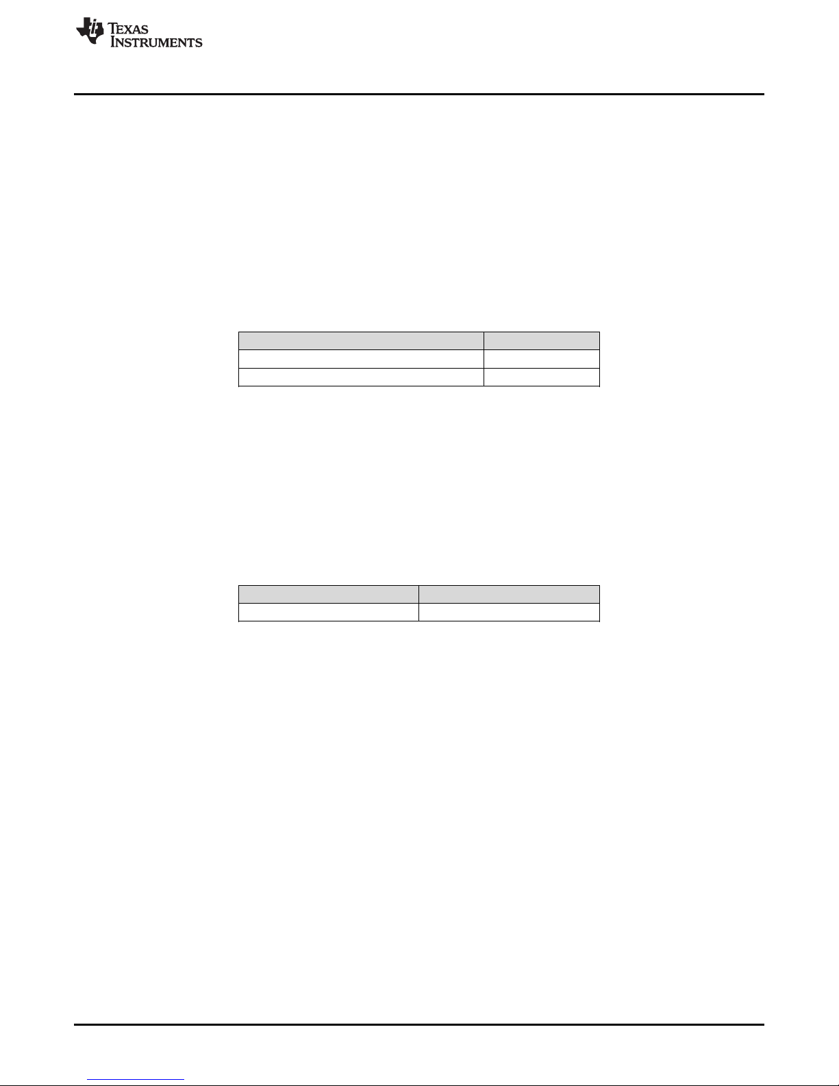
2 DACx0504EVM Hardware Setup
This section provides the overall system setup for the EVM. A PC runs software that communicates with
the USB2ANY platform, which generates the optional VIO power and digital signals used to communicate
with the EVM board. Test point connections are included on the EVM board for external power supplies.
Figure 1 displays the system setup for the DACx0504EVM.
www.ti.com
Figure 1. DACx0504EVM Hardware Setup
2.1 Theory of Operation for DACx0504 Hardware
A block diagram of the DACx0504EVM is displayed in Figure 2. The EVM board connects to the external
power supplies VDD and VIO through test points. The 16-pin header provides the four DAC outputs and
pullup or pulldown option for GAIN, RSTSEL, REFDIV, and LDAC inputs. The other two headers provide
options for external reference connection and VIO input from USB2ANY. The SPI signals can be provided
either via the USB2ANY header or test points. The USB2ANY controls the GAIN, RSTSEL, REFDIV and
LDAC pins by default.
Figure 2. DACx0504EVM Block Diagram
4
DACx0504 Evaluation Module
Copyright © 2017, Texas Instruments Incorporated
SLAU735A–July 2017–Revised October 2017
Submit Documentation Feedback
Page 5
www.ti.com
2.2 Signal Definition of USB2ANY
The DACx0504EVM provides a hardware connector (J1) that connects to the USB2ANY interface board,
which can supply VIO power and is responsible for providing the SPI commands sent from the PC GUI
software. Optionally, the VIO supply can be provided through an external supply, and all digital
communication lines can be accessed through their respective digital test points. This information is
provided in Table 3.
Table 3. J1 USB2ANY Signal Definition
Pin on J1 Signal Description
1 GPIO7 General purpose I/O
2 CS, GPIO6 CS | General purpose I/O
3 RXD, MISO SPI MISO
4 TXD, MOSI SPI MOSI
5 3.3V 3.3-V supply
6 GND Ground
7 GPIO3 General purpose I/O
8 SCLK, GPIO2 SPI SCLK
9 GPIO1 General purpose I/O
10 GPIO0 General purpose I/O
Table 4. J1 Digital Signal Test Points
DACx0504EVM Hardware Setup
Testpoints SPI Signal
TP1 SCLK
TP2 CS
TP3 SDI
TP4 SDO
SLAU735A–July 2017–Revised October 2017
Submit Documentation Feedback
Copyright © 2017, Texas Instruments Incorporated
DACx0504 Evaluation Module
5
Page 6
DACx0504EVM Software Setup
3 DACx0504EVM Software Setup
This section provides the procedure for EVM software installation.
3.1 Operating Systems for DACx0504EVM Software
The EVM software has been tested on the Microsoft®Windows®XP and Windows 7 operating systems
with the United States and European regional settings. The software should also be compatible with other
Windows operating systems.
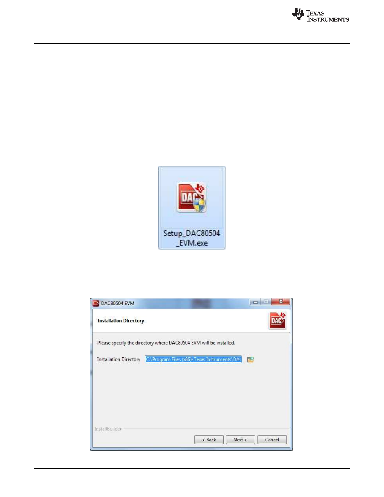
3.2 DACx0504EVM Software Installation
The software is available through the EVM product folder on the TI website. Once the software is
downloaded onto the PC, navigate to the DACx0504EVM folder, and run the Setup_DAC80504_EVM.exe
file, as shown in Figure 3. When the software is launched, an installation dialog will open, and prompt the
user to select an installation directory. If left unchanged, the software location defaults to C:\Program Files
(x86)\Texas Instruments\DAC80504 EVM as shown in Figure 4.
www.ti.com
Figure 3. Launching Software Setup
The software installation will automatically copy the required LabVIEW files and drivers to the local
machine. (Note: Please verify that the USB2ANY is not connected before the software installation, as this
may affect file or driver installation.)
6
DACx0504 Evaluation Module
Figure 4. DACx0504EVM Install Path
Copyright © 2017, Texas Instruments Incorporated
SLAU735A–July 2017–Revised October 2017
Submit Documentation Feedback
Page 7

www.ti.com
4 DACx0504EVM Hardware Overview
The subsequent sections provide detailed information on the EVM hardware, and jumper configuration
settings. Table 5 displays the default configurations of all jumper connections on the DACx0504EVM.
Connect the USB extender cable from the USB2ANY to the PC.
Table 5. Default Jumper Settings
Jumper Default Position Function
JP1 Shunt populated VIO supply from USB2ANY
4.1 Electrostatic Discharge Warning
Many of the components on the DACx0504EVM are susceptible to damage by electrostatic discharge
(ESD). Customers are advised to observe proper ESD handling precautions when unpacking and handling
the EVM, including the use of a grounded wrist strap at an approved ESD workstation.
4.2 Connecting the Hardware
To connect the USB2ANY to the EVM board, align and firmly connect the keyed ribbon connector to the
J1 connector. Verify the connection is snug, as loose connections may cause intermittent operation.
4.3 DACx0504EVM Power Configurations
The DACx0504EVM provides electrical connections to the device supply pins. The connectors and
optional configurations are shown in the Table 6.
DACx0504EVM Hardware Overview
controller
Table 6. DACx0504EVM Power Supply Configuration
ConnectorConnection Type Description
TP6 Test Point External VDD connection (2.7 V to 5.5 V)
TP8 Test Point External VIO connection
● JP1 populated (USB2ANY to power VIO)
● JP1 unpopulated (VIO powered through TP8)
VIO can be supplied by the USB2ANY by default. If a different source is required, it is possible to separate
the USB2ANY supply and VIO by removing the jumper from J1. An external supply can then connect to J5
to power VIO.
SLAU735A–July 2017–Revised October 2017
Submit Documentation Feedback
Copyright © 2017, Texas Instruments Incorporated
DACx0504 Evaluation Module
7
Page 8

DACx0504EVM Hardware Overview
4.4 DAC Signal Pins
The DACx0504EVM provides access to all DAC outputs through connection J2 as shown in Figure 5, and
listed in Table 7.
www.ti.com
Figure 5. DAC Output Connection Headers
Table 7. DACx0504EVM DAC Signal Connections
Name Connector Description
DACOUT0 J2-2 DAC output voltage
DACOUT1 J2-4 DAC output voltage
DACOUT2 J2-6 DAC output voltage
DACOUT3 J2-8 DAC output voltage
GAIN J2-10 DAC gain
RSTSEL J2-12 DAC reset select
REFDIV J2-14 DAC reference divider
LDAC J2-16 DAC Load DAC
4.5 SPI Communication Signals and Digital Inputs
The SPI signals are located on various test points and are described in Table 8, along with the digital input
signals of the DACx0504 device.
Table 8. SPI Signal Definition
Name Connector Description
SCLK TP1 Serial interface clock
MOSI TP3 Serial interface data input
MISO TP4 Serial interface data output
CS TP2 Active-low serial data enable
8
DACx0504 Evaluation Module
Copyright © 2017, Texas Instruments Incorporated
SLAU735A–July 2017–Revised October 2017
Submit Documentation Feedback
Page 9

www.ti.com
5 DACx0504EVM Software Overview
This section discusses how to use the DACx0504EVM software.
5.1 Starting the DACx0504EVM Software
Once the DACx0504EVM software is installed, a restart may be required by Windows. To launch the
software, locate the Texas Instruments folder in the All Programs menu and select the ‘DAC80504 EVM’
icon.
Figure 6. DACx0504EVM GUI Location
This section describes the features of the DACx0504EVM software. The software, as shown in Figure 7,
provides basic control of all the registers and functions to the DACx0504 device. If the USB2ANY is
correctly connected, the STATUS should display “HARDWARE CONNECTED”. If the USB2ANY is not
properly connected or not connected at all, the STATUS will display “DEMO”. If the GUI is not displaying
the “CONNECTED” status while the USB2ANY is connected, unplug and reconnect the USB2ANY and relaunch the GUI software.
DACx0504EVM Software Overview
Figure 7. DACx0504EVM GUI—Power On
5.2 DACx0504EVM Software Features
The DACx0504EVM incorporates interactive functions that help configure the DACx0504 device. These
functions are built into several GUI pages, as shown in Figure 8. The Page Selection menu allows the
user to switch between the pages; each page representing a feature of the software.
Figure 8. DACx0504EVM Software Page Selection
5.2.1 DACx0504EVM Low Level Configuration Page
The Register Map page of the DACx0504EVM allows the user to access low-level communication directly
with the registers of the DACx0504. Selecting a register on the Register Map list presents a description of
the values in that register as well as shows information on the address of the register’s, default value,
size, and current value. Values can be read and written to the registers by writing to the Value or bit field
of the GUI.
SLAU735A–July 2017–Revised October 2017
Submit Documentation Feedback
Copyright © 2017, Texas Instruments Incorporated
DACx0504 Evaluation Module
9
Page 10

DACx0504EVM Software Overview
www.ti.com
Figure 9. Low Level Configuration Page
The values of the register map can also be saved by pressing the Save Configuration button under the
File menu option. Additionally, the configuration files can be accessed through the Load Configuration
button.
Other options selectable by the user are the Update Mode, Write Selected (red box), Read Selected
(orange box), Write Modified (gray box), and Read All (yellow box) buttons. All buttons are displayed in
Figure 10.
Figure 10. Low Level Configuration Page Available Options
If Update Mode is selected to “Immediate”, all changes to register values will update immediately, while
“Deferred” allows the user to modify the value of a register without taking effect until the Write Selected, or
Write Modified button is pressed.
The Read Selected button allows individual register reads, while the Read All button reads the status of all
registers located in the register map.
10
DACx0504 Evaluation Module
Copyright © 2017, Texas Instruments Incorporated
SLAU735A–July 2017–Revised October 2017
Submit Documentation Feedback
Page 11

www.ti.com
5.2.2 DACx0504EVM High Level Configuration Page
The High Level Configuration page provides an interface to observe and control the different data
registers, modes, and configurations available for the DACx0504 device. This page is displayed in
Figure 11.
DACx0504EVM Software Overview
Internal Reference: By default, the internal reference is “ON”, which is displayed on the Internal
Reference button. The reference divider bit is also disabled at startup with a division denominator of “1”.
When pressed, the reference divider bit is set to “1”, which changes the denominator value to “2” – this
essentially halves the reference supply. This reference division provides flexibility when achieving specific
DAC output ranges; however, the reference and DAC output should be configured to ensure there is
sufficient headroom for VDD during normal operation. More information related to the reference divider is
shown in the DACx0504 data sheet.
Gain: The Gain buttons set the gain for the corresponding DAC outputs. At startup, the gain bit is cleared
to “0”, which sets the gain to 1. When this bit is set, the corresponding DAC has a gain of 2.
DAC Outputs: The DAC outputs can be enabled or disabled via the DAC ON button. The DAC outputs
are enabled by default. To write to the DACx Register, type the 16-bit hexadecimal value into the
corresponding DAC OUT Hex input field.
SLAU735A–July 2017–Revised October 2017
Submit Documentation Feedback
Figure 11. High Level Configuration Page
Copyright © 2017, Texas Instruments Incorporated
DACx0504 Evaluation Module
11
Page 12

DNC
1
VIN
2
TEMP
3
GND
4
TRIM/NR
5
VOUT
6
NC
7
DNC
8
U2
REF5050AID
+5VREF
VDD
GND
GNDGND
1µFC10.1µFC2100pF
C3
1µF
C4
1µF
C7
10µF
C5
GND
GND
1µF
C6
12
JP3
VDD
VIO
12
JP1 VIO
TP7 VREF
TP1 SCLK
TP2 \CS
TP3 SDI
TP4 SDO
TP5
TP6 VDD
GND
1 2
3 4
5 6
7 8
9 10
J1
RXD_MISO
USB_3p3
CS_GPIO6
TXD_MOSI
SCLK_GPIO2
USB2ANY Connection
GND
SCLK_GPIO2
CS_GPIO6
TXD_MOSI
RXD_MISO
USB_3p3
SCLK_GPIO2
CS_GPIO6
10.0k
R1
10.0k
R2
10.0kR310.0k
R4
12
JP2
12
JP4
12
JP512JP6
GND
TXD_MOSI
10.0k
R5
10.0k
R6
VIO
RXD_MISO
GND
U2A_GPIO7
U2A_GPIO3
U2A_GPIO1 U2A_GPIO0 U2A_GPIO7
U2A_GPIO3
U2A_GPIO1
U2A_GPIO0
1µFC80.1µF
C9
TP8
VIO
TP9
560pF
C10
GND
12
34
56
78
910
1112
1314
1516
J22.7V to 5.5V
1.7V to 5.5V
CS
12
GND
6
OUT0
2
OUT1
3
OUT2
4
OUT3
5
GAIN
8
RSTSEL
9
REFDIV
10
LDAC
11
REF
1
SCLK
13
SDI
14
SDO/ALARM
15
VDD
7
VIO
16
PAD
17
U1
DAC80504RTER
Copyright © 2017, Texas Instruments Incorporated
DACx0504EVM Documentation
www.ti.com
12
SLAU735A– July 2017–Revised October 2017
Submit Documentation Feedback
Copyright © 2017, Texas Instruments Incorporated
DACx0504 Evaluation Module
6 DACx0504EVM Documentation
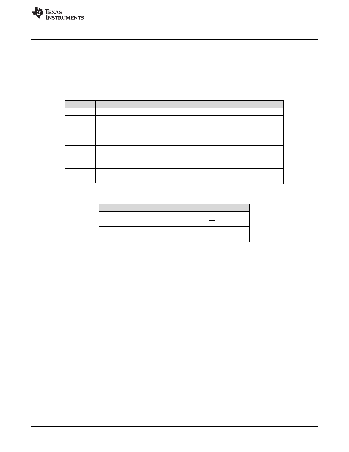
This section contains the complete bill of materials and schematic diagram for the DACx0504EVM.
6.1 DACx0504EVM Board Schematic
Figure 12 illustrates the DACx0504EVM board schematic.
Figure 12. DACx0504EVM Board Schematic
Page 13

www.ti.com
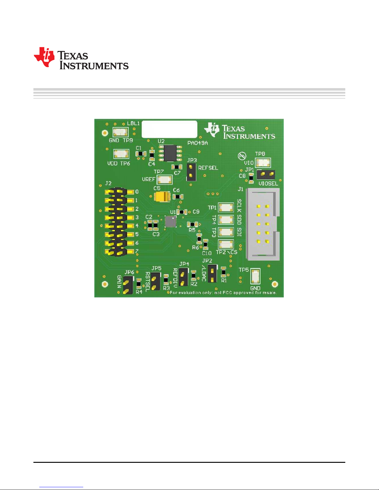
6.2 DACx0504EVM PCB Components Layout
Figure 13 shows the layout of the components for the DACx0504EVM board.
DACx0504EVM Documentation
Figure 13. DACx0504EVM PCB Components Layout
Figure 14. Top Layer
SLAU735A–July 2017–Revised October 2017
Submit Documentation Feedback
Copyright © 2017, Texas Instruments Incorporated
DACx0504 Evaluation Module
13
Page 14

DACx0504EVM Documentation
www.ti.com
Figure 15. Top Solder
14
DACx0504 Evaluation Module
Figure 16. Bottom Layer
Copyright © 2017, Texas Instruments Incorporated
SLAU735A–July 2017–Revised October 2017
Submit Documentation Feedback
Page 15

www.ti.com
DACx0504EVM Documentation
15
SLAU735A– July 2017–Revised October 2017
Submit Documentation Feedback
Copyright © 2017, Texas Instruments Incorporated
DACx0504 Evaluation Module
6.3 DACx0504EVM Bill of Materials
Table 9 lists the DACx0504 BOM.
(1)
Unless otherwise noted in the Alternate Part Number or Alternate Manufacturer columns, all parts may be substituted with equivalents.
Table 9. DACx0504EVM Bill of Materials
(1)
Designator Qty Value Description Package Reference Part Number Manufacturer Alternate Part
Number
Alternate
Manufacturer
!PCB 1 Printed Circuit Board PA049 Any - C1, C4, C6, C7, C8 5 1uF CAP, CERM, 1uF, 25V, +/-10%, X5R, 0603 0603 C1608X5R1E105K080AC TDK
C2, C9 2 0.1uF CAP, CERM, 0.1uF, 50V, +/-10%, X7R, 0603 0603 C0603C104K5RACTU Kemet
C3 1 100pF CAP, CERM, 100pF, 50V, +/-5%, C0G/NP0, 0603 0603 GRM1885C1H101JA01D Murata
C5 1 10uF CAP, TA, 10 µF, 16 V, +/- 10%, 0.8 ohm, SMD 3528-21 TPSB106K016R0800 AVX
C10 1 560pF CAP,CERM, 560 pF, 25 V, +/- 5%, C0G/NP0, 0603 0603 GRM1885C1E561JA01D Murata
H9, H10, H11, H12 4 Bumpon, Hemisphere, 0.44 X 0.20, Clear Transparent Bumpon SJ-5303 (CLEAR) 3M
J1 1 Header(Shrouded), 2.54mm, 5x2, Gold, TH Header, 2.54mm, 5x2, TH AWHW-10G-0202-T Assman WSW
J2 1 Header, 2.54mm, 8x2, Gold, SMT Header, 2.54mm, 8x2, SMT TSM-108-01-L-DV Samtec
JP1, JP2, JP3, JP4,
JP5, JP6
6 Header, TH, 100mil, 2x1, Gold plated, 230 mil above insulator 2x1 Header TSW-102-07-G-S Samtec
LBL1 1 Thermal Transfer Printable Labels, 0.650" W x 0.200" H - 10,000
per roll
PCB Label 0.650 x 0.200 inch THT-14-423-10 Brady
R1, R2, R3, R4, R5,R66 10.0k RES, 10.0k ohm, 1%, 0.1W, 0603 0603 RC0603FR-0710KP Yageo America
SH-J1, SH-J2, SH-J3,
SH-J4, SH-J5, SH-J6,
SH-J7, SH-J8, SH-J9,
SH-J10
10 Shunt,100mil, Gold plated, Black Shunt 2 pos. 100 mil 881545-2 TEConnectivity
TP1, TP2, TP3, TP4,
TP5, TP6, TP7, TP8,
TP9
9 Test Point, Miniature, SMT Test Point, Miniature, SMT 5019 Keystone
U1 1 Quad, True 16-/14-/12-Bit, SPI Voltage Output DAC with
Precision Internal Reference, RTE0016D (WQFN-16)
RTE0016D DAC80504RTER,
DAC70504RTER,
DAC60504RTER
Texas Instruments DAC80504RTET,
DAC70504RTET,
DAC60504RTET
Texas
Instruments
U2 1 Low-Noise, Very Low Drift, Precision VOLTAGE REFERENCE,
D0008A
D0008A REF5050AID Texas Instruments
FID1, FID2, FID3 0 Fiducial mark. There is nothing to buy or mount. Fiducial N/A N/A
Page 16

Revision History
www.ti.com
Revision History
NOTE: Page numbers for previous revisions may differ from page numbers in the current version.
Changes from Original (July 2017) to A Revision ........................................................................................................... Page
• Changed all instances of DAC80504 to DACx0504.................................................................................. 1
• Changed the DAC from eight-channel to four-channel............................................................................... 3
• Changed part number from RC0603FR-0710KL to RC0603FR-0710KP in Table 9: DACx0504EVM Bill of Materials.... 15
• Added part numbers DAC70504RTER and DAC60504RTER to designator U1 in Table 9: DACx0504EVM Bill of
Materials .................................................................................................................................. 15
• Added alternate part numbers DAC70504RTET and DAC60504RTET to designator U1 in Table 9: DACx0504EVM Bill of
Materials .................................................................................................................................. 15
16
Revision History
Copyright © 2017, Texas Instruments Incorporated
SLAU735A–July 2017–Revised October 2017
Submit Documentation Feedback
Page 17

IMPORTANT NOTICE FOR TI DESIGN INFORMATION AND RESOURCES
Texas Instruments Incorporated (‘TI”) technical, application or other design advice, services or information, including, but not limited to,
reference designs and materials relating to evaluation modules, (collectively, “TI Resources”) are intended to assist designers who are
developing applications that incorporate TI products; by downloading, accessing or using any particular TI Resource in any way, you
(individually or, if you are acting on behalf of a company, your company) agree to use it solely for this purpose and subject to the terms of
this Notice.
TI’s provision of TI Resources does not expand or otherwise alter TI’s applicable published warranties or warranty disclaimers for TI
products, and no additional obligations or liabilities arise from TI providing such TI Resources. TI reserves the right to make corrections,
enhancements, improvements and other changes to its TI Resources.
You understand and agree that you remain responsible for using your independent analysis, evaluation and judgment in designing your
applications and that you have full and exclusive responsibility to assure the safety of your applications and compliance of your applications
(and of all TI products used in or for your applications) with all applicable regulations, laws and other applicable requirements. You
represent that, with respect to your applications, you have all the necessary expertise to create and implement safeguards that (1)
anticipate dangerous consequences of failures, (2) monitor failures and their consequences, and (3) lessen the likelihood of failures that
might cause harm and take appropriate actions. You agree that prior to using or distributing any applications that include TI products, you
will thoroughly test such applications and the functionality of such TI products as used in such applications. TI has not conducted any
testing other than that specifically described in the published documentation for a particular TI Resource.
You are authorized to use, copy and modify any individual TI Resource only in connection with the development of applications that include
the TI product(s) identified in such TI Resource. NO OTHER LICENSE, EXPRESS OR IMPLIED, BY ESTOPPEL OR OTHERWISE TO
ANY OTHER TI INTELLECTUAL PROPERTY RIGHT, AND NO LICENSE TO ANY TECHNOLOGY OR INTELLECTUAL PROPERTY
RIGHT OF TI OR ANY THIRD PARTY IS GRANTED HEREIN, including but not limited to any patent right, copyright, mask work right, or
other intellectual property right relating to any combination, machine, or process in which TI products or services are used. Information
regarding or referencing third-party products or services does not constitute a license to use such products or services, or a warranty or
endorsement thereof. Use of TI Resources may require a license from a third party under the patents or other intellectual property of the
third party, or a license from TI under the patents or other intellectual property of TI.
TI RESOURCES ARE PROVIDED “AS IS” AND WITH ALL FAULTS. TI DISCLAIMS ALL OTHER WARRANTIES OR
REPRESENTATIONS, EXPRESS OR IMPLIED, REGARDING TI RESOURCES OR USE THEREOF, INCLUDING BUT NOT LIMITED TO
ACCURACY OR COMPLETENESS, TITLE, ANY EPIDEMIC FAILURE WARRANTY AND ANY IMPLIED WARRANTIES OF
MERCHANTABILITY, FITNESS FOR A PARTICULAR PURPOSE, AND NON-INFRINGEMENT OF ANY THIRD PARTY INTELLECTUAL
PROPERTY RIGHTS.
TI SHALL NOT BE LIABLE FOR AND SHALL NOT DEFEND OR INDEMNIFY YOU AGAINST ANY CLAIM, INCLUDING BUT NOT
LIMITED TO ANY INFRINGEMENT CLAIM THAT RELATES TO OR IS BASED ON ANY COMBINATION OF PRODUCTS EVEN IF
DESCRIBED IN TI RESOURCES OR OTHERWISE. IN NO EVENT SHALL TI BE LIABLE FOR ANY ACTUAL, DIRECT, SPECIAL,
COLLATERAL, INDIRECT, PUNITIVE, INCIDENTAL, CONSEQUENTIAL OR EXEMPLARY DAMAGES IN CONNECTION WITH OR
ARISING OUT OF TI RESOURCES OR USE THEREOF, AND REGARDLESS OF WHETHER TI HAS BEEN ADVISED OF THE
POSSIBILITY OF SUCH DAMAGES.
You agree to fully indemnify TI and its representatives against any damages, costs, losses, and/or liabilities arising out of your noncompliance with the terms and provisions of this Notice.
This Notice applies to TI Resources. Additional terms apply to the use and purchase of certain types of materials, TI products and services.
These include; without limitation, TI’s standard terms for semiconductor products http://www.ti.com/sc/docs/stdterms.htm), evaluation
modules, and samples (http://www.ti.com/sc/docs/sampterms.htm).
Mailing Address: Texas Instruments, Post Office Box 655303, Dallas, Texas 75265
Copyright © 2017, Texas Instruments Incorporated
 Loading...