

Page 1

User's Guide
SLAU726–August 2017
DAC90x Evaluation Module
This user's guide describes the function and use of the DAC90x evaluation module (EVM). Included in this
document are a quick-start guide, instructions for optimizing evaluation results, jumper and connector
descriptions, software description, and alternate hardware configurations.
Contents
1 Overview...................................................................................................................... 2
1.1 Required Hardware................................................................................................. 2
1.2 Required Software.................................................................................................. 3
1.3 Evaluation Board Feature Identification Summary ............................................................. 3
1.4 References .......................................................................................................... 3
2 Quick-Start Guide............................................................................................................ 4
2.1 Software Installation................................................................................................ 4
2.2 Hardware Setup Procedure ....................................................................................... 5
2.3 Software Setup Procedure......................................................................................... 6
2.4 Quick-Start Troubleshooting....................................................................................... 8
3 Alternate Hardware Configurations........................................................................................ 9
3.1 Control Modes....................................................................................................... 9
3.2 External Clock Generation ....................................................................................... 10
3.3 Analog Output Circuits............................................................................................ 10
Appendix A Jumper and Connector Descriptions............................................................................ 12
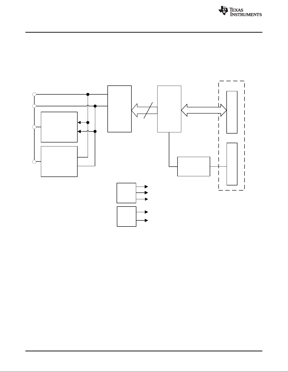
1 DAC90xEVM Block Diagram............................................................................................... 2
2 EVM Feature Locations..................................................................................................... 3
3 Quick-Start Test Setup...................................................................................................... 5
4 Power Supply Connections................................................................................................. 6
5 HSDC Pro GUI Main Panel................................................................................................. 7
6 Reconfiguration Hardware Location....................................................................................... 9
7 External Clock Signal ...................................................................................................... 10
1 Configuration Files........................................................................................................... 7
2 Troubleshooting Tips ........................................................................................................ 8
3 Jumper Descriptions and Default Settings.............................................................................. 12
4 Connector Descriptions.................................................................................................... 12
5 J1 Parallel Data Connector ............................................................................................... 13
6 J4 and J2 Power Connectors............................................................................................. 13
Trademarks
Microsoft, Windows are registered trademarks of Microsoft Corporation.
All other trademarks are the property of their respective owners.
List of Figures
List of Tables
SLAU726–August 2017
Submit Documentation Feedback
Copyright © 2017, Texas Instruments Incorporated
DAC90x Evaluation Module
1
Page 2
*Unpopulated components
TSW1400EVM Interface
DAC Buffers
Control
Interface
*
14
J6
J7
J8
J9
*
*
J4
J2
5 VA
AGND
-5 VA
3.3 V (DVDD)
DGND
DP
Amplifier
Interface
Transformer
Interface
D[0-15]
J1
J3
*
Copyright © 2017, Texas Instruments Incorporated
Overview
1 Overview
The DAC90xEVM is an evaluation module (EVM) designed to evaluate the DAC90x. The EVM provides
simple and minimal external components to minimize system cost and power consumption. The
DAC90xEVM is designed to work seamlessly with the TSW1400EVM, data capture and pattern generator
module. The TSW1400EVM is programed through TI's High-Speed Data Converter Pro Graphic User
Interface (HSDC Pro GUI) software tool for high-speed data converter evaluation.
www.ti.com
1.1 Required Hardware
The following equipment is included in the EVM evaluation kit:
• DAC90xEVM
The following list of equipment are items that are not included in the EVM evaluation kit but are items
required for evaluation of this product in order to achieve the best performance:
• TSW1400EVM Data Capture Board, +5 V DC cable connector and mini-USB cable
• Computer running Microsoft®Windows®8, Windows 7, or Windows XP
• One dual-channel pulse generator.
– Examples: Keysight 81160A, 81134A, 8133a, or similar.
• Triple-output DC power supply. Recommendations:
– DC Power Supply, Output 1: 30 W, 6 V, 5 A. Output 2: 25 W, 25 V, 1 A, Output 3: 25 W, –25 V, 1
A.
– Examples: Keysight E3631A or equivalent
2
DAC90x Evaluation Module
Figure 1. DAC90xEVM Block Diagram
Copyright © 2017, Texas Instruments Incorporated
Submit Documentation Feedback
SLAU726–August 2017
Page 3
www.ti.com
• Signal path cables, SMA or BNC with BNC-to-SMA adapters
• One of the following (depending on the requirements of the user)
– Spectrum Analyzer. Example: Agilent E4440A
– Oscilloscope: Example: Agilent DSO3052T
1.2 Required Software
The following software is required to operate the TSW1400EVM and is available online. See References,
Section 1.4 for links.
• High-Speed Data Converter Pro software version 4.7
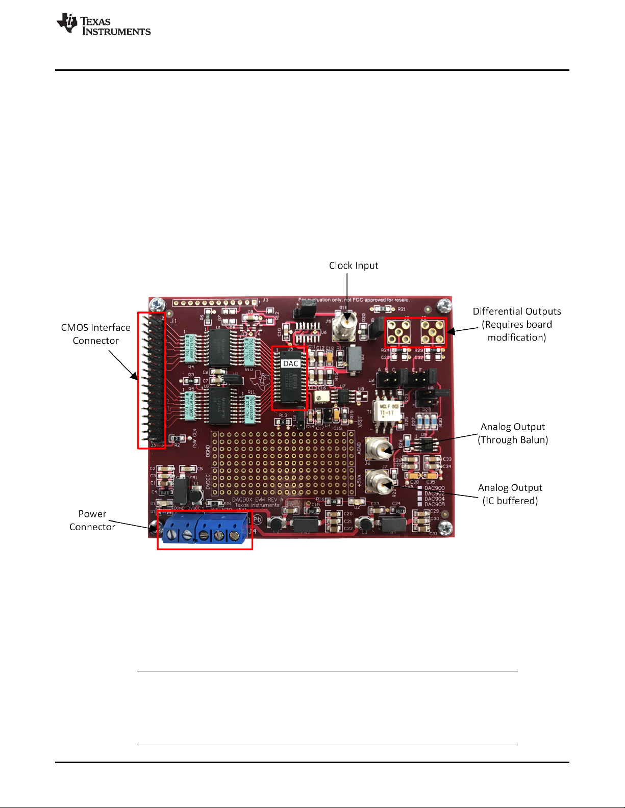
1.3 Evaluation Board Feature Identification Summary
The EVM features are labeled in Figure 2.
Overview
1.4 References
• DAC90x data sheet (SBAS093), available at www.ti.com/product/DAC900
• TSW1400EVM User’s Guide (SLWU079), available at www.ti.com/tool/TSW1400EVM
• High-Speed Data Converter Pro software (SLWC107) and User's Guide (SLWU087), available at
www.ti.com/tool/dataconverterpro-sw
NOTE: Schematics, layout, and BOM are available on each EVM tool page on www.ti.com:
• DAC900EVM
• DAC902EVM
• DAC904EVM
• DAC908EVM
SLAU726–August 2017
Submit Documentation Feedback
Figure 2. EVM Feature Locations
Copyright © 2017, Texas Instruments Incorporated
DAC90x Evaluation Module
3
Page 4

Quick-Start Guide
2 Quick-Start Guide
This section guides the user through the EVM test procedure to obtain a valid data capture from the
DAC90xEVM using the TSW1400EVM capture card. This should be the starting point for all evaluations.
2.1 Software Installation
The proper software must be installed before beginning evaluation. See Section 1.2 for a list of the
required software. The References section of this document contains links to find the software on the TI
website.
Important: The software must be installed before connecting the DAC90xEVM and TSW1400EVM to the
computer for the first time.
2.1.1 High-Speed Data Converter Pro GUI Installation
The High-Speed Data Converter Pro (HSDC Pro) is used to control the TSW1400EVM and analyze the
captured data. See High Speed Data Converter Pro GUI for more information.
1. Download HSDC Pro from the TI website. The References section of this document contains the link to
find the software on the TI website.
2. Extract the files from the zip file.
3. Run setup.exe and follow the installation prompts.
www.ti.com
4
DAC90x Evaluation Module
Copyright © 2017, Texas Instruments Incorporated
Submit Documentation Feedback
SLAU726–August 2017
Page 5
PC Running
HSDC Pro
5 VDC
Spectrum Analyzer
Dual-Channel
Pulse Generator
Triple-Output DC
Power Supply
Mini USB
www.ti.com
2.2 Hardware Setup Procedure
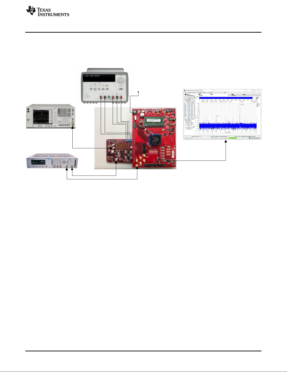
A typical test setup using the DAC90xEVM and TSW1400EVM is shown in Figure 3. This is the test setup
used for the quick-start procedure. The rest of this section describes the hardware setup steps.
Quick-Start Guide
2.2.1 TSW1400EVM Setup
Figure 3. Quick-Start Test Setup
Set up the TSW1400EVM with the following steps:
1. Connect the DAC90xEVM to the TSW1400EVM by connecting pin 1 of the CMOS_INTERFACE (J1) to
pin 1 of the DAC90xEVM output data (J1).
2. Connect the power cable to connector J12 (+5 V IN) to the TSW1400EVM.
3. Connect the mini-USB cable to the USB connector (J5).
4. Turn on the power supply. Flip the power switch (SW7) to the ON position. The board should draw
around 0.5 A after power up. This will increase to around 1.7 A when loaded with firmware.
SLAU726–August 2017
Submit Documentation Feedback
Copyright © 2017, Texas Instruments Incorporated
DAC90x Evaluation Module
5
Page 6
Quick-Start Guide
2.2.2 DAC90xEVM Setup
Continue the hardware setup of the DAC90xEVM using the following:
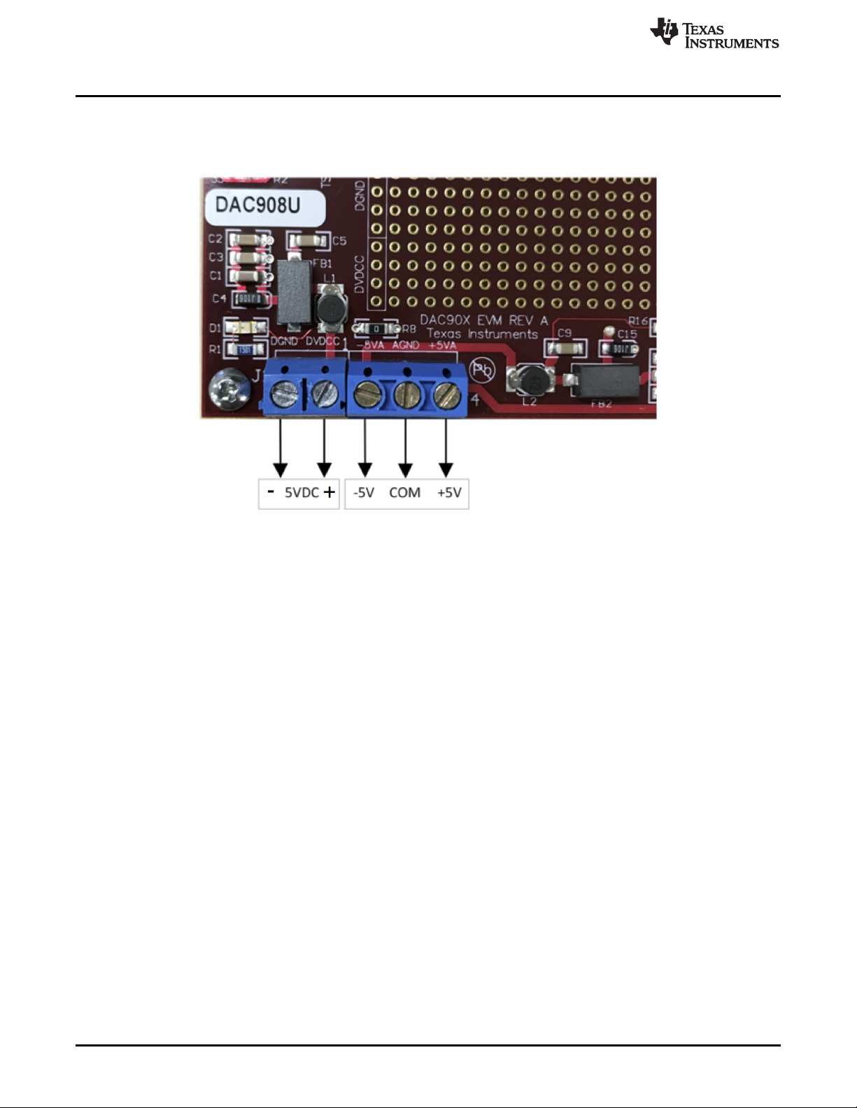
1. Connect the power supply cables to the EVM. refer to Figure 2 and Table 6 for proper connections.
www.ti.com
Figure 4. Power Supply Connections
2. Connect the SMA connector from the pulse generator to the EXT Clock input (J5).
3. Turn on the power supply.
4. Connect an SMA cable from the output of the DAC90xEVM (J6) to the input of the spectrum analyzer.
2.3 Software Setup Procedure
The software can be opened and configured once the hardware is properly setup.
2.3.1 HSDC Pro GUI Configuration
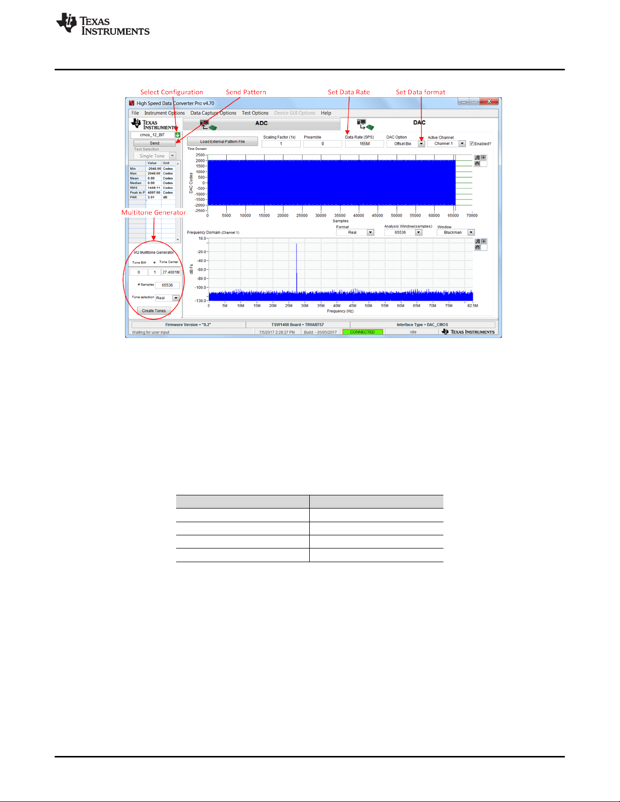
1. Open High Speed Data Converter Pro by going to Start Menu → All Programs → Texas Instruments →
High Speed Data Converter Pro. The GUI main page looks as shown in Figure 5.
6
DAC90x Evaluation Module
Copyright © 2017, Texas Instruments Incorporated
Submit Documentation Feedback
SLAU726–August 2017
Page 7
www.ti.com
Quick-Start Guide
Figure 5. HSDC Pro GUI Main Panel
2. When prompted to select the capture board, select the TSW1400. If multiple TSW1400EVMs are
connected, choose the serial number that corresponds to the serial number on the TSW1400EVM
connected to the DAC90x and click OK. This popup can be accessed through the Instrument Options
menu.
3. If no firmware is currently loaded, there is a message indicating this. Click OK.
4. Verify the DAC tab at the top of the GUI is selected.
5. Use the Select DAC drop-down menu at the top left corner to select the correct configuration file for
the DAC90x variant being used, see Table 1.
Table 1. Configuration Files
DAC90xEVM Variant Configuration File
DAC900 CMOS_10_Bit
DAC902 CMOS_12_Bit
DAC904 CMOS_14_Bit
DAC908 CMOS_8_Bit
6. When prompted to update the firmware for the DAC, click Yes and wait for the firmware to download to
the TSW1400. This takes approximately 10 seconds.
7. Enter “150M” into the "Data Rate (SPS)" field at the upper portion of the DAC tab, and ensure that
"offset Bin" is selected for "DAC Option".
8. In the lower left corner of the HSDC Pro window, enter the following parameters into the I/Q Multitone
generator:
• ToneBW = 0
• # = 1
• Tone Center = 27.4
9. Click the Create Tones button
10. The result should be now visible on the oscilloscope or spectrum analyzer. If performance is not
meeting data sheet specifications, it may be necessary to provide a delay on the clock signal to the
DAC in order to meet setup and hold time requirements. If no output is seen, then see Quick Start
Troubleshooting.
SLAU726–August 2017
Submit Documentation Feedback
Copyright © 2017, Texas Instruments Incorporated
DAC90x Evaluation Module
7
Page 8

Quick-Start Guide
2.4 Quick-Start Troubleshooting
Use Table 2 to assist with problems that may have occurred during the quick-start procedure.
Issue Troubleshooting Tips
General problems Verify the test setup shown in Section 2 and repeat the setup procedure as described in
TSW1400 LEDs are not correct:
D2 – D9 OFF
HSDC Pro software is not
capturing good data or analysis
results are incorrect.
HSDC Pro software gives a timeout error when capturing data
Sub-optimal measured
performance
www.ti.com
Table 2. Troubleshooting Tips
this document.
Check power supplies to the EVMs. Verify that the power switches are in the ON position
and supplies are drawing the appropriate current.
Check signal and clock connections to the EVM.
Check that all boards are properly connected together.
Try power-cycling the external power supply to the EVMs.
Verify the settings of the configuration switches on the TSW1400EVM.
Verify that the EVM configuration GUI is communicating with the USB and that the
configuration procedure has been followed.
Try capturing data in HSDC Pro to force an LED status update.
Verify that the TSW1400EVM is properly connected to the PC with a mini-USB cable and
that the board serial number is properly identified by the HSDC Pro software.
Check that the proper DAC device is selected, and the proper configuration file is being
used.
Check that the analysis parameters are properly configured.
Restart HSDC Pro and reload the firmware.
Verify that the data rate is correct in the HSDC Pro software.
Adjust the delay time of DAC clock.
Measure test points to verify operating voltage ranges.
Verify jumper configurations are in default locations.
Verify that filters are used in the clock and input signal paths and that low-noise signal
sources are used.
8
DAC90x Evaluation Module
Copyright © 2017, Texas Instruments Incorporated
Submit Documentation Feedback
SLAU726–August 2017
Page 9
www.ti.com
3 Alternate Hardware Configurations
This section describes alternate hardware configurations in order to achieve better results or to more
closely mimic the system configuration.
Alternate Hardware Configurations
3.1 Control Modes
The INT/EXT, REFinand FSA pins of the DAC904, DAC902, DAC900, and DAC908 control various DAC
features and functions. This section describes the function of these pins.
3.1.1 FSA Input Pin
For an output current of 20 mA, the potentiometer R14 value is typically set to 2 kΩ. Owing to the fact that
the maximum full-scale current is 20 mA when IOUT1 and IOUT2 are terminated into 50-Ω load resistors,
the voltage at J8 and J9 is 1 V.
3.1.2 INT/EXT Pin
The internal 1.2-V Vref is selected when the INT/EXT pin is grounded (W3 pins 2 and 3 shorted). When
the INT/EXT pin is tied to 5 V ( W3 pins 2 and 3 shorted) and the W4 jumper is in place, the external 1.2-V
Vref is selected.
SLAU726–August 2017
Submit Documentation Feedback
Figure 6. Reconfiguration Hardware Location
Copyright © 2017, Texas Instruments Incorporated
DAC90x Evaluation Module
9
Page 10

W2
1
2
3
DAC Clock
CLKOUT
DAC
J5
J1-33
Alternate Hardware Configurations
3.1.3 REFinPin
An external reference voltage is provided via the REFininput pin. U7 or U8 is used to generate the
external reference voltage. Jumper W4 is for selecting the external reference voltage.
3.2 External Clock Generation
When connected to an AVDD supply of 5 V and DVDD supply of 5 V, the maximum operating speed of
the DAC90x is 200 MHz. When the DVDD supply is 3.3 V, the maximum clock speed is 165 MHz. The
clock signal comes from either the DSP CLKOUT signal or from an external source via J5. The
DAC90xEVM requires an external clock source when used with the TSW1400EVM.
www.ti.com
Figure 7. External Clock Signal
3.3 Analog Output Circuits
The analog signal output of the DAC90x can be configured to drive a resistive load, a transformer, an
operational amplifier, or other output configuration, as long as the limitations set by the output voltage
compliance and full-scale range are not exceeded.
3.3.1 Transformer-Coupled Output
The optimum dynamic performance of the DAC90x is achieved with the outputs used differentially. The
DAC90xEVM is configured to operate with transformer output coupling by default. The 1:1 RF transformer
is used for impedance matching, dc isolation, and interfacing between the differential outputs of the DAC
and an external single-ended device. The resistors R23, R24, and R29 are used to form a network that
reflects 50 Ω across the primary circuit (J6).
A spectrum analyzer with 50-Ω input impedance is normally used to measure the performance of the DAC.
A 50-Ω coaxial cable is used to connect J6 output to the 50-Ω input of the spectrum analyzer. The
spectrum analyzer impedance is in parallel to the transformer 50-Ω reflected impedance across J6.
Therefore, the voltage at the input of the spectrum analyzer is ½ J6. If a larger voltage is required, use a
1:2 step up voltage ratio transformer to produce twice the voltage at J6. In addition set R23 to 200 Ω and
remove R24 and R29. R14 may require some adjustments.
3.3.2 Direct Output
Direct output configuration allows the user to connect the outputs of the DAC90x directly to external
circuitry. This configuration requires that J8 and J9 be installed by the user. A 1-V output will appear at J8
and J9 when IOUT1 and IOUT2 are terminated into 50-Ω external resistor loads (output taken from J8 and
J9 and W6 and W7 open).
3.3.3 Operational Amplifier Output
In addition to the transformer-coupled output configuration, the DAC90xEVM offers three more
configurations which use the THS3001 operational amplifier. The THS3001 can be configured as a
difference amplifier, an inverting amplifier, and a non-inverting amplifier.
10
DAC90x Evaluation Module
Copyright © 2017, Texas Instruments Incorporated
Submit Documentation Feedback
SLAU726–August 2017
Page 11

www.ti.com
3.3.3.1 Difference Amplifier Configuration
The THS3001 operates as a differential amplifier when: W9 is left opened, W8 pins 1 and 2 are connected
together, W6 position A is connected to IOUT1, and W7 position D is connected to IOUT2.
3.3.3.2 Inverting Amplifier Configuration
The THS3001 operates as an inverting amplifier under the following conditions: W9 is connected, R27 is
set to 0 Ω, W8 pins 1 and 2 are connected together, and the input is from either W6 position B or W7
position D. If the input is via W6 position B, the output at J7 is –1.2 V. If the input is via W7 position D, the
output will be –1.2 V.
3.3.3.3 Non-Inverting Amplifier Configuration
The THS3001 operates as a non-inverting amplifier when: W9 is opened, W8 pins 2 and 3 are connected
together, and the input is from either W6 position A or W7 position E. If the input is via W6 position A, the
output voltage is 2 V. If the input is taken via W7 position E, the output voltage at J7 is 2 V.
Alternate Hardware Configurations
SLAU726–August 2017
Submit Documentation Feedback
Copyright © 2017, Texas Instruments Incorporated
DAC90x Evaluation Module
11
Page 12

A.1 Jumper Descriptions
The EVM jumpers are shown in Table 3 as well as the default settings for the jumpers. Use this table to
reset the EVM in the default configuration, in case of issues.
Jumper Description Default Setting
W1 OE input for the SN74LVT245B buffers Shunt pins 1-2
W2 Selects CLKOUT signal from the DSP or clock input from signal gen. Shunt pins 2-3
W3 Selects external or internal Vref. Shunt pins 1-2
W4 Supplies external Vref to the DAC Open
W5 No function N/A
W6 Selects IOUT1 or IOUT2 output from DAC to amplifier or transformer Position C
W7 Selects IOUT1 or IOUT2 output from DAC to amplifier or transformer Position F
W8 Configures the op amp for either differential input, noninverting or
inverting mode
W9 Configures the op amp for inverting, noninverting or differential mode Open
Appendix A
SLAU726–August 2017
Jumper and Connector Descriptions
Table 3. Jumper Descriptions and Default Settings
Shunt pins 2-3
A.1.1 Connector Descriptions
The EVM connectors and their function are described in Table 4.
Reference Designator Function
J1 Data bits 0 through 13 and CLKOUT input
J2, J4 Supplies power to the EVM
J3 Input control signals used to create EVM chip select
J5 Input for a clock signal source
J6, J7, J8, J9 DAC output signal
Table 4. Connector Descriptions
12
Jumper and Connector Descriptions
Copyright © 2017, Texas Instruments Incorporated
Submit Documentation Feedback
SLAU726–August 2017
Page 13

www.ti.com
A.1.2 CMOS Data Connector Pinout
The J1 parallel data connector pins and functions are listed in Table 5.
Table 5. J1 Parallel Data Connector
Pin Number Function Pin Number Function
1 DSP_15 (MSB) 2 Ground (digital)
3 DSP_14 4 Ground (digital)
5 DSP_13 6 Ground (digital)
7 DSP_12 8 Ground (digital)
9 DSP_11 10 Ground (digital)
11 DSP_10 12 Ground (digital)
13 DSP_09 14 Ground (digital)
15 DSP_08 16 Ground (digital)
17 DSP_07 18 Ground (digital)
19 DSP_06 20 Ground (digital)
21 DSP_05 22 Ground (digital)
23 DSP_04 24 Ground (digital)
25 DSP_03 26 Ground (digital)
27 DSP_02 28 Ground (digital)
29 DSP_01 30 Ground (digital)
31 DSP_00 (LSB) 32 Ground (digital)
33 CLKOUT 34 Ground (digital)
Jumper Descriptions
A.1.3 Power Connectors
The J4 and J2 power connector pins and their functions are listed in Table 6.
Table 6. J4 and J2 Power Connectors
Pin Number Function
J2–1 Digital power 3 V–5 V
J2–2 DGND
J4–1 Analog power +5 V
J4–2 AGND
J4–3 Analog power –5 V
SLAU726–August 2017
Submit Documentation Feedback
Copyright © 2017, Texas Instruments Incorporated
Jumper and Connector Descriptions
13
Page 14

STANDARD TERMS FOR EVALUATION MODULES
1. Delivery: TI delivers TI evaluation boards, kits, or modules, including any accompanying demonstration software, components, and/or
documentation which may be provided together or separately (collectively, an “EVM” or “EVMs”) to the User (“User”) in accordance
with the terms set forth herein. User's acceptance of the EVM is expressly subject to the following terms.
1.1 EVMs are intended solely for product or software developers for use in a research and development setting to facilitate feasibility
evaluation, experimentation, or scientific analysis of TI semiconductors products. EVMs have no direct function and are not
finished products. EVMs shall not be directly or indirectly assembled as a part or subassembly in any finished product. For
clarification, any software or software tools provided with the EVM (“Software”) shall not be subject to the terms and conditions
set forth herein but rather shall be subject to the applicable terms that accompany such Software
1.2 EVMs are not intended for consumer or household use. EVMs may not be sold, sublicensed, leased, rented, loaned, assigned,
or otherwise distributed for commercial purposes by Users, in whole or in part, or used in any finished product or production
system.
2 Limited Warranty and Related Remedies/Disclaimers:
2.1 These terms do not apply to Software. The warranty, if any, for Software is covered in the applicable Software License
Agreement.
2.2 TI warrants that the TI EVM will conform to TI's published specifications for ninety (90) days after the date TI delivers such EVM
to User. Notwithstanding the foregoing, TI shall not be liable for a nonconforming EVM if (a) the nonconformity was caused by
neglect, misuse or mistreatment by an entity other than TI, including improper installation or testing, or for any EVMs that have
been altered or modified in any way by an entity other than TI, (b) the nonconformity resulted from User's design, specifications
or instructions for such EVMs or improper system design, or (c) User has not paid on time. Testing and other quality control
techniques are used to the extent TI deems necessary. TI does not test all parameters of each EVM.
User's claims against TI under this Section 2 are void if User fails to notify TI of any apparent defects in the EVMs within ten (10)
business days after delivery, or of any hidden defects with ten (10) business days after the defect has been detected.
2.3 TI's sole liability shall be at its option to repair or replace EVMs that fail to conform to the warranty set forth above, or credit
User's account for such EVM. TI's liability under this warranty shall be limited to EVMs that are returned during the warranty
period to the address designated by TI and that are determined by TI not to conform to such warranty. If TI elects to repair or
replace such EVM, TI shall have a reasonable time to repair such EVM or provide replacements. Repaired EVMs shall be
warranted for the remainder of the original warranty period. Replaced EVMs shall be warranted for a new full ninety (90) day
warranty period.
3 Regulatory Notices:
3.1 United States
3.1.1 Notice applicable to EVMs not FCC-Approved:
FCC NOTICE: This kit is designed to allow product developers to evaluate electronic components, circuitry, or software
associated with the kit to determine whether to incorporate such items in a finished product and software developers to write
software applications for use with the end product. This kit is not a finished product and when assembled may not be resold or
otherwise marketed unless all required FCC equipment authorizations are first obtained. Operation is subject to the condition
that this product not cause harmful interference to licensed radio stations and that this product accept harmful interference.
Unless the assembled kit is designed to operate under part 15, part 18 or part 95 of this chapter, the operator of the kit must
operate under the authority of an FCC license holder or must secure an experimental authorization under part 5 of this chapter.
3.1.2 For EVMs annotated as FCC – FEDERAL COMMUNICATIONS COMMISSION Part 15 Compliant:
CAUTION
This device complies with part 15 of the FCC Rules. Operation is subject to the following two conditions: (1) This device may not
cause harmful interference, and (2) this device must accept any interference received, including interference that may cause
undesired operation.
Changes or modifications not expressly approved by the party responsible for compliance could void the user's authority to
operate the equipment.
FCC Interference Statement for Class A EVM devices
NOTE: This equipment has been tested and found to comply with the limits for a Class A digital device, pursuant to part 15 of
the FCC Rules. These limits are designed to provide reasonable protection against harmful interference when the equipment is
operated in a commercial environment. This equipment generates, uses, and can radiate radio frequency energy and, if not
installed and used in accordance with the instruction manual, may cause harmful interference to radio communications.
Operation of this equipment in a residential area is likely to cause harmful interference in which case the user will be required to
correct the interference at his own expense.
Page 15

FCC Interference Statement for Class B EVM devices
NOTE: This equipment has been tested and found to comply with the limits for a Class B digital device, pursuant to part 15 of
the FCC Rules. These limits are designed to provide reasonable protection against harmful interference in a residential
installation. This equipment generates, uses and can radiate radio frequency energy and, if not installed and used in accordance
with the instructions, may cause harmful interference to radio communications. However, there is no guarantee that interference
will not occur in a particular installation. If this equipment does cause harmful interference to radio or television reception, which
can be determined by turning the equipment off and on, the user is encouraged to try to correct the interference by one or more
of the following measures:
• Reorient or relocate the receiving antenna.
• Increase the separation between the equipment and receiver.
• Connect the equipment into an outlet on a circuit different from that to which the receiver is connected.
• Consult the dealer or an experienced radio/TV technician for help.
3.2 Canada
3.2.1 For EVMs issued with an Industry Canada Certificate of Conformance to RSS-210 or RSS-247
Concerning EVMs Including Radio Transmitters:
This device complies with Industry Canada license-exempt RSSs. Operation is subject to the following two conditions:
(1) this device may not cause interference, and (2) this device must accept any interference, including interference that may
cause undesired operation of the device.
Concernant les EVMs avec appareils radio:
Le présent appareil est conforme aux CNR d'Industrie Canada applicables aux appareils radio exempts de licence. L'exploitation
est autorisée aux deux conditions suivantes: (1) l'appareil ne doit pas produire de brouillage, et (2) l'utilisateur de l'appareil doit
accepter tout brouillage radioélectrique subi, même si le brouillage est susceptible d'en compromettre le fonctionnement.
Concerning EVMs Including Detachable Antennas:
Under Industry Canada regulations, this radio transmitter may only operate using an antenna of a type and maximum (or lesser)
gain approved for the transmitter by Industry Canada. To reduce potential radio interference to other users, the antenna type
and its gain should be so chosen that the equivalent isotropically radiated power (e.i.r.p.) is not more than that necessary for
successful communication. This radio transmitter has been approved by Industry Canada to operate with the antenna types
listed in the user guide with the maximum permissible gain and required antenna impedance for each antenna type indicated.
Antenna types not included in this list, having a gain greater than the maximum gain indicated for that type, are strictly prohibited
for use with this device.
Concernant les EVMs avec antennes détachables
Conformément à la réglementation d'Industrie Canada, le présent émetteur radio peut fonctionner avec une antenne d'un type et
d'un gain maximal (ou inférieur) approuvé pour l'émetteur par Industrie Canada. Dans le but de réduire les risques de brouillage
radioélectrique à l'intention des autres utilisateurs, il faut choisir le type d'antenne et son gain de sorte que la puissance isotrope
rayonnée équivalente (p.i.r.e.) ne dépasse pas l'intensité nécessaire à l'établissement d'une communication satisfaisante. Le
présent émetteur radio a été approuvé par Industrie Canada pour fonctionner avec les types d'antenne énumérés dans le
manuel d’usage et ayant un gain admissible maximal et l'impédance requise pour chaque type d'antenne. Les types d'antenne
non inclus dans cette liste, ou dont le gain est supérieur au gain maximal indiqué, sont strictement interdits pour l'exploitation de
l'émetteur
3.3 Japan
3.3.1 Notice for EVMs delivered in Japan: Please see http://www.tij.co.jp/lsds/ti_ja/general/eStore/notice_01.page 日本国内に
輸入される評価用キット、ボードについては、次のところをご覧ください。
http://www.tij.co.jp/lsds/ti_ja/general/eStore/notice_01.page
3.3.2 Notice for Users of EVMs Considered “Radio Frequency Products” in Japan: EVMs entering Japan may not be certified
by TI as conforming to Technical Regulations of Radio Law of Japan.
If User uses EVMs in Japan, not certified to Technical Regulations of Radio Law of Japan, User is required to follow the
instructions set forth by Radio Law of Japan, which includes, but is not limited to, the instructions below with respect to EVMs
(which for the avoidance of doubt are stated strictly for convenience and should be verified by User):
1. Use EVMs in a shielded room or any other test facility as defined in the notification #173 issued by Ministry of Internal
Affairs and Communications on March 28, 2006, based on Sub-section 1.1 of Article 6 of the Ministry’s Rule for
Enforcement of Radio Law of Japan,
2. Use EVMs only after User obtains the license of Test Radio Station as provided in Radio Law of Japan with respect to
EVMs, or
3. Use of EVMs only after User obtains the Technical Regulations Conformity Certification as provided in Radio Law of Japan
with respect to EVMs. Also, do not transfer EVMs, unless User gives the same notice above to the transferee. Please note
that if User does not follow the instructions above, User will be subject to penalties of Radio Law of Japan.
Page 16

【無線電波を送信する製品の開発キットをお使いになる際の注意事項】 開発キットの中には技術基準適合証明を受けて
いないものがあります。 技術適合証明を受けていないもののご使用に際しては、電波法遵守のため、以下のいずれかの
措置を取っていただく必要がありますのでご注意ください。
1. 電波法施行規則第6条第1項第1号に基づく平成18年3月28日総務省告示第173号で定められた電波暗室等の試験設備でご使用
いただく。
2. 実験局の免許を取得後ご使用いただく。
3. 技術基準適合証明を取得後ご使用いただく。
なお、本製品は、上記の「ご使用にあたっての注意」を譲渡先、移転先に通知しない限り、譲渡、移転できないものとします。
上記を遵守頂けない場合は、電波法の罰則が適用される可能性があることをご留意ください。 日本テキサス・イ
ンスツルメンツ株式会社
東京都新宿区西新宿6丁目24番1号
西新宿三井ビル
3.3.3 Notice for EVMs for Power Line Communication: Please see http://www.tij.co.jp/lsds/ti_ja/general/eStore/notice_02.page
電力線搬送波通信についての開発キットをお使いになる際の注意事項については、次のところをご覧ください。http:/
/www.tij.co.jp/lsds/ti_ja/general/eStore/notice_02.page
3.4 European Union
3.4.1 For EVMs subject to EU Directive 2014/30/EU (Electromagnetic Compatibility Directive):
This is a class A product intended for use in environments other than domestic environments that are connected to a
low-voltage power-supply network that supplies buildings used for domestic purposes. In a domestic environment this
product may cause radio interference in which case the user may be required to take adequate measures.
4 EVM Use Restrictions and Warnings:
4.1 EVMS ARE NOT FOR USE IN FUNCTIONAL SAFETY AND/OR SAFETY CRITICAL EVALUATIONS, INCLUDING BUT NOT
LIMITED TO EVALUATIONS OF LIFE SUPPORT APPLICATIONS.
4.2 User must read and apply the user guide and other available documentation provided by TI regarding the EVM prior to handling
or using the EVM, including without limitation any warning or restriction notices. The notices contain important safety information
related to, for example, temperatures and voltages.
4.3 Safety-Related Warnings and Restrictions:
4.3.1 User shall operate the EVM within TI’s recommended specifications and environmental considerations stated in the user
guide, other available documentation provided by TI, and any other applicable requirements and employ reasonable and
customary safeguards. Exceeding the specified performance ratings and specifications (including but not limited to input
and output voltage, current, power, and environmental ranges) for the EVM may cause personal injury or death, or
property damage. If there are questions concerning performance ratings and specifications, User should contact a TI
field representative prior to connecting interface electronics including input power and intended loads. Any loads applied
outside of the specified output range may also result in unintended and/or inaccurate operation and/or possible
permanent damage to the EVM and/or interface electronics. Please consult the EVM user guide prior to connecting any
load to the EVM output. If there is uncertainty as to the load specification, please contact a TI field representative.
During normal operation, even with the inputs and outputs kept within the specified allowable ranges, some circuit
components may have elevated case temperatures. These components include but are not limited to linear regulators,
switching transistors, pass transistors, current sense resistors, and heat sinks, which can be identified using the
information in the associated documentation. When working with the EVM, please be aware that the EVM may become
very warm.
4.3.2 EVMs are intended solely for use by technically qualified, professional electronics experts who are familiar with the
dangers and application risks associated with handling electrical mechanical components, systems, and subsystems.
User assumes all responsibility and liability for proper and safe handling and use of the EVM by User or its employees,
affiliates, contractors or designees. User assumes all responsibility and liability to ensure that any interfaces (electronic
and/or mechanical) between the EVM and any human body are designed with suitable isolation and means to safely
limit accessible leakage currents to minimize the risk of electrical shock hazard. User assumes all responsibility and
liability for any improper or unsafe handling or use of the EVM by User or its employees, affiliates, contractors or
designees.
4.4 User assumes all responsibility and liability to determine whether the EVM is subject to any applicable international, federal,
state, or local laws and regulations related to User’s handling and use of the EVM and, if applicable, User assumes all
responsibility and liability for compliance in all respects with such laws and regulations. User assumes all responsibility and
liability for proper disposal and recycling of the EVM consistent with all applicable international, federal, state, and local
requirements.
5. Accuracy of Information: To the extent TI provides information on the availability and function of EVMs, TI attempts to be as accurate
as possible. However, TI does not warrant the accuracy of EVM descriptions, EVM availability or other information on its websites as
accurate, complete, reliable, current, or error-free.
Page 17

6. Disclaimers:
6.1 EXCEPT AS SET FORTH ABOVE, EVMS AND ANY MATERIALS PROVIDED WITH THE EVM (INCLUDING, BUT NOT
LIMITED TO, REFERENCE DESIGNS AND THE DESIGN OF THE EVM ITSELF) ARE PROVIDED "AS IS" AND "WITH ALL
FAULTS." TI DISCLAIMS ALL OTHER WARRANTIES, EXPRESS OR IMPLIED, REGARDING SUCH ITEMS, INCLUDING BUT
NOT LIMITED TO ANY EPIDEMIC FAILURE WARRANTY OR IMPLIED WARRANTIES OF MERCHANTABILITY OR FITNESS
FOR A PARTICULAR PURPOSE OR NON-INFRINGEMENT OF ANY THIRD PARTY PATENTS, COPYRIGHTS, TRADE
SECRETS OR OTHER INTELLECTUAL PROPERTY RIGHTS.
6.2 EXCEPT FOR THE LIMITED RIGHT TO USE THE EVM SET FORTH HEREIN, NOTHING IN THESE TERMS SHALL BE
CONSTRUED AS GRANTING OR CONFERRING ANY RIGHTS BY LICENSE, PATENT, OR ANY OTHER INDUSTRIAL OR
INTELLECTUAL PROPERTY RIGHT OF TI, ITS SUPPLIERS/LICENSORS OR ANY OTHER THIRD PARTY, TO USE THE
EVM IN ANY FINISHED END-USER OR READY-TO-USE FINAL PRODUCT, OR FOR ANY INVENTION, DISCOVERY OR
IMPROVEMENT, REGARDLESS OF WHEN MADE, CONCEIVED OR ACQUIRED.
7. USER'S INDEMNITY OBLIGATIONS AND REPRESENTATIONS. USER WILL DEFEND, INDEMNIFY AND HOLD TI, ITS
LICENSORS AND THEIR REPRESENTATIVES HARMLESS FROM AND AGAINST ANY AND ALL CLAIMS, DAMAGES, LOSSES,
EXPENSES, COSTS AND LIABILITIES (COLLECTIVELY, "CLAIMS") ARISING OUT OF OR IN CONNECTION WITH ANY
HANDLING OR USE OF THE EVM THAT IS NOT IN ACCORDANCE WITH THESE TERMS. THIS OBLIGATION SHALL APPLY
WHETHER CLAIMS ARISE UNDER STATUTE, REGULATION, OR THE LAW OF TORT, CONTRACT OR ANY OTHER LEGAL
THEORY, AND EVEN IF THE EVM FAILS TO PERFORM AS DESCRIBED OR EXPECTED.
8. Limitations on Damages and Liability:
8.1 General Limitations. IN NO EVENT SHALL TI BE LIABLE FOR ANY SPECIAL, COLLATERAL, INDIRECT, PUNITIVE,
INCIDENTAL, CONSEQUENTIAL, OR EXEMPLARY DAMAGES IN CONNECTION WITH OR ARISING OUT OF THESE
TERMS OR THE USE OF THE EVMS , REGARDLESS OF WHETHER TI HAS BEEN ADVISED OF THE POSSIBILITY OF
SUCH DAMAGES. EXCLUDED DAMAGES INCLUDE, BUT ARE NOT LIMITED TO, COST OF REMOVAL OR
REINSTALLATION, ANCILLARY COSTS TO THE PROCUREMENT OF SUBSTITUTE GOODS OR SERVICES, RETESTING,
OUTSIDE COMPUTER TIME, LABOR COSTS, LOSS OF GOODWILL, LOSS OF PROFITS, LOSS OF SAVINGS, LOSS OF
USE, LOSS OF DATA, OR BUSINESS INTERRUPTION. NO CLAIM, SUIT OR ACTION SHALL BE BROUGHT AGAINST TI
MORE THAN TWELVE (12) MONTHS AFTER THE EVENT THAT GAVE RISE TO THE CAUSE OF ACTION HAS
OCCURRED.
8.2 Specific Limitations. IN NO EVENT SHALL TI'S AGGREGATE LIABILITY FROM ANY USE OF AN EVM PROVIDED
HEREUNDER, INCLUDING FROM ANY WARRANTY, INDEMITY OR OTHER OBLIGATION ARISING OUT OF OR IN
CONNECTION WITH THESE TERMS, , EXCEED THE TOTAL AMOUNT PAID TO TI BY USER FOR THE PARTICULAR
EVM(S) AT ISSUE DURING THE PRIOR TWELVE (12) MONTHS WITH RESPECT TO WHICH LOSSES OR DAMAGES ARE
CLAIMED. THE EXISTENCE OF MORE THAN ONE CLAIM SHALL NOT ENLARGE OR EXTEND THIS LIMIT.
9. Return Policy. Except as otherwise provided, TI does not offer any refunds, returns, or exchanges. Furthermore, no return of EVM(s)
will be accepted if the package has been opened and no return of the EVM(s) will be accepted if they are damaged or otherwise not in
a resalable condition. If User feels it has been incorrectly charged for the EVM(s) it ordered or that delivery violates the applicable
order, User should contact TI. All refunds will be made in full within thirty (30) working days from the return of the components(s),
excluding any postage or packaging costs.
10. Governing Law: These terms and conditions shall be governed by and interpreted in accordance with the laws of the State of Texas,
without reference to conflict-of-laws principles. User agrees that non-exclusive jurisdiction for any dispute arising out of or relating to
these terms and conditions lies within courts located in the State of Texas and consents to venue in Dallas County, Texas.
Notwithstanding the foregoing, any judgment may be enforced in any United States or foreign court, and TI may seek injunctive relief
in any United States or foreign court.
Mailing Address: Texas Instruments, Post Office Box 655303, Dallas, Texas 75265
Copyright © 2017, Texas Instruments Incorporated
Page 18

IMPORTANT NOTICE FOR TI DESIGN INFORMATION AND RESOURCES
Texas Instruments Incorporated (‘TI”) technical, application or other design advice, services or information, including, but not limited to,
reference designs and materials relating to evaluation modules, (collectively, “TI Resources”) are intended to assist designers who are
developing applications that incorporate TI products; by downloading, accessing or using any particular TI Resource in any way, you
(individually or, if you are acting on behalf of a company, your company) agree to use it solely for this purpose and subject to the terms of
this Notice.
TI’s provision of TI Resources does not expand or otherwise alter TI’s applicable published warranties or warranty disclaimers for TI
products, and no additional obligations or liabilities arise from TI providing such TI Resources. TI reserves the right to make corrections,
enhancements, improvements and other changes to its TI Resources.
You understand and agree that you remain responsible for using your independent analysis, evaluation and judgment in designing your
applications and that you have full and exclusive responsibility to assure the safety of your applications and compliance of your applications
(and of all TI products used in or for your applications) with all applicable regulations, laws and other applicable requirements. You
represent that, with respect to your applications, you have all the necessary expertise to create and implement safeguards that (1)
anticipate dangerous consequences of failures, (2) monitor failures and their consequences, and (3) lessen the likelihood of failures that
might cause harm and take appropriate actions. You agree that prior to using or distributing any applications that include TI products, you
will thoroughly test such applications and the functionality of such TI products as used in such applications. TI has not conducted any
testing other than that specifically described in the published documentation for a particular TI Resource.
You are authorized to use, copy and modify any individual TI Resource only in connection with the development of applications that include
the TI product(s) identified in such TI Resource. NO OTHER LICENSE, EXPRESS OR IMPLIED, BY ESTOPPEL OR OTHERWISE TO
ANY OTHER TI INTELLECTUAL PROPERTY RIGHT, AND NO LICENSE TO ANY TECHNOLOGY OR INTELLECTUAL PROPERTY
RIGHT OF TI OR ANY THIRD PARTY IS GRANTED HEREIN, including but not limited to any patent right, copyright, mask work right, or
other intellectual property right relating to any combination, machine, or process in which TI products or services are used. Information
regarding or referencing third-party products or services does not constitute a license to use such products or services, or a warranty or
endorsement thereof. Use of TI Resources may require a license from a third party under the patents or other intellectual property of the
third party, or a license from TI under the patents or other intellectual property of TI.
TI RESOURCES ARE PROVIDED “AS IS” AND WITH ALL FAULTS. TI DISCLAIMS ALL OTHER WARRANTIES OR
REPRESENTATIONS, EXPRESS OR IMPLIED, REGARDING TI RESOURCES OR USE THEREOF, INCLUDING BUT NOT LIMITED TO
ACCURACY OR COMPLETENESS, TITLE, ANY EPIDEMIC FAILURE WARRANTY AND ANY IMPLIED WARRANTIES OF
MERCHANTABILITY, FITNESS FOR A PARTICULAR PURPOSE, AND NON-INFRINGEMENT OF ANY THIRD PARTY INTELLECTUAL
PROPERTY RIGHTS.
TI SHALL NOT BE LIABLE FOR AND SHALL NOT DEFEND OR INDEMNIFY YOU AGAINST ANY CLAIM, INCLUDING BUT NOT
LIMITED TO ANY INFRINGEMENT CLAIM THAT RELATES TO OR IS BASED ON ANY COMBINATION OF PRODUCTS EVEN IF
DESCRIBED IN TI RESOURCES OR OTHERWISE. IN NO EVENT SHALL TI BE LIABLE FOR ANY ACTUAL, DIRECT, SPECIAL,
COLLATERAL, INDIRECT, PUNITIVE, INCIDENTAL, CONSEQUENTIAL OR EXEMPLARY DAMAGES IN CONNECTION WITH OR
ARISING OUT OF TI RESOURCES OR USE THEREOF, AND REGARDLESS OF WHETHER TI HAS BEEN ADVISED OF THE
POSSIBILITY OF SUCH DAMAGES.
You agree to fully indemnify TI and its representatives against any damages, costs, losses, and/or liabilities arising out of your noncompliance with the terms and provisions of this Notice.
This Notice applies to TI Resources. Additional terms apply to the use and purchase of certain types of materials, TI products and services.
These include; without limitation, TI’s standard terms for semiconductor products http://www.ti.com/sc/docs/stdterms.htm), evaluation
modules, and samples (http://www.ti.com/sc/docs/sampterms.htm).
Mailing Address: Texas Instruments, Post Office Box 655303, Dallas, Texas 75265
Copyright © 2017, Texas Instruments Incorporated
Page 19

Mouser Electronics
Authorized Distributor
Click to View Pricing, Inventory, Delivery & Lifecycle Information:
Texas Instruments:
DAC900EVM DAC902EVM DAC904EVM DAC908EVM
 Loading...