

Page 1

User's Guide
SBAU248–November 2016
DAC8775EVM User’s Guide
This user’s guide describes the characteristics and use of the DAC8775 evaluation board (EVM). It also
discusses how to setup and configure the software and hardware for proper operation. Throughout this
document, the terms DAC8775EVM, evaluation board, evaluation module, and EVM are synonymous with
the DAC8775EVM.
Contents
1 Overview...................................................................................................................... 2
2 EVM Hardware Overview................................................................................................... 3
3 EVM Software Setup....................................................................................................... 10
4 EVM Software Overview .................................................................................................. 12
5 EVM Documentation....................................................................................................... 15
List of Figures
1 DAC8775EVM Hardware Setup ........................................................................................... 3
2 DAC8775EVM Block Diagram ............................................................................................. 3
3 PVDD/AVDD, AVSS, and DVDD Supply Connections ................................................................. 6
4 Digital Communication Test Points........................................................................................ 7
5 Onboard Reference Supply Connections................................................................................. 8
6 Output Terminal Block Connections and Load Jumpers ............................................................... 9
7 SM-USB-DIG Connection................................................................................................... 9
8 DAC8775EVM Installer.................................................................................................... 10
9 DAC8775EVM Install Path................................................................................................ 11
10 DAC8775EVM Software License Agreements ......................................................................... 11
11 EVM GUI – Front Panel ................................................................................................... 12
12 Device Schematic .......................................................................................................... 15
13 DC-DC Schematic.......................................................................................................... 16
14 Outputs Schematic......................................................................................................... 16
15 DAC8775EVM PCB Components Layout............................................................................... 17
1 Contents of DAC8775EVM Kit ............................................................................................. 2
2 Related Documentation ..................................................................................................... 2
3 EVM Jumper Summary ..................................................................................................... 4
4 SM-USB-DIG Connector .................................................................................................. 10
5 EVM Board Bill of Materials............................................................................................... 18
SBAU248–November 2016
Submit Documentation Feedback
List of Tables
Copyright © 2016, Texas Instruments Incorporated
DAC8775EVM User’s Guide
1
Page 2
Overview
Trademarks
Windows XP, Windows 7 are registered trademarks of Microsoft.
1 Overview
The DAC8775 is a four-channel (quad) 16-bit precision digital-to-analog converter (DAC). Each output can
be configured to produce a current in output ranges of 0 to 20 mA, 0 to 24 mA, 3.5 to 23.5 mA, or ±24 mA.
Each channel can also be configured for voltage output in ranges of 0 to 5 V, 0 to 6 V, 0 to 10 V, 0 to 12
V, ±5 V, ±6 V, ±10 V, or ±12 V. The DAC8775 includes integrated buck-boost converters for each channel
to generate all necessary power supplies from a single external supply. The buck-boost converter features
various operating modes that can be used to enhance power dissipation and thermal performance. The
DAC8775 features additional peripherals including: HART input pins for coupling of FSK HART Voltage
signals, slew-rate control for the analog outputs, and reliability features such as CRC, watchdog timer, and
conditional alarms.
1.1 EVM Kit Contents
Table 1 details the contents of the EVM kit. Contact the nearest Texas Instruments Product Information
Center or visit the Texas Instruments E2E Community (http://E2E.ti.com) if any component is missing.
ITEM NO ITEM QTY DESCRIPTION OR USE
1 DAC8775EVM PCB 1 EVM hardware
2 USB Extension Cable 1 Connects PC USB port to SM-USB-DIG USB connector
3 SM-USB-DIG Platform 1 Platform used for digital communication from PC to EVM
www.ti.com
Table 1. Contents of DAC8775EVM Kit
1.2 Related Documentation From Texas Instruments
The following documents provide information regarding Texas Instruments integrated circuits used in the
assembly of the DAC8775EVM. This user’s guide is available from the TI website under the literature
number SBAU248. Any letter appended to the literature number corresponds to the document revision that
is current at the time of the writing of this document. Newer revisions may be available from the TI website
at http://www.ti.com/, or by calling the Texas Instruments Literature Response Center at 1-800-477-8924
or the Product Information Center at 1-972-644-5580. When ordering identify the document by both title
and literature number.
Table 2. Related Documentation
ITEM NO LITERATURE NUMBER
DAC8775 product data sheet SLVSBY7
REF5050 product data sheet SBOS410
SM-USB-DIG platform user’s guide SBOU098
2
DAC8775EVM User’s Guide
Copyright © 2016, Texas Instruments Incorporated
SBAU248–November 2016
Submit Documentation Feedback
Page 3
Copyright © 2016, Texas Instruments Incorporated
DAC8775
PVDD/AVDD
Power Supply
VOUT
A
IOUT
A
VOUT
D
IOUT
D
...
...
HARTIN
X
IEC61000-4 Protection Circuit
Placeholder
External Supplies
SM-USB-DIG
VPOSX/VNEG
X
Internal Buck-Boost
External V
REF
REF5050
Internal V
REF
V
REF
SPI
Computer
SM-USB-DIG
Platform
DAC8775EVM
Power Supply
USB 10-Pin Connector
Single-supply for use with buck-boost converter
Multi-supply for use without buck-boost converter
www.ti.com
2 EVM Hardware Overview
This section discusses the overall system setup for the EVM. A personal computer (PC) runs the software
that communicates with the SM-USB-DIG platform, which provides the power and digital signals used to
communicate with the EVM board. Connectors on the EVM board allow the user to connect the required
external power supplies for the configuration under test. The SM-USB-DIG must be connected to the
DAC8775EVM with the Texas Instruments logo facing up.
Figure 1. DAC8775EVM Hardware Setup
2.1 EVM Board Block Diagram
A block diagram of the EVM board setup is shown in Figure 2. This board provides test points for the SPI,
power, reference, ground, analog outputs, !LDAC, CLR, ALARM, and RESET signals. The EVM allows the
user to select the internal buck-boost converter or external power supplies as sources for each channel’s
positive and negative supplies rails. The EVM also allows the user to select the internal reference,
onboard REF5050 reference, or external reference to provide the reference voltage to the DAC8775.
EVM Hardware Overview
SBAU248–November 2016
Submit Documentation Feedback
Figure 2. DAC8775EVM Block Diagram
Copyright © 2016, Texas Instruments Incorporated
DAC8775EVM User’s Guide
3
Page 4
EVM Hardware Overview
2.2 Electrostatic Discharge Warning
Many of the components on the EVM are susceptible to damage by electrostatic discharge (ESD). Users
are advised to observe proper ESD handling precautions when unpacking and handling the EVM,
including the use of a grounded wrist strap at an approved ESD workstation.
2.3 Jumper Summary
Table 3 summarizes all of the EVM jumper functionality.
JUMPER LABEL DEFAULT POSITION FUNCTION
JP1 1-2
JP2 1-2
JP3 1-2
JP4 1-2
JP5 1-2
JP6 1-2
JP7 1-2
JP8 1-2
JP9 Not installed
JP10 1-2
JP11 Not installed
JP12 2-3
JP13 Not installed
JP14 Not installed
JP15 Installed
JP16 Installed
JP17 Installed
JP18 Not installed
JP19 Installed
JP20 Not installed
www.ti.com
Table 3. EVM Jumper Summary
1-2 Selects DC/DC Channel A to supply VPOSA
2-3 Selects PVDD/AVDD to supply VPOSA
1-2 Selects DC/DC Channel A to supply VNEGA
2-3 Selects AVSS to supply VNEGA
1-2 Selects DC/DC Channel B to supply VPOSB
2-3 Selects PVDD/AVDD to supply VPOSB
1-2 Selects DC/DC Channel B to supply VNEGB
2-3 Selects AVSS to supply VNEGB
1-2 Selects DC/DC Channel C to supply VPOSC
2-3 Selects PVDD/AVDD to supply VPOSC
1-2 Selects DC/DC Channel C to supply VNEGC
2-3 Selects AVSS to supply VNEGC
1-2 Selects DC/DC Channel D to supply VPOSD
2-3 Selects PVDD/AVDD to supply VPOSD
1-2 Selects DC/DC Channel D to supply VNEGD
2-3 Selects AVSS to supply VNEGD
Installed Connects the SM-USB-DIG supply to DVDD
Not installed Disconnects the SM-USB-DIG supply from DVDD
1-2 Selects the DAC8775 internal reference
2-3 Selects the REF5050 external reference
Installed Disables internal DVDD LDO
Not installed Enables internal DVDD LDO
1-2 Issues a clear command to the DAC8775
2-3 No operation
Installed Selects the external DVDD
Not installed Disconnects the external DVDD
Installed Issues a hardware reset to the DAC8775
Not installed No operation
Installed Select asynchronous update mode
Not installed Select synchronous update mode
Installed VSENSEPA is shorted to VOUTA on-board
Not installed VSENSEPA is shorted to VOUTA off-board
Installed VSENSEPB is shorted to VOUTB onboard
Not installed VSENSEPB is shorted to VOUTB off-board
Installed Loads VOUTA/IOUTA with a short to GND
Not installed Unloads VOUTA/IOUTA of the short to GND
Installed Loads VOUTA/IOUTA with a 250-Ω resistor
Not installed Unloads VOUTA/IOUTA of the 250-Ω resistor
Installed Loads VOUTA/IOUTA with a 625-Ω resistor
Not installed Unloads VOUTA/IOUTA of the 625-Ω resistor
4
DAC8775EVM User’s Guide
SBAU248–November 2016
Submit Documentation Feedback
Copyright © 2016, Texas Instruments Incorporated
Page 5

www.ti.com
Table 3. EVM Jumper Summary (continued)
JUMPER LABEL DEFAULT POSITION FUNCTION
JP21 Not installed
JP22 Not installed
JP23 Not installed
JP24 Not installed
JP25 Not installed
JP26 Installed
JP27 Installed
JP28 Installed
JP29 Installed
JP30 Installed
JP31 Installed
JP32 Not installed
JP33 Not installed
JP34 Not installed
JP35 Not installed
JP36 Not installed
JP37 Not installed
JP38 Not installed
JP39 Not installed
JP40 Installed
JP41 Installed
JP42 Installed
JP43 Installed
Installed Loads VOUTA/IOUTA with a 1-kΩ resistor
Not installed Unloads VOUTA/IOUTA the 1-kΩ resistor
Installed Loads VOUTB/IOUTB with a short to GND
Not installed Unloads VOUTB/IOUTB of the short to GND
Installed Loads VOUTB/IOUTB with a 250-Ω resistor
Not installed Unloads VOUTB/IOUTB of the 250-Ω resistor
Installed Loads VOUTB/IOUTB with a 625-Ω resistor
Not installed Unloads VOUTB/IOUTB of the 625-Ω resistor
Installed Loads VOUTB/IOUTB with a 1-kΩ resistor
Not installed Unloads VOUTB/IOUTB the 1-kΩ resistor
Installed VSENSENA is shorted to GND onboard
Not installed VSENSENA is shorted to GND off-board
Installed VSENSENB is shorted to GND onboard
Not installed VSENSENB is shorted to GND off-board
Installed When HARTIN_A is not in use, AC couple to GND
Not installed When HARTIN_A is in use, disconnect from GND
Installed When HARTIN_B is not in use, AC couple to GND
Not installed When HARTIN_B is in use, disconnect from GND
Installed VSENSEPC is shorted to VOUTA onboard
Not installed VSENSEPC is shorted to VOUTA off-board
Installed VSENSEPD is shorted to VOUTB onboard
Not installed VSENSEPD is shorted to VOUTB off-board
Installed Loads VOUTC/IOUTC with a short to GND
Not installed Unloads VOUTC/IOUTC of the short to GND
Installed Loads VOUTC/IOUTC with a 250-Ω resistor
Not installed Unloads VOUTC/IOUTC of the 250-Ω resistor
Installed Loads VOUTC/IOUTC with a 625-Ω resistor
Not installed Unloads VOUTC/IOUTC of the 625-Ω resistor
Installed Loads VOUTC/IOUTC with a 1-kΩ resistor
Not installed Unloads VOUTC/IOUTC the 1-kΩ resistor
Installed Loads VOUTD/IOUTD with a short to GND
Not installed Unloads VOUTD/IOUTD of the short to GND
Installed Loads VOUTD/IOUTD with a 250-Ω resistor
Not installed Unloads VOUTD/IOUTD of the 250-Ω resistor
Installed Loads VOUTD/IOUTD with a 625-Ω resistor
Not installed Unloads VOUTD/IOUTD of the 625-Ω resistor
Installed Loads VOUTD/IOUTD with a 1-kΩ resistor
Not installed Unloads VOUTD/IOUTD the 1-kΩ resistor
Installed VSENSENC is shorted to GND onboard
Not installed VSENSENC is shorted to GND off-board
Installed VSENSEND is shorted to GND onboard
Not installed VSENSEND is shorted to GND off-board
Installed When HARTIN_C is not in use, AC couple to GND
Not installed When HARTIN_C is in use, disconnect from GND
Installed When HARTIN_D is not in use, AC couple to GND
Not installed When HARTIN_D is in use, disconnect from GND
EVM Hardware Overview
SBAU248–November 2016
Submit Documentation Feedback
Copyright © 2016, Texas Instruments Incorporated
DAC8775EVM User’s Guide
5
Page 6
PVDD/AVDD
GND
AVSS
GND
GND
DVDD
EVM Hardware Overview
2.4 Powering the EVM
This section describes the various power configurations that can be used by the EVM.
2.4.1 PVDD_X/AVDD Supply
The PVDD_X, the buck-boost converter supplies, and AVDD, the analog supply, of the DAC8775 are
connected to the same power net labeled PVDD/AVDD on the DAC8775EVM. Terminal block J2, shown
in Figure 3, allows for external voltage sources to be connected to the PVDD/AVDD supply. The
PVDD/AVDD supply must be provided regardless of whether the buck-boost converter is in use or not.
www.ti.com
Figure 3. PVDD/AVDD, AVSS, and DVDD Supply Connections
2.4.2 VPOS_X and VNEG_X Supplies
VPOS_X, the positive supply for the output signal chain, and VNEG_X, the negative supply for the output
signal chain, may be powered by the DAC8775 internal buck-boost converters or by off-board supply
voltages.
Permanent device damage may occur if externally supplying
VPOS_X or VNEG_X while the internal buck-boost supply is
enabled.
When using the DAC8775 internal buck-boost converters to supply VPOS_X and VNEG_X, install JP1
through JP8 (or the two jumpers that correspond to the channel of interest) in the 1-2 position, or "inside"
position, as indicated by Table 3.
When using external equipment to supply VPOS_X and VNEG_X, install JP1 through JP8 (or the two
jumpers that correspond to the channel of interest) in the 2-3 position, or "outside" position, as indicated
by Table 3. In this configuration, the VPOS_X supplies are connected to the PVDD/AVDD net and the
VNEG_X supplies are connected to the AVSS net. If bipolar supplies are used, connect an appropriate
negative supply voltage to AVSS through terminal block J3, as shown in Figure 3. If unipolar supplies are
used, connect AVSS to ground through terminal block J3.
WARNING
6
DAC8775EVM User’s Guide
Copyright © 2016, Texas Instruments Incorporated
SBAU248–November 2016
Submit Documentation Feedback
Page 7
www.ti.com
2.4.3 DVDD Supply
DVDD, the digital supply voltage, of the DAC8775 can be supplied by the SM-USB-DIG VDUT supply (pin
6 of J1), an external supply voltage through J4 (illustrated in Figure 3), or by the DAC8775 internal DVDD
LDO. When using the SM-USB-DIG as the DVDD supply, uninstall jumper JP13 and install jumpers JP9
and JP11. To use an external supply voltage as the DVDD supply, install jumpers JP13 and JP11 and
uninstall JP9. To use the DAC8775 internal LDO as the DVDD supply, uninstall jumpers JP9, JP13, and
JP11.
In each DVDD supply configuration, take care to ensure that digital logic thresholds of the host and
DAC8775 match and that the absolute maximum ratings of the DAC8775 are not violated.
2.5 EVM Features
This section describes some of the hardware features present on the EVM board.
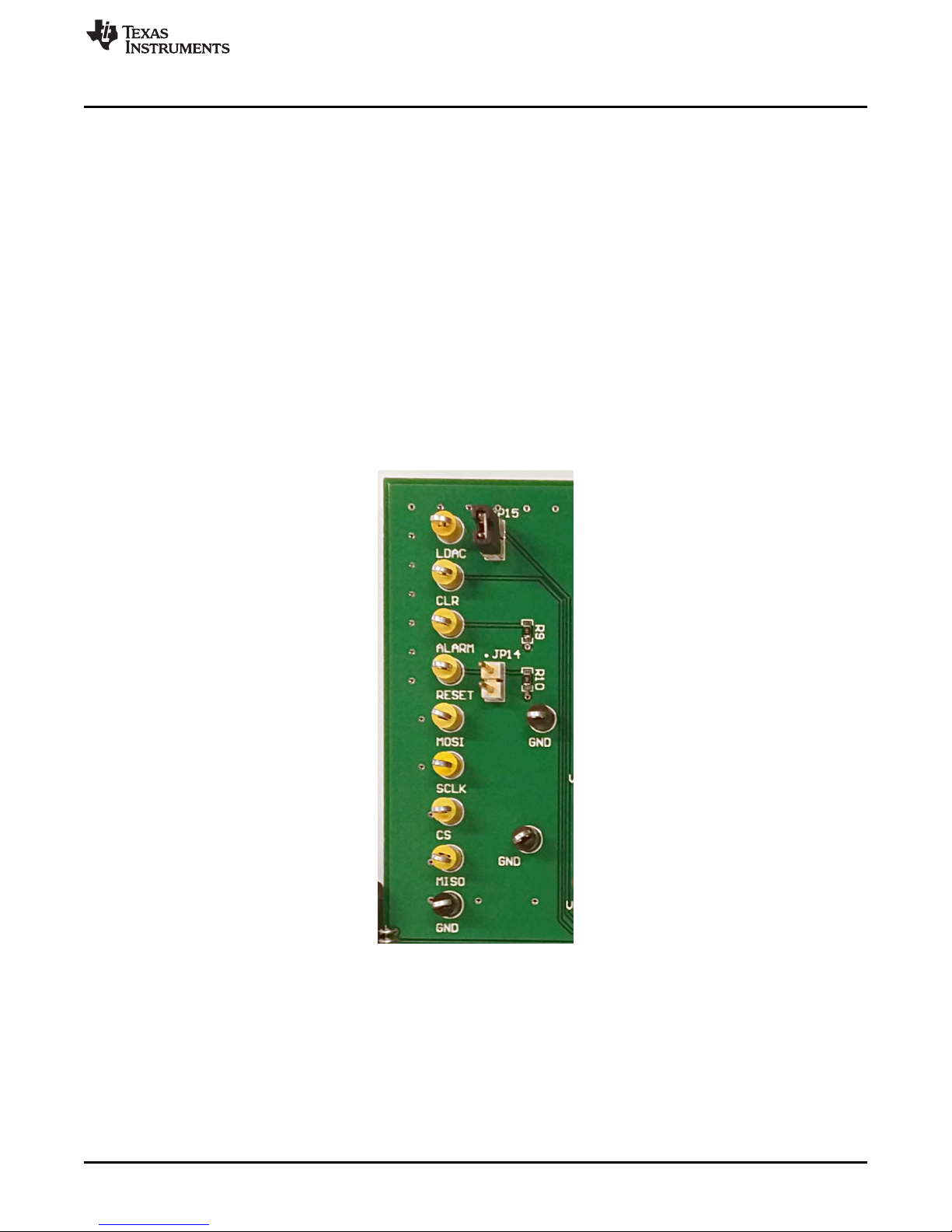
2.5.1 Communication Test Points
The EVM board features test points for monitoring the communication between the SM-USB-DIG and the
DAC8775. Test points are provided for the !LDAC, CLR, ALARM, RESET, SDIN, SCLK, !SYNC, and SDO
pins of the DAC8775.
EVM Hardware Overview
Figure 4. Digital Communication Test Points
The EVM design also allows external signals to be connected through these communication test points if
the EVM is integrated into a custom evaluation setup or application specific prototype. Note that if the SMUSB-DIG platform is not used, DVDD must be configured to use the DAC8775 internal DVDD LDO or
external supplies as described in Section 2.4.3.
SBAU248–November 2016
Submit Documentation Feedback
Copyright © 2016, Texas Instruments Incorporated
DAC8775EVM User’s Guide
7
Page 8
+
5
V
GND
EVM Hardware Overview
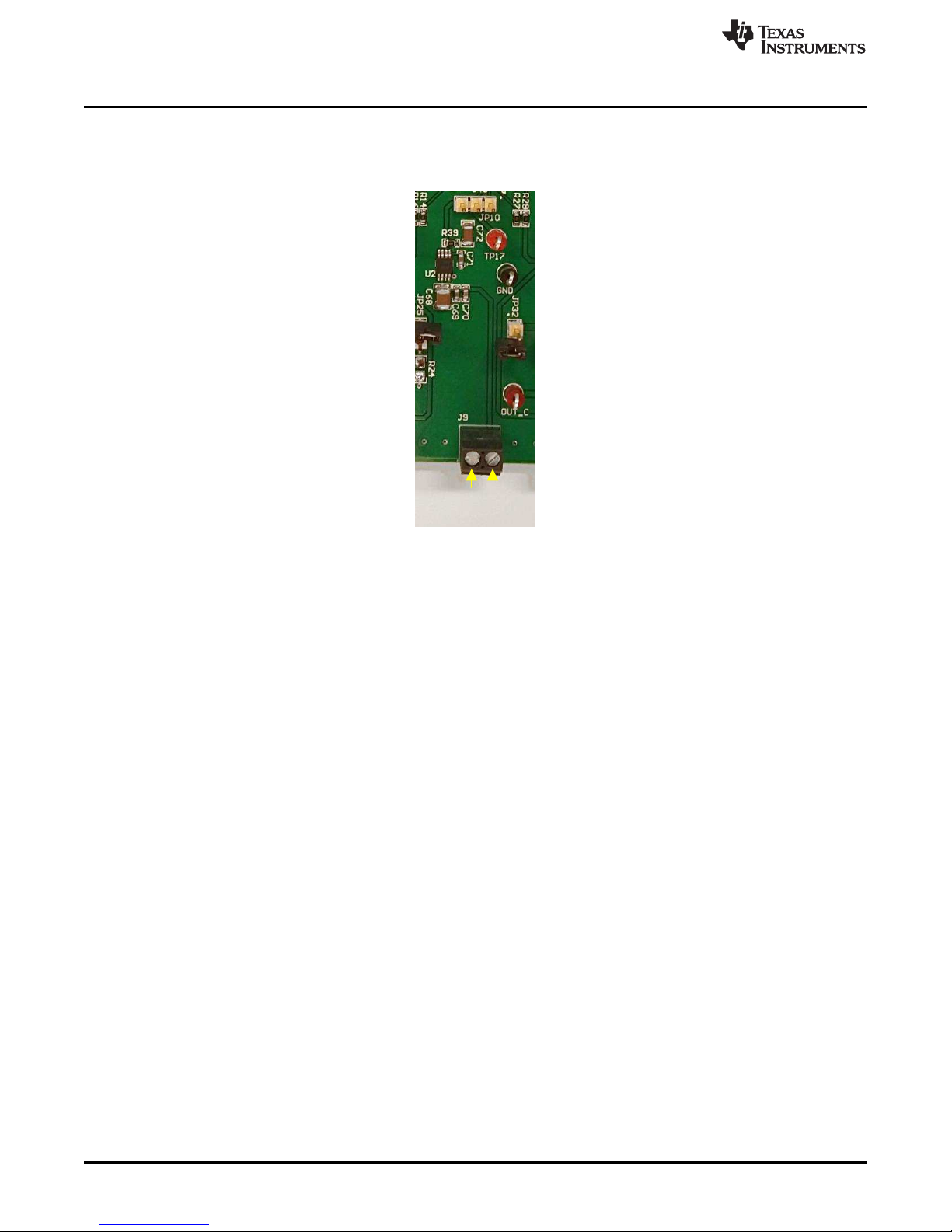
2.5.2 Reference Voltage
The DAC8775 reference voltage can be supplied by the internal voltage reference, by the onboard
REF5050, or by an external reference voltage.
www.ti.com
Figure 5. Onboard Reference Supply Connections
To use the internal reference voltage, place JP10 in the 1-2 position. To use the REF5050 reference
voltage, place JP10 in the 2-3 position and connect a supply voltage for the REF5050 to J9, as shown in
Figure 5. To use an external reference voltage, remove JP10 and the reference can be connected to the
DAC8775EVM through the center post of JP10.
2.5.3 VOUT_X, VSENSEP_X, and VSENSEN_X
The VOUT_X pins can be access on terminal blocks J5, J6, J7, and J8 or by the OUT_A, OUT_B,
OUT_C, or OUT_D test points. The VSENSEP_X and VSENSEN_X sense connections may be provided
onboard or externally closer to the point of load through terminal blocks J5, J6, J7, or J8. To provide the
VSENSEP_X connections onboard, install JP16, JP17, JP30, or JP31 based on the channel of interest.
Similarly, to provide VSENSEN_X connections onboard, install JP26, JP27, JP40, or JP41. Removing
these jumpers requires that the sense connections are made external to the EVM board. Figure 6 shows
the arrangement of the output terminal blocks.
2.5.4 IOUT_X
The IOUT_X pins can be accessed on terminal blocks J5, J6, J7, or J8 or by the test points OUT_A,
OUT_B, OUT_C, or OUT_D.
2.5.5 Onboard Output Loads
Four load choices are installed on the EVM board to evaluate the voltage and current outputs as well as
the adaptive power management performance of the DAC8775. JP18, JP22, JP32, or JP36 are available
to provide a short-circuit condition on the outputs. JP19, JP23, JP33, or JP37 provide a 250-Ω load on the
outputs. JP20, JP24, JP34, or JP38 are available to provide a 625-Ω on the outputs. JP21, JP25, JP35, or
JP39 provides a 1-kΩ load on the outputs.
8
DAC8775EVM User’s Guide
Copyright © 2016, Texas Instruments Incorporated
SBAU248–November 2016
Submit Documentation Feedback
Page 9

Load
Jumpers
GND
VSENSEN
_
A
VOUT
/
IOUT
_
A
VSENSEP
_
A
GND
VSENSEN
_B
VOUT
/
IOUT
_
B
VSENSEP
_
B
GND
VSENSEN
_
C
VOUT
/
IOUT
_
C
VSENSEP
_
C
GND
VSENSEN_
D
VOUT
/
IOUT
_
D
VSENSEP
_
D
www.ti.com
Figure 6. Output Terminal Block Connections and Load Jumpers
2.5.6 Applying HART Signals
JP28, JP29, JP42, and JP43 are available to couple external HART FSK communication signals onto the
current outputs. When injecting the HART signal, remove JP28, JP29, JP42, or JP43 and apply the HART
signal to pin 1. When a HART signal is not being injected, install JP28, JP29, JP42, or JP43, with AC
coupling the HART pins to ground.
EVM Hardware Overview
2.6 Connecting the SM-USB-DIG
To connect the EVM board and the SM-USB-DIG platform together, firmly slide the male and female ends
of the 10-pin connectors together with the Texas Instruments logo of the SM-USB-DIG facing up as shown
in Figure 7. Make sure that the two connectors are completely pushed together as loose connections may
cause intermittent operation.
SBAU248–November 2016
Submit Documentation Feedback
Figure 7. SM-USB-DIG Connection
Copyright © 2016, Texas Instruments Incorporated
DAC8775EVM User’s Guide
9
Page 10

EVM Hardware Overview
2.7 Signal Definitions of J1 (10-Pin SM-USB-DIG Connector)
Table 4 shows the pin-out for the 10-pin connector used to communicate between the EVM and the SM-
USB-DIG. Note that the I2C communication lines (I2C_SCL and I2C_SDA1) are not used.
Table 4. SM-USB-DIG Connector
PIN ON J1 SIGNAL DESCRIPTION
1 I2C_SCL I2C clock signal (SCL)
2 CTRL/MEAS4 GPIO: Control output or measure input
3 I2C_SDA1 I2C data signal (SDA)
4 CTRL/MEAS5 GPIO: Control output or measure input
5 SPI_DOUT1 SPI data output (MOSI)
6 VDUT
7 SPI_CLK SPI clock signal (SCLK)
8 GND Power return (GND)
9 SPI_CS1 SPI chip-select signal (!CS)
10 SPI_DIN1 SPI data input (MISO)
Switchable DUT power supply: 3.3 V, 5 V, Hi-Z (disconnected).
Note: When VDUT is Hi-Z, all digital I/Os are Hi-Z as well
3 EVM Software Setup
This section discusses how to install the EVM software.
www.ti.com
3.1 Operating Systems for EVM Software
The EVM software has been tested on the Windows XP®and Windows 7®operating systems with United
States and European regional settings. The software should also function on other Windows operating
systems.
3.2 EVM Software Installation
The EVM software may be downloaded by following the instructions provided external to this document.
To install the software, locate and extract the file named DAC8775.zip to a specific folder (for example,
C:\DAC8775\) on the hard drive.
10
DAC8775EVM User’s Guide
Figure 8. DAC8775EVM Installer
Copyright © 2016, Texas Instruments Incorporated
SBAU248–November 2016
Submit Documentation Feedback
Page 11
www.ti.com
After the files are extracted, navigate to the folder created on the hard drive. Locate and execute the
setup.exe file to start the installation. The DAC8775 software installer file then opens to begin the
installation process.
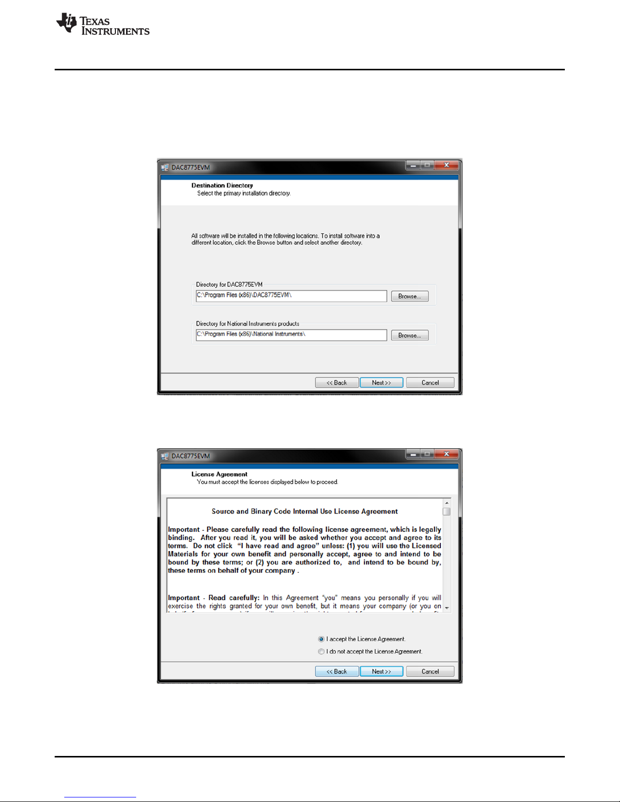
After the installation process initializes, the user is given a choice of selecting the installation directory,
usually defaulting to C:\Program Files(x86)\DAC8775EVM\ and C:\Program Files(x86)\National
Instruments\.
EVM Software Setup
Figure 9. DAC8775EVM Install Path
After selecting the installation directory, two license agreements are presented that must be accepted.
Figure 10. DAC8775EVM Software License Agreements
After accepting the Texas Instruments and National Instruments license agreements, the progress bar
opens and shows the installation of the software. Once the installation process is completed, click Finish.
SBAU248–November 2016
Submit Documentation Feedback
Copyright © 2016, Texas Instruments Incorporated
DAC8775EVM User’s Guide
11
Page 12

EVM Software Overview
4 EVM Software Overview
This section describes the use of the EVM software. Figure 11 shows the front panel of the EVM GUI.
www.ti.com
4.1 Starting the EVM Software
The EVM software can be operated through the Windows start menu. From the start menu, select All
Programs, and then select DAC8775EVM.
An error will appear if the PC cannot communicate with the EVM. If this error happens, first ensure that
the USB cable is properly connected on both ends. This error can also occur if the USB cable is
connected before the SM-USB-DIG platform power source. Another possible source for this error is a
problem with the USB human interface driver on the PC. Make sure the device is recognized when the
USB cable is plugged in, as indicated by a Windows-generated confirmation sound.
4.2 Reading From and Writing to Registers
The EVM software automatically reads from the DAC8775 when a reset or clear command is issued. To
read from the device in other situations, press the READ ALL button on the EVM GUI. Write actions are
carried out automatically when the value of any element on the GUI is changed.
12
DAC8775EVM User’s Guide
Figure 11. EVM GUI – Front Panel
Copyright © 2016, Texas Instruments Incorporated
SBAU248–November 2016
Submit Documentation Feedback
Page 13

www.ti.com
4.3 Device Controls
This section describes the GUI controls for the internal reference, power-on conditions, clear, software
reset, and DAC broadcast functionality.
4.3.1 Internal Reference
The internal reference can be enabled or disabled using the internal reference control on the EVM GUI. By
default, the internal reference is disabled.
4.3.2 Power-On Condition
By default the power-on state of the current output is Hi-Z and the voltage output is 30 kΩ to ground after
a clear or reset command. The power-on condition GUI control allows control of the voltage output poweron condition as either 30 kΩ to ground or Hi-Z.
4.3.3 Software Reset
The RESET button on the GUI issues a software reset to the DAC8775, restoring the default power-on
register contents. The GUI immediately reads all of the registers of the device to synchronize the GUI and
hardware. A hardware reset can be issued through JP14. If a hardware issue is issued the READ ALL
button should be pressed to synchronize the GUI and hardware.
4.3.4 Software Clear
The CLEAR button on the GUI issues a clear command to the DAC8775, restoring the DAC data registers
to full-scale or zero-scale based on each channel’s clear select settings and clear enable settings. After a
clear command is issued the GUI immediately reads the data registers of the device to synchronize the
GUI and hardware. A hardware clear command can be issued through JP12. If a hardware clear is issued
the READ ALL button should be pressed to synchronize the GUI and hardware.
EVM Software Overview
4.4 DAC Controls
4.4.1 DAC Outputs
The DACs can be configured for voltage or current outputs of various spans through the Output Mode
control on the GUI. The DAC output can be set to active or inactive by checking or removing the check
from the Output Enable Boolean control on the GUI. Once an output range is selected and the output is
enabled, the DAC output value can be controlled by writing values to the DAC Data control. The DAC
Data control expects hexadecimal input formats. The small indicator on the left side of the DAC Data
control can be used to change the input data format.
Output current drive can be programmatically limited for each of the voltage output modes through the
V
Current Limit control on the GUI. Take note that the actual current limit will be compliant to the values
OUT
specified in the DAC8775 electrical characteristics table.
4.4.2 Clear Functionality
Each DAC output has a Clear Enable Boolean that is AND’d with the CLEAR command. If the Clear
Enable Boolean is checked, the output channel will respond to a clear event; conversely, if the Boolean is
unchecked, the output channel will not respond to a clear event. Each DAC can be programmed to clear
to either zero-scale or full-scale. This behavior can be controlled by the Clear Select control on the GUI.
4.4.3 HART Inputs
The enable HART signals to be coupled to the current outputs through the onboard coupling path the
HART-Enable Boolean control must be checked.
SBAU248–November 2016
Submit Documentation Feedback
Copyright © 2016, Texas Instruments Incorporated
DAC8775EVM User’s Guide
13
Page 14

EVM Software Overview
4.5 DAC Calibration Controls
Each DAC may use digital calibration to reduce offset and gain errors at each channel’s output. By default
the calibration features are disabled. To enable the calibration features, the Calibration Enable Boolean
control must be checked. When the control is checked, offset and gain calibration may be controlled by
the values written to each channels Offset Calibration and Gain Calibration controls, respectively, on the
EVM GUI. For more information concerning the calibration features, please refer to the DAC8775
datasheet.
4.6 Slew-Rate Controls
The slew-rate of each channel may be controlled by the slew control registers for each channel. By default
the slew-rate control features are disabled. To enable the slew-rate control features the Slew-Rate Ctl
Enable Boolean control must be checked. When the control is checked, slew-rate step size and clock
registers may be used to control the output’s slew-rate through the Slew-Rate Ctl Step Size and SlewRate Ctl Clock respectively.
4.7 Buck-Boost Converter Controls
Each buck-boost converter can be configured through the EVM GUI. The Buck-Boost Mode control is
used to select the operating mode of the buck-boost converter and the Buck-Boost Enable control is used
to enable the positive, negative, or both arms of the buck-boost converter. When Buck-Boost Mode is set
to Clamp Mode, the positive clamp and negative clamp controls are used to set each arm’s output clamp.
www.ti.com
14
DAC8775EVM User’s Guide
Copyright © 2016, Texas Instruments Incorporated
SBAU248–November 2016
Submit Documentation Feedback
Page 15
VSENSEP_A
CCOMP_A
VOUT_A
IOUT_A
VSENSEN_A
HART_IN_A
VSENSEP_B
CCOMP_B
VOUT_B
IOUT_B
VSENSEN_B
HART_IN_B
VSENSEP_C
CCOMP_C
VOUT_C
IOUT_C
VSENSEN_C
HART_IN_C
VSENSEP_D
CCOMP_D
VOUT_D
IOUT_D
VSENSEN_D
HART_IN_D
1
2
3
JP10
5
4
1
2
3
6
7
8
9
10
SPI_DIN
SPI_CS
GND
SPI_CLK
VDUT
SPI_DOUT
CTRL/MEAS5
I2C_SDA
CTRL/MEAS4
I2C_SCK
J1
SUPER MINI DIG FEMALE
SPI_MISO
SPI_SCLK
SPI_CS
SPI_MOSI
RESET
DIG_DVDD
SPI_CS
SPI_MOSI
SPI_MISO
SPI_LDAC
SPI_SCLK
0.1µF
C43
EXT_VREF
12
JP9
12
JP11
DIG_DVDD
PVDD/AVDD
AGND_A
PVSS_A
PVDD_A
VPOS_IN_A
LN_A
LP_A
VNEG_IN_A
VNEG_IN_A
VPOS_IN_B
LN_B
LP_B
VNEG_IN_B
VNEG_IN_B
AGND_B
PVSS_B
PVDD_B
AGND_C
PVSS_C
PVDD_C
VPOS_IN_C
LN_C
LP_C
VNEG_IN_C
VNEG_IN_C
VPOS_IN_D
LN_D
LP_D
VNEG_IN_D
VNEG_IN_D
AGND_D
PVSS_D
PVDD_D
0.1µF
C41
LDAC CS MOSI MISO SCLK
SPI_CS
SPI_MOSI
SPI_MISO
SPI_LDAC
SPI_SCLK
ALARM
ALARM
ALARM
ALARM
DVDD
DVDD
1
2
JP14
10k
R10
1
2
J2
PVDD/AVDD
PVDD/AVDD
1
2
J3
AVSS
AVSS
GNDGND
GNDGNDGNDGND
GNDGNDGNDGND
AVSS
PVDD/AVDD
VREF_IN
10µF
C44
10µF
C45
10µF
C46
1µF
C42
1 2
JP13 DVDD
200pF
C47
DVDD
10k
R9
RESET
RESET
RESET
1
2
3
JP12
DVDD
CLR
CLR
CLR
1
2
JP15
DVDD
PVDD_D
1
LP_D
2
PVSS_D
3
LN_D
4
PVDD_C
5
LP_C
6
PVSS_C
7
LN_C
8
AGND_B
9
LN_B
10
PVSS_B
11
LP_B
12
PVDD_B
13
LN_A
14
PVSS_A
15
LP_A
16
PVDD_A
17
AGND_A
18
VNEG_IN_A
19
VNEG_IN_B
20
SCLK
21
SDIN
22
LDAC
23
SDO
24
SYNC
25
CLR
26
HARTIN_B
27
CCOMP_B
28
HARTIN_A
29
CCOMP_A
30
VSENSEP_B
31
VSENSEN_B
32
VSENSEP_A
33
VSENSEN_A
34
AGND2
35
VNEG_IN_A
36
IOUT_A
37
VPOS_IN_A
38
VOUT_A
39
VNEG_IN_B
40
IOUT_B
41
VPOS_IN_B
42
VOUT_B
43
AVDD
44
AGND3
45
REFIN
46
REFOUT
47
VOUT_C
48
VPOS_IN_C
49
IOUT_C
50
VNEG_IN_C
51
VOUT_D
52
VPOS_IN_D
53
IOUT_D
54
VNEG_IN_D
55
AGND1
56
VSENSEN_D
57
VSENSEP_D
58
VSENSEN_C
59
VSENSEP_C
60
CCOMP_D
61
HARTIN_D
62
CCOMP_C
63
HARTIN_C
64
DVDD_EN
65
DVDD
66
ALARM
67
RESET
68
AGND_D
69
VNEG_IN_C
70
VNEG_IN_D
71
AGND_C
72
EP
73
U1
DAC8775RMP
ALARM
RESET
CLR
SPI_LDAC
REFOUT
REFIN
REFIN
REFOUT
1
2
J4
DVDD
GND
GND
GND GND
GND
GND
GND
GND
GND
GND
GND
GND
GND
GND GND
GND
Copyright © 2016, Texas Instruments Incorporated
www.ti.com
5 EVM Documentation
This section contains the complete bill of materials and schematic diagram for the DAC8775EVM.
Documentation information for the SDM-USB-DIG Platform can be found in the SDM-USB-DIG Platform
User’s Guide (SBOU136) available at www.TI.com.
5.1 EVM Board Schematic
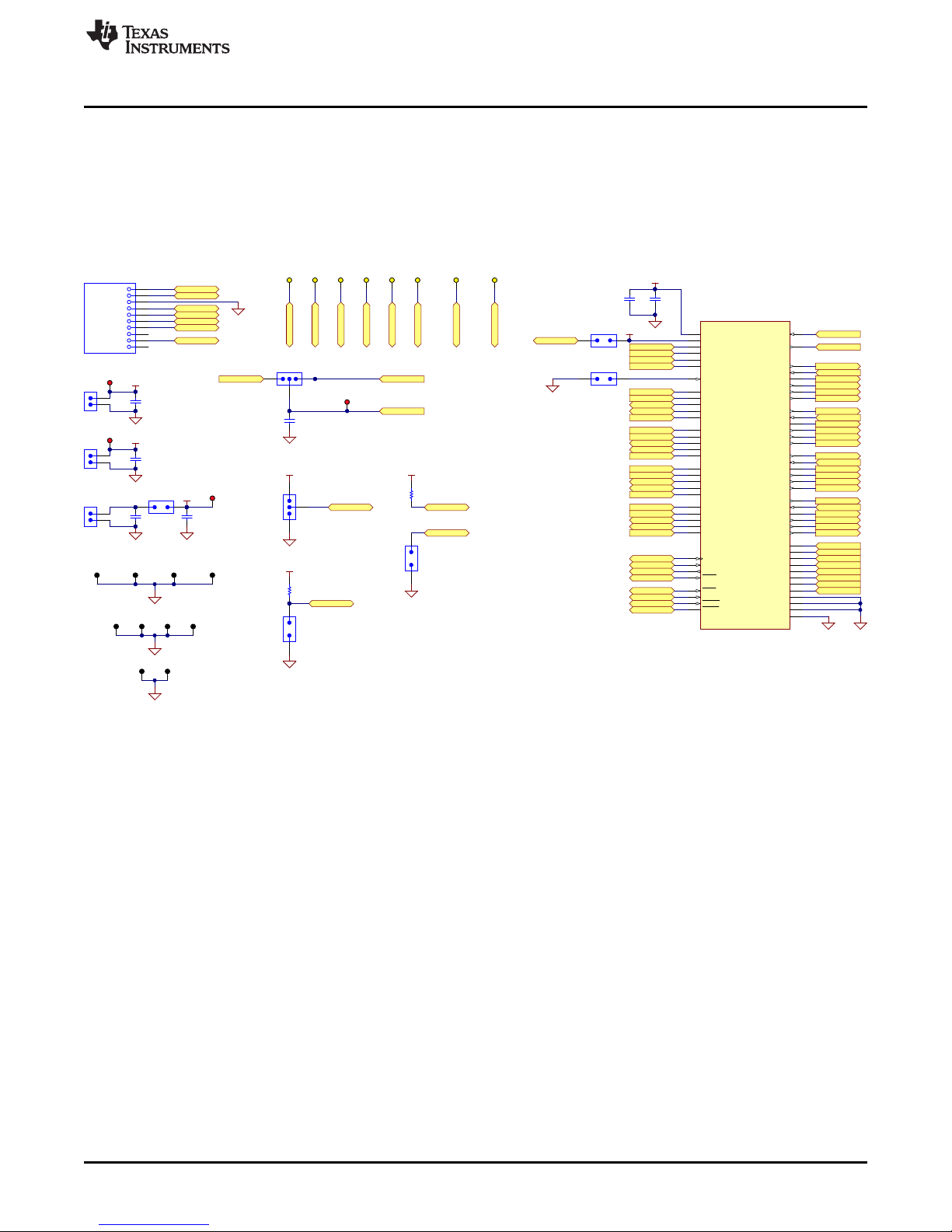
Figure 12, Figure 13, and Figure 14 illustrate the DAC8775EVM board schematics.
EVM Documentation
SBAU248–November 2016
Submit Documentation Feedback
Figure 12. Device Schematic
Copyright © 2016, Texas Instruments Incorporated
DAC8775EVM User’s Guide
15
Page 16

VSENSEP_A
CCOMP_A
VOUT_A
IOUT_A
VSENSEN_A
HART_IN_A
VSENSEP_B
CCOMP_B
VOUT_B
IOUT_B
VSENSEN_B
HART_IN_B
VSENSEP_C
CCOMP_C
VOUT_C
IOUT_C
VSENSEN_C
HART_IN_C
VSENSEP_D
CCOMP_D
VOUT_D
IOUT_D
VSENSEN_D
HART_IN_D
12
JP16
15
R11
C48
DNI
15
R13
15
R15
12
JP26
4
1
2
3
J5
ED555/4DS
VPOS_A
75V
1
3
2
D17
BAV99-7-F
0.1µF
C54
1
2
JP18
1
2
JP19
1
2
JP20
12
JP17
15
R12
C49
DNI
15
R14
15
R16
12
JP27
4
1
2
3
J6
ED555/4DS
VPOS_B
75V
1
3
2
D18
BAV99-7-F
0.1µF
C55
VNEG_A VNEG_B
12
JP30
15
R25
C58
DNI
15
R27
15
R29
12
JP40
4
1
2
3
J7
ED555/4DS
VPOS_C
75V
1
3
2
D21
BAV99-7-F
0.1µF
C64
VNEG_C
12
JP31
15
R26
C59
DNI
15
R28
15
R30
12
JP41
4
1
2
3
J8
ED555/4DS
VPOS_D
75V
1
3
2
D22
BAV99-7-F
0.1µF
C65
VNEG_D
DNC
1
VIN
2
TEMP
3
GND
4
TRIM/NR
5
VOUT
6
NC
7
DNC
8
U2
REF5050IDGK
1
2
J9
VREFSUPPLY
10uF
C68
0.1µF
C70
1.50
R39
47µF
C72
EXT_VREF
OUT_A OUT_B
OUT_C OUT_D
1µF
C69
1µF
C60
1µF
C61
1µF
C52
1µF
C53
1µF
C62
1µF
C63
1µF
C71
1µF
C51
1µF
C50
1
2
JP21
0.022µF
C56
0.022µF
C66
0.022µF
C57
0.022µF
C67
1
2
JP22
1
2
JP23
1
2
JP24
1
2
JP25
1
2
JP36
1
2
JP37
1
2
JP38
1
2
JP39
1
2
JP32
1
2
JP33
1
2
JP34
1
2
JP35
600 ohm
FB9
600 ohm
FB10
600 ohm
FB11
600 ohm
FB12
300
R17
300
R18
300
R32
300
R31
324
R23
324
R34
324
R37
324
R20
249
R19
249
R22
249
R33
249
R36
1.00k
R21
1.00k
R24
1.00k
R35
1.00k
R38
36V
D19
36V
D20
36V
D23
36V
D24
1
2
JP28
1
2
JP42
1
2
JP43
1
2
JP29
GND
GND GND GND
GND
GND
GND GND
GND
GND
GND GND
GND GND
GND
GND
GND
GND GND GND
GND
GND
GNDGND
GND
GND
GND GND
GND GND
GND
GND
GND GND GND
Copyright © 2016, Texas Instruments Incorporated
PVDD/AVDD
100µH
L1
AGND_A
PVSS_A
PVDD_A
VPOS_IN_A
LN_A
LP_A
VNEG_IN_A
VNEG_IN_A
2k ohm
FB1
2k ohm
FB2
0.1µF
C5
1
2
3
JP1
1
2
3
JP2PVDD/AVDD AVSS
VPOS_A VNEG_A
0.1µF
C6
VPOS_IN_B
LN_B
LP_B
VNEG_IN_B
VNEG_IN_B
AGND_B
PVSS_B
PVDD_B
AGND_C
PVSS_C
PVDD_C
VPOS_IN_C
LN_C
LP_C
VNEG_IN_C
VNEG_IN_C
VPOS_IN_D
LN_D
LP_D
VNEG_IN_D
VNEG_IN_D
AGND_D
PVSS_D
PVDD_D
PVDD/AVDD
100µH
L2
2k ohm
FB3
2k ohm
FB4
0.1µF
C7
1
2
3
JP3
1
2
3
JP4PVDD/AVDD AVSS
VPOS_B VNEG_B
0.1µF
C8
PVDD/AVDD
100µH
L3
2k ohm
FB5
2k ohm
FB6
0.1µF
C25
1
2
3
JP5
1
2
3
JP6PVDD/AVDD AVSS
VPOS_C VNEG_C
0.1µF
C26
PVDD/AVDD
100µH
L4
2k ohm
FB7
2k ohm
FB8
0.1µF
C27
1
2
3
JP7
1
2
3
JP8PVDD/AVDD AVSS
VPOS_D VNEG_D
0.1µF
C28
VPOS_A VNEG_A VPOS_B VNEG_B
VPOS_D VNEG_DVPOS_C VNEG_C
10µFC310µF
C4
10µF
C16
10µF
C23
10µF
C24
10µF
C36
10µF
C35
10µF
C15
10µFC110µF
C2
10µF
C21
10µF
C22
1µF
C9
1µF
C10
1µF
C17
1µF
C18
1µF
C13
1µF
C19
1µF
C11
1µF
C12
1µF
C14
1µF
C20
1µF
C37
1µF
C38
1µF
C33
1µF
C30
1µF
C29
1µF
C39
1µF
C31
1µF
C32
1µF
C34
1µF
C40
10.0
R1
10.0
R2
10.0
R3
10.0
R4
10.0
R5
10.0
R6
10.0
R7
10.0
R8
D1
D3
D2
D4
D9
D11
D10
D12
36V
D5
36V
D6
36V
D7
36V
D8
36V
D13
36V
D14
36V
D15
36V
D16
GND
GND GND
GND
GNDGNDGNDGND
GND
GND
GND GND
GND
GNDGNDGNDGND
GND
GND
GND GND GND GND
GND
GNDGND
GND
GND
GND GND GND GND
GND
GNDGND
GND
Copyright © 2016, Texas Instruments Incorporated
EVM Documentation
www.ti.com
16
DAC8775EVM User’s Guide
Figure 13. DC-DC Schematic
Copyright © 2016, Texas Instruments Incorporated
Figure 14. Outputs Schematic
SBAU248–November 2016
Submit Documentation Feedback
Page 17

www.ti.com
5.2 EVM PCB Components Layout
Figure 15 shows the layout of the components for the EVM board.
EVM Documentation
Figure 15. DAC8775EVM PCB Components Layout
SBAU248–November 2016
Submit Documentation Feedback
Copyright © 2016, Texas Instruments Incorporated
DAC8775EVM User’s Guide
17
Page 18

EVM Documentation
5.3 EVM Board Bill of Materials
Table 5 lists the EVM board bill of materials.
QTY DESIGNATOR DESCRIPTION PARTNUMBER MANUFACTURER
1 !PCB1 Printed Circuit Board PA005 Any
15
15
31
12
10
33
C1, C2, C3, C4, C15, C16, C21, C22,
C23, C24, C35, C36, C44, C45, C46
C5, C6, C7, C8, C25, C26, C27, C28,
C41, C43, C54, C55, C64, C65, C70
C9, C10, C11, C12, C13, C14, C17,
C18, C19, C20, C29, C30, C31, C32,
C33, C34, C37, C38, C39, C40, C42,
C50, C51, C52, C53, C60, C61, C62,
C63, C69, C71
1 C47
4 C48, C49, C58, C59 DNI
4 C56, C57, C66, C67
1 C68
1 C72
8 D1, D2, D3, D4, D9, D10, D11, D12
D5, D6, D7, D8, D13, D14, D15, D16,
D19, D20, D23, D24
4 D17, D18, D21, D22
FB1, FB2, FB3, FB4, FB5, FB6, FB7,
8
FB8
4 FB9, FB10, FB11, FB12
1 J1
4 J2, J3, J4, J9
4 J5, J6, J7, J8
JP1, JP2, JP3, JP4, JP5, JP6, JP7,
JP8, JP10, JP12
JP9, JP11, JP13, JP14, JP15, JP16,
JP17, JP18, JP19, JP20, JP21, JP22,
JP23, JP24, JP25, JP26, JP27, JP28,
JP29, JP30, JP31, JP32, JP33, JP34,
JP35, JP36, JP37, JP38, JP39, JP40,
JP41, JP42, JP43
4 L1, L2, L3, L4
8 R1, R2, R3, R4, R5, R6, R7, R8
2 R9, R10
Table 5. EVM Board Bill of Materials
CAP, CERM, 10uF, 50V, +/10%, X7R, 1210 (H=2.5mm)
CAP, CERM, 0.1uF, 50V, +/10%, X7R, 0603
CAP, CERM, 1uF, 50V, +/10%, X7R, 0603
CAP, CERM, 200pF, 50V, +/5%, C0G/NP0, 0603
CAP, CERM, 0.022uF, 50V,
+/-10%, X7R, 0603
CAP CER 10UF 50V 20%
X7R 1210
CAP, CERM, 47uF, 25V, +/20%, X5R, 1206
Diode, Schottky, 60V, 1A,
SOD-123
Diode, TVS, Bi, 36V, 400W,
SOD323, 2-Leads, Body
1.9x1.45mm, No Polarity
Mark
Diode, Switching, 75V, 0.3A,
SOT-23
Ferrite Bead, 2000 ohm @
100MHz, 1.2A, 1210
(H=2.5mm)
Ferrite Bead, 600 ohm @
100MHz, 3A, 1210
(H=2.5mm)
Receptacle, 50mil 10x1, R/A,
TH
Terminal Block, 6A, 3.5mm
Pitch, 2-Pos, TH
Terminal Block, 6A, 3.5mm
Pitch, 4-Pos, TH
Header, TH, 100mil, 3x1,
Gold plated, 230 mil above
insulator
Header, TH, 100mil, 2x1,
Gold plated, 230 mil above
insulator
Inductor, Shielded Drum
Core, Ferrite, 100uH, 0.52A,
0.77 ohm, SMD
RES, 10.0 ohm, 1%, 0.1W,
0603
RES, 10k ohm, 5%, 0.1W,
0603
UMK325AB7106KM-T Taiyo Yuden
GRM188R71H104KA93
D
UMK107AB7105KA-T Taiyo Yuden
GRM1885C1H201JA01
D
C1608X7R1H223K TDK
UMK325AB7106MM-T Taiyo Yuden
C3216X5R1E476M160A
C
MBRX160-TP
CDSOD323-T36SC Bourns
BAV99-7-F Diodes Inc.
FB MH3225HM202NT Taiyo Yuden
FBMH3225HM601NT Taiyo Yuden
851-43-010-20-001000 Mill-Max
ED555/2DS
ED555/4DS
TSW-103-07-G-S Samtec, Inc.
TSW-102-07-G-S Samtec
74408943101
CRCW060310R0FKEA Vishay-Dale
CRCW060310K0JNEA Vishay-Dale
www.ti.com
MuRata
MuRata
TDK
Micro Commercial
Components
On-Shore
Technology
On-Shore
Technology
Wurth Elektronik
eiSos
18
DAC8775EVM User’s Guide
SBAU248–November 2016
Submit Documentation Feedback
Copyright © 2016, Texas Instruments Incorporated
Page 19

www.ti.com
EVM Documentation
Table 5. EVM Board Bill of Materials (continued)
QTY DESIGNATOR DESCRIPTION PARTNUMBER MANUFACTURER
12
16
10
R11, R12, R13, R14, R15, R16, R25,
R26, R27, R28, R29, R30
4 R17, R18, R31, R32
4 R19, R22, R33, R36
4 R20, R23, R34, R37
4 R21, R24, R35, R38
1 R39
TP1, TP2, TP3, TP4, TP5, TP6, TP7,
TP8, TP17, TP18, TP19, TP20, TP31,
TP32, TP33, TP34
TP9, TP10, TP11, TP12, TP13, TP14,
8
TP15, TP16
TP21, TP22, TP23, TP24, TP25,
TP26, TP27, TP28, TP29, TP30
1 U1
1 U2
1 U2
RES, 15 ohm, 5%, 0.1W,
0603
RES, 300, 0.1%, 0.25 W,
1206
RES, 249, 0.1%, 0.25 W,
1206
RES, 324, 0.1%, 0.25 W,
1206
RES, 1.00 k, 0.1%, 1 W, 1206
resistor
RES, 1.50 ohm, 1%, 0.1W,
0603
Test Point, Compact, Red, TH 5005 Keystone
Test Point, Compact, Yellow,
TH
Test Point, Compact, Black,
TH
Quad-Channel, 16-Bit
Programmable Current
Output and Voltage Output
Digital-to-Analog Converter
with Adaptive Power
Management, RMP0072A
Low-Noise, Very Low Drift,
Precision Voltage Reference,
DGK0008A
Low-Noise, Very Low Drift,
Precision Voltage Reference,
DGK0008A
CRCW060315R0JNEA Vishay-Dale
ERA-8AEB301V Panasonic
TNPW1206249RBEEA Vishay-Dale
ERA-8AEB3240V Panasonic
PHP01206E1001BST5 Vishay-Dale
CRCW06031R50FKEA Vishay-Dale
5009 Keystone
5006 Keystone
DAC8775RMP Texas Instruments
REF5050IDGK Texas Instruments
REF5050IDGK Texas Instruments
SBAU248–November 2016
Submit Documentation Feedback
Copyright © 2016, Texas Instruments Incorporated
DAC8775EVM User’s Guide
19
Page 20

IMPORTANT NOTICE
Texas Instruments Incorporated and its subsidiaries (TI) reserve the right to make corrections, enhancements, improvements and other
changes to its semiconductor products and services per JESD46, latest issue, and to discontinue any product or service per JESD48, latest
issue. Buyers should obtain the latest relevant information before placing orders and should verify that such information is current and
complete. All semiconductor products (also referred to herein as “components”) are sold subject to TI’s terms and conditions of sale
supplied at the time of order acknowledgment.
TI warrants performance of its components to the specifications applicable at the time of sale, in accordance with the warranty in TI’s terms
and conditions of sale of semiconductor products. Testing and other quality control techniques are used to the extent TI deems necessary
to support this warranty. Except where mandated by applicable law, testing of all parameters of each component is not necessarily
performed.
TI assumes no liability for applications assistance or the design of Buyers’ products. Buyers are responsible for their products and
applications using TI components. To minimize the risks associated with Buyers’ products and applications, Buyers should provide
adequate design and operating safeguards.
TI does not warrant or represent that any license, either express or implied, is granted under any patent right, copyright, mask work right, or
other intellectual property right relating to any combination, machine, or process in which TI components or services are used. Information
published by TI regarding third-party products or services does not constitute a license to use such products or services or a warranty or
endorsement thereof. Use of such information may require a license from a third party under the patents or other intellectual property of the
third party, or a license from TI under the patents or other intellectual property of TI.
Reproduction of significant portions of TI information in TI data books or data sheets is permissible only if reproduction is without alteration
and is accompanied by all associated warranties, conditions, limitations, and notices. TI is not responsible or liable for such altered
documentation. Information of third parties may be subject to additional restrictions.
Resale of TI components or services with statements different from or beyond the parameters stated by TI for that component or service
voids all express and any implied warranties for the associated TI component or service and is an unfair and deceptive business practice.
TI is not responsible or liable for any such statements.
Buyer acknowledges and agrees that it is solely responsible for compliance with all legal, regulatory and safety-related requirements
concerning its products, and any use of TI components in its applications, notwithstanding any applications-related information or support
that may be provided by TI. Buyer represents and agrees that it has all the necessary expertise to create and implement safeguards which
anticipate dangerous consequences of failures, monitor failures and their consequences, lessen the likelihood of failures that might cause
harm and take appropriate remedial actions. Buyer will fully indemnify TI and its representatives against any damages arising out of the use
of any TI components in safety-critical applications.
In some cases, TI components may be promoted specifically to facilitate safety-related applications. With such components, TI’s goal is to
help enable customers to design and create their own end-product solutions that meet applicable functional safety standards and
requirements. Nonetheless, such components are subject to these terms.
No TI components are authorized for use in FDA Class III (or similar life-critical medical equipment) unless authorized officers of the parties
have executed a special agreement specifically governing such use.
Only those TI components which TI has specifically designated as military grade or “enhanced plastic” are designed and intended for use in
military/aerospace applications or environments. Buyer acknowledges and agrees that any military or aerospace use of TI components
which have not been so designated is solely at the Buyer's risk, and that Buyer is solely responsible for compliance with all legal and
regulatory requirements in connection with such use.
TI has specifically designated certain components as meeting ISO/TS16949 requirements, mainly for automotive use. In any case of use of
non-designated products, TI will not be responsible for any failure to meet ISO/TS16949.
Products Applications
Audio www.ti.com/audio Automotive and Transportation www.ti.com/automotive
Amplifiers amplifier.ti.com Communications and Telecom www.ti.com/communications
Data Converters dataconverter.ti.com Computers and Peripherals www.ti.com/computers
DLP® Products www.dlp.com Consumer Electronics www.ti.com/consumer-apps
DSP dsp.ti.com Energy and Lighting www.ti.com/energy
Clocks and Timers www.ti.com/clocks Industrial www.ti.com/industrial
Interface interface.ti.com Medical www.ti.com/medical
Logic logic.ti.com Security www.ti.com/security
Power Mgmt power.ti.com Space, Avionics and Defense www.ti.com/space-avionics-defense
Microcontrollers microcontroller.ti.com Video and Imaging www.ti.com/video
RFID www.ti-rfid.com
OMAP Applications Processors www.ti.com/omap TI E2E Community e2e.ti.com
Wireless Connectivity www.ti.com/wirelessconnectivity
Mailing Address: Texas Instruments, Post Office Box 655303, Dallas, Texas 75265
Copyright © 2016, Texas Instruments Incorporated
 Loading...