

Page 1

User's Guide
SLAU700A–June 2017–Revised November 2017
DAC8742H Evaluation Module
This user's guide describes the characteristics, operation, and use of the DAC8742H evaluation board
(EVM). This user’s guide also discusses the proper setup and configuration of both software and
hardware, and reviews various aspects of program operation. A complete circuit description, schematic
diagram, and bill of materials are also included in this document.
Contents
1 Overview...................................................................................................................... 3
1.1 DAC8742HEVM Kit Contents ..................................................................................... 3
1.2 Related Documentation From Texas Instruments.............................................................. 3
2 DAC8742HEVM Hardware Setup ......................................................................................... 4
2.1 DAC8742H Hardware Theory of Operation ..................................................................... 4
2.2 USB2ANY Signal Definition ....................................................................................... 5
3 DAC8742HEVM Software Setup .......................................................................................... 6
3.1 Operating Systems for DAC8742HEVM Software.............................................................. 6
3.2 DAC8742H Software Installation ................................................................................. 6
4 DAC8742HEVM Hardware Overview ..................................................................................... 7
4.1 Electrostatic Discharge Warning.................................................................................. 7
4.2 Connecting the Hardware.......................................................................................... 7
4.3 DAC8742HEVM Power Configurations .......................................................................... 7
4.4 DAC8742H Reference Connection............................................................................... 8
4.5 Digital Inputs......................................................................................................... 8
4.6 Clock Configuration................................................................................................. 9
4.7 HART/PAFF Shunt Selection .................................................................................... 10
5 DAC8742HEVM Software Overview .................................................................................... 11
5.1 Starting the DAC8742HEVM Software ......................................................................... 11
5.2 DAC8742HEVM Software Features ............................................................................ 12
6 DAC8742HEVM Documentation ......................................................................................... 16
6.1 DAC8742HEVM Board Schematic.............................................................................. 17
6.2 DAC8742HEVM PCB Components Layout.................................................................... 18
6.3 DAC8742H Test Board Bill of Materials........................................................................ 19
1 DAC8742HEVM Hardware Setup ......................................................................................... 4
2 DAC8742H Test Board Block Diagram................................................................................... 4
3 Launching Software Setup ................................................................................................. 6
4 DAC8742HEVM GUI Location............................................................................................ 11
5 DAC8742HEVM GUI – Power On ....................................................................................... 11
6 DAC8742H EVM Software Page Selection............................................................................. 12
7 Low Level Configuration Page............................................................................................ 13
8 Low Level Configuration Page Available Options...................................................................... 13
9 High Level Configuration Page........................................................................................... 14
10 MODE Section.............................................................................................................. 15
11 DAC8742HEVM Digital Input Selection ................................................................................. 15
12 HART/PAFF Write/Read Control and Indicator Section............................................................... 16
13 DAC8742HEVM Board Schematic....................................................................................... 17
SLAU700A–June 2017–Revised November 2017
Submit Documentation Feedback
List of Figures
Copyright © 2017, Texas Instruments Incorporated
DAC8742H Evaluation Module
1
Page 2

14 DAC8742HEVM PCB Components Layout............................................................................. 18
1 Contents of DAC8742H Kit................................................................................................. 3
2 Related Documentation..................................................................................................... 3
3 J2 USB2ANY and Digital Signal Definition............................................................................... 5
4 Default Jumper Settings .................................................................................................... 7
5 DAC8742HEVM Power Supply Configuration ........................................................................... 7
6 DAC8742HEVM Reference Connection .................................................................................. 8
7 Digital Signal Definition ..................................................................................................... 8
8 J6 Digital Signal Definition.................................................................................................. 8
9 Clock Configuration.......................................................................................................... 9
10 XTAL1 and XTAL2 Configuration Settings ............................................................................... 9
11 Internal Mode Shunt Selection ........................................................................................... 10
12 External Filter Mode With Internal REF Shunt Selection ............................................................. 10
13 DAC8742H Test Board Bill of Materials................................................................................. 19
Trademarks
Microsoft, Windows are registered trademarks of Microsoft Corporation.
LabVIEW is a trademark of National Instruments Corporation.
All other trademarks are the property of their respective owners.
www.ti.com
List of Tables
2
DAC8742H Evaluation Module
Copyright © 2017, Texas Instruments Incorporated
SLAU700A–June 2017–Revised November 2017
Submit Documentation Feedback
Page 3

www.ti.com
1 Overview
This EVM features the DAC8742H device, which is a Highway Addressable Remote Transducer (HART),
FOUNDATION Fieldbus (FF), and Profibus process automation (PA) compliant low-power frequency-shift
keying (FSK) modem designed for industrial process control and industrial automation applications. The
device includes an integrated receive band-pass filter, flexible clocking options and can operate from a
1.8- to 5.5-V range. The wide temperature range, –55°C to 125°C, and low quiescent current make this
device an ideal candidate for smart transmitters, programmable-logic controller (PLC) I/O modules, and
other industrial process-control applications.
1.1 DAC8742HEVM Kit Contents
Table 1 details the contents of the kit. Contact the TI Product Information Center or visit the Texas
Instruments E2E Community (http://E2E.ti.com) if any component is missing. TI highly recommends that
the user verify the latest versions of the related software at the TI website, www.ti.com.
Table 1. Contents of DAC8742H Kit
Item Quantity
DAC8742HEVM PCB evaluation board 1
USB2ANY 1
1.2 Related Documentation From Texas Instruments
The following document provides information regarding Texas Instruments integrated circuits used in the
assembly of the DAC8742HEVM. This user's guide is available from the TI web site under literature
number SLAU700. Any letter appended to the literature number corresponds to the document revision that
is current at the time of the writing of this document. Newer revisions may be available from the TI web
site at http://www.ti.com/, or call the Texas Instruments Literature Response Center at (800) 477-8924 or
the Product Information Center at (972) 644-5580. When ordering, identify the document by both title and
literature number.
Overview
Table 2. Related Documentation
Document Literature Number
DAC8742H data sheet SBAS856
USB2ANY SBOU136
SLAU700A–June 2017–Revised November 2017
Submit Documentation Feedback
Copyright © 2017, Texas Instruments Incorporated
DAC8742H Evaluation Module
3
Page 4
(Optional)
External/Onboard REF
USB2ANY
Connection
(HART/PAFF)
TX/RX
Optional External Power
(AVDD/IOVDD)
DAC8742H
SPI
Power
Copyright © 2017, Texas Instruments Incorporated
DAC8742HEVM
USB Bus
from
Computer
(Optional) External
Power Source
LaunchPad
Connector
USB2ANY
Personal
Computer
(PC)
Copyright © 2017, Texas Instruments Incorporated
DAC8742HEVM Hardware Setup
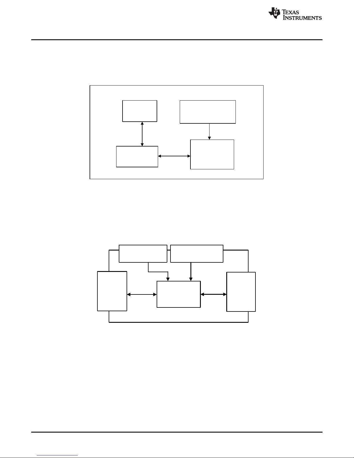
2 DAC8742HEVM Hardware Setup
This section provides the overall system setup for the EVM. A PC runs software that communicates with
the USB2ANY platform, which generates the optional IOVDD or AVDD power and digital signals used to
communicate with the EVM board. Test point connections are included on the EVM board for external
power supplies. Figure 1 displays the DAC8742HEVM system setup.
Figure 1. DAC8742HEVM Hardware Setup
www.ti.com
2.1 DAC8742H Hardware Theory of Operation
A block diagram of the DAC8742HEVM PCB board is displayed in Figure 2. The EVM board provides an
interface to optional external supplies, an external reference, and a USB2ANY connection for serial
peripheral interface (SPI) and universal asynchronous receiver and transmitter (UART) communication.
Figure 2. DAC8742H Test Board Block Diagram
4
DAC8742H Evaluation Module
Copyright © 2017, Texas Instruments Incorporated
SLAU700A–June 2017–Revised November 2017
Submit Documentation Feedback
Page 5

www.ti.com
2.2 USB2ANY Signal Definition
The DAC8742HEVM provides a hardware connector (J2) that connects to the USB2ANY interface board,
which can supply IOVDD and AVDD power and is responsible for providing the SPI or UART commands
sent from the PC GUI software. Optionally, provide the AVDD and IOVDD supply through an external
supply, and access all digital communication lines through their respective digital test points. This
information is provided in Table 3.
Table 3. J2 USB2ANY and Digital Signal Definition
Pin On J2 Signal Description
2 COM_SELECT Select between SPI or UART
4, 6, 8, 16, 27, 28 GND CS | general purpose I/O
12 CS_GPIO6 SPI, CS, or general purpose I/O
13 RXD_MISO UART RXD or SPI MISO
14 TXD_MOSI UART TXD or SPI MOSI
15 USB 3.3V 3.3-V USB power
18 SCLK_GPIO2 SPI SCLK or general purpose I/O
25 REF_EN DAC8742H reference enable
26 IF_SEL DAC8742H IF_SEL pin
29 BPF_EN General purpose I/O
30 RST DAC8742H rest Line
DAC8742HEVM Hardware Setup
SLAU700A–June 2017–Revised November 2017
Submit Documentation Feedback
Copyright © 2017, Texas Instruments Incorporated
DAC8742H Evaluation Module
5
Page 6
DAC8742HEVM Software Setup
3 DAC8742HEVM Software Setup
This section provides the procedures for software installation.
3.1 Operating Systems for DAC8742HEVM Software
The EVM software has been tested on the Microsoft®Windows®XP and Windows 7 operating systems
with the United States and European regional settings. The software should also be compatible with other
Windows operating systems.
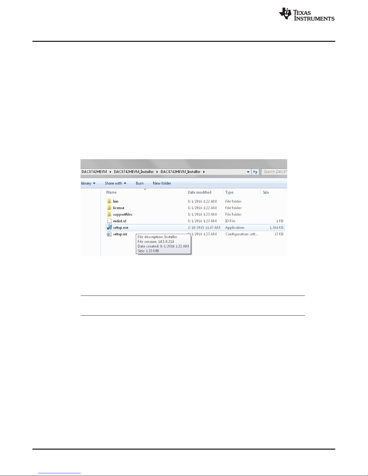
3.2 DAC8742H Software Installation
The software is available through the EVM product folder on the TI website. Once the software is
downloaded onto the PC, navigate to the DAC8742HEVM folder, and run the setup.exe file, as shown in
Figure 3. When the software is launched, an installation dialog will open, and prompt the user to select an
installation directory. If left unchanged, the software location defaults to C:\Program Files (x86)
\DAC8742HEVM.
www.ti.com
Figure 3. Launching Software Setup
The software installation will automatically copy the required LabVIEW™ software files and drivers to the
local machine.
NOTE: Verify that the USB2ANY is not connected before the software installation, as this may affect
file or driver installation.
6
DAC8742H Evaluation Module
Copyright © 2017, Texas Instruments Incorporated
SLAU700A–June 2017–Revised November 2017
Submit Documentation Feedback
Page 7

www.ti.com
4 DAC8742HEVM Hardware Overview
The subsequent sections provide detailed information on the EVM hardware, and jumper configuration
settings. Table 4 displays the default configurations of all jumper connections on the DAC8742HEVM.
Connect the USB extender cable from the USB2ANY to the PC.
Table 4. Default Jumper Settings
Jumper Position Description
JP1 Shunt on 1 – 2 HART: Connects to 3.6864-MHz external crystal
JP2 Shunt on 1 – 2 HART: Connects to 3.6864-MHz external crystal
JP4 Shunt on 2 – 3 Connects TS5N412PW device
JP5 Populate HART: Connects IOVDD to AVDD for single supply
JP6 Shunt on 1 – 2 Connects IOVDD to USB2ANY 3.3-V supply
JP8 Populate HART: Connects to 0.022-µF load capacitor
JP9 Shunt on 2 – 3 HART: Connects to MOD_IN
JP10 Shunt on 2 – 3 HART: Connects to 2200 pF
JP11 Shunt on 1 – 2 HART: Connects to 2200 pF
JP14 Shunt on 2 – 3 CLK_CFG1 set to GND
JP16 Shunt on 5 – 6 HART: Connects to 680 pF
JP17 Populate CLK_CFG0 set to GND
JP20 Shunt on 1 – 2 /XEN set to GND
DAC8742HEVM Hardware Overview
operation
4.1 Electrostatic Discharge Warning
Many of the components on the DAC8742HEVM are susceptible to damage by electrostatic discharge
(ESD). Customers are advised to observe proper ESD handling precautions when unpacking and handling
the board, including the use of a grounded wrist strap at an approved ESD workstation.
4.2 Connecting the Hardware
To connect the USB2ANY to the EVM board, align and firmly connect the keyed ribbon connector to the
J2 connector. Verify the connection is snug, as loose connections may cause intermittent operation.
4.3 DAC8742HEVM Power Configurations
The DAC8742HEVM provides electrical connections to the device supply pins. The connectors and
optional configurations are shown in the Table 5.
Table 5. DAC8742HEVM Power Supply Configuration
Connector Connection Type Description
J3 AVDD terminal block Connects external supply to AVDD net
J4 IOVDD terminal block Connects external supply to IOVDD net
JP5 Shunt connection Connects AVDD to IOVDD
JP6
USB2ANY can supply IOVDD and AVDD by populating the JP6 shunt to position (1 – 2) and connecting
shunt J5.
Shunt (1 – 2) Connects USB2ANY 3.3 V to IOVDD
Shunt (2 – 3) Connects IOVDD net to J4 terminal block
SLAU700A–June 2017–Revised November 2017
Submit Documentation Feedback
Copyright © 2017, Texas Instruments Incorporated
DAC8742H Evaluation Module
7
Page 8
DAC8742HEVM Hardware Overview
4.4 DAC8742H Reference Connection
The DAC8742HEVM connects to an optional external reference through the J5 terminal block, or it can be
supplied by the internal reference of the DAC8742H device (see Table 6).
Table 6. DAC8742HEVM Reference Connection
Connector Connection Type Description
J5 REF Terminal Block Connects external reference to REF net
JP7 Populate Connects external reference to REF net
4.5 Digital Inputs
The digital communication lines of the DAC8742H device can be accessed through the USB2ANY header
connection (J2) or the J6 header block, which are listed in Table 7 and Table 8, along with the digital input
signals of the DAC8742H device.
Table 7. Digital Signal Definition
Name Connector Description
JP13 IF_SEL
JP15, JP17 CLK_CFG0
JP14 CLK_CFG1
JP20 /XEN
JP19 REF_EN
JP18 BPF_EN
www.ti.com
(1 – 2) IOVDD: SPI mode
(2 – 3) GND: UART mode
(JP15 – closed, JP17 – open): CLK_CFG0 set to IOVDD
(JP15 – open, JP17 – closed): CLK_CFG0 set to GND
(JP15 – closed, JP17 – closed): CLK_CFG0 set to (0.5) IOVDD
(1 – 2) CLK_CFG1 set to IOVDD
(2 – 3) CLK_CFG1 set to GND
(1 – 2) GND: external crystal
(2 – 3) IOVDD: external oscillator or internal oscillator required
(1 – 2) GND: external reference
(2 – 3) IOVDD: internal reference
(1 – 2) GND: external bandpass required
(2 – 3) IOVDD: internal bandpass filter
Name Connector
J6-1 UART_OUT/SDO
J6-2 DUPLEX/SDI
J6-3 /UART_RTS/SCLK
J6-4 UART_IN/CS
J6-5 CD/IRQ
J6-6 /RST
J6-7 IOVDD
J6-8 GND
NOTE: Control the REF_EN, BPF_EN, and IF_SEL lines through the GUI.
The DAC8742H data sheet lists acceptable clock configurations, and they are also listed in Table 9 for
reference.
8
DAC8742H Evaluation Module
Table 8. J6 Digital Signal Definition
Copyright © 2017, Texas Instruments Incorporated
SLAU700A–June 2017–Revised November 2017
Submit Documentation Feedback
Page 9
www.ti.com
4.6 Clock Configuration
The DAC8742H device supports a variety of clocking options in order to provide system flexibility and
reduce overall current consumption in HART applications. The clocking options include: an internal
oscillator (HART mode only), an external crystal oscillator, or an external CMOS clock.
Configure clock selection via the XEN, CLK_CFG1, and CLK_CFG0 pins (see Table 9).
XEN CLK_CFG1 CLK_CFG0 CLKO Description Mode
1 0 0 No output 3.6864-MHz CMOS clock connected at XTAL1
1 0 1 No output 1.2288-MHz CMOS clock connected at XTAL1
1 1 0 No output Internal oscillator enabled
1 1 1 1.2288-MHz output Internal oscillator enabled, CLKO enabled
0 0 0 No output Crystal oscillator enabled
0 0 1 3.6864-MHz output 3.6864-MHz crystal oscillator, CLKO enabled
0 1 0 1.8432-MHz output 1.8432-MHz crystal oscillator, CLKO enabled
0 1 1 1.2288-MHz output 1.2288-MHz crystal oscillator, CLKO enabled
1 0 0.5 × IOVDD No output 4-MHz CMOS clock connected at XTAL1
1 1 0.5 × IOVDD No output 2-MHz CMOS clock connected at XTAL1
0 0 0.5 × IOVDD No output 4-MHz crystal oscillator
0 1 0.5 × IOVDD 4-MHz output 4-MHz crystal oscillator, CLKO enabled
The XTAL1 and XTAL2 pins of the DAC8742H device are also configurable through the JP1, JP2, and J1
jumpers (see Table 10).
DAC8742HEVM Hardware Overview
Table 9. Clock Configuration
HART
FOUNDATION
Fieldbus and
PROFIBUS PA
Table 10. XTAL1 and XTAL2 Configuration Settings
Jumper Description
JP1
JP2
J1 Optional CMOS clock connection
(1 – 2) 3.686-MHz crystal
(2 – 3) 4-MHz crystal
(1 – 2) 3686-MHz crystal
(2 – 3) 4-MHz crystal
SLAU700A–June 2017–Revised November 2017
Submit Documentation Feedback
Copyright © 2017, Texas Instruments Incorporated
DAC8742H Evaluation Module
9
Page 10

DAC8742HEVM Hardware Overview
4.7 HART/PAFF Shunt Selection
The DAC8742HEVM includes various options in allowing the user to connect to an external filter or
external reference. Additionally, these external options can be bypassed as the DAC8742H device
includes an internal HART/PAFF filter, as well as an internal reference. The following configurations
display the jumper configurations required for external filter use or internal filter operation.
4.7.1 Internal Mode
Table 11 lists the internal mode shunt selection.
Jumper Position Description
JP8
JP9
JP10
JP11
JP12
JP16
Table 11. Internal Mode Shunt Selection
CLOSED/HART
OPEN/PAFF
(1 – 2) HART/PAFF Connects MODINF to MOD_IN terminal block
(1 – 2) PAFF HART: Connects to 2200 pF
(2 – 3) HART PAFF: Connects to 2700 pF
(1 – 2) HART HART: Connects to 2200 pF
(2 – 3) PAFF PAFF: Connects to 2700 pF
(1 – 2) HART/PAFF Connects MODINF to MOD_IN terminal block
(5 – 6) HART HART: Connects to 680 pF
(7 – 8) PAFF PAFF: Connects to 120 pF
HART: Connects to 0.022-µF load capacitor
J7
J7
www.ti.com
4.7.2 External Mode With Internal REF
Table 12 lists the external filter mode with internal REF shunt selection.
Table 12. External Filter Mode With Internal REF Shunt Selection
Jumper Position Description
JP8
JP9
JP12
JP16
CLOSED/HART
OPEN/PAFF
(1 – 2) HART
(2 – 3) PAFF
(1 – 2) HART
(2 – 3) PAFF
(3 – 4) HART HART: Connects to 150-k filter network
(1 – 2) PAFF PAFF: Connects to 27-k filter network
HART: Connects to 0.022-µF load
capacitor
Connects MODINF to MOD_IN terminal
block J7
Connects MODINF to MOD_IN terminal
block J7
10
DAC8742H Evaluation Module
Copyright © 2017, Texas Instruments Incorporated
SLAU700A–June 2017–Revised November 2017
Submit Documentation Feedback
Page 11

www.ti.com
5 DAC8742HEVM Software Overview
This section discusses how to use the DAC8742HEVM software.
5.1 Starting the DAC8742HEVM Software
Once the DAC8742H EVM software is installed, the PC may have to be restarted. To launch the software,
locate the Texas Instruments folder in the All Programs menu and select the DAC8742H EVM icon.
DAC8742HEVM Software Overview
Figure 4. DAC8742HEVM GUI Location
This section describes the features of the DAC8742H EVM software. The software, as shown in Figure 4,
provides basic control of all the registers and functions to the DAC8742H device. If the USB2ANY is
correctly connected, the STATUS displays “HARDWARE CONNECTED”. If the USB2ANY is not properly
connected or not connected at all, the STATUS displays “DEMO”. If the GUI is not displaying the
“CONNECTED” status while the USB2ANY is connected, unplug and reconnect the USB2ANY and relaunch the GUI software.
Figure 5. DAC8742HEVM GUI – Power On
SLAU700A–June 2017–Revised November 2017
Submit Documentation Feedback
Copyright © 2017, Texas Instruments Incorporated
DAC8742H Evaluation Module
11
Page 12

DAC8742HEVM Software Overview
5.2 DAC8742HEVM Software Features
The DAC8742H EVM incorporates interactive functions that help configure the DAC8742H device. These
functions are built into several GUI pages, as shown in Figure 6. The Page Selection menu allows the
user to switch between the pages; each page representing a feature of the software.
www.ti.com
Figure 6. DAC8742H EVM Software Page Selection
12
DAC8742H Evaluation Module
Copyright © 2017, Texas Instruments Incorporated
SLAU700A–June 2017–Revised November 2017
Submit Documentation Feedback
Page 13

www.ti.com
5.2.1 DAC8742HEVM Low Level Configuration Page
The DAC8742H EVM Register Map page (Figure 7) allows the user to access low-level communication
directly with the DAC8742H registers. Selecting a register on the Register Map list will present a
description of the values in that register as well as show information on the address, default value, size,
and current value of the register. Values are read and written to the registers by writing to the “Value” or
bit field of the GUI.
DAC8742HEVM Software Overview
The values of the register map can also be saved by pressing the Save Configuration button under the
File menu option. Additionally, the configuration files are accessed through the Load Configuration button.
Other options selectable by the user are the Update Mode, Write Selected (red box), Read Selected
(orange box), Write Modified (gray box) and Read All (yellow box) buttons. All buttons are displayed in
Figure 8.
Figure 8. Low Level Configuration Page Available Options
If Update Mode is selected to “Immediate”, all changes to register values update immediately, while
“Deferred” allows the user to modify the value of a register without taking effect until the Write Selected, or
Write Modified button is pressed.
The Read Selected button allows individual register reads, while the Read All button reads the status of all
registers located in the register map.
SLAU700A–June 2017–Revised November 2017
Submit Documentation Feedback
Figure 7. Low Level Configuration Page
Copyright © 2017, Texas Instruments Incorporated
DAC8742H Evaluation Module
13
Page 14

DAC8742HEVM Software Overview
5.2.2 DAC8742HEVM High Level Configuration Page
The High Level Configuration page provides an interface to observe and control the different data
registers, modes, and configurations available for the DAC8742H device. Figure 9 displays this page.
www.ti.com
This page is broken into three sections responsible for different modes of communication (UART/SPI), as
well as HART or PAFF mode of operation.
The first section is responsible for choosing the form of digital communication. The COMMUNICATION
MODE panel is responsible for selecting between HART and PAFF. The remaining three input controls
are only operable in SPI, but are used to modify the FIFO level set register (0x25) and TX_AMP
parameter of the MODEM CONTROL register (0x22). The FIFO levels set register is responsible for
programming the alarm thresholds for both transmit and receive FIFOs. The Hart Amplitude (TX_AMP)
input control allows the user to input an unsigned binary value that controls the amplitude (HART mode
only) of the transmitted waveform in 25-mVpp steps.
14
DAC8742H Evaluation Module
Figure 9. High Level Configuration Page
SLAU700A–June 2017–Revised November 2017
Copyright © 2017, Texas Instruments Incorporated
Submit Documentation Feedback
Page 15

www.ti.com
The panel to the aforementioned text is shown in Figure 10.
The second section displays the state to several digital inputs of the DAC8742HEVM device. Such digital
inputs include the /RESET, IF_SEL, REF_EN, and BPFEN pin. These buttons are shown in Figure 11,
highlighted with yellow boxes.
DAC8742HEVM Software Overview
Figure 10. MODE Section
Figure 11. DAC8742HEVM Digital Input Selection
SLAU700A–June 2017–Revised November 2017
Submit Documentation Feedback
Copyright © 2017, Texas Instruments Incorporated
DAC8742H Evaluation Module
15
Page 16

DAC8742HEVM Documentation
The third and final section displays the HART or PAFF Write and Read control and indicator fields. Once
the mode is selected (shown in section 1) with the desired communication method (SPI, or UART), the
user can then input a valid HART/PAFF 8-bit hexadecimal array to write over the HART/PAFF BUS (Red
Box). The maximum amount of elements that can transfer to the internal FIFO are 15; therefore, the
number of elements input into the field should never exceed 15. Once the elements are input, press the
Generate Write button (Green box), and this shifts the contents into the FIFO and transmit for the
specified industrial protocol (HART/PAFF). Press the Generate Read button (Orange box) if you are
expecting an incoming transmission to the DAC8742H device. Once pressed, the HART/PAFF Read field
(Yellow box) will update with the captured data.
NOTE: For Read operations in UART, the user must specify the # Bytes to Read for proper
readback operation. (Purple box).
The Reinit Arrays button (gray box) clears the array fields. The FULL DUPLEX button connects TX FIFO
to RX FIFO.
www.ti.com
Figure 12. HART/PAFF Write/Read Control and Indicator Section
6 DAC8742HEVM Documentation
This section contains the complete bill of materials and schematic diagram for the DAC8742HEVM.
Documentation information for the USB2ANY platform is found in the USB2ANY Platform User’s Guide.
16
DAC8742H Evaluation Module
Copyright © 2017, Texas Instruments Incorporated
SLAU700A–June 2017–Revised November 2017
Submit Documentation Feedback
Page 17

XEN
2
CLKO
3
CLK_CFG0
4
CLK_CFG1
5
RST
6
CD/IRQ
7
IF_SEL
9
UART_IN/CS
10
UART_RTS/SCLK
11
DUPLEX/SDI
12
UART_OUT/SDO
13
IOVDD
14
DGND
15
REG_CAP
18
MOD_OUT
19
REF
20
MOD_IN
21
MOD_INF
22
AVDD
23
AGND
26
X2
27
X1
28
DGND
29
REF_EN
30
BPF_EN
31
NC
1
NC
8
NC
16
NC
17
NC
24
NC
25
NC
32
U2
DAC8742HPBS
DGND
AVDD
IOVDD
AGND
0.1µF
C14
0.1µF
C12
AGND
1µF
C22
0.1µF
C20
AGND
REF
IOVDD
1
2
3
JP13
IOVDD
/RST
1.00M
R19
1.00MR51.00MR61.00M
R7
1.00M
R14
TP2
TP4
UARTRTS/SCLK
DUPLEX/SDI
UARTOUT/SDO
UARTIN/CS
IF_SEL
XTAL1
XTAL2
DAC8742H
1
2
3
JP14
IOVDD
1.00M
R12
TP3
AGND
AGND AGND
AGND
1µF
C8
J3
AGND
AVDD
1µF
C6
J4
IOVDD
0.1µF
C9
0.1µF
C7
1µF
C10
J5
REF
0.1µF
C11
IOVDD
AVDD
AGND
REF
1
2
3
JP6
USB_3p3
TP1
AGND
JP5
JP7
5
4
1
2
3
6
7
8
J6
IOVDD
AGND
300pF
C16
100pF
C18
27.0k
R10
300pF
C21
150pF
C23
150k
R15
120pF
C25
680pF
C24
2700pF
C17
2200pF
C19
AGND
AGND
REF
REF
1
2
3
JP12
1
2
3
JP10
1
2
3
JP11
1 2
3 4
5 6
7 8
JP16
AGND
AGND
1
2
3
JP9
J7
AGND
TP5 TP6 TP7 TP8
1
2
3
JP18
IOVDD
1.00M
R16
BPF_EN
AGND
1
2
3
JP19
IOVDD
1.00M
R17
REF_EN
AGND
1
2
3
JP20
IOVDD
1.00M
R18
AGND
0.022µF
C15
2.2µF
C13
AGND
JP8
1 2
3 4
5 6
7 8
9 10
11 12
13 14
15
17
19
21
23
25
27
29
16
18
20
22
24
26
28
30
J2
RXD_MISO
USB_3p3
REF_EN
BPF_EN
COM_SELECT
CS_GPIO6
TXD_MOSI
SCLK_GPIO2
IF_SEL
/RST
USB2ANY Connection
AGND AGND
1
2
3
JP3
IOVDD
Selectable COM
UARTRTS/SCLK SCLK_GPIO2
TXD_MOSI
RXD_MISO
CS_GPIO6
DUPLEX/SDI
UARTOUT/SDO
UARTIN/CS
COM_SELECT
0.1µF
C1
IOVDD
1
2
3
JP4
IOVDD
1.00k
R2
1.00k
R3
AGND
AGND
AGND
AGND
1
2
4 MHz
Y2
18pF
C4
1
234
5
J1
18pF
C2
18pF
C5
18pF
C3
213
JP1
213
JP2
XTAL Configuration
XTAL1
XTAL2
AGND
AGND
AGND
AGND
AGND
1
2
3.6864MHz
Y1
0
R1
JP15
JP17
1.00k
R11
620k
R13
536k
R9
S
1
1B1
2
1B2
3
1A
4
2B1
5
2B2
6
2A
7
3B2
10
GND
8
3A93B1
11
4A
12
4B2
13
4B1
14
OE
15
VCC
16
U1
TS5N412PW
AGND
Mod_Out
Mod_In
CLKO
1.00M
R4
1.00M
R8
Copyright © 2017, Texas Instruments Incorporated
www.ti.com
DAC8742HEVM Documentation
17
SLAU700A– June 2017–Revised November 2017
Submit Documentation Feedback
Copyright © 2017, Texas Instruments Incorporated
DAC8742H Evaluation Module
6.1 DAC8742HEVM Board Schematic
Figure 13 illustrates the DAC8742HEVM board schematic.
Figure 13. DAC8742HEVM Board Schematic
Page 18

Copyright © 2017, Texas Instruments Incorporated
DAC8742HEVM Documentation
6.2 DAC8742HEVM PCB Components Layout
Figure 14 shows the layout of the components for the DAC8742HEVM board.
www.ti.com
Figure 14. DAC8742HEVM PCB Components Layout
18
DAC8742H Evaluation Module
Copyright © 2017, Texas Instruments Incorporated
SLAU700A–June 2017–Revised November 2017
Submit Documentation Feedback
Page 19

www.ti.com
DAC8742HEVM Documentation
19
SLAU700A– June 2017–Revised November 2017
Submit Documentation Feedback
Copyright © 2017, Texas Instruments Incorporated
DAC8742H Evaluation Module
6.3 DAC8742H Test Board Bill of Materials
Table 13 lists the DAC8742H BOM.
Table 13. DAC8742H Test Board Bill of Materials
Designator Quantity Value Description Package
Reference
Part Number Manufacturer Alternate
Part Number
Alternate
Manufacturer
!PCB1 1 Printed circuit board PA032 Any – –
C1, C7, C9,
C11, C12,
C14, C20
7 0.1 µF Capacitor, ceramic, 0.1 µF, 25 V,
± 10%, X7R, 0603
0603 GRM188R71E104KA01D MuRata
C2, C3, C4,C54 18 pF Capacitor, ceramic, 18 pF, 50 V, ±
5%, C0G/NP0, 0603
0603 GRM1885C1H180JA01D MuRata
C6, C8, C10,
C22
4 1 µF Capacitor, ceramic, 1 µF, 25 V, ±
10%, X7R, AEC-Q200 Grade 1,
0603
0603 GCM188R71E105KA64D MuRata
C13 1 2.2 µF Capacitor, ceramic, 2.2 µF, 10 V,
± 10%, X7R, 0603
0603 GRM188R71A225KE15D MuRata
C15 1 0.022 µF Capacitor, ceramic, 0.022 µF, 50
V, ± 10%, X7R, 0603
0603 GRM188R71H223KA01D MuRata
C16, C21 2 300 pF Capacitor, ceramic, 300 pF, 50 V,
± 5%, C0G/NP0, 0603
0603 GRM1885C1H301JA01D MuRata
C17 1 2700 pF Capacitor, ceramic, 2700 pF, 50
V, ± 5%, C0G/NP0, 0603
0603 GRM1885C1H272JA01D MuRata
C18 1 100 pF Capacitor, ceramic, 100 pF, 50 V,
± 5%, C0G/NP0, 0603
0603 GRM1885C1H101JA01D MuRata
C19 1 2200 pF Capacitor, ceramic, 2200 pF, 50
V, ± 5%, C0G/NP0, 0603
0603 GRM1885C1H222JA01D MuRata
C23 1 150 pF Capacitor, ceramic, 150 pF, 50 V,
± 5%, C0G/NP0, 0603
0603 GRM1885C1H151JA01D MuRata
C24 1 680 pF Capacitor, ceramic, 680 pF, 50 V,
± 5%, C0G/NP0, 0603
0603 C0603C681J5GACTU Kemet
C25 1 120 pF Capacitor, ceramic, 120 pF, 50 V,
± 5%, C0G/NP0, 0603
0603 GRM1885C1H121JA01D MuRata
H1, H2, H3,H44 Bumpon,Hemisphere, 0.44 ×
0.20, clear
Transparent
Bumpon
SJ-5303 (clear) 3M
J1 1 Connector, TH, SMA SMA 142-0701-201 Emerson
Network Power
J2 1 Header (shrouded), 2.54 mm, 15 ×
2, gold, TH
Header
(shrouded), 2.54
mm, 15 × 2, TH
302-S301 On-Shore
Technology
J3, J4, J5, J7 4 Terminal Block, 6 A, 3.5 mm Pitch,
2-position, TH
7.0 × 8.2 × 6.5 mm ED555/2DS On-Shore
Technology
Page 20

DAC8742HEVM Documentation
www.ti.com
20
SLAU700A– June 2017–Revised November 2017
Submit Documentation Feedback
Copyright © 2017, Texas Instruments Incorporated
DAC8742H Evaluation Module
Table 13. DAC8742H Test Board Bill of Materials (continued)
Designator Quantity Value Description Package
Reference
Part Number Manufacturer Alternate
Part Number
Alternate
Manufacturer
J6 1 Header, 100 mil, 8 × 1, gold, TH 8 × 1 header TSW-108-07-G-S Samtec
JP1, JP2,
JP3, JP4,
JP6, JP9,
JP10, JP11,
JP12, JP13,
JP14, JP18,
JP19, JP20
14 Header, 100 mil, 3 × 1, gold, TH 3 × 1 header TSW-103-07-G-S Samtec
JP5, JP7,
JP8, JP15,
JP17
5 Header, 100 mil, 2 × 1, gold, TH 2 × 1 header TSW-102-07-G-S Samtec
JP16 1 Header, 100 mil, 4 × 2, gold, TH 4 × 2 header TSW-104-07-G-D Samtec
R1 1 0 RES, 0, 5%, 0.1 W, 0603 0603 CRCW06030000Z0EA Vishay-Dale
R2, R3, R11 3 1.00 k RES, 1.00 k, 1%, 0.1 W, 0603 0603 CRCW06031K00FKEA Vishay-Dale
R4, R5, R6,
R7, R8, R12,
R14, R16,
R17, R18,
R19
11 1.00 Meg RES, 1.00 M, 1%, 0.1 W, 0603 0603 RC0603FR-071ML Yageo America
R9 1 536 k RES, 536 k, 1%, 0.1 W, 0603 0603 RC0603FR-07536KL Yageo America
R10 1 27.0 k RES, 27.0 k, 1%, 0.1 W, 0603 0603 RC0603FR-0727KL Yageo America
R13 1 620 k RES, 620 k, 1%, 0.1 W, 0603 0603 RC0603FR-07620KL Yageo America
R15 1 150 k RES, 150 k, 1%, 0.1 W, 0603 0603 CRCW0603150KFKEA Vishay-Dale
SH-J1, SH-
J2, SH-J3,
SH-J4, SHJ5, SH-J6,
SH-J7, SHJ8, SH-J9,
SH-J10, SHJ11, SH-J12,
SH-J13, SHJ14, SH-J15,
SH-J16, SHJ17, SH-J18,
SH-J19, SHJ20
20 1 × 2 Shunt, 100 mil, gold-plated, black Shunt 969102-0000-DA 3M SNT-100-BK-G Samtec
TP1 1 Test point, multipurpose, yellow,THYellow
multipurpose test
point
5014 Keystone
TP2, TP3,
TP4
3 Test point, multipurpose, red, TH Red multipurpose
test point
5010 Keystone
Page 21

www.ti.com
DAC8742HEVM Documentation
21
SLAU700A– June 2017–Revised November 2017
Submit Documentation Feedback
Copyright © 2017, Texas Instruments Incorporated
DAC8742H Evaluation Module
Table 13. DAC8742H Test Board Bill of Materials (continued)
Designator Quantity Value Description Package
Reference
Part Number Manufacturer Alternate
Part Number
Alternate
Manufacturer
TP5, TP6,
TP7, TP8
4 Test point, multipurpose, black,THBlack multipurpose
test point
5011 Keystone
U1 1 4-bit, 1-of-2 FET multiplexer /
demultiplexer high bandwidth bus
switch, PW0016A (TSSOP-16)
PW0016A TS5N412PW Texas
Instruments
Texas Instruments
U2 1 HART & FOUNDATION Fieldbus /
PROFIBUS PA Modem,
PBS0032A
PBS0032A DAC8742HPBS Texas
Instruments
Texas Instruments
Y1 1 Crystal, 3.6864-MHz, 18-pF, SMD Body12.7 × 4.7mmABLS-3.6864MHZ-L4Q-T Abracon
Corporation
Y2 1 Crystal, 4-MHz, 18-pF, SMD 11.4 × 4.7 mm ABLS2-4.000MHZ-D4Y-T Abracon
Corporation
FID1, FID2,
FID3
0 Fiducial mark. There is nothing to
buy or mount.
Fiducial N/A N/A
Page 22

Revision History
www.ti.com
Revision History
NOTE: Page numbers for previous revisions may differ from page numbers in the current version.
Changes from June 1, 2017 to October 31, 2017 ............................................................................................................ Page
• Changed Contents of DAC8742H Kit table ............................................................................................ 3
• Changed DAC8742H Test Board Block Diagram image............................................................................. 4
• Changed Default Jumper Settings table ............................................................................................... 7
• Changed DAC8742HEVM Power Configurations section shunt information and DAC8742HEVM Power Supply
Configuration table ........................................................................................................................ 7
• Changed DAC8742H Reference Connection section and table .................................................................... 8
• Changed Digital Inputs section and Digital Signal Definition table ................................................................. 8
• Added J6 Digital Signal Definition table................................................................................................ 8
• Changed HART/PAFF Shunt Selection section ..................................................................................... 10
• Changed Internal Mode Shunt Selection table and External Filter Mode With Internal REF Shunt Selection table........ 10
• Deleted External Mode With External REF section ................................................................................. 10
• Changed DAC8742HEVM Board Schematic image ................................................................................ 17
• DAC8742H Test Board Bill of Materials table........................................................................................ 19
22
Revision History
Copyright © 2017, Texas Instruments Incorporated
SLAU700A–June 2017–Revised November 2017
Submit Documentation Feedback
Page 23

STANDARD TERMS FOR EVALUATION MODULES
1. Delivery: TI delivers TI evaluation boards, kits, or modules, including any accompanying demonstration software, components, and/or
documentation which may be provided together or separately (collectively, an “EVM” or “EVMs”) to the User (“User”) in accordance
with the terms set forth herein. User's acceptance of the EVM is expressly subject to the following terms.
1.1 EVMs are intended solely for product or software developers for use in a research and development setting to facilitate feasibility
evaluation, experimentation, or scientific analysis of TI semiconductors products. EVMs have no direct function and are not
finished products. EVMs shall not be directly or indirectly assembled as a part or subassembly in any finished product. For
clarification, any software or software tools provided with the EVM (“Software”) shall not be subject to the terms and conditions
set forth herein but rather shall be subject to the applicable terms that accompany such Software
1.2 EVMs are not intended for consumer or household use. EVMs may not be sold, sublicensed, leased, rented, loaned, assigned,
or otherwise distributed for commercial purposes by Users, in whole or in part, or used in any finished product or production
system.
2 Limited Warranty and Related Remedies/Disclaimers:
2.1 These terms do not apply to Software. The warranty, if any, for Software is covered in the applicable Software License
Agreement.
2.2 TI warrants that the TI EVM will conform to TI's published specifications for ninety (90) days after the date TI delivers such EVM
to User. Notwithstanding the foregoing, TI shall not be liable for a nonconforming EVM if (a) the nonconformity was caused by
neglect, misuse or mistreatment by an entity other than TI, including improper installation or testing, or for any EVMs that have
been altered or modified in any way by an entity other than TI, (b) the nonconformity resulted from User's design, specifications
or instructions for such EVMs or improper system design, or (c) User has not paid on time. Testing and other quality control
techniques are used to the extent TI deems necessary. TI does not test all parameters of each EVM.
User's claims against TI under this Section 2 are void if User fails to notify TI of any apparent defects in the EVMs within ten (10)
business days after delivery, or of any hidden defects with ten (10) business days after the defect has been detected.
2.3 TI's sole liability shall be at its option to repair or replace EVMs that fail to conform to the warranty set forth above, or credit
User's account for such EVM. TI's liability under this warranty shall be limited to EVMs that are returned during the warranty
period to the address designated by TI and that are determined by TI not to conform to such warranty. If TI elects to repair or
replace such EVM, TI shall have a reasonable time to repair such EVM or provide replacements. Repaired EVMs shall be
warranted for the remainder of the original warranty period. Replaced EVMs shall be warranted for a new full ninety (90) day
warranty period.
3 Regulatory Notices:
3.1 United States
3.1.1 Notice applicable to EVMs not FCC-Approved:
FCC NOTICE: This kit is designed to allow product developers to evaluate electronic components, circuitry, or software
associated with the kit to determine whether to incorporate such items in a finished product and software developers to write
software applications for use with the end product. This kit is not a finished product and when assembled may not be resold or
otherwise marketed unless all required FCC equipment authorizations are first obtained. Operation is subject to the condition
that this product not cause harmful interference to licensed radio stations and that this product accept harmful interference.
Unless the assembled kit is designed to operate under part 15, part 18 or part 95 of this chapter, the operator of the kit must
operate under the authority of an FCC license holder or must secure an experimental authorization under part 5 of this chapter.
3.1.2 For EVMs annotated as FCC – FEDERAL COMMUNICATIONS COMMISSION Part 15 Compliant:
CAUTION
This device complies with part 15 of the FCC Rules. Operation is subject to the following two conditions: (1) This device may not
cause harmful interference, and (2) this device must accept any interference received, including interference that may cause
undesired operation.
Changes or modifications not expressly approved by the party responsible for compliance could void the user's authority to
operate the equipment.
FCC Interference Statement for Class A EVM devices
NOTE: This equipment has been tested and found to comply with the limits for a Class A digital device, pursuant to part 15 of
the FCC Rules. These limits are designed to provide reasonable protection against harmful interference when the equipment is
operated in a commercial environment. This equipment generates, uses, and can radiate radio frequency energy and, if not
installed and used in accordance with the instruction manual, may cause harmful interference to radio communications.
Operation of this equipment in a residential area is likely to cause harmful interference in which case the user will be required to
correct the interference at his own expense.
Page 24

FCC Interference Statement for Class B EVM devices
NOTE: This equipment has been tested and found to comply with the limits for a Class B digital device, pursuant to part 15 of
the FCC Rules. These limits are designed to provide reasonable protection against harmful interference in a residential
installation. This equipment generates, uses and can radiate radio frequency energy and, if not installed and used in accordance
with the instructions, may cause harmful interference to radio communications. However, there is no guarantee that interference
will not occur in a particular installation. If this equipment does cause harmful interference to radio or television reception, which
can be determined by turning the equipment off and on, the user is encouraged to try to correct the interference by one or more
of the following measures:
• Reorient or relocate the receiving antenna.
• Increase the separation between the equipment and receiver.
• Connect the equipment into an outlet on a circuit different from that to which the receiver is connected.
• Consult the dealer or an experienced radio/TV technician for help.
3.2 Canada
3.2.1 For EVMs issued with an Industry Canada Certificate of Conformance to RSS-210 or RSS-247
Concerning EVMs Including Radio Transmitters:
This device complies with Industry Canada license-exempt RSSs. Operation is subject to the following two conditions:
(1) this device may not cause interference, and (2) this device must accept any interference, including interference that may
cause undesired operation of the device.
Concernant les EVMs avec appareils radio:
Le présent appareil est conforme aux CNR d'Industrie Canada applicables aux appareils radio exempts de licence. L'exploitation
est autorisée aux deux conditions suivantes: (1) l'appareil ne doit pas produire de brouillage, et (2) l'utilisateur de l'appareil doit
accepter tout brouillage radioélectrique subi, même si le brouillage est susceptible d'en compromettre le fonctionnement.
Concerning EVMs Including Detachable Antennas:
Under Industry Canada regulations, this radio transmitter may only operate using an antenna of a type and maximum (or lesser)
gain approved for the transmitter by Industry Canada. To reduce potential radio interference to other users, the antenna type
and its gain should be so chosen that the equivalent isotropically radiated power (e.i.r.p.) is not more than that necessary for
successful communication. This radio transmitter has been approved by Industry Canada to operate with the antenna types
listed in the user guide with the maximum permissible gain and required antenna impedance for each antenna type indicated.
Antenna types not included in this list, having a gain greater than the maximum gain indicated for that type, are strictly prohibited
for use with this device.
Concernant les EVMs avec antennes détachables
Conformément à la réglementation d'Industrie Canada, le présent émetteur radio peut fonctionner avec une antenne d'un type et
d'un gain maximal (ou inférieur) approuvé pour l'émetteur par Industrie Canada. Dans le but de réduire les risques de brouillage
radioélectrique à l'intention des autres utilisateurs, il faut choisir le type d'antenne et son gain de sorte que la puissance isotrope
rayonnée équivalente (p.i.r.e.) ne dépasse pas l'intensité nécessaire à l'établissement d'une communication satisfaisante. Le
présent émetteur radio a été approuvé par Industrie Canada pour fonctionner avec les types d'antenne énumérés dans le
manuel d’usage et ayant un gain admissible maximal et l'impédance requise pour chaque type d'antenne. Les types d'antenne
non inclus dans cette liste, ou dont le gain est supérieur au gain maximal indiqué, sont strictement interdits pour l'exploitation de
l'émetteur
3.3 Japan
3.3.1 Notice for EVMs delivered in Japan: Please see http://www.tij.co.jp/lsds/ti_ja/general/eStore/notice_01.page 日本国内に
輸入される評価用キット、ボードについては、次のところをご覧ください。
http://www.tij.co.jp/lsds/ti_ja/general/eStore/notice_01.page
3.3.2 Notice for Users of EVMs Considered “Radio Frequency Products” in Japan: EVMs entering Japan may not be certified
by TI as conforming to Technical Regulations of Radio Law of Japan.
If User uses EVMs in Japan, not certified to Technical Regulations of Radio Law of Japan, User is required to follow the
instructions set forth by Radio Law of Japan, which includes, but is not limited to, the instructions below with respect to EVMs
(which for the avoidance of doubt are stated strictly for convenience and should be verified by User):
1. Use EVMs in a shielded room or any other test facility as defined in the notification #173 issued by Ministry of Internal
Affairs and Communications on March 28, 2006, based on Sub-section 1.1 of Article 6 of the Ministry’s Rule for
Enforcement of Radio Law of Japan,
2. Use EVMs only after User obtains the license of Test Radio Station as provided in Radio Law of Japan with respect to
EVMs, or
3. Use of EVMs only after User obtains the Technical Regulations Conformity Certification as provided in Radio Law of Japan
with respect to EVMs. Also, do not transfer EVMs, unless User gives the same notice above to the transferee. Please note
that if User does not follow the instructions above, User will be subject to penalties of Radio Law of Japan.
Page 25

【無線電波を送信する製品の開発キットをお使いになる際の注意事項】 開発キットの中には技術基準適合証明を受けて
いないものがあります。 技術適合証明を受けていないもののご使用に際しては、電波法遵守のため、以下のいずれかの
措置を取っていただく必要がありますのでご注意ください。
1. 電波法施行規則第6条第1項第1号に基づく平成18年3月28日総務省告示第173号で定められた電波暗室等の試験設備でご使用
いただく。
2. 実験局の免許を取得後ご使用いただく。
3. 技術基準適合証明を取得後ご使用いただく。
なお、本製品は、上記の「ご使用にあたっての注意」を譲渡先、移転先に通知しない限り、譲渡、移転できないものとします。
上記を遵守頂けない場合は、電波法の罰則が適用される可能性があることをご留意ください。 日本テキサス・イ
ンスツルメンツ株式会社
東京都新宿区西新宿6丁目24番1号
西新宿三井ビル
3.3.3 Notice for EVMs for Power Line Communication: Please see http://www.tij.co.jp/lsds/ti_ja/general/eStore/notice_02.page
電力線搬送波通信についての開発キットをお使いになる際の注意事項については、次のところをご覧ください。http:/
/www.tij.co.jp/lsds/ti_ja/general/eStore/notice_02.page
3.4 European Union
3.4.1 For EVMs subject to EU Directive 2014/30/EU (Electromagnetic Compatibility Directive):
This is a class A product intended for use in environments other than domestic environments that are connected to a
low-voltage power-supply network that supplies buildings used for domestic purposes. In a domestic environment this
product may cause radio interference in which case the user may be required to take adequate measures.
4 EVM Use Restrictions and Warnings:
4.1 EVMS ARE NOT FOR USE IN FUNCTIONAL SAFETY AND/OR SAFETY CRITICAL EVALUATIONS, INCLUDING BUT NOT
LIMITED TO EVALUATIONS OF LIFE SUPPORT APPLICATIONS.
4.2 User must read and apply the user guide and other available documentation provided by TI regarding the EVM prior to handling
or using the EVM, including without limitation any warning or restriction notices. The notices contain important safety information
related to, for example, temperatures and voltages.
4.3 Safety-Related Warnings and Restrictions:
4.3.1 User shall operate the EVM within TI’s recommended specifications and environmental considerations stated in the user
guide, other available documentation provided by TI, and any other applicable requirements and employ reasonable and
customary safeguards. Exceeding the specified performance ratings and specifications (including but not limited to input
and output voltage, current, power, and environmental ranges) for the EVM may cause personal injury or death, or
property damage. If there are questions concerning performance ratings and specifications, User should contact a TI
field representative prior to connecting interface electronics including input power and intended loads. Any loads applied
outside of the specified output range may also result in unintended and/or inaccurate operation and/or possible
permanent damage to the EVM and/or interface electronics. Please consult the EVM user guide prior to connecting any
load to the EVM output. If there is uncertainty as to the load specification, please contact a TI field representative.
During normal operation, even with the inputs and outputs kept within the specified allowable ranges, some circuit
components may have elevated case temperatures. These components include but are not limited to linear regulators,
switching transistors, pass transistors, current sense resistors, and heat sinks, which can be identified using the
information in the associated documentation. When working with the EVM, please be aware that the EVM may become
very warm.
4.3.2 EVMs are intended solely for use by technically qualified, professional electronics experts who are familiar with the
dangers and application risks associated with handling electrical mechanical components, systems, and subsystems.
User assumes all responsibility and liability for proper and safe handling and use of the EVM by User or its employees,
affiliates, contractors or designees. User assumes all responsibility and liability to ensure that any interfaces (electronic
and/or mechanical) between the EVM and any human body are designed with suitable isolation and means to safely
limit accessible leakage currents to minimize the risk of electrical shock hazard. User assumes all responsibility and
liability for any improper or unsafe handling or use of the EVM by User or its employees, affiliates, contractors or
designees.
4.4 User assumes all responsibility and liability to determine whether the EVM is subject to any applicable international, federal,
state, or local laws and regulations related to User’s handling and use of the EVM and, if applicable, User assumes all
responsibility and liability for compliance in all respects with such laws and regulations. User assumes all responsibility and
liability for proper disposal and recycling of the EVM consistent with all applicable international, federal, state, and local
requirements.
5. Accuracy of Information: To the extent TI provides information on the availability and function of EVMs, TI attempts to be as accurate
as possible. However, TI does not warrant the accuracy of EVM descriptions, EVM availability or other information on its websites as
accurate, complete, reliable, current, or error-free.
Page 26

6. Disclaimers:
6.1 EXCEPT AS SET FORTH ABOVE, EVMS AND ANY MATERIALS PROVIDED WITH THE EVM (INCLUDING, BUT NOT
LIMITED TO, REFERENCE DESIGNS AND THE DESIGN OF THE EVM ITSELF) ARE PROVIDED "AS IS" AND "WITH ALL
FAULTS." TI DISCLAIMS ALL OTHER WARRANTIES, EXPRESS OR IMPLIED, REGARDING SUCH ITEMS, INCLUDING BUT
NOT LIMITED TO ANY EPIDEMIC FAILURE WARRANTY OR IMPLIED WARRANTIES OF MERCHANTABILITY OR FITNESS
FOR A PARTICULAR PURPOSE OR NON-INFRINGEMENT OF ANY THIRD PARTY PATENTS, COPYRIGHTS, TRADE
SECRETS OR OTHER INTELLECTUAL PROPERTY RIGHTS.
6.2 EXCEPT FOR THE LIMITED RIGHT TO USE THE EVM SET FORTH HEREIN, NOTHING IN THESE TERMS SHALL BE
CONSTRUED AS GRANTING OR CONFERRING ANY RIGHTS BY LICENSE, PATENT, OR ANY OTHER INDUSTRIAL OR
INTELLECTUAL PROPERTY RIGHT OF TI, ITS SUPPLIERS/LICENSORS OR ANY OTHER THIRD PARTY, TO USE THE
EVM IN ANY FINISHED END-USER OR READY-TO-USE FINAL PRODUCT, OR FOR ANY INVENTION, DISCOVERY OR
IMPROVEMENT, REGARDLESS OF WHEN MADE, CONCEIVED OR ACQUIRED.
7. USER'S INDEMNITY OBLIGATIONS AND REPRESENTATIONS. USER WILL DEFEND, INDEMNIFY AND HOLD TI, ITS
LICENSORS AND THEIR REPRESENTATIVES HARMLESS FROM AND AGAINST ANY AND ALL CLAIMS, DAMAGES, LOSSES,
EXPENSES, COSTS AND LIABILITIES (COLLECTIVELY, "CLAIMS") ARISING OUT OF OR IN CONNECTION WITH ANY
HANDLING OR USE OF THE EVM THAT IS NOT IN ACCORDANCE WITH THESE TERMS. THIS OBLIGATION SHALL APPLY
WHETHER CLAIMS ARISE UNDER STATUTE, REGULATION, OR THE LAW OF TORT, CONTRACT OR ANY OTHER LEGAL
THEORY, AND EVEN IF THE EVM FAILS TO PERFORM AS DESCRIBED OR EXPECTED.
8. Limitations on Damages and Liability:
8.1 General Limitations. IN NO EVENT SHALL TI BE LIABLE FOR ANY SPECIAL, COLLATERAL, INDIRECT, PUNITIVE,
INCIDENTAL, CONSEQUENTIAL, OR EXEMPLARY DAMAGES IN CONNECTION WITH OR ARISING OUT OF THESE
TERMS OR THE USE OF THE EVMS , REGARDLESS OF WHETHER TI HAS BEEN ADVISED OF THE POSSIBILITY OF
SUCH DAMAGES. EXCLUDED DAMAGES INCLUDE, BUT ARE NOT LIMITED TO, COST OF REMOVAL OR
REINSTALLATION, ANCILLARY COSTS TO THE PROCUREMENT OF SUBSTITUTE GOODS OR SERVICES, RETESTING,
OUTSIDE COMPUTER TIME, LABOR COSTS, LOSS OF GOODWILL, LOSS OF PROFITS, LOSS OF SAVINGS, LOSS OF
USE, LOSS OF DATA, OR BUSINESS INTERRUPTION. NO CLAIM, SUIT OR ACTION SHALL BE BROUGHT AGAINST TI
MORE THAN TWELVE (12) MONTHS AFTER THE EVENT THAT GAVE RISE TO THE CAUSE OF ACTION HAS
OCCURRED.
8.2 Specific Limitations. IN NO EVENT SHALL TI'S AGGREGATE LIABILITY FROM ANY USE OF AN EVM PROVIDED
HEREUNDER, INCLUDING FROM ANY WARRANTY, INDEMITY OR OTHER OBLIGATION ARISING OUT OF OR IN
CONNECTION WITH THESE TERMS, , EXCEED THE TOTAL AMOUNT PAID TO TI BY USER FOR THE PARTICULAR
EVM(S) AT ISSUE DURING THE PRIOR TWELVE (12) MONTHS WITH RESPECT TO WHICH LOSSES OR DAMAGES ARE
CLAIMED. THE EXISTENCE OF MORE THAN ONE CLAIM SHALL NOT ENLARGE OR EXTEND THIS LIMIT.
9. Return Policy. Except as otherwise provided, TI does not offer any refunds, returns, or exchanges. Furthermore, no return of EVM(s)
will be accepted if the package has been opened and no return of the EVM(s) will be accepted if they are damaged or otherwise not in
a resalable condition. If User feels it has been incorrectly charged for the EVM(s) it ordered or that delivery violates the applicable
order, User should contact TI. All refunds will be made in full within thirty (30) working days from the return of the components(s),
excluding any postage or packaging costs.
10. Governing Law: These terms and conditions shall be governed by and interpreted in accordance with the laws of the State of Texas,
without reference to conflict-of-laws principles. User agrees that non-exclusive jurisdiction for any dispute arising out of or relating to
these terms and conditions lies within courts located in the State of Texas and consents to venue in Dallas County, Texas.
Notwithstanding the foregoing, any judgment may be enforced in any United States or foreign court, and TI may seek injunctive relief
in any United States or foreign court.
Mailing Address: Texas Instruments, Post Office Box 655303, Dallas, Texas 75265
Copyright © 2017, Texas Instruments Incorporated
Page 27

IMPORTANT NOTICE FOR TI DESIGN INFORMATION AND RESOURCES
Texas Instruments Incorporated (‘TI”) technical, application or other design advice, services or information, including, but not limited to,
reference designs and materials relating to evaluation modules, (collectively, “TI Resources”) are intended to assist designers who are
developing applications that incorporate TI products; by downloading, accessing or using any particular TI Resource in any way, you
(individually or, if you are acting on behalf of a company, your company) agree to use it solely for this purpose and subject to the terms of
this Notice.
TI’s provision of TI Resources does not expand or otherwise alter TI’s applicable published warranties or warranty disclaimers for TI
products, and no additional obligations or liabilities arise from TI providing such TI Resources. TI reserves the right to make corrections,
enhancements, improvements and other changes to its TI Resources.
You understand and agree that you remain responsible for using your independent analysis, evaluation and judgment in designing your
applications and that you have full and exclusive responsibility to assure the safety of your applications and compliance of your applications
(and of all TI products used in or for your applications) with all applicable regulations, laws and other applicable requirements. You
represent that, with respect to your applications, you have all the necessary expertise to create and implement safeguards that (1)
anticipate dangerous consequences of failures, (2) monitor failures and their consequences, and (3) lessen the likelihood of failures that
might cause harm and take appropriate actions. You agree that prior to using or distributing any applications that include TI products, you
will thoroughly test such applications and the functionality of such TI products as used in such applications. TI has not conducted any
testing other than that specifically described in the published documentation for a particular TI Resource.
You are authorized to use, copy and modify any individual TI Resource only in connection with the development of applications that include
the TI product(s) identified in such TI Resource. NO OTHER LICENSE, EXPRESS OR IMPLIED, BY ESTOPPEL OR OTHERWISE TO
ANY OTHER TI INTELLECTUAL PROPERTY RIGHT, AND NO LICENSE TO ANY TECHNOLOGY OR INTELLECTUAL PROPERTY
RIGHT OF TI OR ANY THIRD PARTY IS GRANTED HEREIN, including but not limited to any patent right, copyright, mask work right, or
other intellectual property right relating to any combination, machine, or process in which TI products or services are used. Information
regarding or referencing third-party products or services does not constitute a license to use such products or services, or a warranty or
endorsement thereof. Use of TI Resources may require a license from a third party under the patents or other intellectual property of the
third party, or a license from TI under the patents or other intellectual property of TI.
TI RESOURCES ARE PROVIDED “AS IS” AND WITH ALL FAULTS. TI DISCLAIMS ALL OTHER WARRANTIES OR
REPRESENTATIONS, EXPRESS OR IMPLIED, REGARDING TI RESOURCES OR USE THEREOF, INCLUDING BUT NOT LIMITED TO
ACCURACY OR COMPLETENESS, TITLE, ANY EPIDEMIC FAILURE WARRANTY AND ANY IMPLIED WARRANTIES OF
MERCHANTABILITY, FITNESS FOR A PARTICULAR PURPOSE, AND NON-INFRINGEMENT OF ANY THIRD PARTY INTELLECTUAL
PROPERTY RIGHTS.
TI SHALL NOT BE LIABLE FOR AND SHALL NOT DEFEND OR INDEMNIFY YOU AGAINST ANY CLAIM, INCLUDING BUT NOT
LIMITED TO ANY INFRINGEMENT CLAIM THAT RELATES TO OR IS BASED ON ANY COMBINATION OF PRODUCTS EVEN IF
DESCRIBED IN TI RESOURCES OR OTHERWISE. IN NO EVENT SHALL TI BE LIABLE FOR ANY ACTUAL, DIRECT, SPECIAL,
COLLATERAL, INDIRECT, PUNITIVE, INCIDENTAL, CONSEQUENTIAL OR EXEMPLARY DAMAGES IN CONNECTION WITH OR
ARISING OUT OF TI RESOURCES OR USE THEREOF, AND REGARDLESS OF WHETHER TI HAS BEEN ADVISED OF THE
POSSIBILITY OF SUCH DAMAGES.
You agree to fully indemnify TI and its representatives against any damages, costs, losses, and/or liabilities arising out of your noncompliance with the terms and provisions of this Notice.
This Notice applies to TI Resources. Additional terms apply to the use and purchase of certain types of materials, TI products and services.
These include; without limitation, TI’s standard terms for semiconductor products http://www.ti.com/sc/docs/stdterms.htm), evaluation
modules, and samples (http://www.ti.com/sc/docs/sampterms.htm).
Mailing Address: Texas Instruments, Post Office Box 655303, Dallas, Texas 75265
Copyright © 2017, Texas Instruments Incorporated
Page 28

Mouser Electronics
Authorized Distributor
Click to View Pricing, Inventory, Delivery & Lifecycle Information:
Texas Instruments:
DAC8742HEVM
 Loading...