

Page 1
User's Guide
SLAU777A–June 2018–Revised December 2018
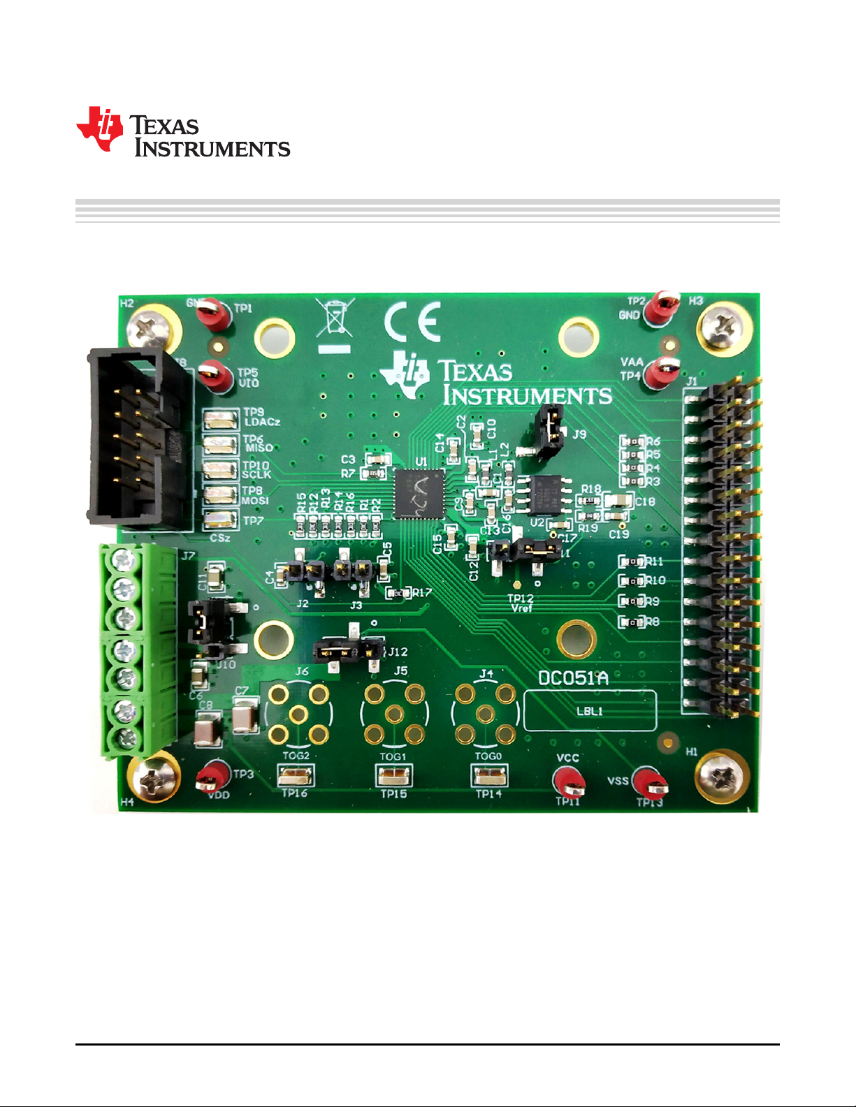
DAC81416EVM
This user's guide describes the characteristics, operation, and use of the DAC81416 evaluation module
(EVM). This document also discusses the proper setup and configuration of both software and hardware,
and reviews various aspects of program operation. Throughout this document, the terms evaluation board,
evaluation module, and EVM are synonymous with the DAC81416EVM. A complete circuit description,
schematic diagram, and bill of materials are also included in this document.
SLAU777A–June 2018–Revised December 2018
Submit Documentation Feedback
Copyright © 2018, Texas Instruments Incorporated
DAC81416EVM
1
Page 2

www.ti.com
Contents
1 Overview ..................................................................................................................... 3
2 System Setup ................................................................................................................ 4
3 Detailed Description ......................................................................................................... 6
4 Schematic, PCB Layout, and Bill of Materials.......................................................................... 12
List of Figures
1 DAC81416EVM Hardware Setup.......................................................................................... 4
2 Launching Software Setup ................................................................................................. 5
3 DAC81416EVM Installation Path .......................................................................................... 5
4 DAC81416EVM Hardware Block Diagram ............................................................................... 6
5 DAC Output Header......................................................................................................... 8
6 DAC81416EVM GUI Location.............................................................................................. 9
7 DAC81416EVM GUI Connection Detection.............................................................................. 9
8 DAC81416EVM Software Page Selection .............................................................................. 10
9 Low Level Configuration Page............................................................................................ 10
10 Low Level Configuration Page Options ................................................................................. 11
11 High Level Configuration Page........................................................................................... 11
12 DAC81416EVM Board Schematic ....................................................................................... 12
13 DAC81416EVM PCB Components Layout ............................................................................. 13
14 Top Layer ................................................................................................................... 14
15 Layer 2 - Ground Plane ................................................................................................... 15
16 Layer 3 - Power Plane..................................................................................................... 16
17 Bottom Layer................................................................................................................ 17
1 Contents of DAC81416EVM Kit............................................................................................ 3
2 Required Components Not Included in DAC81416EVM Kit ........................................................... 3
3 Related Documentation..................................................................................................... 3
4 Power Supply Inputs ........................................................................................................ 4
5 Jumper Settings.............................................................................................................. 6
6 J8 (USB2ANY) Pin Definitions............................................................................................. 7
7 J8 SPI Signal Test Points .................................................................................................. 7
8 J1 Pin Definitions ............................................................................................................ 8
9 DAC81416 EVM Bill of Materials......................................................................................... 18
Trademarks
Windows is a trademark of Microsoft Corporation.
All other trademarks are the property of their respective owners.
List of Tables
2
DAC81416EVM
Copyright © 2018, Texas Instruments Incorporated
SLAU777A–June 2018–Revised December 2018
Submit Documentation Feedback
Page 3
www.ti.com
1 Overview
The DAC81416EVM is an easy to use platform for evaluating the functionality and performance of the
DAC81416 device. The DAC81416 is a 16-channel, buffered, high-voltage output digital-to-analog
converter (DAC) in 16-bit resolution with 2.5-V internal reference. This EVM provides bipolar output
voltage up to ±20 V and unipolar up to 40 V. The EVM provides the SPI programming interface using a
PC-based graphical user interface (GUI).
1.1 Kit Contents
Table 1 details the contents of the EVM kit. Contact the TI Product Information Center nearest you if any
component is missing. Make sure to verify the latest versions of the related software at the TI website,
www.ti.com.
Overview
Table 1. Contents of DAC81416EVM Kit
Item Quantity
DAC81416EVM evaluation board PCB 1
Table 2. Required Components Not Included in
DAC81416EVM Kit
Item Quantity
USB2ANY interface adapter 1
1.2 Related Documentation from Texas Instruments
The following document provides information regarding Texas Instruments integrated circuits used in the
assembly of the DAC81416EVM. This user's guide is available from the TI web site under literature
number SLAU777. Any letter appended to the literature number corresponds to the document revision that
is current at the time of the writing of this document. Newer revisions may be available from the TI web
site at http://www.ti.com/, or call the Texas Instruments Literature Response Center at (800) 477-8924 or
the Product Information Center at (972) 644-5580. When ordering, identify the document by both title and
literature number.
Table 3. Related Documentation
Document Literature Number
DAC81416 product data sheet SLASEO0
SLAU777A–June 2018–Revised December 2018
Submit Documentation Feedback
Copyright © 2018, Texas Instruments Incorporated
DAC81416EVM
3
Page 4
USB2ANY
Power Supply
System Setup
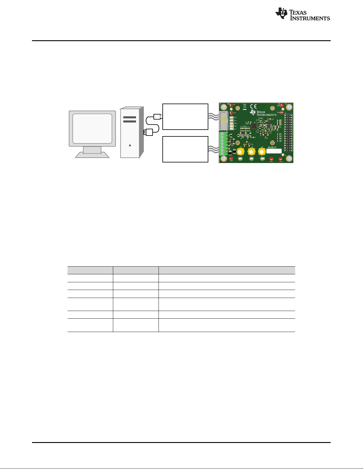
2 System Setup
2.1 Hardware Setup
This section provides the overall system setup for the EVM. Use a PC to run the software that provides an
interface to the USB2ANY platform. This platform generates the optional VIO power and digital signals
used to communicate with the EVM board. Test point connections are included on the EVM board for
external power supplies. Figure 1 displays the system setup for the DAC81416EVM.
Figure 1. DAC81416EVM Hardware Setup
2.1.1 Connecting the Hardware
Connect the USB cable from the USB2ANY platform to the PC. To connect the USB2ANY to the EVM
board, align and firmly connect the keyed ribbon connector to the J8 connector. Verify that the connection
is snug because loose connections may cause intermittent operation.
www.ti.com
2.1.2 Power Configurations
The DAC81416EVM provides electrical connections to the device supply pins. The connectors and
optional configurations are shown in the Table 4.
Table 4. Power Supply Inputs
Connector.Pin Supply Name Voltage Range
J7.3 GND 0 V
J7.4 VIO 1.7 V to 5.5 V
J7.5 VDD/VAA 4.5 V to 5.5 V
J7.6 VSS
J7.7 VCC 9 V to 41.5 V
J8.5 VIO
2.1.3 Electrostatic Discharge Warning
Many of the components on the DAC81416EVM are susceptible to damage by electrostatic discharge
(ESD). Observe proper ESD handling precautions when unpacking and handling the EVM, including the
use of a grounded wrist strap at an approved ESD workstation.
–21.5 V to 0 V
Note: 9 V < (VCC – VSS) < 43 V
1.7 V to 5.5 V
Note: J10 selects between J7.4 and J8.5
4
DAC81416EVM
Copyright © 2018, Texas Instruments Incorporated
SLAU777A–June 2018–Revised December 2018
Submit Documentation Feedback
Page 5
www.ti.com
2.2 Software Setup
This section provides the procedure for EVM software installation.
2.2.1 Operating Systems
The EVM software is compatible with the Windows™ 7, Windows 8, and Windows 10 operating systems.
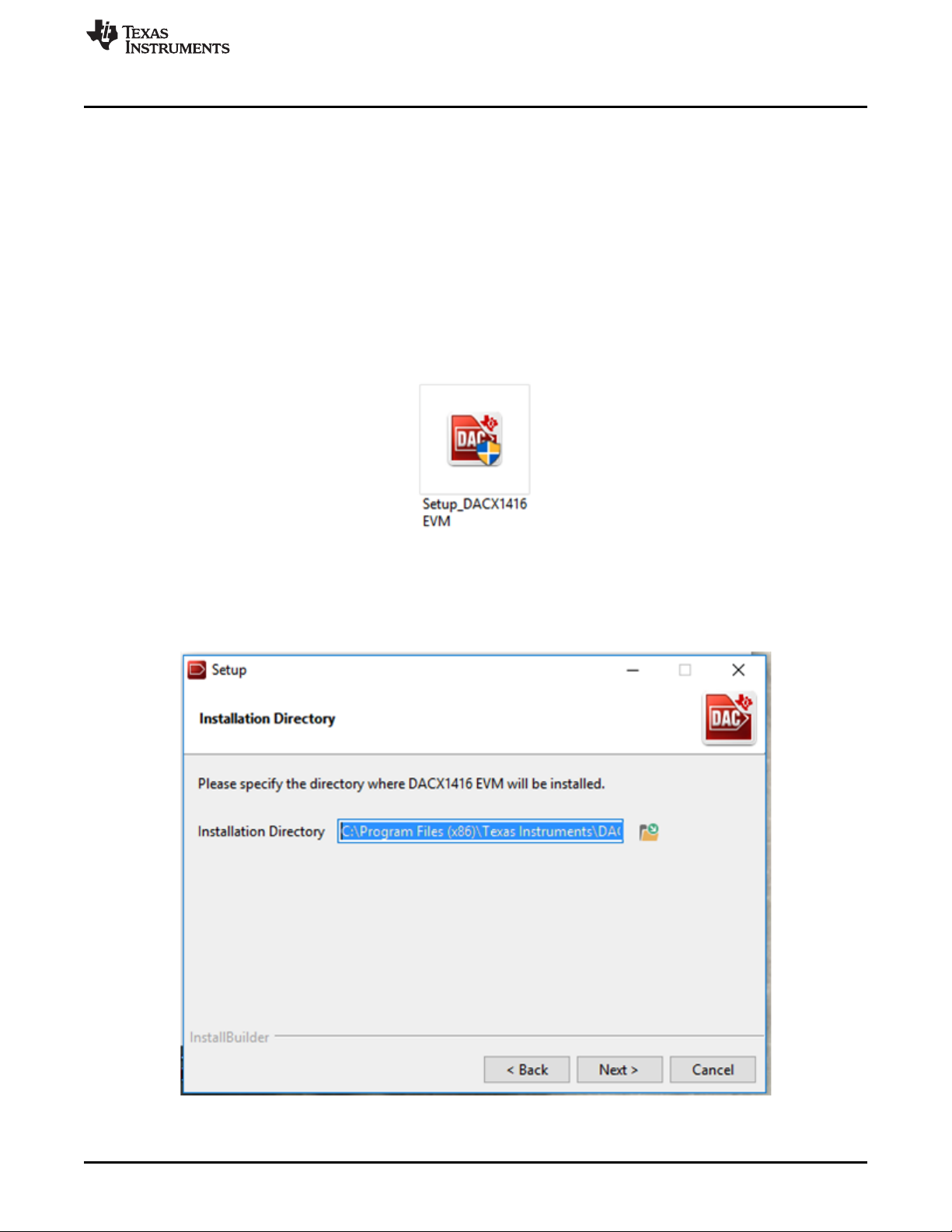
2.2.2 Software Installation
The software is available through the EVM product folder on the TI website. After the software is
downloaded to the PC, navigate to the DAC81416EVM folder, and run the Setup_DAC81416_EVM.exe
file, as shown in Figure 2. When the software is launched, an installation dialog window opens and
prompts the user to select an installation directory. If left unchanged, the software location defaults to
C:\Program Files (x86)\Texas Instruments\DAC81416 EVM as shown in Figure 3.
System Setup
Figure 2. Launching Software Setup
The software installation automatically copies the required LabVIEW files and drivers to the local machine.
Make sure to verify that the USB2ANY is not connected before the software installation, or the file and
driver installation may be affected.
Figure 3. DAC81416EVM Installation Path
SLAU777A–June 2018–Revised December 2018
Submit Documentation Feedback
Copyright © 2018, Texas Instruments Incorporated
DAC81416EVM
5
Page 6
DAC81416
USB2ANY
Connector
Power and
External
Reference
Input
Connector
Output
Connector
Onboard Jumper
Settings
Onboard
Reference
Detailed Description
3 Detailed Description
3.1 Hardware Description
The following sections provide detailed information on the EVM hardware and jumper configuration
settings. Table 5 displays the default configurations of all jumper connections on the DAC81416EVM.
Connect the USB cable from the USB2ANY to the PC.
Table 5. Jumper Settings
Jumper Default Position Available Option Description
J2 Open: RESET deactivated Closed: RESET activated RESET activation or deactivation
J3 Open: CLR deactivated Closed: CLR activated CLR activation or deactivation
J9 Closed: GND Open: external REFGND REFGND selection
J10 1-2: USB2ANY 3.3 V on J8.5 2-3: external VIO on J7.4 VIO selection
J11 1-2: VREF from REF5025 2-3: external VREF on J7.1
J12 2-3: VSS on J7.6 1-2: GND VSS selection
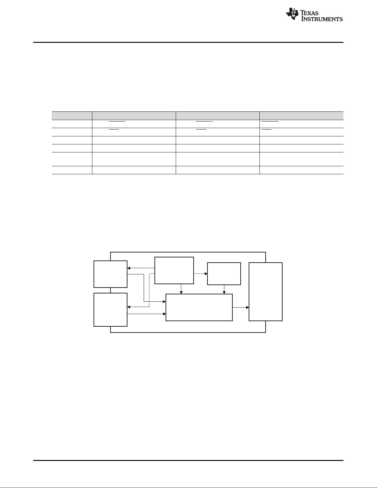
3.1.1 Theory of Operation for DAC81416 Hardware
The block diagram of the DAC81416EVM board is displayed in Figure 4. The EVM board connects to
external power supplies VCC, VSS, VDD/VAA and VIO through an external 7-pin terminal block. This
connector also provides an option for an external reference. The 32-pin header provides the 16 DAC
outputs and other signals, such as VREF, TEMPOUT and ALMOUT. The 10-pin wire-to-board connector
provides an interface to the USB2ANY platform. The SPI signals are provided either by using the
USB2ANY header or the test points. The USB2ANY also provides an optional 3.3-V VIO selectable by
jumper settings. There is also an onboard 2.5-V reference source.
www.ti.com
VREF selection note: deselect both
before selecting internal reference
Figure 4. DAC81416EVM Hardware Block Diagram
6
DAC81416EVM
Copyright © 2018, Texas Instruments Incorporated
SLAU777A–June 2018–Revised December 2018
Submit Documentation Feedback
Page 7
www.ti.com
3.1.2 Signal Definition of USB2ANY
The DAC81416EVM provides a hardware connector (J8) that connects to the USB2ANY interface board
The USBANY platform supplies VIO power and is responsible for providing the SPI commands sent from
the PC GUI software. Optionally, the VIO supply can be provided through an external supply, and all
digital communication lines can be accessed through their respective digital test points. Table 6 provides
the pin definitions for this connector. Table 7 provides the corresponding test points for the SPI signals.
Table 6. J8 (USB2ANY) Pin Definitions
Pin# Signal Description
1 GPIO7 General purpose I/O
2 CS/GPIO6 CS or general-purpose I/O
3 RXD/MISO SPI MISO
4 TXD/MOSI SPI MOSI
5 3.3V 3.3-V supply
6 GND Ground
7 GPIO3 General-purpose I/O
SCLK/GPIO2 SPI SCLK or general-purpose
8
9 GPIO1 General-purpose I/O
10 GPIO0 General-purpose I/O
Detailed Description
I/O
3.1.3 DAC Signal Pins
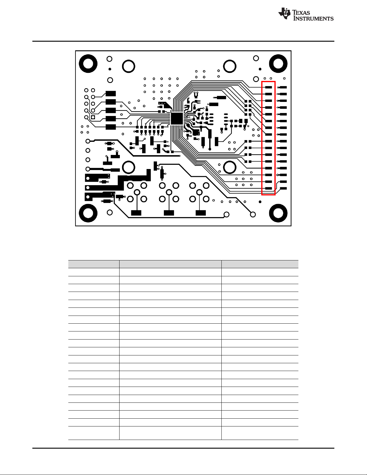
The DAC81416EVM provides access to all DAC outputs through connection J1, as shown in Figure 5, and
listed in Table 8.
Table 7. J8 SPI Signal Test Points
Test Points SPI Signal
TP6 MISO, SDO
TP7 CS
TP8 MOSI, SDI
TP9 LDAC
TP10 SCLK
SLAU777A–June 2018–Revised December 2018
Submit Documentation Feedback
Copyright © 2018, Texas Instruments Incorporated
DAC81416EVM
7
Page 8
Detailed Description
www.ti.com
Figure 5. DAC Output Header
Table 8. J1 Pin Definitions
Connector/Pin Supply Name Voltage Range
OUT0 J1.18 DAC output voltage
OUT1 J1.20 DAC output voltage
OUT2 J1.22 DAC output voltage
OUT3 J1.24 DAC output voltage
OUT4 J1.26 DAC output voltage
OUT5 J1.28 DAC output voltage
OUT6 J1.30 DAC output voltage
OUT7 J1.32 DAC output voltage
OUT8 J1.2 DAC output voltage
OUT9 J1.4 DAC output voltage
OUT10 J1.6 DAC output voltage
OUT11 J1.8 DAC output voltage
OUT12 J1.10 DAC output voltage
OUT13 J1.12 DAC output voltage
OUT15 J1.14 DAC output voltage
OUT16 J1.16 DAC output voltage
ALMOUT J1.1 DAC alarm output
TEMPOUT J1.3 DAC temperature output
REFGND J1.5 DAC REFGND
VREF J1.7 DAC reference
GND
J1.9, J1.11, J1.13, J1.15, J1.17, J1.19, J1.21,
J1.23, J1.25, J1.27, J1.29, J1.31
DAC ground
8
DAC81416EVM
Copyright © 2018, Texas Instruments Incorporated
SLAU777A–June 2018–Revised December 2018
Submit Documentation Feedback
Page 9

www.ti.com
3.2 Software Description
This section describes the features of the DAC81416 EVM software, and discusses how to use these
features. The software provides basic control of all the registers and functions to the DAC81416 device.
3.2.1 Starting the Software
After the DAC81416EVM software is installed, a restart may be required by Windows. To launch the
software, locate the Texas Instruments folder in the All Programs menu, and select the DACX1416 EVM
icon.
Detailed Description
Figure 6. DAC81416EVM GUI Location
Figure 7 shows that the USB2ANY is correctly connected because the status bar at the bottom of the
screen displays HARDWARE CONNECTED. If the USB2ANY is not properly connected or not connected
at all, the status bar displays DEMO. If the GUI is not displaying the HARDWARE CONNECTED status
while the USB2ANY is connected, unplug and reconnect the USB2ANY, and relaunch the GUI software.
Figure 7. DAC81416EVM GUI Connection Detection
SLAU777A–June 2018–Revised December 2018
Submit Documentation Feedback
Copyright © 2018, Texas Instruments Incorporated
DAC81416EVM
9
Page 10
Detailed Description
3.2.2 Software Features
The DAC81416 EVM incorporates interactive functions that help configure the DAC81416 device. These
functions are built into several GUI pages, as shown in Figure 8. Use the Page Selection menu to switch
between the pages, with each page representing a feature of the software.
Figure 8. DAC81416EVM Software Page Selection
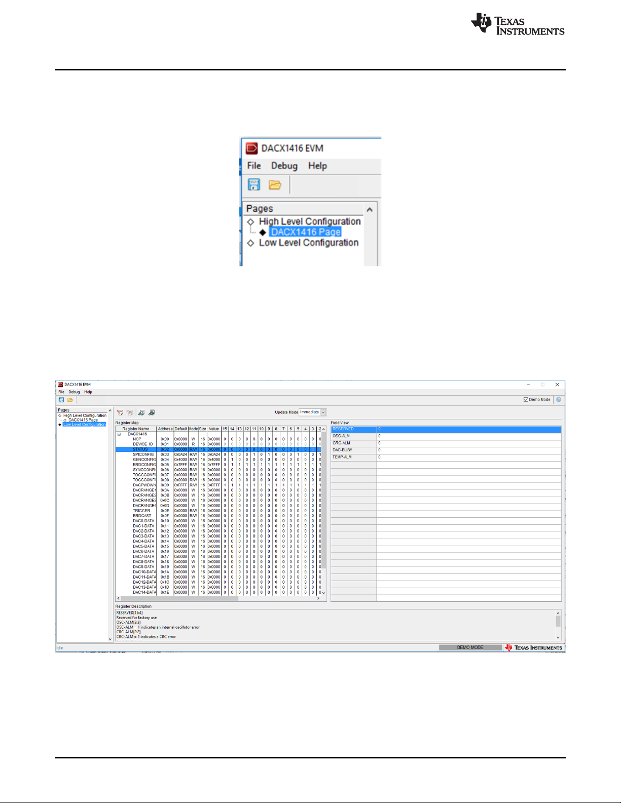
3.2.2.1 Low Level Configuration Page
The DAC81416 EVM Register Map page, shown in Figure 9, provides access to low-level communication
directly with the DAC81416 registers. Selecting a register on the Register Map list shows a description of
the values in that register, as well as information on the register address, default value, size, and current
value. Values can be read and written to the registers by writing to the Value or bit field of the GUI.
www.ti.com
10
DAC81416EVM
Figure 9. Low Level Configuration Page
SLAU777A–June 2018–Revised December 2018
Copyright © 2018, Texas Instruments Incorporated
Submit Documentation Feedback
Page 11

www.ti.com
The values of the register map can also be saved by pressing the Save Configuration button under the
File menu option. Additionally, the configuration files can be accessed through the Load Configuration
button. Other selectable options include the Update Mode, Write Selected, Read Selected, Write Modified,
and Read All buttons. All buttons are displayed in Figure 10.
Figure 10. Low Level Configuration Page Options
If Immediate is selected under Update Mode, all changes to register values update immediately. Use the
Deferred option to modify the value of a register without taking effect until the Write Selected, or Write
Modified button is pressed. The Read Selected button allows individual register reads, whereas the Read
All button reads the status of all registers located in the register map.
3.2.2.2 High Level Configuration Page
The High Level Configuration page provides an interface to monitor and control the different data
registers, modes, and configurations available for the DAC81416 device. This page is displayed in
Figure 11.
Detailed Description
Figure 11. High Level Configuration Page
Power Down: The power-down bits of all 16 DAC channels and the global power down bit are all enabled
by default. Both the device and individual channels must be powered up in order to get output.
Reference: The internal voltage reference is by default OFF on DACx1416. The EVM selects the onboard
reference by default.
Output Range: The DACx1416 provides various range options at individual channel level. This selection
can be done on the GUI.
DAC Outputs: The DAC outputs can be operated either in single-ended or differential modes.
SLAU777A–June 2018–Revised December 2018
Submit Documentation Feedback
Copyright © 2018, Texas Instruments Incorporated
DAC81416EVM
11
Page 12

Schematic, PCB Layout, and Bill of Materials
4 Schematic, PCB Layout, and Bill of Materials
This section contains the schematic diagram, printed circuit board layout, and a complete bill of materials
for the DAC81416EVM.
4.1 Board Schematic
www.ti.com
Figure 12. DAC81416EVM Board Schematic
12
DAC81416EVM
Copyright © 2018, Texas Instruments Incorporated
SLAU777A–June 2018–Revised December 2018
Submit Documentation Feedback
Page 13
www.ti.com
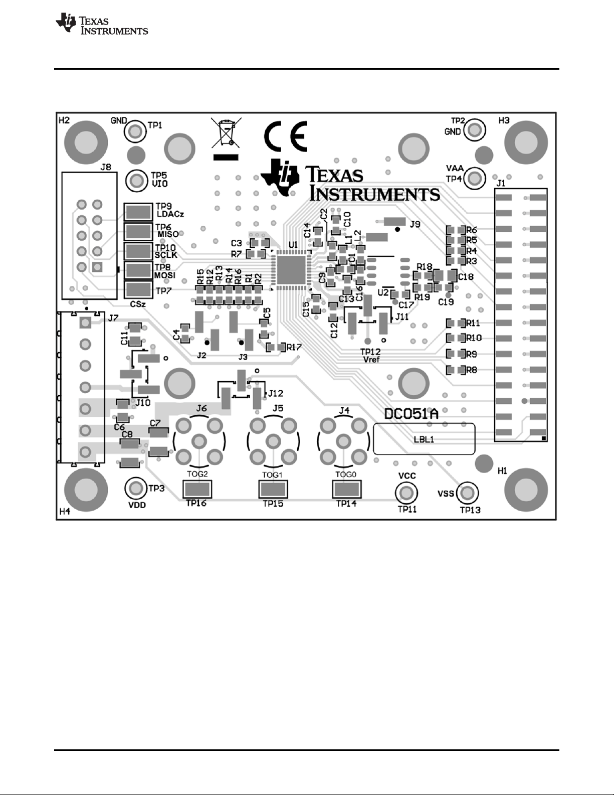
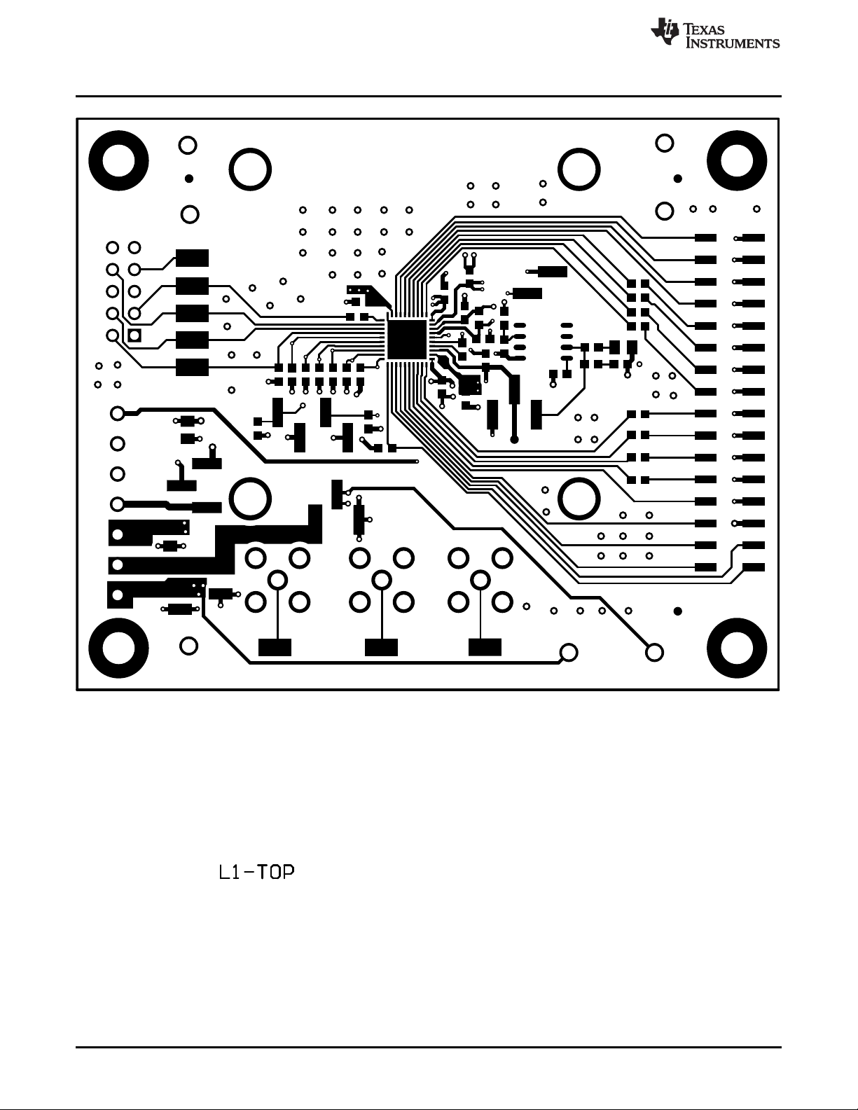
4.2 PCB Components Layout
Figure 13 through Figure 17 show the layout of the components for the DAC81416EVM board.
Schematic, PCB Layout, and Bill of Materials
Figure 13. DAC81416EVM PCB Components Layout
SLAU777A–June 2018–Revised December 2018
Submit Documentation Feedback
Copyright © 2018, Texas Instruments Incorporated
DAC81416EVM
13
Page 14
Schematic, PCB Layout, and Bill of Materials
www.ti.com
14
DAC81416EVM
Figure 14. Top Layer
Copyright © 2018, Texas Instruments Incorporated
SLAU777A–June 2018–Revised December 2018
Submit Documentation Feedback
Page 15

www.ti.com
Schematic, PCB Layout, and Bill of Materials
SLAU777A–June 2018–Revised December 2018
Submit Documentation Feedback
Figure 15. Layer 2 - Ground Plane
Copyright © 2018, Texas Instruments Incorporated
DAC81416EVM
15
Page 16

Schematic, PCB Layout, and Bill of Materials
www.ti.com
16
DAC81416EVM
Figure 16. Layer 3 - Power Plane
Copyright © 2018, Texas Instruments Incorporated
SLAU777A–June 2018–Revised December 2018
Submit Documentation Feedback
Page 17

www.ti.com
Schematic, PCB Layout, and Bill of Materials
SLAU777A–June 2018–Revised December 2018
Submit Documentation Feedback
Figure 17. Bottom Layer
Copyright © 2018, Texas Instruments Incorporated
DAC81416EVM
17
Page 18

Schematic, PCB Layout, and Bill of Materials
4.3 Bill of Materials
Table 9 lists the bill of materials (BOM).
Table 9. DAC81416 EVM Bill of Materials
Designator Quantity Value Description Package Reference Part Number Manufacturer
!PCB 1 Printed Circuit Board DC051 Any
@H1, @H2, @H3, @H4 4 Hex Standoff, #4-40,
C1, C4, C5, C10, C12,
C14, C15
C2, C3, C13 3 0.1uF CAP, CERM, 0.1 uF, 16
C6, C11, C18 3 10uF CAP, CERM, 10 uF, 35
C7, C8 2 10uF CAP, CERM, 10 uF, 50
C9 1 1000pF CAP, CERM, 1000 pF,
C16, C17, C19 3 1uF CAP, CERM, 1 uF, 25 V,
H1, H2, H3, H4 4 Screw Pan Head M3 Screw M3 29311 Keystone
J1 1 Header, 100mil, 16x2,
J2, J3, J9 3 Header, 100mil, 2x1,
J7 1 TERM BLOCK, 7POS,
J8 1 Header(Shrouded),
J10, J11, J12 3 Header, 2.54mm, 3x1,
L1, L2 2 600 ohm Ferrite Bead, 600 ohm @
LBL1 1 Thermal Transfer
R1, R2, R12, R13, R14,
R15, R16, R17
7 1uF CAP, CERM, 1 uF, 16 V,
8 10.0k RES, 10.0 k, 1%, 0.1 W,
Aluminum, 1/4"
+/- 10%, X5R, 0603
V, +/- 5%, X7R, 0603
V, +/- 10%, X6S, 0805
V, +/- 10%, X7R, AECQ200 Grade 1, 1210
50 V, +/- 10%, X7R,
0603
+/- 10%, X5R, 0603
Tin, SMT
Gold with Tin Tail, SMT
3.5MM, TH
2.54mm, 5x2, Gold, TH
Gold, SMT
100 MHz, 1 A, 0603
Printable Labels, 0.650"
W x 0.200" H - 10,000
per roll
0603
1/4 inch Aluminum Hex
Standoff
0603 C0603C105K4PACTU Kemet
0603 C0603C104J4RACTU Kemet
0805 GRM21BC8YA106KE11L MuRata
1210 UMJ325KB7106KMHT Taiyo Yuden
0603 C0603C102K5RACTU Kemet
0603 C1608X5R1E105K080ACTDK
16x2 Header TSM-116-01-T-DV-P Samtec
2x1 Header TSM-102-01-L-SV Samtec
24.5x9.2x7.6mm 1984662 Phoenix Contact
Header, 2.54mm, 5x2,THAWHW-10G-0202-T Assman WSW
Header, 2.54mm, 3x1,
SMT
0603 742792651 Wurth Elektronik
PCB Label 0.650 x 0.200
inch
0603 RC0603FR-0710KL Yageo America
1891 Keystone
TSM-103-01-L-SV-P-TR Samtec
THT-14-423-10 Brady
www.ti.com
18
DAC81416EVM
SLAU777A–June 2018–Revised December 2018
Submit Documentation Feedback
Copyright © 2018, Texas Instruments Incorporated
Page 19

www.ti.com
Schematic, PCB Layout, and Bill of Materials
Table 9. DAC81416 EVM Bill of Materials (continued)
Designator Quantity Value Description Package Reference Part Number Manufacturer
R3, R4, R5, R6, R8, R9,
R10, R11
R7 1 33 RES, 33, 5%, 0.1 W,
R18 1 0.51 RES, 0.51, 1%, 0.1 W,
R19 1 1.00 RES, 1.00, 1%, 0.1 W,
SH-J1, SH-J2, SH-J3,
SH-J4
TP1, TP2, TP3, TP4,
TP5, TP11, TP13
TP6, TP7, TP8, TP9,
TP10, TP14, TP15, TP16
U1 1 16-Channel, 16-Bit, High-
U2 1 Low Noise, Very Low
H5 0 Square Basket Heatsink
J4, J5, J6 0 Connector, SMA, TH SMA 142-0701-231 Cinch Connectivity
8 0 RES, 0, 5%, 0.1 W, 0603 0603 RC0603JR-070RL Yageo America
AEC-Q200 Grade 0,
0603
AEC-Q200 Grade 1,
0603
0603
4 1x2 Shunt, 100mil, Gold
plated, Black
7 Test Point, Compact,
Red, TH
8 Test Point, Miniature,
SMT
Voltage Output DAC with
Precision Internal
Reference, RHA0040H
(VQFN-40)
Drift, Precision Voltage
Reference, -40 to 125
degC, 8-pin SOIC (D),
Green (RoHS & no
Sb/Br)
Featuring Slanted Fins
0603 CRCW060333R0JNEA Vishay-Dale
0603 ERJ-3RQFR51V Panasonic
0603 RC0603FR-071RL Yageo America
Shunt SNT-100-BK-G Samtec
Red Compact Testpoint 5005 Keystone
Test Point, Miniature,
SMT
RHA0040H DAC81416RHA Texas Instruments
D0008A REF5025AIDR Texas Instruments
Heat Sink TO-3 500403B00000G Aavid
5019 Keystone
SLAU777A–June 2018–Revised December 2018
Submit Documentation Feedback
Copyright © 2018, Texas Instruments Incorporated
DAC81416EVM
19
Page 20

Revision History
www.ti.com
Revision History
Changes from Original (June 2018) to A Revision ......................................................................................................... Page
• Deleted USB2ANY adapter from Table 1.............................................................................................. 3
• Added new Table 2 ....................................................................................................................... 3
• Changed contents of Table 4............................................................................................................ 4
• Changed connector.pin numbers in Table 5 to match the connector.pin numbers listed in Table 4........................... 6
• Changed connector numbers in Table 8; updated for clarity ........................................................................ 8
20
Revision History
Copyright © 2018, Texas Instruments Incorporated
SLAU777A–June 2018–Revised December 2018
Submit Documentation Feedback
Page 21

STANDARD TERMS FOR EVALUATION MODULES
1. Delivery: TI delivers TI evaluation boards, kits, or modules, including any accompanying demonstration software, components, and/or
documentation which may be provided together or separately (collectively, an “EVM” or “EVMs”) to the User (“User”) in accordance
with the terms set forth herein. User's acceptance of the EVM is expressly subject to the following terms.
1.1 EVMs are intended solely for product or software developers for use in a research and development setting to facilitate feasibility
evaluation, experimentation, or scientific analysis of TI semiconductors products. EVMs have no direct function and are not
finished products. EVMs shall not be directly or indirectly assembled as a part or subassembly in any finished product. For
clarification, any software or software tools provided with the EVM (“Software”) shall not be subject to the terms and conditions
set forth herein but rather shall be subject to the applicable terms that accompany such Software
1.2 EVMs are not intended for consumer or household use. EVMs may not be sold, sublicensed, leased, rented, loaned, assigned,
or otherwise distributed for commercial purposes by Users, in whole or in part, or used in any finished product or production
system.
2 Limited Warranty and Related Remedies/Disclaimers:
2.1 These terms do not apply to Software. The warranty, if any, for Software is covered in the applicable Software License
Agreement.
2.2 TI warrants that the TI EVM will conform to TI's published specifications for ninety (90) days after the date TI delivers such EVM
to User. Notwithstanding the foregoing, TI shall not be liable for a nonconforming EVM if (a) the nonconformity was caused by
neglect, misuse or mistreatment by an entity other than TI, including improper installation or testing, or for any EVMs that have
been altered or modified in any way by an entity other than TI, (b) the nonconformity resulted from User's design, specifications
or instructions for such EVMs or improper system design, or (c) User has not paid on time. Testing and other quality control
techniques are used to the extent TI deems necessary. TI does not test all parameters of each EVM.
User's claims against TI under this Section 2 are void if User fails to notify TI of any apparent defects in the EVMs within ten (10)
business days after delivery, or of any hidden defects with ten (10) business days after the defect has been detected.
2.3 TI's sole liability shall be at its option to repair or replace EVMs that fail to conform to the warranty set forth above, or credit
User's account for such EVM. TI's liability under this warranty shall be limited to EVMs that are returned during the warranty
period to the address designated by TI and that are determined by TI not to conform to such warranty. If TI elects to repair or
replace such EVM, TI shall have a reasonable time to repair such EVM or provide replacements. Repaired EVMs shall be
warranted for the remainder of the original warranty period. Replaced EVMs shall be warranted for a new full ninety (90) day
warranty period.
3 Regulatory Notices:
3.1 United States
3.1.1 Notice applicable to EVMs not FCC-Approved:
FCC NOTICE: This kit is designed to allow product developers to evaluate electronic components, circuitry, or software
associated with the kit to determine whether to incorporate such items in a finished product and software developers to write
software applications for use with the end product. This kit is not a finished product and when assembled may not be resold or
otherwise marketed unless all required FCC equipment authorizations are first obtained. Operation is subject to the condition
that this product not cause harmful interference to licensed radio stations and that this product accept harmful interference.
Unless the assembled kit is designed to operate under part 15, part 18 or part 95 of this chapter, the operator of the kit must
operate under the authority of an FCC license holder or must secure an experimental authorization under part 5 of this chapter.
3.1.2 For EVMs annotated as FCC – FEDERAL COMMUNICATIONS COMMISSION Part 15 Compliant:
CAUTION
This device complies with part 15 of the FCC Rules. Operation is subject to the following two conditions: (1) This device may not
cause harmful interference, and (2) this device must accept any interference received, including interference that may cause
undesired operation.
Changes or modifications not expressly approved by the party responsible for compliance could void the user's authority to
operate the equipment.
FCC Interference Statement for Class A EVM devices
NOTE: This equipment has been tested and found to comply with the limits for a Class A digital device, pursuant to part 15 of
the FCC Rules. These limits are designed to provide reasonable protection against harmful interference when the equipment is
operated in a commercial environment. This equipment generates, uses, and can radiate radio frequency energy and, if not
installed and used in accordance with the instruction manual, may cause harmful interference to radio communications.
Operation of this equipment in a residential area is likely to cause harmful interference in which case the user will be required to
correct the interference at his own expense.
Page 22

FCC Interference Statement for Class B EVM devices
NOTE: This equipment has been tested and found to comply with the limits for a Class B digital device, pursuant to part 15 of
the FCC Rules. These limits are designed to provide reasonable protection against harmful interference in a residential
installation. This equipment generates, uses and can radiate radio frequency energy and, if not installed and used in accordance
with the instructions, may cause harmful interference to radio communications. However, there is no guarantee that interference
will not occur in a particular installation. If this equipment does cause harmful interference to radio or television reception, which
can be determined by turning the equipment off and on, the user is encouraged to try to correct the interference by one or more
of the following measures:
• Reorient or relocate the receiving antenna.
• Increase the separation between the equipment and receiver.
• Connect the equipment into an outlet on a circuit different from that to which the receiver is connected.
• Consult the dealer or an experienced radio/TV technician for help.
3.2 Canada
3.2.1 For EVMs issued with an Industry Canada Certificate of Conformance to RSS-210 or RSS-247
Concerning EVMs Including Radio Transmitters:
This device complies with Industry Canada license-exempt RSSs. Operation is subject to the following two conditions:
(1) this device may not cause interference, and (2) this device must accept any interference, including interference that may
cause undesired operation of the device.
Concernant les EVMs avec appareils radio:
Le présent appareil est conforme aux CNR d'Industrie Canada applicables aux appareils radio exempts de licence. L'exploitation
est autorisée aux deux conditions suivantes: (1) l'appareil ne doit pas produire de brouillage, et (2) l'utilisateur de l'appareil doit
accepter tout brouillage radioélectrique subi, même si le brouillage est susceptible d'en compromettre le fonctionnement.
Concerning EVMs Including Detachable Antennas:
Under Industry Canada regulations, this radio transmitter may only operate using an antenna of a type and maximum (or lesser)
gain approved for the transmitter by Industry Canada. To reduce potential radio interference to other users, the antenna type
and its gain should be so chosen that the equivalent isotropically radiated power (e.i.r.p.) is not more than that necessary for
successful communication. This radio transmitter has been approved by Industry Canada to operate with the antenna types
listed in the user guide with the maximum permissible gain and required antenna impedance for each antenna type indicated.
Antenna types not included in this list, having a gain greater than the maximum gain indicated for that type, are strictly prohibited
for use with this device.
Concernant les EVMs avec antennes détachables
Conformément à la réglementation d'Industrie Canada, le présent émetteur radio peut fonctionner avec une antenne d'un type et
d'un gain maximal (ou inférieur) approuvé pour l'émetteur par Industrie Canada. Dans le but de réduire les risques de brouillage
radioélectrique à l'intention des autres utilisateurs, il faut choisir le type d'antenne et son gain de sorte que la puissance isotrope
rayonnée équivalente (p.i.r.e.) ne dépasse pas l'intensité nécessaire à l'établissement d'une communication satisfaisante. Le
présent émetteur radio a été approuvé par Industrie Canada pour fonctionner avec les types d'antenne énumérés dans le
manuel d’usage et ayant un gain admissible maximal et l'impédance requise pour chaque type d'antenne. Les types d'antenne
non inclus dans cette liste, ou dont le gain est supérieur au gain maximal indiqué, sont strictement interdits pour l'exploitation de
l'émetteur
3.3 Japan
3.3.1 Notice for EVMs delivered in Japan: Please see http://www.tij.co.jp/lsds/ti_ja/general/eStore/notice_01.page 日本国内に
輸入される評価用キット、ボードについては、次のところをご覧ください。
http://www.tij.co.jp/lsds/ti_ja/general/eStore/notice_01.page
3.3.2 Notice for Users of EVMs Considered “Radio Frequency Products” in Japan: EVMs entering Japan may not be certified
by TI as conforming to Technical Regulations of Radio Law of Japan.
If User uses EVMs in Japan, not certified to Technical Regulations of Radio Law of Japan, User is required to follow the
instructions set forth by Radio Law of Japan, which includes, but is not limited to, the instructions below with respect to EVMs
(which for the avoidance of doubt are stated strictly for convenience and should be verified by User):
1. Use EVMs in a shielded room or any other test facility as defined in the notification #173 issued by Ministry of Internal
Affairs and Communications on March 28, 2006, based on Sub-section 1.1 of Article 6 of the Ministry’s Rule for
Enforcement of Radio Law of Japan,
2. Use EVMs only after User obtains the license of Test Radio Station as provided in Radio Law of Japan with respect to
EVMs, or
3. Use of EVMs only after User obtains the Technical Regulations Conformity Certification as provided in Radio Law of Japan
with respect to EVMs. Also, do not transfer EVMs, unless User gives the same notice above to the transferee. Please note
that if User does not follow the instructions above, User will be subject to penalties of Radio Law of Japan.
Page 23

【無線電波を送信する製品の開発キットをお使いになる際の注意事項】 開発キットの中には技術基準適合証明を受けて
いないものがあります。 技術適合証明を受けていないもののご使用に際しては、電波法遵守のため、以下のいずれかの
措置を取っていただく必要がありますのでご注意ください。
1. 電波法施行規則第6条第1項第1号に基づく平成18年3月28日総務省告示第173号で定められた電波暗室等の試験設備でご使用
いただく。
2. 実験局の免許を取得後ご使用いただく。
3. 技術基準適合証明を取得後ご使用いただく。
なお、本製品は、上記の「ご使用にあたっての注意」を譲渡先、移転先に通知しない限り、譲渡、移転できないものとします。
上記を遵守頂けない場合は、電波法の罰則が適用される可能性があることをご留意ください。 日本テキサス・イ
ンスツルメンツ株式会社
東京都新宿区西新宿6丁目24番1号
西新宿三井ビル
3.3.3 Notice for EVMs for Power Line Communication: Please see http://www.tij.co.jp/lsds/ti_ja/general/eStore/notice_02.page
電力線搬送波通信についての開発キットをお使いになる際の注意事項については、次のところをご覧ください。http:/
/www.tij.co.jp/lsds/ti_ja/general/eStore/notice_02.page
3.4 European Union
3.4.1 For EVMs subject to EU Directive 2014/30/EU (Electromagnetic Compatibility Directive):
This is a class A product intended for use in environments other than domestic environments that are connected to a
low-voltage power-supply network that supplies buildings used for domestic purposes. In a domestic environment this
product may cause radio interference in which case the user may be required to take adequate measures.
4 EVM Use Restrictions and Warnings:
4.1 EVMS ARE NOT FOR USE IN FUNCTIONAL SAFETY AND/OR SAFETY CRITICAL EVALUATIONS, INCLUDING BUT NOT
LIMITED TO EVALUATIONS OF LIFE SUPPORT APPLICATIONS.
4.2 User must read and apply the user guide and other available documentation provided by TI regarding the EVM prior to handling
or using the EVM, including without limitation any warning or restriction notices. The notices contain important safety information
related to, for example, temperatures and voltages.
4.3 Safety-Related Warnings and Restrictions:
4.3.1 User shall operate the EVM within TI’s recommended specifications and environmental considerations stated in the user
guide, other available documentation provided by TI, and any other applicable requirements and employ reasonable and
customary safeguards. Exceeding the specified performance ratings and specifications (including but not limited to input
and output voltage, current, power, and environmental ranges) for the EVM may cause personal injury or death, or
property damage. If there are questions concerning performance ratings and specifications, User should contact a TI
field representative prior to connecting interface electronics including input power and intended loads. Any loads applied
outside of the specified output range may also result in unintended and/or inaccurate operation and/or possible
permanent damage to the EVM and/or interface electronics. Please consult the EVM user guide prior to connecting any
load to the EVM output. If there is uncertainty as to the load specification, please contact a TI field representative.
During normal operation, even with the inputs and outputs kept within the specified allowable ranges, some circuit
components may have elevated case temperatures. These components include but are not limited to linear regulators,
switching transistors, pass transistors, current sense resistors, and heat sinks, which can be identified using the
information in the associated documentation. When working with the EVM, please be aware that the EVM may become
very warm.
4.3.2 EVMs are intended solely for use by technically qualified, professional electronics experts who are familiar with the
dangers and application risks associated with handling electrical mechanical components, systems, and subsystems.
User assumes all responsibility and liability for proper and safe handling and use of the EVM by User or its employees,
affiliates, contractors or designees. User assumes all responsibility and liability to ensure that any interfaces (electronic
and/or mechanical) between the EVM and any human body are designed with suitable isolation and means to safely
limit accessible leakage currents to minimize the risk of electrical shock hazard. User assumes all responsibility and
liability for any improper or unsafe handling or use of the EVM by User or its employees, affiliates, contractors or
designees.
4.4 User assumes all responsibility and liability to determine whether the EVM is subject to any applicable international, federal,
state, or local laws and regulations related to User’s handling and use of the EVM and, if applicable, User assumes all
responsibility and liability for compliance in all respects with such laws and regulations. User assumes all responsibility and
liability for proper disposal and recycling of the EVM consistent with all applicable international, federal, state, and local
requirements.
5. Accuracy of Information: To the extent TI provides information on the availability and function of EVMs, TI attempts to be as accurate
as possible. However, TI does not warrant the accuracy of EVM descriptions, EVM availability or other information on its websites as
accurate, complete, reliable, current, or error-free.
Page 24

6. Disclaimers:
6.1 EXCEPT AS SET FORTH ABOVE, EVMS AND ANY MATERIALS PROVIDED WITH THE EVM (INCLUDING, BUT NOT
LIMITED TO, REFERENCE DESIGNS AND THE DESIGN OF THE EVM ITSELF) ARE PROVIDED "AS IS" AND "WITH ALL
FAULTS." TI DISCLAIMS ALL OTHER WARRANTIES, EXPRESS OR IMPLIED, REGARDING SUCH ITEMS, INCLUDING BUT
NOT LIMITED TO ANY EPIDEMIC FAILURE WARRANTY OR IMPLIED WARRANTIES OF MERCHANTABILITY OR FITNESS
FOR A PARTICULAR PURPOSE OR NON-INFRINGEMENT OF ANY THIRD PARTY PATENTS, COPYRIGHTS, TRADE
SECRETS OR OTHER INTELLECTUAL PROPERTY RIGHTS.
6.2 EXCEPT FOR THE LIMITED RIGHT TO USE THE EVM SET FORTH HEREIN, NOTHING IN THESE TERMS SHALL BE
CONSTRUED AS GRANTING OR CONFERRING ANY RIGHTS BY LICENSE, PATENT, OR ANY OTHER INDUSTRIAL OR
INTELLECTUAL PROPERTY RIGHT OF TI, ITS SUPPLIERS/LICENSORS OR ANY OTHER THIRD PARTY, TO USE THE
EVM IN ANY FINISHED END-USER OR READY-TO-USE FINAL PRODUCT, OR FOR ANY INVENTION, DISCOVERY OR
IMPROVEMENT, REGARDLESS OF WHEN MADE, CONCEIVED OR ACQUIRED.
7. USER'S INDEMNITY OBLIGATIONS AND REPRESENTATIONS. USER WILL DEFEND, INDEMNIFY AND HOLD TI, ITS
LICENSORS AND THEIR REPRESENTATIVES HARMLESS FROM AND AGAINST ANY AND ALL CLAIMS, DAMAGES, LOSSES,
EXPENSES, COSTS AND LIABILITIES (COLLECTIVELY, "CLAIMS") ARISING OUT OF OR IN CONNECTION WITH ANY
HANDLING OR USE OF THE EVM THAT IS NOT IN ACCORDANCE WITH THESE TERMS. THIS OBLIGATION SHALL APPLY
WHETHER CLAIMS ARISE UNDER STATUTE, REGULATION, OR THE LAW OF TORT, CONTRACT OR ANY OTHER LEGAL
THEORY, AND EVEN IF THE EVM FAILS TO PERFORM AS DESCRIBED OR EXPECTED.
8. Limitations on Damages and Liability:
8.1 General Limitations. IN NO EVENT SHALL TI BE LIABLE FOR ANY SPECIAL, COLLATERAL, INDIRECT, PUNITIVE,
INCIDENTAL, CONSEQUENTIAL, OR EXEMPLARY DAMAGES IN CONNECTION WITH OR ARISING OUT OF THESE
TERMS OR THE USE OF THE EVMS , REGARDLESS OF WHETHER TI HAS BEEN ADVISED OF THE POSSIBILITY OF
SUCH DAMAGES. EXCLUDED DAMAGES INCLUDE, BUT ARE NOT LIMITED TO, COST OF REMOVAL OR
REINSTALLATION, ANCILLARY COSTS TO THE PROCUREMENT OF SUBSTITUTE GOODS OR SERVICES, RETESTING,
OUTSIDE COMPUTER TIME, LABOR COSTS, LOSS OF GOODWILL, LOSS OF PROFITS, LOSS OF SAVINGS, LOSS OF
USE, LOSS OF DATA, OR BUSINESS INTERRUPTION. NO CLAIM, SUIT OR ACTION SHALL BE BROUGHT AGAINST TI
MORE THAN TWELVE (12) MONTHS AFTER THE EVENT THAT GAVE RISE TO THE CAUSE OF ACTION HAS
OCCURRED.
8.2 Specific Limitations. IN NO EVENT SHALL TI'S AGGREGATE LIABILITY FROM ANY USE OF AN EVM PROVIDED
HEREUNDER, INCLUDING FROM ANY WARRANTY, INDEMITY OR OTHER OBLIGATION ARISING OUT OF OR IN
CONNECTION WITH THESE TERMS, , EXCEED THE TOTAL AMOUNT PAID TO TI BY USER FOR THE PARTICULAR
EVM(S) AT ISSUE DURING THE PRIOR TWELVE (12) MONTHS WITH RESPECT TO WHICH LOSSES OR DAMAGES ARE
CLAIMED. THE EXISTENCE OF MORE THAN ONE CLAIM SHALL NOT ENLARGE OR EXTEND THIS LIMIT.
9. Return Policy. Except as otherwise provided, TI does not offer any refunds, returns, or exchanges. Furthermore, no return of EVM(s)
will be accepted if the package has been opened and no return of the EVM(s) will be accepted if they are damaged or otherwise not in
a resalable condition. If User feels it has been incorrectly charged for the EVM(s) it ordered or that delivery violates the applicable
order, User should contact TI. All refunds will be made in full within thirty (30) working days from the return of the components(s),
excluding any postage or packaging costs.
10. Governing Law: These terms and conditions shall be governed by and interpreted in accordance with the laws of the State of Texas,
without reference to conflict-of-laws principles. User agrees that non-exclusive jurisdiction for any dispute arising out of or relating to
these terms and conditions lies within courts located in the State of Texas and consents to venue in Dallas County, Texas.
Notwithstanding the foregoing, any judgment may be enforced in any United States or foreign court, and TI may seek injunctive relief
in any United States or foreign court.
Mailing Address: Texas Instruments, Post Office Box 655303, Dallas, Texas 75265
Copyright © 2018, Texas Instruments Incorporated
Page 25

IMPORTANT NOTICE AND DISCLAIMER
TI PROVIDES TECHNICAL AND RELIABILITY DATA (INCLUDING DATASHEETS), DESIGN RESOURCES (INCLUDING REFERENCE
DESIGNS), APPLICATION OR OTHER DESIGN ADVICE, WEB TOOLS, SAFETY INFORMATION, AND OTHER RESOURCES “AS IS”
AND WITH ALL FAULTS, AND DISCLAIMS ALL WARRANTIES, EXPRESS AND IMPLIED, INCLUDING WITHOUT LIMITATION ANY
IMPLIED WARRANTIES OF MERCHANTABILITY, FITNESS FOR A PARTICULAR PURPOSE OR NON-INFRINGEMENT OF THIRD
PARTY INTELLECTUAL PROPERTY RIGHTS.
These resources are intended for skilled developers designing with TI products. You are solely responsible for (1) selecting the appropriate
TI products for your application, (2) designing, validating and testing your application, and (3) ensuring your application meets applicable
standards, and any other safety, security, or other requirements. These resources are subject to change without notice. TI grants you
permission to use these resources only for development of an application that uses the TI products described in the resource. Other
reproduction and display of these resources is prohibited. No license is granted to any other TI intellectual property right or to any third
party intellectual property right. TI disclaims responsibility for, and you will fully indemnify TI and its representatives against, any claims,
damages, costs, losses, and liabilities arising out of your use of these resources.
TI’s products are provided subject to TI’s Terms of Sale (www.ti.com/legal/termsofsale.html) or other applicable terms available either on
ti.com or provided in conjunction with such TI products. TI’s provision of these resources does not expand or otherwise alter TI’s applicable
warranties or warranty disclaimers for TI products.
Mailing Address: Texas Instruments, Post Office Box 655303, Dallas, Texas 75265
Copyright © 2018, Texas Instruments Incorporated
 Loading...