

Page 1

DAC5674 EVM
User’ s Gu ide
September 2003 Wireless Infrastructure Products
SWRU007
Page 2

IMPORTANT NOTICE
Texas Instruments Incorporated and its subsidiaries (TI) reserve the right to make corrections, modifications,
enhancements, improvements, and other changes to its products and services at any time and to discontinue
any product or service without notice. Customers should obtain the latest relevant information before placing
orders and should verify that such information is current and complete. All products are sold subject to TI’s terms
and conditions of sale supplied at the time of order acknowledgment.
TI warrants performance of its hardware products to the specifications applicable at the time of sale in
accordance with TI’s standard warranty. Testing and other quality control techniques are used to the extent TI
deems necessary to support this warranty . Except where mandated by government requirements, testing of all
parameters of each product is not necessarily performed.
TI assumes no liability for applications assistance or customer product design. Customers are responsible for
their products and applications using TI components. To minimize the risks associated with customer products
and applications, customers should provide adequate design and operating safeguards.
TI does not warrant or represent that any license, either express or implied, is granted under any TI patent right,
copyright, mask work right, or other TI intellectual property right relating to any combination, machine, or process
in which TI products or services are used. Information published by TI regarding third-party products or services
does not constitute a license from TI to use such products or services or a warranty or endorsement thereof.
Use of such information may require a license from a third party under the patents or other intellectual property
of the third party, or a license from TI under the patents or other intellectual property of TI.
Reproduction of information in TI data books or data sheets is permissible only if reproduction is without
alteration and is accompanied by all associated warranties, conditions, limitations, and notices. Reproduction
of this information with alteration is an unfair and deceptive business practice. TI is not responsible or liable for
such altered documentation.
Resale of TI products or services with statements different from or beyond the parameters stated by TI for that
product or service voids all express and any implied warranties for the associated TI product or service and
is an unfair and deceptive business practice. TI is not responsible or liable for any such statements.
Following are URLs where you can obtain information on other Texas Instruments products and application
solutions:
Products Applications
Amplifiers amplifier.ti.com Audio www.ti.com/audio
Data Converters dataconverter.ti.com Automotive www.ti.com/automotive
DSP dsp.ti.com Broadband www.ti.com/broadband
Interface interface.ti.com Digital Control www.ti.com/digitalcontrol
Logic logic.ti.com Military www.ti.com/military
Power Mgmt power.ti.com Optical Networking www.ti.com/opticalnetwork
Microcontrollers microcontroller.ti.com Security www.ti.com/security
Telephony www.ti.com/telephony
Video & Imaging www.ti.com/video
Wireless www.ti.com/wireless
Mailing Address: Texas Instruments
Post Office Box 655303 Dallas, Texas 75265
Copyright 2003, Texas Instruments Incorporated
Page 3

EVM IMPORTANT NOTICE
Texas Instruments (TI) provides the enclosed product(s) under the following conditions:
This evaluation kit being sold by TI is intended for use for ENGINEERING DEVELOPMENT OR EVALUATION
PURPOSES ONLY and is not considered by TI to be fit for commercial use. As such, the goods being provided
may not be complete in terms of required design-, marketing-, and/or manufacturing-related protective
considerations, including product safety measures typically found in the end product incorporating the goods.
As a prototype, this product does not fall within the scope of the European Union directive on electromagnetic
compatibility and therefore may not meet the technical requirements of the directive.
Should this evaluation kit not meet the specifications indicated in the EVM User’s Guide, the kit may be returned
within 30 days from the date of delivery for a full refund. THE FOREGOING WARRANTY IS THE EXCLUSIVE
WARRANTY MADE BY SELLER TO BUYER AND IS IN LIEU OF ALL OTHER WARRANTIES, EXPRESSED,
IMPLIED, OR S TATUTORY, INCLUDING ANY WARRANTY OF MERCHANTABILITY OR FITNESS FOR ANY
PARTICULAR PURPOSE.
The user assumes all responsibility and liability for proper and safe handling of the goods. Further, the user
indemnifies TI from all claims arising from the handling or use of the goods. Please be aware that the products
received may not be regulatory compliant or agency certified (FCC, UL, CE, etc.). Due to the open construction
of the product, it is the user’s responsibility to take any and all appropriate precautions with regard to electrostatic
discharge.
EXCEPT TO THE EXTENT OF THE INDEMNITY SET FORTH ABOVE, NEITHER PARTY SHALL BE LIABLE
TO THE OTHER FOR ANY INDIRECT, SPECIAL, INCIDENTAL, OR CONSEQUENTIAL DAMAGES.
TI currently deals with a variety of customers for products, and therefore our arrangement with the user is not
exclusive.
TI assumes no liability for applications assistance, customer product design, software performance, or
infringement of patents or services described herein.
Please read the EVM User’s Guide and, specifically, the EVM Warnings and Restrictions notice in the EVM
User’s Guide prior to handling the product. This notice contains important safety information about temperatures
and voltages. For further safety concerns, please contact the TI application engineer.
Persons handling the product must have electronics training and observe good laboratory practice standards.
No license is granted under any patent right or other intellectual property right of TI covering or relating to any
machine, process, or combination in which such TI products or services might be or are used.
Mailing Address:
Texas Instruments
Post Office Box 655303
Dallas, Texas 75265
Copyright 2003, Texas Instruments Incorporated
Page 4

EVM WARNINGS AND RESTRICTIONS
It is important to operate this EVM within an input voltage range of 0 V to 3.3 V.
Exceeding the specified input range may cause unexpected operation and/or irreversible
damage to the EVM. If there are questions concerning the input range, please contact a TI
field representative prior to connecting the input power.
Applying loads outside of the specified output range may result in unintended operation and/or
possible permanent damage to the EVM. Please consult the EVM User’s Guide prior to
connecting any load to the EVM output. If there is uncertainty as to the load specification,
please contact a TI field representative.
During normal operation, some circuit components may have case temperatures greater than
40°C. The EVM is designed to operate properly with certain components above 40°C as long
as the input and output ranges are maintained. These components include but are not limited
to linear regulators, switching transistors, pass transistors, and current sense resistors. These
types of devices can be identified using the EVM schematic located in the EVM User’s Guide.
When placing measurement probes near these devices during operation, please be aware
that these devices may be very warm to the touch.
Mailing Address:
Texas Instruments
Post Office Box 655303
Dallas, Texas 75265
Copyright 2003, Texas Instruments Incorporated
Page 5

Contents
Contents
1 Overview 1-1. . . . . . . . . . . . . . . . . . . . . . . . . . . . . . . . . . . . . . . . . . . . . . . . . . . . . . . . . . . . . . . . . . . . . . . .
1.1 Purpose 1-2. . . . . . . . . . . . . . . . . . . . . . . . . . . . . . . . . . . . . . . . . . . . . . . . . . . . . . . . . . . . . . . . . . .
1.2 EVM Basic Functions 1-2. . . . . . . . . . . . . . . . . . . . . . . . . . . . . . . . . . . . . . . . . . . . . . . . . . . . . . .
1.3 Power Requirements 1-2. . . . . . . . . . . . . . . . . . . . . . . . . . . . . . . . . . . . . . . . . . . . . . . . . . . . . . . .
1.4 DAC5674 EVM Operational Procedure 1-3. . . . . . . . . . . . . . . . . . . . . . . . . . . . . . . . . . . . . . . .
2 PCB Layout and Parts List 2-1. . . . . . . . . . . . . . . . . . . . . . . . . . . . . . . . . . . . . . . . . . . . . . . . . . . . . . .
2.1 PCB Layout 2-2. . . . . . . . . . . . . . . . . . . . . . . . . . . . . . . . . . . . . . . . . . . . . . . . . . . . . . . . . . . . . . . .
2.2 Parts List 2-5. . . . . . . . . . . . . . . . . . . . . . . . . . . . . . . . . . . . . . . . . . . . . . . . . . . . . . . . . . . . . . . . . .
3 Circuit Description 3-1. . . . . . . . . . . . . . . . . . . . . . . . . . . . . . . . . . . . . . . . . . . . . . . . . . . . . . . . . . . . . .
3.1 Circuit Function 3-2. . . . . . . . . . . . . . . . . . . . . . . . . . . . . . . . . . . . . . . . . . . . . . . . . . . . . . . . . . . .
3.1.1 Input Clock 3-2. . . . . . . . . . . . . . . . . . . . . . . . . . . . . . . . . . . . . . . . . . . . . . . . . . . . . . . . .
3.1.2 Input Data 3-2. . . . . . . . . . . . . . . . . . . . . . . . . . . . . . . . . . . . . . . . . . . . . . . . . . . . . . . . . .
3.1.3 Output Data 3-3. . . . . . . . . . . . . . . . . . . . . . . . . . . . . . . . . . . . . . . . . . . . . . . . . . . . . . . .
3.1.4 Internal Reference Operation 3-4. . . . . . . . . . . . . . . . . . . . . . . . . . . . . . . . . . . . . . . . .
3.1.5 External Reference Operation 3-4. . . . . . . . . . . . . . . . . . . . . . . . . . . . . . . . . . . . . . . . .
3.1.6 Sleep Mode 3-4. . . . . . . . . . . . . . . . . . . . . . . . . . . . . . . . . . . . . . . . . . . . . . . . . . . . . . . . .
3.1.7 Filter Control 3-4. . . . . . . . . . . . . . . . . . . . . . . . . . . . . . . . . . . . . . . . . . . . . . . . . . . . . . . .
3.1.8 PLL Divider Control 3-4. . . . . . . . . . . . . . . . . . . . . . . . . . . . . . . . . . . . . . . . . . . . . . . . . .
4 Schematics 4-1. . . . . . . . . . . . . . . . . . . . . . . . . . . . . . . . . . . . . . . . . . . . . . . . . . . . . . . . . . . . . . . . . . . . .
Tables
2−1 DAC5674 EVM Parts List 2-5. . . . . . . . . . . . . . . . . . . . . . . . . . . . . . . . . . . . . . . . . . . . . . . . . . . . . .
3−1 EVM Clock Configuration 3-2. . . . . . . . . . . . . . . . . . . . . . . . . . . . . . . . . . . . . . . . . . . . . . . . . . . . . .
3−2 Input Connector J8 3-3. . . . . . . . . . . . . . . . . . . . . . . . . . . . . . . . . . . . . . . . . . . . . . . . . . . . . . . . . . . .
3−3 Transformer Output Configuration 3-3. . . . . . . . . . . . . . . . . . . . . . . . . . . . . . . . . . . . . . . . . . . . . . .
v
Page 6

Contents
Figures
2−1 Top Layer 1 2-2. . . . . . . . . . . . . . . . . . . . . . . . . . . . . . . . . . . . . . . . . . . . . . . . . . . . . . . . . . . . . . . . . .
2−2 Ground Plane 2-3. . . . . . . . . . . . . . . . . . . . . . . . . . . . . . . . . . . . . . . . . . . . . . . . . . . . . . . . . . . . . . . .
2−3 Power Plane 2-3. . . . . . . . . . . . . . . . . . . . . . . . . . . . . . . . . . . . . . . . . . . . . . . . . . . . . . . . . . . . . . . . .
2−4 Bottom Layer 2-4. . . . . . . . . . . . . . . . . . . . . . . . . . . . . . . . . . . . . . . . . . . . . . . . . . . . . . . . . . . . . . . . .
vi
Page 7

Chapter 1
Overview
This user’s guide document gives a general overview of the DAC5674
evaluation module (EVM) and provides a general description of the features
and functions to be considered while using this module.
Topic Page
1.1 Purpose 1-2. . . . . . . . . . . . . . . . . . . . . . . . . . . . . . . . . . . . . . . . . . . . . . . . . . . . . .
1.2 EVM Basic Functions 1-2. . . . . . . . . . . . . . . . . . . . . . . . . . . . . . . . . . . . . . . . . .
1.3 Power Requirements 1-2. . . . . . . . . . . . . . . . . . . . . . . . . . . . . . . . . . . . . . . . . .
1.4 DAC5674 EVM Operational Procedure 1-3. . . . . . . . . . . . . . . . . . . . . . . . . .
Overview
1-1
Page 8

Purpose
1.1 Purpose
The DAC5674 EVM provides a platform for evaluating the DAC5674
digital-to-analog converter (DAC) under various signal, reference, and supply
conditions. This document should be used in combination with the EVM
schematic diagram supplied.
1.2 EVM Basic Functions
Digital inputs to the DAC can be provided with CMOS level signals up to
200 MSPS through a 40-pin header. This enables the user to provide
high-speed digital data to the DAC5674.
The analog output from the DAC is available via SMA connectors. Because
of its flexible design, the analog output of the DAC5674 can be configured to
drive a 50- Ω terminated cable using a 4:1 or 1:1 impedance ratio transformer,
or single-ended referred to GND.
The EVM allows for different clock configurations. The user can input a
differential ECL/PECL or TTL/CMOS level signal, to be used to generate a
single-ended or differential clock source. See the clock section for proper
configuration and operation.
Power connections to the EVM are via banana jack sockets. Separate sockets
are provided for the analog, digital, PLL, and I/O supply.
In addition to the internal bandgap reference provided by the DAC5674 device,
options on the EVM allow external reference to be provided to the DAC.
1.3 Power Requirements
The demonstration board has four power inputs. The first, +3.3VA, is required
to be +3.3 Vdc at banana jack J9 with the return going to J11. This is the analog
supply for the DAC5674. The second, +1.8 VD, is required to be +1.8 Vdc at
banana jack J14 with the return to J16. This is the digital +1.8-V supply for the
DAC5674. The third, +3.3VCLK, is required to be +3.3 Vdc at banana jack J10
with the return at J13. This is the digital supply for the internal PLL circuitry. The
fourth, +1.8/3.3VD_IO, is required to be either +1.8 or +3.3 Vdc at banana jack
J12 with the return at J15. This is the supply for the digital I/Os. The EVM can
be powered using only two supplies, but powering from four separate supplies
provides higher performance.
Note: Voltage Limits
Exceeding the maximum input voltages can damage EVM components.
Undervoltage may cause improper operation of some or all of the EVM
components.
1-2
Page 9

1.4 DAC5674 EVM Operational Procedure
The DAC5674 EVM can be set up in a variety of configurations to
accommodate a specific mode of operation. Before starting evaluation, the
user should decide on the configuration and make the appropriate
connections or changes. The demonstration board comes with the following
factory-set configuration:
- Differential clock mode using transformer T2 and a clock input at J4
- Transformer coupled output using transformer T1
- The converter is set to operate with internal reference. Jumper W2 is
installed between pins 1 and 2.
DAC5674 EVM Operational Procedure
- Full-scale output current set to 20 mA through R
- The DAC5674 output is enabled (sleep mode disabled). Jumper W3 is
resistor R1
BIAS
installed between pins 1 and 2.
- Reset operation controlled through S1. Jumper W5 is installed between
pins 2 and 3.
- Internal PLL is disabled. Jumper W4 is installed between pins 1 and 2.
Overview
1-3
Page 10

1-4
Page 11

Chapter 2
PCB Layout and Parts List
This chapter describes the physical characteristics and PCB layout of the EVM
and lists the components used on the module.
Topic Page
2.1 PCB Layout 2-2. . . . . . . . . . . . . . . . . . . . . . . . . . . . . . . . . . . . . . . . . . . . . . . . . .
2.2 Parts List 2-5. . . . . . . . . . . . . . . . . . . . . . . . . . . . . . . . . . . . . . . . . . . . . . . . . . . . .
PCB Layout and Parts List
2-1
Page 12

PCB Layout
2.1 PCB Layout
Figure 2−1.Top Layer 1
The EVM is constructed on a 4-layer, 3.3-inch × 5.75-inch, 0.062-inch thick
PCB using FR-4 material. Figure 2−1 through Figure 2−4 show the PCB layout
for the EVM.
2-2
Page 13
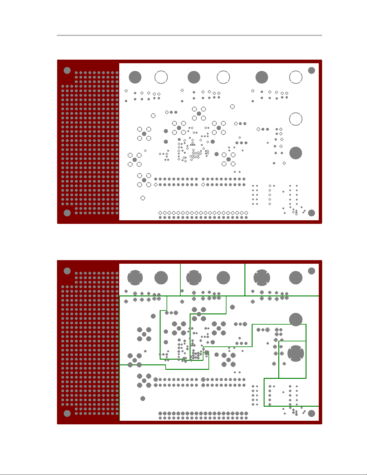
Figure 2−2.Layer 2, Ground Plane
PCB Layout
Figure 2−3.Layer 3, Power Plane
PCB Layout and Parts List
2-3
Page 14
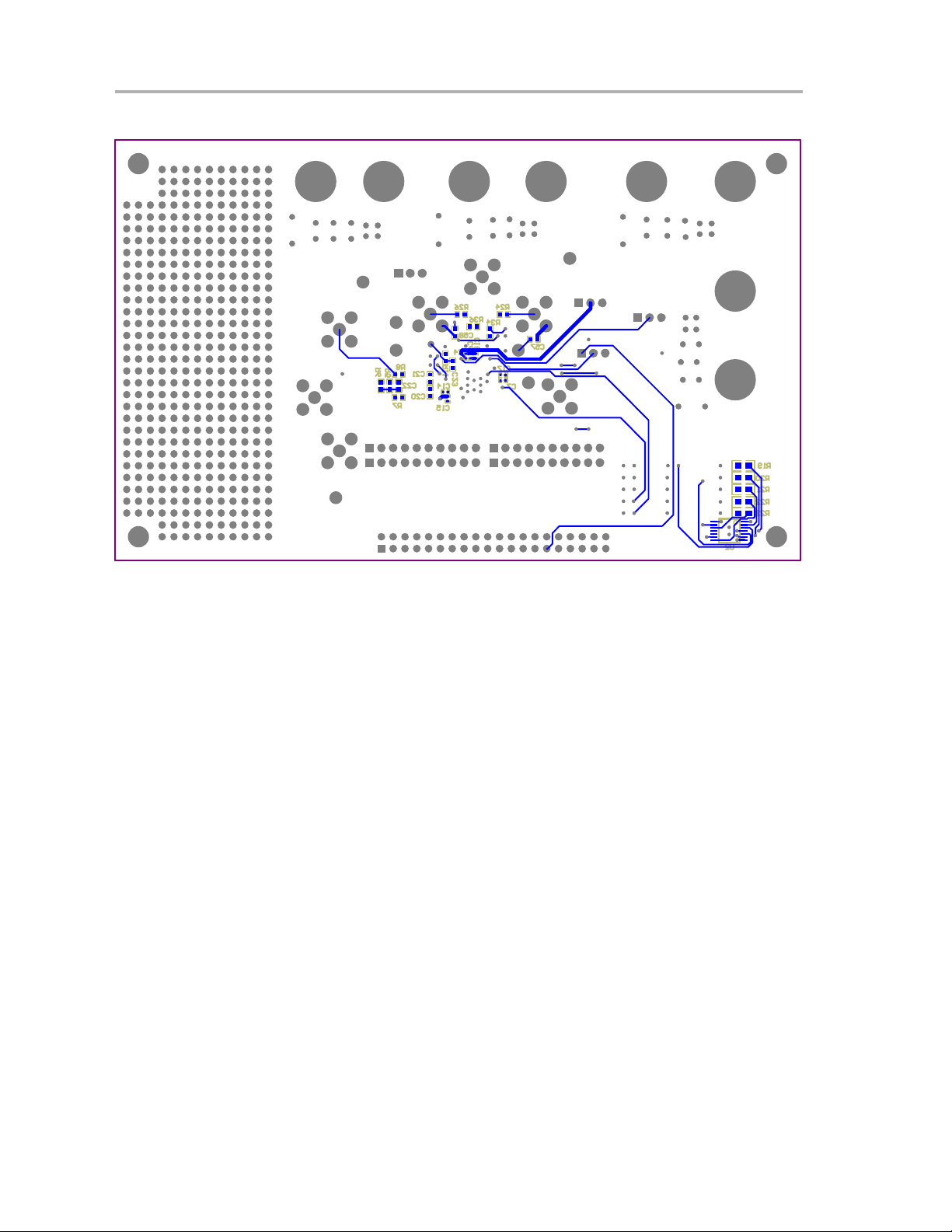
PCB Layout
Figure 2−4.Bottom Layer
2-4
Page 15

Parts List
2.2 Parts List
Table 2−1 lists the parts used in constructing the EVM.
Table 2−1.DAC5674 EVM Parts List
Ref. Des.
Description Qty. Part Number Mfg.
22-pF, 50-V, 5% capacitor 0 06035A220JAT2A AVX C20, C21
100-pF, 50-V, 5% capacitor 1 ECU-V1H101JCG Panasonic C23
0.01-µF, 16-V, 10% capacitor 2 06035A103KAT2A AVX C24, C52 C25, C55, C56
0.01-µF, 100-V, 5% capacitor 4 08055C103KAT2A AVX C42−C45
0.1-µF, 16-V, 10% capacitor 17 08055C104JAT2A AVX C1 −C7, C10,
0.1-µF, 100-V, 10% capacitor 4 ECJ-2VB1C104K Panasonic C38−C41
1-µF, 16-V, 10% capacitor 4 ECJ-3YB1C105K Panasonic C34−C37
10-µF, 10-V, 10% capacitor 4 GRM42X5R106K10 Murata C30−C33
47-µF, 10-V, 10%, tantalum
capacitor
DAC5674 1 DAC5674IDW TI U1
Ferrite bead 4 D01608C-472 Coil Craft FB1−FB4
3POS header 4 TSW-150-07-L-S Samtec W2−W5
40-pin header 1 TSW-120-07-L-D Samtec J8
Red banana jacks 4 ST-351A Allied J9, J10, J12,
Black banana jacks 4 ST-351B Allied J11, J13, J15,
Green LED 5 LN1351C-(TR) Panasonic D1−D5
0-Ω, 1/16-W, 1% resistor 1 ERJ-3EKF0R00V Panasonic R6 R5, R7−R10,
10-Ω, 1/16-W, 1% resistor 1 ERJ-3EKF10R0 Panasonic R32
49.9-Ω, 1/16-W, 1% resistor 6 ERJ-3EKF49R9V Panasonic R3, R4,
100-Ω , 1/8-W, 1% resistor 1 ERA-3YEB100 Panasonic R2
200-Ω, 1/10-W, 1% resistor 5 ERJ-6ENF2000 Panasonic R19−R23
200-Ω, 1/16-W, 0.1% resistor 2 ERA-3YEB200 Panasonic R11, R12
1-kΩ, 1/8-W, 1% resistor 0 ERJ-3EKF1001 Panasonic R35, R37
1-kΩ, 1/8-W, 1% resistor 5 ERJ-6ENF1001 Panasonic R14−R18
2-kΩ, 1/16-W, 1% resistor 1 ERJ-6ENF2001 Panasonic R1
10K-kΩ, 1/8-W, 1% resistor 2 ERJ-3EKF1002 Panasonic R13, R33
22-Ω resistor pack 2 4816P-001-220 Bourns RP1, RP2
51-Ω resistor pack 2 770-101-R51 CTS RP4, RP6 RP7, RP8
4 10TPA47M Sanyo C46−C49
Installed Not Installed
C14, C15,
C17−C19, C22,
C27, C57, C58
J14
J16
R34, R36
R24−R27
PCB Layout and Parts List
2-5
Page 16

Parts List
Table 2−1.DAC5674 EVM Parts List (Continued)
Description Qty. Part Number Mfg.
SW-PB switch 1 EVQ-PJX04M Panasonic S1
Switch 1 SD05HOSK CK S2
SMA connectors 3 713-4339
(901-144-8RFX)
SN74LVC04A 1 SN74LVC04APW TI U2
Standoff, hex (1/4 × 1”) 4 219-2063 Allied
Black test point 3 5001K Keystone TP3, TP4, TP5
Red test point 3 5000K Keystone TP1, TP2, TP6
Transformer 1 T1-1T-KK8 Mini-Circuits T1
Transformer 1 TCM4-1 Mini-Circuits T2
Allied J2, J4, J7 J1, J3, J5, J6
Installed Not Installed
Ref. Des.
2-6
Page 17

Chapter 3
Circuit Description
This chapter provides descriptions of the primary functional circuits on the
DAC5674 EVM.
Topic Page
3.1 Circuit Function 3-2. . . . . . . . . . . . . . . . . . . . . . . . . . . . . . . . . . . . . . . . . . . . . . .
Circuit Description
3-1
Page 18

Circuit Function
3.1 Circuit Function
The following paragraphs describe the EVM circuits.
3.1.1 Input Clock
The DAC5674 EVM default operation setting is with a differential input clock
sent to the DAC5674. A 500-mV p-p, 0-V offset, 50% duty-cycle external
sinewave is applied to SMA connector J4 and converted to a d i fferential clock
input to the DAC5674 by transformer T2. This input represents a 50-Ω load to
the source. In order to preserve the specified performance of the DAC5674
converter, the clock source should feature very low jitter. Using a clock with a
50% duty cycle gives optimum dynamic performance.
3.1.1.1 Differential ECL/PECL Input Clock
The EVM can be configured for differential ECL/PECL input clock mode by
configuring the board per Table 3−1 and applying the appropriate ECL/PECL
common mode voltage at terminal E1 (VTT). Use J3 and J5 to input the
external differential ECL/PECL clock signals.
3.1.1.2 Single-Ended Input Clock
The EVM can be configured for single-ended input clock mode by configuring
the board per T able 3−1. SMA connector J3 or header J8 can be used to input
the external TTL/CMOS clock signal.
Table 3−1.EVM Clock Configuration
Clock Configuration Components Installed
Sinewave (Default) R12, T2, C52 R9, R10, R34, R35, R36, R37,
ECL or PECL R9 (0.01-µF cap.), R10 (0.01-µF
cap.)
Single ended TTL/CMOS from J3 R9, C55 R10, R12, R25, R34, R35, R37,
Single ended TTL/CMOS from J8 R34, R37, C55 R9, R10, R12, R35, T2, C56
†
All component values are per the schematic except where shown in parentheses.
†
Components Not Installed
C55, C56
R36, R12, R34, R35, R37, T2,
C55, C56
T2, C56
3.1.2 Input Data
The DAC5674 EVM can accept 3.3-V CMOS logic level data inputs through
the 40-pin header J8 per Table 3−2. The board provides 50-Ω termination to
ground and series dampening resistors to minimize digital ringing and
switching noise. J8 also provides a path for an input clock (see Table 3−1 for
proper board configuration).
3-2
Page 19

Circuit Function
Table 3−2.Input Connector J8
J8 Pin Description J8 Pin Description J8 Pin Description
1 CMOS data bit 13 (MSB) 15 CMOS data bit 6 29 Reset
2 GND 16 GND 30 GND
3 CMOS data bit 12 17 CMOS data bit 5 31
4 GND 18 GND 32 GND
5 CMOS data bit 11 19 CMOS data bit 4 33
6 GND 20 GND 34 GND
7 CMOS data bit 10 21 CMOS data bit 3 35
8 GND 22 GND 36 GND
9 CMOS data bit 9 23 CMOS data bit 2 37
10 GND 24 GND 38 GND
11 CMOS data bit 8 25 CMOS data bit 1 39 SCLK_IN
12 GND 26 GND 40 GND
13 CMOS data bit 7 27 CMOS data bit 0 (LSB)
14 GND 28 GND
3.1.3 Output Data
The DAC5674 EVM can be configured to drive a doubly terminated 50-Ω cable
or provide unbuffered differential outputs.
3.1.3.1 Transformer Coupled Signal Output
The factory-set configuration of the demonstration board provides the user
with a single-ended output signal at SMA connector J7. The DAC5674 is
configured to drive a doubly terminated 50-Ω cable using a 1:1 impedance
ratio transformer, a 100-Ω terminating resistor R2, and the center tap of T1
connected to ground per Table 3−3. When using a 4:1 impedance ratio
transformer, configure the EVM per Table 3−3. The common mode input
voltage of T1 can be adjusted by using the resistor divider network R5 and R6.
Table 3−3.Transformer Output Configuration
Configuration Components Installed
1:1 Impedance ratio transfomer R2, R3, R4, R6, C22, T1 (1:1) R5, R7, R8, C20, C21
4:1 Impedance ratio transfomer R3 (100), R4 (100), R6, C22,
T1 (4:1)
†
All component values are per the schematic except where shown in parenthesis.
3.1.3.2 Unbuffered Differential Output
†
Components Not Installed
R2, R5, R7, R8, C20, C21
To provide unbuffered differential outputs, the EVM must be configured as
follows: remove R2, C20, C21, and T1; Install R3, R4, R7, R8, J1 and J6.
Circuit Description
3-3
Page 20

Circuit Function
3.1.4 Internal Reference Operation
The full-scale output current is set by applying an external resistor (R1)
between the BIASJ pin of the DAC5674 and ground. The full-scale output
current can be adjusted from 20 mA down to 2 mA by varying R1 or changing
the externally applied reference voltage. The full-scale output current,
IOUT
, is defined as follows:
FS
IOUT
= 32 × (V
FS
EXTIO
/R1)
where V
is the voltage at pin EXTIO. This voltage is 1.2 V typical when
EXTIO
using the internally provided bandgap reference voltage source.
3.1.5 External Reference Operation
The internal reference can be disabled and overridden by an external
reference by connecting a voltage source to terminal TP2 (EXT_I/O) and
connecting EXTLO to AVDD. The specified range for external reference
voltages should be observed (see the DAC5674 data sheet (SLWS148) for
details).
3.1.6 Sleep Mode
The DAC5674 EVM provides a means of placing the DAC5674 into a
power-down mode. This mode is activated by placing jumper W3 between pins
2 and 3.
3.1.7 Filter Control
The DAC5674 has two inputs, HP1 and HP2, which control the internal
interpolation filters (FIR1 and FIR2) mode of operation. When these inputs are
set to a logic high, the filters are configured for high-pass response. When set
to a logic low, the filters are configured for low-pass response. A third input,
X4, allows the user to bypass Interpolation Filter 1. When X4 is set to a logic
low, Filter 1 is bypassed. See the data sheet (SL WS148) for more information.
3.1.8 PLL Divider Control
The DAC5674 has two inputs, DIV0 and DIV1, which control the internal PLL
prescaler divide ratio setting. These two signals, along with the three filter
control signals, are all controlled by DIP switch S2 on the EVM. All control
signals are in the logic low level when the DIP switch is in the closed position.
See the data sheet (SLWS148) for more information.
3-4
Page 21

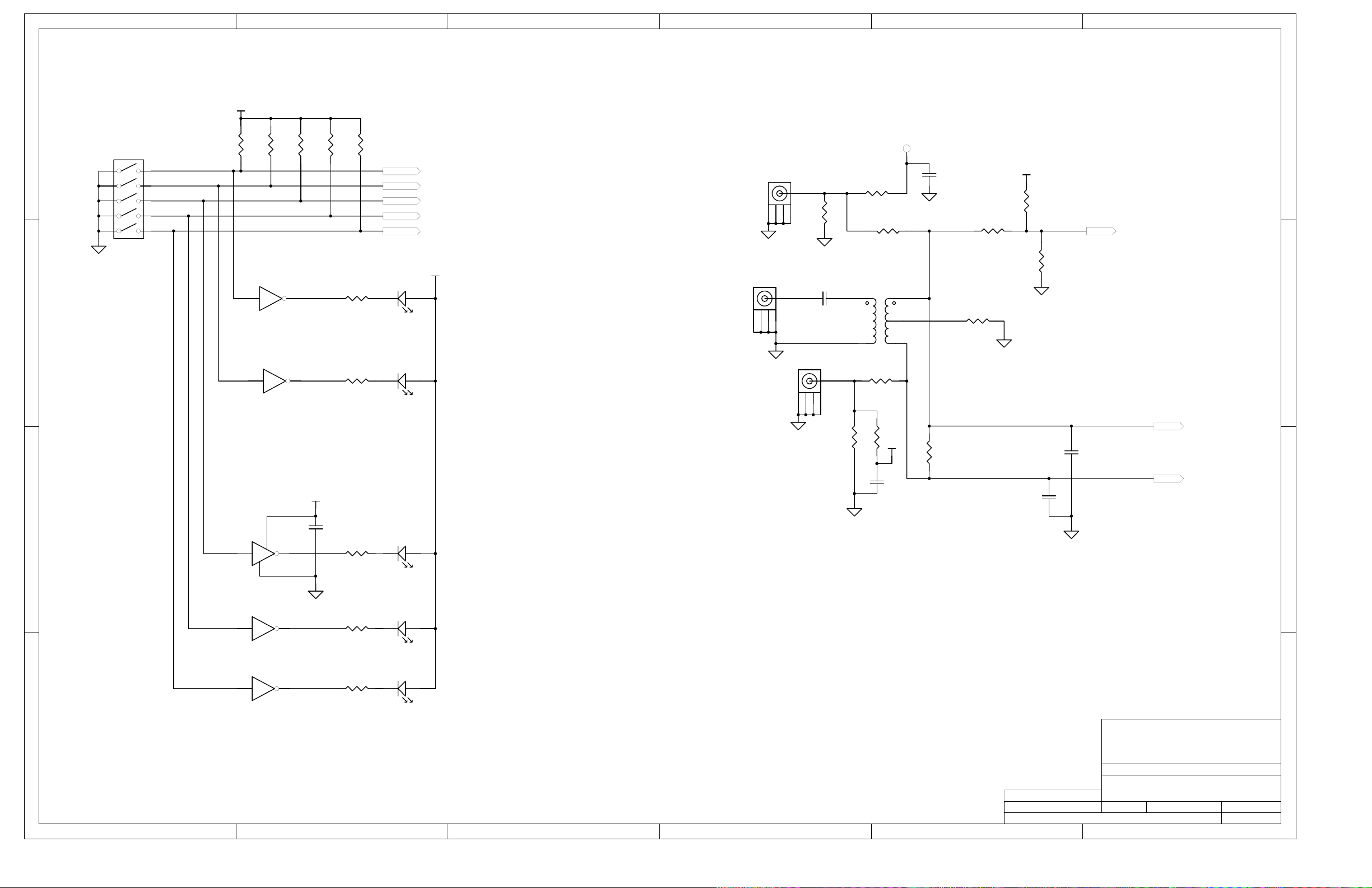
This chapter contains the EVM schematic diagrams.
Chapter 4
Schematics
Schematics
4-1
Page 22

D
SCLK
C
B
12
34
56
78
910
1112
1314
1516
1718
1920
2122
2324
2526
2728
2930
3132
3334
3536
3738
3940
40PIN_IDC
54321
REV ECN Number Approved
J6
(Note 1)
SMA
C24
.01uF
3
J2
SMA
W5
1
3 4
5
2
R7
0
(Note 1)
C22
R6
0
.1uF
+3.3VCLK
S1
3
SW-PB
.1uF
3
2
1
R8
0
1
2
C4
3 4
C10
.1uF
R13
10K
T1
T1-1T-KK81
J1
SMA
(Note 1)
5
C6
.1uF
+3.3VA
(Note 1)
R3
49.9R449.9
1
2
R33
10K
R5
0
W4
1
2
3 4
5
2
1
+1.8_3.3VD
RP7
(Note 1)
10PIN_SIP_RPACK
10
9
8
7
6
5
4
3
RP8
RP1
RP2
2
10
9
8
7
6
5
4
3
2
22
22
SCLK
1
(Sh 3)
RP4
10PIN_SIP_RPACK
2
3
4
5
6
7
8
9
10
1
1
(Note 1)
10PIN_SIP_RPACK
J8
D13_IN
D12_IN
D11_IN
D10_IN
D9_IN
D8_IN
D7_IN
D6_IN
D5_IN
D4_IN
D3_IN
D2_IN
D1_IN
D0_IN
RESET
SCLK_IN
R32
10
1 16
2 15
3 14
4 13
5 12
6 11
7 10
8 9
1 16
2 15
3 14
4 13
5 12
6 11
7 10
8 9
SCLK
.1uF
C3
D13
D12
D11
D10
D9
D8
D7
D6
D5
D4
D3
D2
D1
D0
.1uF
C1
.1uF
1
2
3
4
5
6
7
8
9
10
11
12
+3.3VA
C14
.1uF
+1.8VD
C15
48
DGND
DGND
D13
D12
D11
D10
D9
D8
D7
D6
D5
D4
HP1
HP2
X4
AVDD45AVDD46DVDD47DVDD
D313D214D115D016HP117HP218DGND19IOGND20DVDD21IODVDD22X423GND
HP1
HP2
X4
44
42
43
AGND
IOUT2
IOUT1
U1
DAC5674
(Sh 3)
(Sh 3)
(Sh 3)
(Sh 3)
C21
22pF
E2
RESET
R2
100
C23
100 pF
TP6
RED
R11
200, 1%
TP1
RED
R1
2K
+3.3VA
41
39
40
38
BIASJ
AGND
EXTIO
EXTLO
PLLLOCK
3
37
AGND
SLEEP
LPF
PLLVDD
PLLGND
CLKVDD
CLKGND
CLKC
CLK
DIV0
DIV1
RESET
24
1
2
C5
.1uF
W2
+1.8VD
36
35
34
33
32
31
30
29
28
27
26
25
TP2
RED
C2
.1uF
CLKC
CLK
DIV0
DIV1
+1.8_3.3VD
C17
.1uF
+1.8_3.3VD
W3
1
2
(Note 1) (Note 1) (Note 1)
C20
22pF
3
CLKC
CLK
DIV0
DIV1
Revision History
4
6
+3.3VCLK
+1.8_3.3VD
6
D
1
C18
.1uF
J7
3 4
I_OUT
5
2
C
B
1
A
10PIN_SIP_RPACK
RP6
2
3
4
5
6
7
8
9
10
NOTE 1. PART IS NOT INSTALLED
1 2 3 4 56
.1uF
C7
C19
.1uF
A
ti
12500 TI Boulevard. Dallas, Texas 75243
Title:
Engineer:
Drawn By:
FILE:
J. SETON
Y. DEWONCK
SIZE:
DAC5674
DATE: REV:
4-Sep-2003
SHEET: OF:
B
1
3
Page 23

54321
6
D
+3.3V ANALOG
J9
RED
J11
BLACK
C
3VA
FB1
FERRITE
+
10uF
C30
C34
1uF
C38
.1uF
1.8V / +3.3V DIGITAL
J12
3VD
RED
J15
BLACK
FB3
FERRITE
+
10uF
C32
C36
1uF
C40
.1uF
C42
.01uF
+1.8_3.3VD
C44
.01uF
+3.3VA
+
+
C46
47 uF
C48
47 uF
+3.3V CLOCK
J10
RED
J13
BLACK
+1.8VD
J14
RED
J16
BLACK
VCLK
18VD
FB2
FERRITE
FB4
FERRITE
+
10uF
+
10uF
C31
C33
C35
1uF
C37
1uF
C39
.1uF
C41
.1uF
C43
.01uF
C45
.01uF
+3.3VCLK
+
+1.8VD
+
C47
47 uF
C49
47 uF
D
C
B
TP3
BLACK
A
TP4
BLACK
TP5
BLACK
B
A
ti
12500 TI Boulevard. Dallas, Texas 75243
Title:
Engineer:
J. SETON
Drawn By:
Y. DEWONCK
FILE:
1 2 3 4 56
SIZE:
DAC5674
DATE: REV:
4-Sep-2003
SHEET: OF:
B
23
Page 24
54321
+1.8_3.3VD
D
R141KR15
S2
10_SM_SWITCH
1 10
2 9
3 8
4 7
5 6
C
B
1 2
1K
U2B
3 4
SN74LVC04A
U2C
5 6
SN74LVC04A
14
U2A
SN74LVC04A
7
+1.8_3.3VD
R16
1K
C27
.1uF
R17
1K
DIV1
DIV0
HP2
HP1
X4
R20
200
R19
200
R21
200
R18
1K
GREEN
GREEN
GREEN
D1
D2
D3
E1
VTT
R34
0
+3.3VCLK
R35
49.9
(Note 1)
(Note 1)
R37
49.9
(Note 1)
(Note 1)
SCLK
C55
.01uF
C57
.1uF
(Note 1)
6
5
4
(Note 1)
R36
0
R12
200
(Note 1)
5
J3
SMA
5
3 4
2
J5
SMA
(Note 1)
49.9
R26
R25
49.9
(Note 1)
R9
0
T2
1
3
TCM4-1
(Note 1)
R10
0
R27
49.9
VTT
C58
.1uF
1
3 4
2
1
R24
49.9
C52
.01uF
1
3 4
5
2
(Sh 1)
DIV1
(Sh 1)
DIV0
(Sh 1)
HP2
(Sh 1)
HP1
(Sh 1) (Sh 1)
X4
+3.3VCLK
J4
SMA
INPUT CLOCK
SCLK
CLK
C56
.01uF
CLKC
CLK
CLKC
6
D
C
(Sh 1)
(Sh 1)
B
U2D
9 8
SN74LVC04A
U2F
13 12
SN74LVC04A
A
R22
200
R23
200
D4
GREEN
D5
GREEN
A
ti
12500 TI Boulevard. Dallas, Texas 75243
NOTE 1. PART IS NOT INSTALLED
1 2 3 4 56
Engineer:
Drawn By:
FILE:
J. SETON
Y. DEWONCK
Title:
SIZE:
DAC5674
DATE: REV:
4-Sep-2003
SHEET: OF:
B
33
 Loading...