

Texas Instruments DAC38RF8xEVM Series, DAC38RF82EVM, DAC38RF80EVM, DAC38RF86EVM, DAC38RF89EVM User Manual
...Page 1

User's Guide
SLAU671A–October 2016–Revised March 2017
DAC38RF8xEVM
The DAC38RF8xEVM is the family of circuit boards for evaluating the DAC38RFxx family of high-speed
digital-to-analog converters (DACs) from Texas Instruments. The DAC38RF8xEVM family consists of the
DAC38RF80EVM, DAC38RF87EVM, DAC38RF82EVM, DAC38RF86EVM, and DAC38RF89EVM. This
user's guide is applicable to all the EVMs in the DAC38RF8xEVM family. This document is intended to
guide the DAC38RF8xEVM user through the process of setting up the EVM successfully. For other
information on the DAC38RFxx device family, refer to the device datasheet (SLASEA3, SLASEA6, and
SLASEF4). Throughout this document, italics are used to refer to names of controls on graphical user
interfaces (GUI).
Contents
1 Introduction ................................................................................................................... 2
1.1 Required Hardware and Software ................................................................................ 2
1.2 Hardware Description .............................................................................................. 2
2 Quick Start.................................................................................................................... 5
2.1 TSW14J56 and DAC38RF8xEVM................................................................................ 5
3 Generating Configuration Files for Custom Boards.................................................................... 15
3.1 Status Log.......................................................................................................... 15
3.2 Low Level View.................................................................................................... 15
Appendix A ....................................................................................................................... 17
Appendix B ....................................................................................................................... 18
List of Figures
1 DAC38RF8xEVM Block Diagram.......................................................................................... 2
2 Shunt Pin 1 and Pin 2 of JP10 Jumper Enabling External Clock Mode.............................................. 5
3 DAC38RF83 EVM Setup for External Clock Mode...................................................................... 6
4 DAC38RF8xEVM GUI Quick Start Page Configured for External Clock Mode ..................................... 7
5 DAC38RF8xEVM GUI External Clock Select Checkbox ............................................................. 7
6 Open Pin 1 and Pin 2 of JP10 Jumper to Enable On-Chip PLL Clock Mode........................................ 8
7 DAC38RF83 EVM Setup for On-Chip PLL Mode ....................................................................... 9
8 DAC38RF8xEVM GUI Quick Start Page Configured for On-Chip PLL Mode...................................... 10
9 Load Firmware to the TSW14J56........................................................................................ 11
10 Complex, Single Tone Generation at 100 kHz in HSDC Pro......................................................... 11
11 DAC A Digital Control Tab of the DAC38RF8x GUI ................................................................... 12
12 DAC A Output at 1960 MHz and 2140 MHz, Mixer Gain Off, Dummy Date Enabled............................. 13
13 1×20 MHz LTE, TM3.1, Center Frequency = 1960 MHz, DAC Coarse Gain = 10, External Clock............. 13
14 1×20 MHz LTE, TM3.1, Center Frequency = 2140 MHz, DAC Coarse Gain = 10, External Clock............. 14
15 DAC Output Power vs Frequency (Fsampling = 8847.36 Msps) .................................................... 14
16 DAC38RF8xEVM GUI Status Log ....................................................................................... 15
17 DAC38RF8xEVM GUI Low Level View ................................................................................. 16
18 DAC Output Circuit Schematic ........................................................................................... 17
19 TCM3-452X-1+ Frequency Response................................................................................... 17
20 Clock Input Path Circuit Diagram ........................................................................................ 18
21 NCR2-113+ Frequency Response....................................................................................... 18
SLAU671A–October 2016–Revised March 2017
Submit Documentation Feedback
Copyright © 2016–2017, Texas Instruments Incorporated
DAC38RF8xEVM
1
Page 2
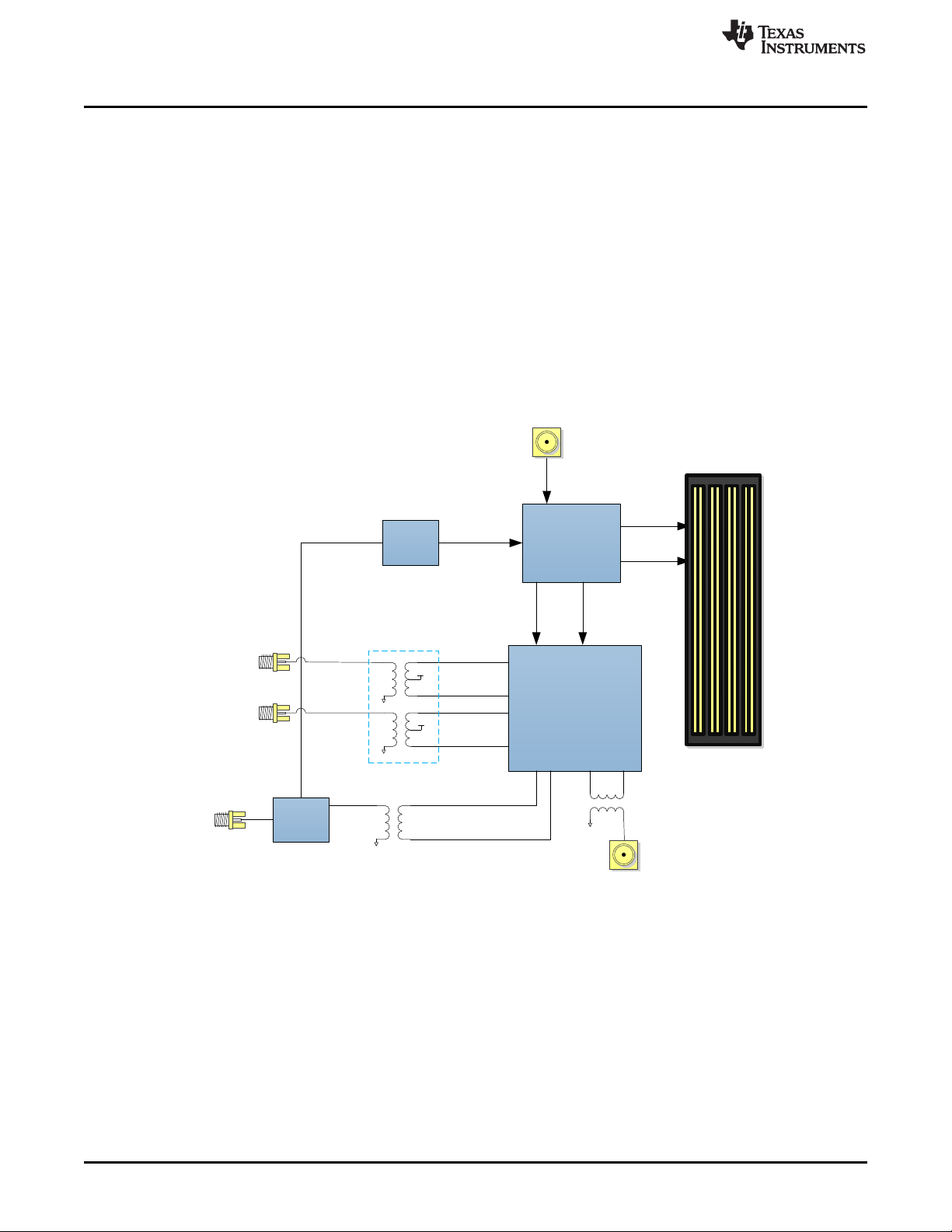
1:2 Power
Splitter
DA38RF8x
LMK04828
Clock
Divider
(/4)
IOUTA+
IOUTA>
IOUTB>
IOUTB+
Sysref
Reference
Clock
SMA
SMA J1
SMA
SMA
NCR2-113+
2:1
TCM3-452X-1+
2:1
NB7V33M
FMC Connector
Sysref
Reference
Clock
1.8 V
1.8 V
+ CLKTX>
SMA
+ CLKIN >
TCM2-43X+
2:1
Introduction
1 Introduction
1.1 Required Hardware and Software
The following hardware and software are required to evaluate the DAC38RF8x device:
1. DAC38RF8xEVM: Main circuit board containing the DAC to be evaluated
2. DAC38RF8xEVM Graphical User Interface (GUI): Software that controls the DAC EVM:
http://www.ti.com/tool/TSW14J56EVM
3. TSW14J56 EVM: Hardware that generates digital patterns for the DAC:
http://www.ti.com/tool/TSW14J56EVM
4. HSDC Pro software: Software interface that controls the TSW14J56 EVM. Version 4.50 or higher is
recommended: http://www.ti.com/tool/dataconverterpro-sw
1.2 Hardware Description
Figure 1 illustrates the EVM block diagram.
www.ti.com
2
DAC38RF8xEVM
Figure 1. DAC38RF8xEVM Block Diagram
Copyright © 2016–2017, Texas Instruments Incorporated
SLAU671A–October 2016–Revised March 2017
Submit Documentation Feedback
Page 3
www.ti.com
Introduction
Table 1. DAC38RF8xEVM Component Description
Part Description
DAC38RF8x 9 Gsps dual-channel DAC with JESD204B interface
FMC Connector Interface to connect DAC evaluation board to pattern generators (for example, TSW14J56)
LMK04828 JESD204B-compliant clock generator. Used to generate SYSREF and device clock to pattern generator. Also
NB7V33M 10 GHz divide by 4 clock divider
TCM3-452X-1+ 2:1 impedance ratio transformer. Used for (1) impedance matching to 50-Ω load, (2) differential to single-ended
TCM2-43X+ 2:1 impedance ratio transformer. Used to convert CLKTX from differential to single ended. CLKTX is divided by 3 or 4
NCR2-113+ 2:1 impedance ratio transformer. Used to convert single-ended input clock to differential for the DAC.
generates SYSREF and PLL reference clock to DAC38RF8x.
conversion, (3) DC biasing of DAC output.
output of the DAC sampling clock.
Table 2. Jumpers on DAC38RF8xEVM
Jumper Default Position Description
JP1 Shunt pin 2-3 shunt pin1-2: Put some DAC internal blocks in sleep mode.
JP2 Shunt pin 2-3 shunt pin1-2- Enable DAC output.
JP3 Open Open: Disables power to the on-board 122.88 MHz VCXO (Y1). Leave open
JP8 Open Open: Enables VDDDIG1 supply (U37).
JP9 Open Open: Enables VEE18N supply (U19).
JP10 Shunt pin 1-2 Closed: Enable external clock mode
J11 Open Not used
J22 Open Provides access to externally monitor ATEST pin
J23 Shunt pin 1-2, 3-4, 5-6, 7-8 Connects DAC SPI interface to FT2232H (U4) spi interface.
Shunt pin2-3: Take DAC out of sleep mode
Shunt pin2-3-disable DAC output
when VCXO is not used
Closed: Enables power to the on-board 122.88 MHz VCXO
Closed: disables VDDDIG1 supply (U37)
Closed: disables VEE18N supply (U19)
Open: Enable on-chip PLL clock mode
1.2.1 Clocking Modes
The DAC38RF8xEVM may be configured into one of five clocking modes. These clocking modes are:
1. Direct External clock mode with high amplitude clock
2. Direct External clock mode with low amplitude clock (less than 7 dBm)
3. On-chip PLL clock mode
4. On-board VCXO clock mode
5. LMF = 413 or 823, 12-bits clock mode
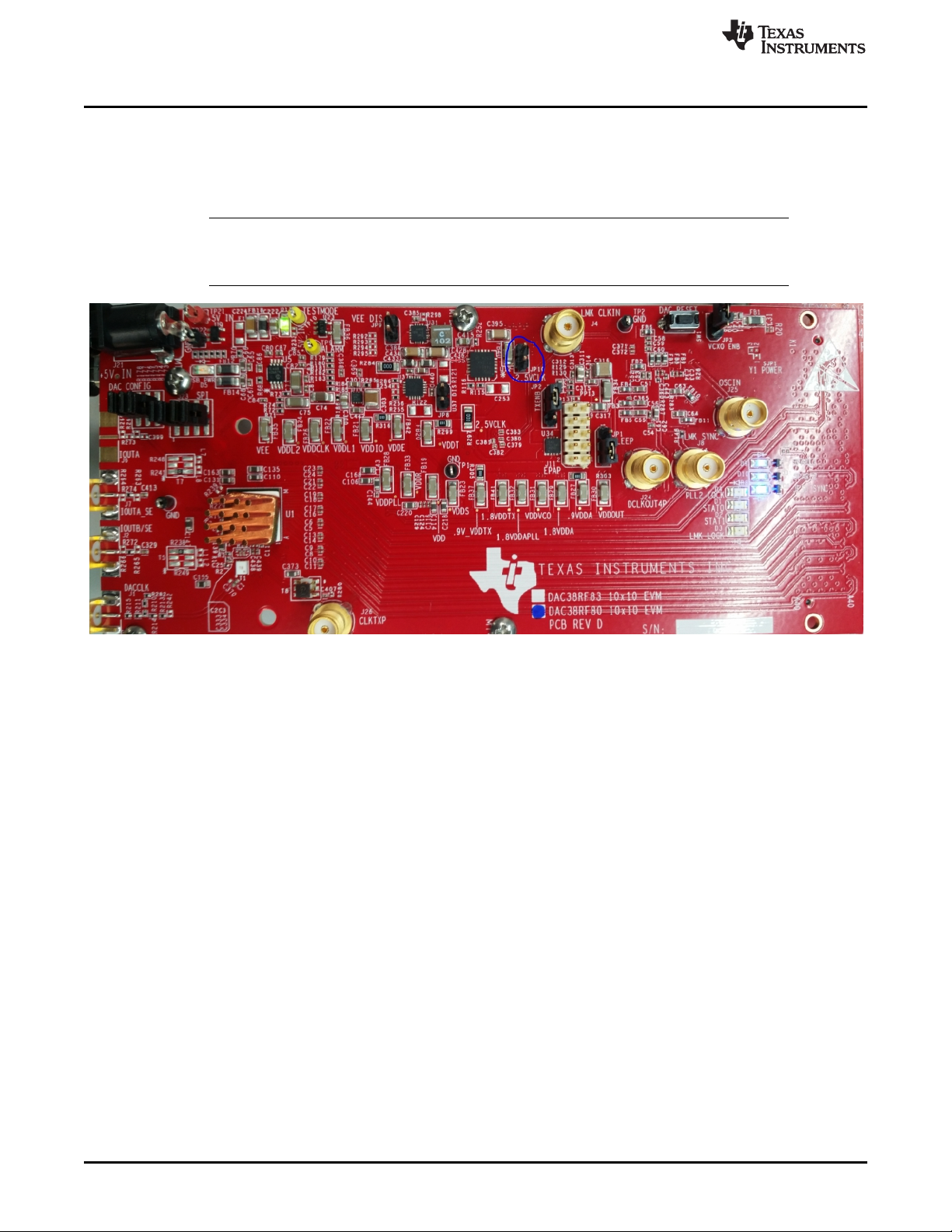
1.2.1.1 Direct External Clock Mode With High Amplitude Clock (CMODE1)
This mode is intended for use with signal generators that can output 16 dBm or higher. Examples are
Keysight E8257D or R&S SMA100. To use this mode, the only modification from the default EVM
configuration is to connect a shunt between pin 1 and 2 of jumper JP10. Then, provide a 16-dBm clock to
SMA J1. This is shown in Figure 2. By default, the EVM is configured to use the single-ended clock input
of the DAC in this mode. For best spurious performance, also install C1, C333, and C334 on the EVM to
switch to differential clock input of DAC. Refer to the schematics and BOM of the EVM for the component
values (SLAC734).
SLAU671A–October 2016–Revised March 2017
Submit Documentation Feedback
Copyright © 2016–2017, Texas Instruments Incorporated
DAC38RF8xEVM
3
Page 4

Introduction
1.2.1.2 Direct External Clock Mode With Low Amplitude Clock (CMODE2)
The purpose of this mode is for use with monolithic clock synthesizers like the LMX259x. Clock power in
the range of 3 dBm to 7 dBm is recommended in this mode. Note that when using the LMX2592 with the
frequency doubler enabled, an external filter is required to attenuate the sub-harmonic at half the clock
frequency to –50 dBc or better. To configure the EVM in this mode from the default configuration:
1. Install SMA J27
2. Remove C2, C3, R215, R211
3. Install R323, R324, C449, C450 (refer to the schematics and BOM of the EVM for the component
values (SLAC734)
4. Connect the positive and negative output of clock synthesizer to SMA J27 and SMA J1, respectively
5. Remove jumper JP10
6. Use a second signal generator to provide a clock to SMA J4 and set the amplitude to 6 dBm. The
frequency of this clock is one-fourth of the sampling rate (or Fs/4). This clock is used to provide the
reference clock of the FPGA and SYSREF.
7. Connect SMA J24 to the reference input of the clock synthesizer. The frequency at SMA J24 is set
from the EVM GUI in a later step.
1.2.1.3 On-Chip PLL Clock Mode (CMODE3)
This mode is for evaluating the DAC performance with a low-frequency reference clock and the internal
PLL/VCO as the sampling clock. To use this mode, connect a clock at 6 dBm to SMA J4 and remove the
shunt connecting pin1 and 2 of jumper JP10. Keep all other hardware settings in the default configuration.
The frequency of the clock at SMA J4 is determined from the EVM GUI in a later step.
www.ti.com
1.2.1.4 On-Board VCXO Clock Mode (CMODE4)
This mode allows the DAC to be evaluated without providing any external clock. The on-board VCXO
running at a fixed 122.88-MHz frequency can be used to provide a reference clock to the LMK04828 PLL.
The high-frequency clock generated by the LMK04828 PLL is subsequently divided down and used to
source reference clock and SYSREF to the DAC internal PLL and the FPGA on TSW14J56 EVM. To use
this mode, connect a shunt between pins 1 and 2 of jumper JP3. Keep all other hardware settings in the
default configuration.
1.2.1.5 LMF = 413 or 823, 12-Bits Clock Mode(CMODE5)
This mode is used to generate the required clocks for evaluating the DAC in 12-bits mode, LMF = 413 or
823 only. Two signal generators with their 10-MHz reference connected together are required in this
mode. The setup involves:
1. Provide an external sampling clock to SMA J1
2. Provide a second clock to SMA J4 with an amplitude of 6 dBm. The frequency of this clock will be
determined by the EVM GUI in a later step. Connect the reference of the two signal generators
together.
3. Remove the shunt on pins 1 and 2 of jumper JP10
4
DAC38RF8xEVM
Copyright © 2016–2017, Texas Instruments Incorporated
SLAU671A–October 2016–Revised March 2017
Submit Documentation Feedback
Page 5
www.ti.com
2 Quick Start
The following examples use an external clock and the on-chip PLL to evaluate the performance of the
DAC38RF8xEVM. The frequency of the clock is arbitrarily selected as 6144 Msps but the procedure
outlined is applicable to any external clock frequency and any supported on-chip PLL frequency.
The external clock path includes a balun for single-ended to differential conversion. Appendix B shows the
insertion loss, amplitude, and phase un-balance of this balun.
2.1 TSW14J56 and DAC38RF8xEVM
This section covers details on the TSW14J56 and DAC38RF8xEVM.
1. Make sure both boards are not powered and not connected to the USB port of the PC.
2. Connect the FMC connector of TSW14J56 EVM (J4) to FMC connector of DAC38RF8xEVM (J20).
2.1.1 TSW14J56
1. Connect a 5-V power supply to connector J11 (+5 V IN).
2. Connect a USB cable to the USB connector (J9).
3. Flip the power switch (SW6) to the “ON” position.
2.1.2 DAC38RF8xEVM Configuration With Direct External Clock(CMODE1)
Skip this section if the on-chip PLL is used as the DAC clock source.
Quick Start
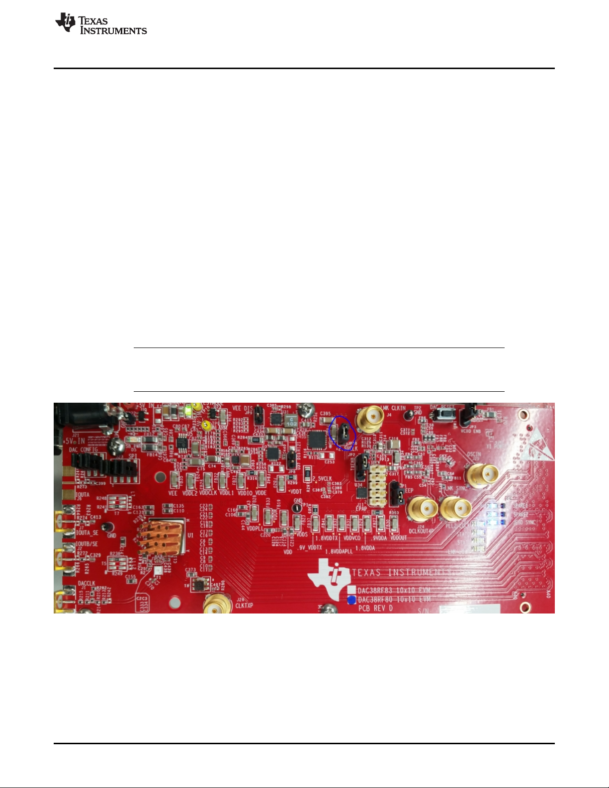
NOTE: Shunt pin 1 and pin 2 of the 2-pin jumper labeled JP10 to enable external clock mode. This
is shown in Figure 2. Other hardware changes may be required depending on the external
clocking mode. These changes are described in Section 1.2.1.
Figure 2. Shunt Pin 1 and Pin 2 of JP10 Jumper Enabling External Clock Mode
SLAU671A–October 2016–Revised March 2017
Submit Documentation Feedback
Copyright © 2016–2017, Texas Instruments Incorporated
DAC38RF8xEVM
5
Page 6
Quick Start
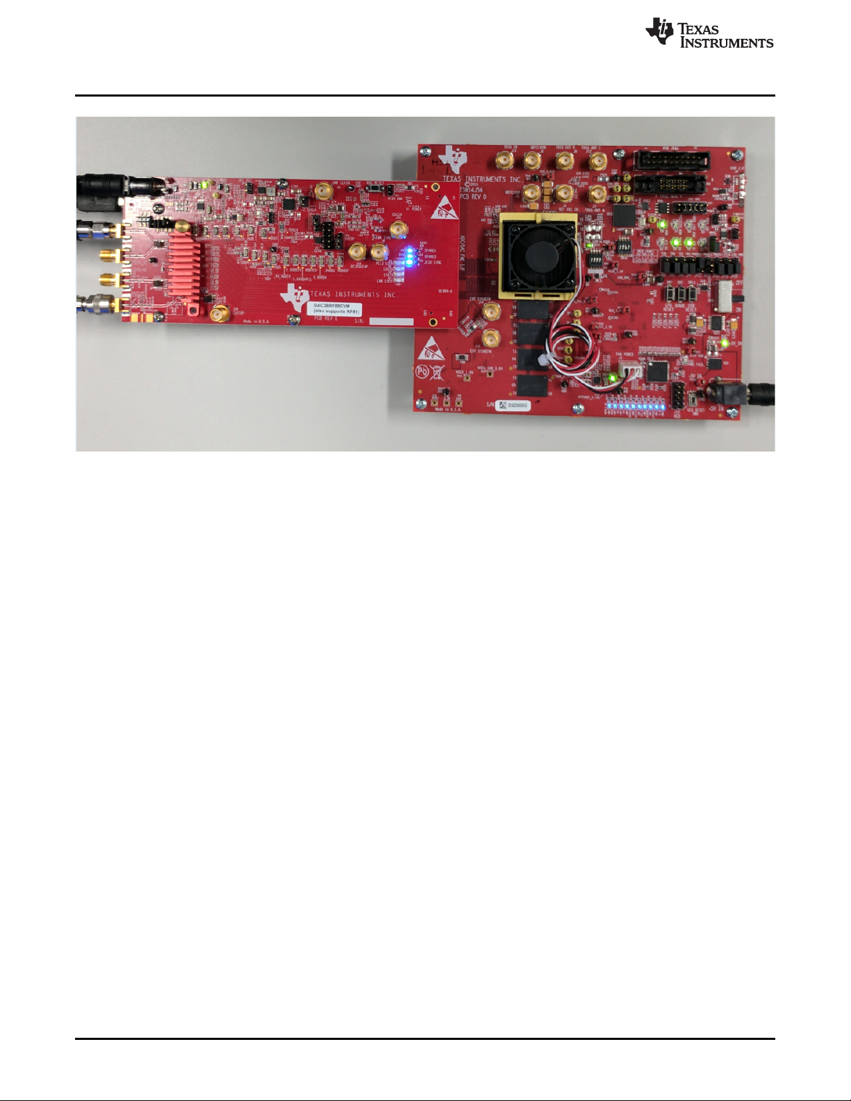
www.ti.com
Figure 3. DAC38RF83 EVM Setup for External Clock Mode
1. Connect a 5-V power supply to connector J21 (+5V_IN).
2. Connect a USB cable to the USB connector (J16).
3. Provide a 16-dBm, 6144-MHz, external DAC sampling clock to the clock balun input at J1.
4. Connect a spectrum analyzer to the DAC output SMA connector:
• For DAC38RF83: Connect spectrum analyzer to J6 (DAC A output) or J2 (DAC B output).
• For DAC38RF80: Connect a spectrum analyzer to J7 (DAC A output) or J2 (DAC B output).
2.1.3 DAC38RF8x Graphical User Interface (GUI)
Follow these steps to use the DAC38RF8x GUI:
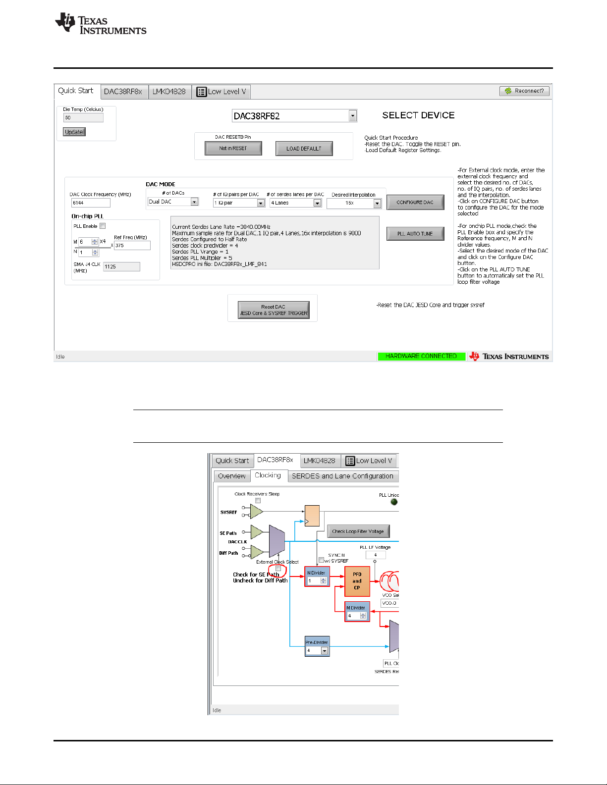
1. Start the DAC38RF8xEVM GUI, then navigate to the quick start page as shown in Figure 4.
2. Verify that the green USB Status indicator on the top right corner is lit. If it is not lit, click the
Reconnect FTDI? button and check the USB Status indicator again.
3. From the Quick Start tab, in the SELECT DEVICE drop down menu, choose from the list of available
devices. The device list is automatically populated based on the type of EVM connected.
4. On the Quick Start tab, toggle the DAC RESETB Pin button and then click on the Load Default
button. The software automatically configures the DAC to its default state.
5. Enter the desired DAC clock frequency (6144 MHz in this example) and specify the desired number of
DACs (Dual DAC), number of IQ pairs (1 IQ pair), number of lanes (4 lanes), and interpolation (16x) as
shown in Figure 4.
6. Note the messages displayed for information about the SerDes rate, maximum allowed sample rate for
the selected mode, and the HSDC Pro ini file to select (see the section on HSDC Pro for more
information). If the DAC clock frequency entered is not supported for the selected mode, the DAC clock
frequency box blinks.
6
DAC38RF8xEVM
Copyright © 2016–2017, Texas Instruments Incorporated
SLAU671A–October 2016–Revised March 2017
Submit Documentation Feedback
Page 7
www.ti.com
Quick Start
Figure 4. DAC38RF8xEVM GUI Quick Start Page Configured for External Clock Mode
7. Click on the CONFIGURE DAC button to load the DAC configuration data.
NOTE: When using CMODE2 and after configuring the DAC in the preceding step 6, navigate to
DAC38RF8x>>Clocking tab and de-select the External Clock Select checkbox.
Figure 5. DAC38RF8xEVM GUI External Clock Select Checkbox
SLAU671A–October 2016–Revised March 2017
Submit Documentation Feedback
Copyright © 2016–2017, Texas Instruments Incorporated
DAC38RF8xEVM
7
Page 8
Quick Start
8. Click on the Reset DAC JESD Core button and the Trigger LMK04828 SYSREF button.
2.1.4 DAC38RF8xEVM Configuration With On-Chip PLL(CMODE3)
Skip this section if using an external clock such as the DAC clock source.
NOTE: The 2-pin jumper labeled JP10 must be open to enable on-chip PLL clock mode. This is
shown in Figure 6. Other hardware changes may be required depending on the on-chip PLL
clocking mode selected. These changes are described in Section 1.2.1.
www.ti.com
Figure 6. Open Pin 1 and Pin 2 of JP10 Jumper to Enable On-Chip PLL Clock Mode
8
DAC38RF8xEVM
Copyright © 2016–2017, Texas Instruments Incorporated
SLAU671A–October 2016–Revised March 2017
Submit Documentation Feedback
Page 9

www.ti.com
Quick Start
Figure 7. DAC38RF83 EVM Setup for On-Chip PLL Mode
1. Connect a 5-V power supply to connector J21 (+5 V IN).
2. Connect a USB cable to the USB connector (J16).
3. Provide a 4–8 dBm external reference clock to SMA J4 as shown in Figure 7. The frequency of this
reference clock is set in a later step.
4. Connect a spectrum analyzer to the DAC output SMA connector.
2.1.5 DAC38RF8x Graphical User Interface (GUI)
1. Start the DAC38RF8xEVM GUI then navigate to the quick start page as shown in Figure 8.
2. Verify that the green USB Status indicator on the top right corner is lit. If it is not lit, click the
Reconnect FTDI? button and check the USB Status indicator again.
3. On the Quick Start tab, toggle the DAC RESETB Pin button and then click the Load Default button.
The software automatically configures the DAC to its default state.
4. Check the PLL Enable box and enter the desired on-chip PLL reference clock frequency.
NOTE: The DAC Clock Frequency box automatically updates based on the M, N, and Ref Freq
values entered. If the calculated DAC clock frequency is not supported by the on-chip PLL,
the DAC Clock Frequency box blinks.
For this example:
(a) If using DAC38RF80EVM, DAC38RF87EVM, or DAC38RF82EVM set the reference
frequency to 384 MHz, M = 4 and N = 1. The DAC PLL clock frequency is 6144 MHz.
(b) If using DAC38RF86EVM, set the reference frequency to 368.64 MHz, M = 6 and N = 1.
The DAC PLL clock frequency is 8847.36 MHz.
(c) If using DAC38RF89EVM, set the reference frequency to 307.2 MHz, M = 4 and N = 1.
The DAC PLL clock frequency is 4915.2 MHz.
5. Specify the desired number of DACs (Dual DAC), number of IQ pairs (1 IQ pair), number of lanes (4
SLAU671A–October 2016–Revised March 2017
Submit Documentation Feedback
Copyright © 2016–2017, Texas Instruments Incorporated
DAC38RF8xEVM
9
Page 10

Quick Start
6. Note the messages displayed for information about the SerDes rate, maximum allowed sample rate for
www.ti.com
lanes) and interpolation (16x), as shown in Figure 8.
NOTE: It is important to record the calculated value of ‘SMA J4 CLK’ and set the frequency of
the signal generator connected to SMA J4 to this frequency.
the selected mode, and which HSDC Pro ini file to select (see the section on HSDC Pro for more
information). If the DAC clock frequency is not supported for the selected mode, the DAC Clock
Frequency box blinks.
Figure 8. DAC38RF8xEVM GUI Quick Start Page Configured for On-Chip PLL Mode
7. Click on CONFIGURE DAC button to load the DAC configuration data.
8. Click on the PLL AUTO TUNE button to automatically search for the correct PLL loop filter voltage
setting. If desired, the PLL may be manually tuned by stepping through the VCO tune control until the
PLL LF voltage is either 3 or 4. Both the VCO tune control and PLL LF voltage indicator are available
on the DAC38RF8x → Clocking tab.
9. Click on Reset DAC JESD Core & SYSREF TRIGGER button.
2.1.6 High Speed Data Converter Pro (HSDC Pro)
1. Open High Speed Data Converter Pro by going to Start Menu → All Programs → Texas Instruments →
High Speed Data Converter Pro.
2. Select the DAC tab.
3. Use the Select DAC drop-down menu at the top left corner and select the appropriate .ini file (for this
example, the ini file is DAC38RF8x_LMF_841). Check the DAC38RF8x GUI message box on the quick
start page for the appropriate .ini file to use based on the DAC mode selected.
4. When prompted to update the firmware for the DAC, click “Yes” and wait for the firmware to download
to the TSW14J56.
10
DAC38RF8xEVM
Copyright © 2016–2017, Texas Instruments Incorporated
SLAU671A–October 2016–Revised March 2017
Submit Documentation Feedback
Page 11

www.ti.com
5. For this example enter “384M” in the Data Rate (SPS) field if using DAC38RF80EVM,
6. Choose “2’s Complement” in the DAC Option drop-down menu.
7. Set up the I/Q Multitone Generator to generate a single tone at "100 k" as shown in Figure 10. Ensure
Quick Start
Figure 9. Load Firmware to the TSW14J56
DAC38RF87EVM, or DAC38RF82EVM. Data rate = Sampling frequency / Interpolation
NOTE: For this example
(a) If using DAC38RF86EVM, enter "552.96M" in the Data Rate (SPS) field
(b) If using DAC38RF89EVM, enter "307.2M" in the Data Rate (SPS) field
that the Tone Selection box is set to "Complex" and then click the Create Tones button.
Figure 10. Complex, Single Tone Generation at 100 kHz in HSDC Pro
8. Click the Send button to load the generated pattern to TSW14J56 EVM.
9. Switch back to the DAC38RF8x GUI, and from the Quick Start page, click the Reset DAC JESD Core
button to reset the RFDAC JESD204B core and also select the Trigger LMK04828 SYSREF button to
trigger the SYSREF signal.
SLAU671A–October 2016–Revised March 2017
Submit Documentation Feedback
Copyright © 2016–2017, Texas Instruments Incorporated
DAC38RF8xEVM
11
Page 12

Quick Start
www.ti.com
Figure 11. DAC A Digital Control Tab of the DAC38RF8x GUI
10. Navigate to the DAC38RF8x → Digital(DAC A) tab as shown in Figure 11.
11. To use the coarse mixer only, check the Mixer enable box for path AB and select the desired coarse
mixer option from the Coarse Mix box for path AB.
To use the NCO and mixer, check both the Mixer enable and NCO enable boxes for path AB. Also
specify the DAC Sampling rate (MHz) and the desired NCO frequency (MHz). Click the UPDATE NCO
button to configure the NCO.
NOTE: For this example:
(a) If using DAC38RF80EVM, DAC38RF87EVM, or DAC38RF82EVM, the sampling rate =
6144 MHz and the NCO Frequency = 2140 MHz.
(b) If using DAC38RF86EVM, the sampling rate = 8847.36 MHz and the NCO Frequency =
2140 MHz.
(c) If using DAC38RF89EVM, the sampling rate = 4915.2 MHz and the NCO Frequency =
2140 MHz.
12. Navigate to the DAC38RF8x tab → Digital (DAC B) and repeat step 11. Set the NCO frequency (MHz)
to 1960 MHz for DAC B.
13. At this point, there should be a tone at 2140.1 MHz at the DAC A output, and another tone at 1960.1
MHz at the DAC B output. These should be visible on a spectrum analyzer connected to the respective
outputs.
The Output sum selector of the DAC can be used to add both signals at 1960.1 MHz and 2141 MHz
and output through DAC A as shown in Figure 12.
12
DAC38RF8xEVM
SLAU671A–October 2016–Revised March 2017
Copyright © 2016–2017, Texas Instruments Incorporated
Submit Documentation Feedback
Page 13

www.ti.com
Quick Start
Figure 12. DAC A Output at 1960 MHz and 2140 MHz, Mixer Gain Off, Dummy Date Enabled
2.1.7 Typical Performance
Figure 13 and Figure 14 provide typical performance examples.
Figure 13. 1×20 MHz LTE, TM3.1, Center Frequency = 1960 MHz, DAC Coarse Gain = 10, External Clock
SLAU671A–October 2016–Revised March 2017
Submit Documentation Feedback
Copyright © 2016–2017, Texas Instruments Incorporated
DAC38RF8xEVM
13
Page 14

Frequency (Hz)
Output Power (dBm)
0x1002x1084x1086x1088x1081x10
9
1.2x1091.4x1091.6x1091.8x10
9
2x10
9
2.2x1092.4x1092.6x1092.8x10
9
3x10
9
3.2x1093.4x1093.6x1093.8x10
9
4x10
9
4.2x1094.4x10
9
-20
-15
-10
-5
0
5
10
D001
DAC38RF83
DAC38RF80
Quick Start
www.ti.com
Figure 14. 1×20 MHz LTE, TM3.1, Center Frequency = 2140 MHz, DAC Coarse Gain = 10, External Clock
14
DAC38RF8xEVM
Figure 15. DAC Output Power vs Frequency (Fsampling = 8847.36 Msps)
Copyright © 2016–2017, Texas Instruments Incorporated
SLAU671A–October 2016–Revised March 2017
Submit Documentation Feedback
Page 15

www.ti.com
3 Generating Configuration Files for Custom Boards
Normally, after the evaluation process, it may be necessary to transfer the DAC configuration settings to a
custom board. The following steps outline the features of the DAC38RF8xEVM GUI that can facilitate this
process.
3.1 Status Log
The status log can be used to determine information about the register address and data of every control
on the EVM GUI. To access the status log, double click inside the lower left corner of the EVM GUI as
shown in Figure 16. In the following example, the Coarse DAC Gain control on the EVM GUI will be used
to show how to use the status log:
• Bring up the status log by doubling clicking inside the lower left corner of EVM GUI (Figure 16). Once
opened, right click anywhere inside the status log window and select "clear log" to clear the log
window.
• Navigate to the DAC38RF8x>>Overview tab and change the value of Coarse DAC Gain control to 11.
Check the status log for information on the SPI address (0x0D), page (0x4) and data (0xB000)
associated with the Coarse DAC Gain control. The information in the status log can be interpreted as
follows:
Write Register: DAC38RF8x.config* [0x4-bits page address,8-bits register address]-[16-bits data]
Generating Configuration Files for Custom Boards
Figure 16. DAC38RF8xEVM GUI Status Log
3.2 Low Level View
The low Level View tab can be used to perform the following functions:
1. Read and Save configuration file
To save all the register configuration information for the current session, from the low level view tab,
click on the “read all” button (or icon) to update the register information in the GUI. Afterwards, click on
the “save all” button (or icon) and enter a desired name to be used to save the configuration file. The
DAC38RF8x configuration registers are saved in the following format:
[4-bits page address (in hex), 8-bits register address (in hex)] 16bits data (in hex)
2. Access a specific register
In the Register Map window on the Low Level View, click on any desired register name to highlight the
register. The Register Description window provides detailed description of the highlighted register.
Also, read and write actions can be performed on this specific register using the Write Register and
Read Register buttons in the lower right corner of the GUI (see Figure 17).
SLAU671A–October 2016–Revised March 2017
Submit Documentation Feedback
Copyright © 2016–2017, Texas Instruments Incorporated
DAC38RF8xEVM
15
Page 16

Generating Configuration Files for Custom Boards
Figure 17. DAC38RF8xEVM GUI Low Level View
www.ti.com
16
DAC38RF8xEVM
SLAU671A–October 2016–Revised March 2017
Copyright © 2016–2017, Texas Instruments Incorporated
Submit Documentation Feedback
Page 17

Amplitude Unbalance
Phase Unbalance
Frequency (MHz) Frequency (MHz)
Frequency (MHz) Frequency (MHz)
Insertion Loss (db)
Average Insertion Loss
Input Return Loss
Amplitude Unbalance (db)
Phase Unbalance (deg)
Input Return Loss (dB)
A.1 Output Balun Characteristics
Figure 18 illustrates the DAC output circuit schematic.
DNI = Device Not Installed
Figure 18. DAC Output Circuit Schematic
Appendix A
SLAU671A–October 2016–Revised March 2017
Figure 19. TCM3-452X-1+ Frequency Response
SLAU671A–October 2016–Revised March 2017
Submit Documentation Feedback
Copyright © 2016–2017, Texas Instruments Incorporated
17
Page 18

Amplitude Unbalance
Phase Unbalance
Frequency (MHz) Frequency (MHz)
Frequency (MHz) Frequency (MHz)
Insertion Loss (db)
Average Insertion Loss
Input Return Loss
Amplitude Unbalance (db)
Phase Unbalance (deg)
Input Return Loss (dB)
B.1 Clock Balun Characteristics
Figure 20 illustrates the clock input path circuit schematic.
Figure 20. Clock Input Path Circuit Diagram
Appendix B
SLAU671A–October 2016–Revised March 2017
Figure 21. NCR2-113+ Frequency Response
18
Copyright © 2016–2017, Texas Instruments Incorporated
SLAU671A–October 2016–Revised March 2017
Submit Documentation Feedback
Page 19

www.ti.com
Revision History
Revision History
NOTE: Page numbers for previous revisions may differ from page numbers in the current version.
Changes from Original (October 2016) to A Revision .................................................................................................... Page
• Modified abstract to specify all the EVMs part of DAC38RF8xEVM family. ...................................................... 1
• Removed instructions for installing HSDCPRO patch. ............................................................................... 2
• Removed HSDCPRO patch from the list of required software in the Required Hardware and Software section. ........... 2
• Added information on various jumpers on EVM in Table 2.......................................................................... 3
• Added information on the various available clocking options on EVM in Section 1.2.1 ......................................... 3
• Updated Figure 4.......................................................................................................................... 7
• Added new figure in Figure 5............................................................................................................ 7
• Updated Figure 8 ........................................................................................................................ 10
• Updated Figure 11....................................................................................................................... 12
• Included information on configuration file generation in Section 3................................................................ 15
• Added Removed Known Issues section from before Appendix A................................................................. 17
SLAU671A–October 2016–Revised March 2017
Submit Documentation Feedback
Copyright © 2016–2017, Texas Instruments Incorporated
Revision History
19
Page 20

STANDARD TERMS FOR EVALUATION MODULES
1. Delivery: TI delivers TI evaluation boards, kits, or modules, including any accompanying demonstration software, components, and/or
documentation which may be provided together or separately (collectively, an “EVM” or “EVMs”) to the User (“User”) in accordance
with the terms set forth herein. User's acceptance of the EVM is expressly subject to the following terms.
1.1 EVMs are intended solely for product or software developers for use in a research and development setting to facilitate feasibility
evaluation, experimentation, or scientific analysis of TI semiconductors products. EVMs have no direct function and are not
finished products. EVMs shall not be directly or indirectly assembled as a part or subassembly in any finished product. For
clarification, any software or software tools provided with the EVM (“Software”) shall not be subject to the terms and conditions
set forth herein but rather shall be subject to the applicable terms that accompany such Software
1.2 EVMs are not intended for consumer or household use. EVMs may not be sold, sublicensed, leased, rented, loaned, assigned,
or otherwise distributed for commercial purposes by Users, in whole or in part, or used in any finished product or production
system.
2 Limited Warranty and Related Remedies/Disclaimers:
2.1 These terms do not apply to Software. The warranty, if any, for Software is covered in the applicable Software License
Agreement.
2.2 TI warrants that the TI EVM will conform to TI's published specifications for ninety (90) days after the date TI delivers such EVM
to User. Notwithstanding the foregoing, TI shall not be liable for a nonconforming EVM if (a) the nonconformity was caused by
neglect, misuse or mistreatment by an entity other than TI, including improper installation or testing, or for any EVMs that have
been altered or modified in any way by an entity other than TI, (b) the nonconformity resulted from User's design, specifications
or instructions for such EVMs or improper system design, or (c) User has not paid on time. Testing and other quality control
techniques are used to the extent TI deems necessary. TI does not test all parameters of each EVM.
User's claims against TI under this Section 2 are void if User fails to notify TI of any apparent defects in the EVMs within ten (10)
business days after delivery, or of any hidden defects with ten (10) business days after the defect has been detected.
2.3 TI's sole liability shall be at its option to repair or replace EVMs that fail to conform to the warranty set forth above, or credit
User's account for such EVM. TI's liability under this warranty shall be limited to EVMs that are returned during the warranty
period to the address designated by TI and that are determined by TI not to conform to such warranty. If TI elects to repair or
replace such EVM, TI shall have a reasonable time to repair such EVM or provide replacements. Repaired EVMs shall be
warranted for the remainder of the original warranty period. Replaced EVMs shall be warranted for a new full ninety (90) day
warranty period.
3 Regulatory Notices:
3.1 United States
3.1.1 Notice applicable to EVMs not FCC-Approved:
FCC NOTICE: This kit is designed to allow product developers to evaluate electronic components, circuitry, or software
associated with the kit to determine whether to incorporate such items in a finished product and software developers to write
software applications for use with the end product. This kit is not a finished product and when assembled may not be resold or
otherwise marketed unless all required FCC equipment authorizations are first obtained. Operation is subject to the condition
that this product not cause harmful interference to licensed radio stations and that this product accept harmful interference.
Unless the assembled kit is designed to operate under part 15, part 18 or part 95 of this chapter, the operator of the kit must
operate under the authority of an FCC license holder or must secure an experimental authorization under part 5 of this chapter.
3.1.2 For EVMs annotated as FCC – FEDERAL COMMUNICATIONS COMMISSION Part 15 Compliant:
CAUTION
This device complies with part 15 of the FCC Rules. Operation is subject to the following two conditions: (1) This device may not
cause harmful interference, and (2) this device must accept any interference received, including interference that may cause
undesired operation.
Changes or modifications not expressly approved by the party responsible for compliance could void the user's authority to
operate the equipment.
FCC Interference Statement for Class A EVM devices
NOTE: This equipment has been tested and found to comply with the limits for a Class A digital device, pursuant to part 15 of
the FCC Rules. These limits are designed to provide reasonable protection against harmful interference when the equipment is
operated in a commercial environment. This equipment generates, uses, and can radiate radio frequency energy and, if not
installed and used in accordance with the instruction manual, may cause harmful interference to radio communications.
Operation of this equipment in a residential area is likely to cause harmful interference in which case the user will be required to
correct the interference at his own expense.
Page 21

FCC Interference Statement for Class B EVM devices
NOTE: This equipment has been tested and found to comply with the limits for a Class B digital device, pursuant to part 15 of
the FCC Rules. These limits are designed to provide reasonable protection against harmful interference in a residential
installation. This equipment generates, uses and can radiate radio frequency energy and, if not installed and used in accordance
with the instructions, may cause harmful interference to radio communications. However, there is no guarantee that interference
will not occur in a particular installation. If this equipment does cause harmful interference to radio or television reception, which
can be determined by turning the equipment off and on, the user is encouraged to try to correct the interference by one or more
of the following measures:
• Reorient or relocate the receiving antenna.
• Increase the separation between the equipment and receiver.
• Connect the equipment into an outlet on a circuit different from that to which the receiver is connected.
• Consult the dealer or an experienced radio/TV technician for help.
3.2 Canada
3.2.1 For EVMs issued with an Industry Canada Certificate of Conformance to RSS-210 or RSS-247
Concerning EVMs Including Radio Transmitters:
This device complies with Industry Canada license-exempt RSSs. Operation is subject to the following two conditions:
(1) this device may not cause interference, and (2) this device must accept any interference, including interference that may
cause undesired operation of the device.
Concernant les EVMs avec appareils radio:
Le présent appareil est conforme aux CNR d'Industrie Canada applicables aux appareils radio exempts de licence. L'exploitation
est autorisée aux deux conditions suivantes: (1) l'appareil ne doit pas produire de brouillage, et (2) l'utilisateur de l'appareil doit
accepter tout brouillage radioélectrique subi, même si le brouillage est susceptible d'en compromettre le fonctionnement.
Concerning EVMs Including Detachable Antennas:
Under Industry Canada regulations, this radio transmitter may only operate using an antenna of a type and maximum (or lesser)
gain approved for the transmitter by Industry Canada. To reduce potential radio interference to other users, the antenna type
and its gain should be so chosen that the equivalent isotropically radiated power (e.i.r.p.) is not more than that necessary for
successful communication. This radio transmitter has been approved by Industry Canada to operate with the antenna types
listed in the user guide with the maximum permissible gain and required antenna impedance for each antenna type indicated.
Antenna types not included in this list, having a gain greater than the maximum gain indicated for that type, are strictly prohibited
for use with this device.
Concernant les EVMs avec antennes détachables
Conformément à la réglementation d'Industrie Canada, le présent émetteur radio peut fonctionner avec une antenne d'un type et
d'un gain maximal (ou inférieur) approuvé pour l'émetteur par Industrie Canada. Dans le but de réduire les risques de brouillage
radioélectrique à l'intention des autres utilisateurs, il faut choisir le type d'antenne et son gain de sorte que la puissance isotrope
rayonnée équivalente (p.i.r.e.) ne dépasse pas l'intensité nécessaire à l'établissement d'une communication satisfaisante. Le
présent émetteur radio a été approuvé par Industrie Canada pour fonctionner avec les types d'antenne énumérés dans le
manuel d’usage et ayant un gain admissible maximal et l'impédance requise pour chaque type d'antenne. Les types d'antenne
non inclus dans cette liste, ou dont le gain est supérieur au gain maximal indiqué, sont strictement interdits pour l'exploitation de
l'émetteur
3.3 Japan
3.3.1 Notice for EVMs delivered in Japan: Please see http://www.tij.co.jp/lsds/ti_ja/general/eStore/notice_01.page 日本国内に
輸入される評価用キット、ボードについては、次のところをご覧ください。
http://www.tij.co.jp/lsds/ti_ja/general/eStore/notice_01.page
3.3.2 Notice for Users of EVMs Considered “Radio Frequency Products” in Japan: EVMs entering Japan may not be certified
by TI as conforming to Technical Regulations of Radio Law of Japan.
If User uses EVMs in Japan, not certified to Technical Regulations of Radio Law of Japan, User is required to follow the
instructions set forth by Radio Law of Japan, which includes, but is not limited to, the instructions below with respect to EVMs
(which for the avoidance of doubt are stated strictly for convenience and should be verified by User):
1. Use EVMs in a shielded room or any other test facility as defined in the notification #173 issued by Ministry of Internal
Affairs and Communications on March 28, 2006, based on Sub-section 1.1 of Article 6 of the Ministry’s Rule for
Enforcement of Radio Law of Japan,
2. Use EVMs only after User obtains the license of Test Radio Station as provided in Radio Law of Japan with respect to
EVMs, or
3. Use of EVMs only after User obtains the Technical Regulations Conformity Certification as provided in Radio Law of Japan
with respect to EVMs. Also, do not transfer EVMs, unless User gives the same notice above to the transferee. Please note
that if User does not follow the instructions above, User will be subject to penalties of Radio Law of Japan.
Page 22

【無線電波を送信する製品の開発キットをお使いになる際の注意事項】 開発キットの中には技術基準適合証明を受けて
いないものがあります。 技術適合証明を受けていないもののご使用に際しては、電波法遵守のため、以下のいずれかの
措置を取っていただく必要がありますのでご注意ください。
1. 電波法施行規則第6条第1項第1号に基づく平成18年3月28日総務省告示第173号で定められた電波暗室等の試験設備でご使用
いただく。
2. 実験局の免許を取得後ご使用いただく。
3. 技術基準適合証明を取得後ご使用いただく。
なお、本製品は、上記の「ご使用にあたっての注意」を譲渡先、移転先に通知しない限り、譲渡、移転できないものとします。
上記を遵守頂けない場合は、電波法の罰則が適用される可能性があることをご留意ください。 日本テキサス・イ
ンスツルメンツ株式会社
東京都新宿区西新宿6丁目24番1号
西新宿三井ビル
3.3.3 Notice for EVMs for Power Line Communication: Please see http://www.tij.co.jp/lsds/ti_ja/general/eStore/notice_02.page
電力線搬送波通信についての開発キットをお使いになる際の注意事項については、次のところをご覧ください。http:/
/www.tij.co.jp/lsds/ti_ja/general/eStore/notice_02.page
3.4 European Union
3.4.1 For EVMs subject to EU Directive 2014/30/EU (Electromagnetic Compatibility Directive):
This is a class A product intended for use in environments other than domestic environments that are connected to a
low-voltage power-supply network that supplies buildings used for domestic purposes. In a domestic environment this
product may cause radio interference in which case the user may be required to take adequate measures.
4 EVM Use Restrictions and Warnings:
4.1 EVMS ARE NOT FOR USE IN FUNCTIONAL SAFETY AND/OR SAFETY CRITICAL EVALUATIONS, INCLUDING BUT NOT
LIMITED TO EVALUATIONS OF LIFE SUPPORT APPLICATIONS.
4.2 User must read and apply the user guide and other available documentation provided by TI regarding the EVM prior to handling
or using the EVM, including without limitation any warning or restriction notices. The notices contain important safety information
related to, for example, temperatures and voltages.
4.3 Safety-Related Warnings and Restrictions:
4.3.1 User shall operate the EVM within TI’s recommended specifications and environmental considerations stated in the user
guide, other available documentation provided by TI, and any other applicable requirements and employ reasonable and
customary safeguards. Exceeding the specified performance ratings and specifications (including but not limited to input
and output voltage, current, power, and environmental ranges) for the EVM may cause personal injury or death, or
property damage. If there are questions concerning performance ratings and specifications, User should contact a TI
field representative prior to connecting interface electronics including input power and intended loads. Any loads applied
outside of the specified output range may also result in unintended and/or inaccurate operation and/or possible
permanent damage to the EVM and/or interface electronics. Please consult the EVM user guide prior to connecting any
load to the EVM output. If there is uncertainty as to the load specification, please contact a TI field representative.
During normal operation, even with the inputs and outputs kept within the specified allowable ranges, some circuit
components may have elevated case temperatures. These components include but are not limited to linear regulators,
switching transistors, pass transistors, current sense resistors, and heat sinks, which can be identified using the
information in the associated documentation. When working with the EVM, please be aware that the EVM may become
very warm.
4.3.2 EVMs are intended solely for use by technically qualified, professional electronics experts who are familiar with the
dangers and application risks associated with handling electrical mechanical components, systems, and subsystems.
User assumes all responsibility and liability for proper and safe handling and use of the EVM by User or its employees,
affiliates, contractors or designees. User assumes all responsibility and liability to ensure that any interfaces (electronic
and/or mechanical) between the EVM and any human body are designed with suitable isolation and means to safely
limit accessible leakage currents to minimize the risk of electrical shock hazard. User assumes all responsibility and
liability for any improper or unsafe handling or use of the EVM by User or its employees, affiliates, contractors or
designees.
4.4 User assumes all responsibility and liability to determine whether the EVM is subject to any applicable international, federal,
state, or local laws and regulations related to User’s handling and use of the EVM and, if applicable, User assumes all
responsibility and liability for compliance in all respects with such laws and regulations. User assumes all responsibility and
liability for proper disposal and recycling of the EVM consistent with all applicable international, federal, state, and local
requirements.
5. Accuracy of Information: To the extent TI provides information on the availability and function of EVMs, TI attempts to be as accurate
as possible. However, TI does not warrant the accuracy of EVM descriptions, EVM availability or other information on its websites as
accurate, complete, reliable, current, or error-free.
Page 23

6. Disclaimers:
6.1 EXCEPT AS SET FORTH ABOVE, EVMS AND ANY MATERIALS PROVIDED WITH THE EVM (INCLUDING, BUT NOT
LIMITED TO, REFERENCE DESIGNS AND THE DESIGN OF THE EVM ITSELF) ARE PROVIDED "AS IS" AND "WITH ALL
FAULTS." TI DISCLAIMS ALL OTHER WARRANTIES, EXPRESS OR IMPLIED, REGARDING SUCH ITEMS, INCLUDING BUT
NOT LIMITED TO ANY EPIDEMIC FAILURE WARRANTY OR IMPLIED WARRANTIES OF MERCHANTABILITY OR FITNESS
FOR A PARTICULAR PURPOSE OR NON-INFRINGEMENT OF ANY THIRD PARTY PATENTS, COPYRIGHTS, TRADE
SECRETS OR OTHER INTELLECTUAL PROPERTY RIGHTS.
6.2 EXCEPT FOR THE LIMITED RIGHT TO USE THE EVM SET FORTH HEREIN, NOTHING IN THESE TERMS SHALL BE
CONSTRUED AS GRANTING OR CONFERRING ANY RIGHTS BY LICENSE, PATENT, OR ANY OTHER INDUSTRIAL OR
INTELLECTUAL PROPERTY RIGHT OF TI, ITS SUPPLIERS/LICENSORS OR ANY OTHER THIRD PARTY, TO USE THE
EVM IN ANY FINISHED END-USER OR READY-TO-USE FINAL PRODUCT, OR FOR ANY INVENTION, DISCOVERY OR
IMPROVEMENT, REGARDLESS OF WHEN MADE, CONCEIVED OR ACQUIRED.
7. USER'S INDEMNITY OBLIGATIONS AND REPRESENTATIONS. USER WILL DEFEND, INDEMNIFY AND HOLD TI, ITS
LICENSORS AND THEIR REPRESENTATIVES HARMLESS FROM AND AGAINST ANY AND ALL CLAIMS, DAMAGES, LOSSES,
EXPENSES, COSTS AND LIABILITIES (COLLECTIVELY, "CLAIMS") ARISING OUT OF OR IN CONNECTION WITH ANY
HANDLING OR USE OF THE EVM THAT IS NOT IN ACCORDANCE WITH THESE TERMS. THIS OBLIGATION SHALL APPLY
WHETHER CLAIMS ARISE UNDER STATUTE, REGULATION, OR THE LAW OF TORT, CONTRACT OR ANY OTHER LEGAL
THEORY, AND EVEN IF THE EVM FAILS TO PERFORM AS DESCRIBED OR EXPECTED.
8. Limitations on Damages and Liability:
8.1 General Limitations. IN NO EVENT SHALL TI BE LIABLE FOR ANY SPECIAL, COLLATERAL, INDIRECT, PUNITIVE,
INCIDENTAL, CONSEQUENTIAL, OR EXEMPLARY DAMAGES IN CONNECTION WITH OR ARISING OUT OF THESE
TERMS OR THE USE OF THE EVMS , REGARDLESS OF WHETHER TI HAS BEEN ADVISED OF THE POSSIBILITY OF
SUCH DAMAGES. EXCLUDED DAMAGES INCLUDE, BUT ARE NOT LIMITED TO, COST OF REMOVAL OR
REINSTALLATION, ANCILLARY COSTS TO THE PROCUREMENT OF SUBSTITUTE GOODS OR SERVICES, RETESTING,
OUTSIDE COMPUTER TIME, LABOR COSTS, LOSS OF GOODWILL, LOSS OF PROFITS, LOSS OF SAVINGS, LOSS OF
USE, LOSS OF DATA, OR BUSINESS INTERRUPTION. NO CLAIM, SUIT OR ACTION SHALL BE BROUGHT AGAINST TI
MORE THAN TWELVE (12) MONTHS AFTER THE EVENT THAT GAVE RISE TO THE CAUSE OF ACTION HAS
OCCURRED.
8.2 Specific Limitations. IN NO EVENT SHALL TI'S AGGREGATE LIABILITY FROM ANY USE OF AN EVM PROVIDED
HEREUNDER, INCLUDING FROM ANY WARRANTY, INDEMITY OR OTHER OBLIGATION ARISING OUT OF OR IN
CONNECTION WITH THESE TERMS, , EXCEED THE TOTAL AMOUNT PAID TO TI BY USER FOR THE PARTICULAR
EVM(S) AT ISSUE DURING THE PRIOR TWELVE (12) MONTHS WITH RESPECT TO WHICH LOSSES OR DAMAGES ARE
CLAIMED. THE EXISTENCE OF MORE THAN ONE CLAIM SHALL NOT ENLARGE OR EXTEND THIS LIMIT.
9. Return Policy. Except as otherwise provided, TI does not offer any refunds, returns, or exchanges. Furthermore, no return of EVM(s)
will be accepted if the package has been opened and no return of the EVM(s) will be accepted if they are damaged or otherwise not in
a resalable condition. If User feels it has been incorrectly charged for the EVM(s) it ordered or that delivery violates the applicable
order, User should contact TI. All refunds will be made in full within thirty (30) working days from the return of the components(s),
excluding any postage or packaging costs.
10. Governing Law: These terms and conditions shall be governed by and interpreted in accordance with the laws of the State of Texas,
without reference to conflict-of-laws principles. User agrees that non-exclusive jurisdiction for any dispute arising out of or relating to
these terms and conditions lies within courts located in the State of Texas and consents to venue in Dallas County, Texas.
Notwithstanding the foregoing, any judgment may be enforced in any United States or foreign court, and TI may seek injunctive relief
in any United States or foreign court.
Mailing Address: Texas Instruments, Post Office Box 655303, Dallas, Texas 75265
Copyright © 2017, Texas Instruments Incorporated
Page 24

IMPORTANT NOTICE FOR TI DESIGN INFORMATION AND RESOURCES
Texas Instruments Incorporated (‘TI”) technical, application or other design advice, services or information, including, but not limited to,
reference designs and materials relating to evaluation modules, (collectively, “TI Resources”) are intended to assist designers who are
developing applications that incorporate TI products; by downloading, accessing or using any particular TI Resource in any way, you
(individually or, if you are acting on behalf of a company, your company) agree to use it solely for this purpose and subject to the terms of
this Notice.
TI’s provision of TI Resources does not expand or otherwise alter TI’s applicable published warranties or warranty disclaimers for TI
products, and no additional obligations or liabilities arise from TI providing such TI Resources. TI reserves the right to make corrections,
enhancements, improvements and other changes to its TI Resources.
You understand and agree that you remain responsible for using your independent analysis, evaluation and judgment in designing your
applications and that you have full and exclusive responsibility to assure the safety of your applications and compliance of your applications
(and of all TI products used in or for your applications) with all applicable regulations, laws and other applicable requirements. You
represent that, with respect to your applications, you have all the necessary expertise to create and implement safeguards that (1)
anticipate dangerous consequences of failures, (2) monitor failures and their consequences, and (3) lessen the likelihood of failures that
might cause harm and take appropriate actions. You agree that prior to using or distributing any applications that include TI products, you
will thoroughly test such applications and the functionality of such TI products as used in such applications. TI has not conducted any
testing other than that specifically described in the published documentation for a particular TI Resource.
You are authorized to use, copy and modify any individual TI Resource only in connection with the development of applications that include
the TI product(s) identified in such TI Resource. NO OTHER LICENSE, EXPRESS OR IMPLIED, BY ESTOPPEL OR OTHERWISE TO
ANY OTHER TI INTELLECTUAL PROPERTY RIGHT, AND NO LICENSE TO ANY TECHNOLOGY OR INTELLECTUAL PROPERTY
RIGHT OF TI OR ANY THIRD PARTY IS GRANTED HEREIN, including but not limited to any patent right, copyright, mask work right, or
other intellectual property right relating to any combination, machine, or process in which TI products or services are used. Information
regarding or referencing third-party products or services does not constitute a license to use such products or services, or a warranty or
endorsement thereof. Use of TI Resources may require a license from a third party under the patents or other intellectual property of the
third party, or a license from TI under the patents or other intellectual property of TI.
TI RESOURCES ARE PROVIDED “AS IS” AND WITH ALL FAULTS. TI DISCLAIMS ALL OTHER WARRANTIES OR
REPRESENTATIONS, EXPRESS OR IMPLIED, REGARDING TI RESOURCES OR USE THEREOF, INCLUDING BUT NOT LIMITED TO
ACCURACY OR COMPLETENESS, TITLE, ANY EPIDEMIC FAILURE WARRANTY AND ANY IMPLIED WARRANTIES OF
MERCHANTABILITY, FITNESS FOR A PARTICULAR PURPOSE, AND NON-INFRINGEMENT OF ANY THIRD PARTY INTELLECTUAL
PROPERTY RIGHTS.
TI SHALL NOT BE LIABLE FOR AND SHALL NOT DEFEND OR INDEMNIFY YOU AGAINST ANY CLAIM, INCLUDING BUT NOT
LIMITED TO ANY INFRINGEMENT CLAIM THAT RELATES TO OR IS BASED ON ANY COMBINATION OF PRODUCTS EVEN IF
DESCRIBED IN TI RESOURCES OR OTHERWISE. IN NO EVENT SHALL TI BE LIABLE FOR ANY ACTUAL, DIRECT, SPECIAL,
COLLATERAL, INDIRECT, PUNITIVE, INCIDENTAL, CONSEQUENTIAL OR EXEMPLARY DAMAGES IN CONNECTION WITH OR
ARISING OUT OF TI RESOURCES OR USE THEREOF, AND REGARDLESS OF WHETHER TI HAS BEEN ADVISED OF THE
POSSIBILITY OF SUCH DAMAGES.
You agree to fully indemnify TI and its representatives against any damages, costs, losses, and/or liabilities arising out of your noncompliance with the terms and provisions of this Notice.
This Notice applies to TI Resources. Additional terms apply to the use and purchase of certain types of materials, TI products and services.
These include; without limitation, TI’s standard terms for semiconductor products http://www.ti.com/sc/docs/stdterms.htm), evaluation
modules, and samples (http://www.ti.com/sc/docs/sampterms.htm).
Mailing Address: Texas Instruments, Post Office Box 655303, Dallas, Texas 75265
Copyright © 2017, Texas Instruments Incorporated
Page 25

Mouser Electronics
Authorized Distributor
Click to View Pricing, Inventory, Delivery & Lifecycle Information:
Texas Instruments:
DAC38RF86EVM DAC38RF87EVM DAC38RF89EVM
 Loading...