

CY54FCT841T, CY74FCT841T
10-BIT LATCHES
WITH 3-STATE OUTPUTS
SCCS035A – SEPTEMBER 1994 – REVISED OCTOBER 2001
D
Function, Pinout, and Drive Compatible
With FCT, F, and AM29841 Logic
D
Reduced VOH (Typically = 3.3 V) Versions of
Equivalent FCT Functions
D
Edge-Rate Control Circuitry for
Significantly Improved Noise
Characteristics
D
I
Supports Partial-Power-Down Mode
off
Operation
D
Matched Rise and Fall Times
D
ESD Protection Exceeds JESD 22
– 2000-V Human-Body Model (A114-A)
– 200-V Machine Model (A115-A)
– 1000-V Charged-Device Model (C101)
D
Fully Compatible With TTL Input and
Output Logic Levels
D
High-Speed Parallel Latches
D
Buffered Common Latch-Enable Input
D
3-State Outputs
D
CY54FCT841T
– 32-mA Output Sink Current
– 12-mA Output Source Current
D
CY74FCT841T
– 64-mA Output Sink Current
– 32-mA Output Source Current
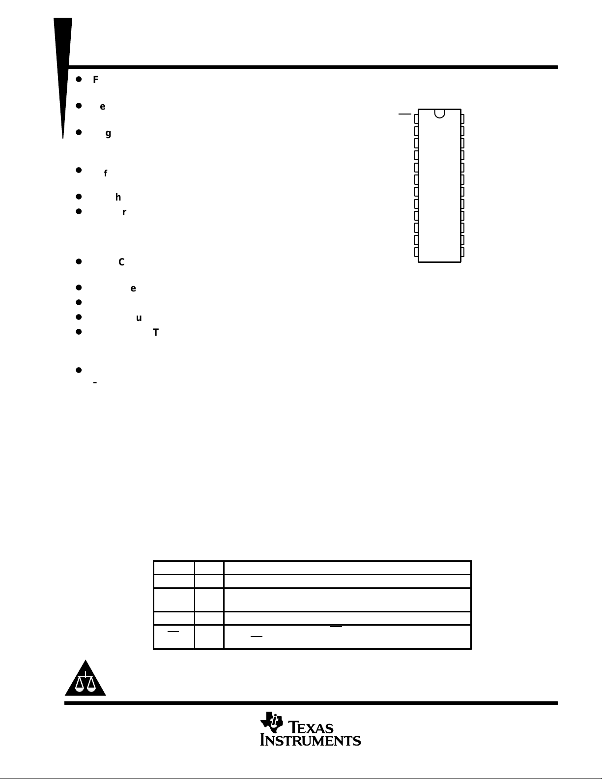
CY54FCT841T ...D PACKAGE
CY74FCT841T ...P, Q, OR SO PACKAGE
OE
D
D
D
D
D
D
D
D
D
D
GND
(TOP VIEW)
1
2
0
3
1
4
2
5
3
6
4
7
5
8
6
9
7
10
8
11
9
12
24
23
22
21
20
19
18
17
16
15
14
13
V
Y
Y
Y
Y
Y
Y
Y
Y
Y
Y
LE
CC
0
1
2
3
4
5
6
7
8
9
description
The ’FCT841T bus-interface latches are designed to eliminate additional packages required to buffer existing
latches and provide additional data width for wider address/data paths or buses carrying parity . The ’FCT841T
devices are buffered 10-bit-wide versions of the FCT373 function.
The ’FCT841T devices’ high-performance interface is designed for high-capacitance-load drive capability , while
providing low-capacitance bus loading at both inputs and outputs. Outputs are designed for low-capacitance
bus loading in the high-impedance state.
These devices are fully specified for partial-power-down applications using I
outputs, preventing damaging current backflow through the device when it is powered down.
PIN DESCRIPTION
NAME
D I Latch data inputs
LE I
Y O 3-state latch outputs
OE I
Please be aware that an important notice concerning availability, standard warranty, and use in critical applications of
Texas Instruments semiconductor products and disclaimers thereto appears at the end of this data sheet.
I/O DESCRIPTION
Latch-enable input. The latches are transparent when LE is high.
Input data is latched on the high-to-low transition.
Output-enable control. When OE is low, the outputs are enabled.
When OE
is high, the outputs are in the high-impedance (off) state.
. The I
off
circuitry disables the
off
PRODUCTION DATA information is current as of publication date.
Products conform to specifications per the terms of Texas Instruments
standard warranty. Production processing does not necessarily include
testing of all parameters.
POST OFFICE BOX 655303 • DALLAS, TEXAS 75265
Copyright 2001, Texas Instruments Incorporated
On products compliant to MIL-PRF-38535, all parameters are tested
unless otherwise noted. On all other products, production
processing does not necessarily include testing of all parameters.
1
CY54FCT841T, CY74FCT841T
SOIC
SO
FCT841C
40°C to 85°C
SOIC
SO
FCT841A
Transparent
10-BIT LATCHES
WITH 3-STATE OUTPUTS
SCCS035A – SEPTEMBER 1994 – REVISED OCTOBER 2001
ORDERING INFORMATION
T
A
°
–
–55°C to 125°C CDIP – D Tube 10 CY54FCT841ATDMB
†
Package drawings, standard packing quantities, thermal data, symbolization, and PCB design guidelines are
available at www.ti.com/sc/package.
°
PACKAGE
QSOP – Q Tape and reel 5.5 CY74FCT841CTQCT FCT841C
–
DIP – P Tube 6.5 CY74FCT841BTPC CY74FCT841BTPC
–
OE LE D O Y
H = High logic level, L = Low logic level, X = Don’t care,
NC = No change, Z = High-impedance state
Tube 5.5 CY74FCT841CTSOC
Tape and reel 5.5 CY74FCT841CTSOCT
Tube 9 CY74FCT841ATSOC
Tape and reel 9 CY74FCT841ATSOCT
INPUTS
H X X X Z
H HLLZZ
H HHHZ
H L X NC Z Latched (Z)
L H L L L
L HHHH
L L X NC NC Latched
†
FUNCTION TABLE
SPEED
(ns)
INTERNAL
OUTPUTS
ORDERABLE
PART NUMBER
FUNCTION
p
TOP-SIDE
MARKING
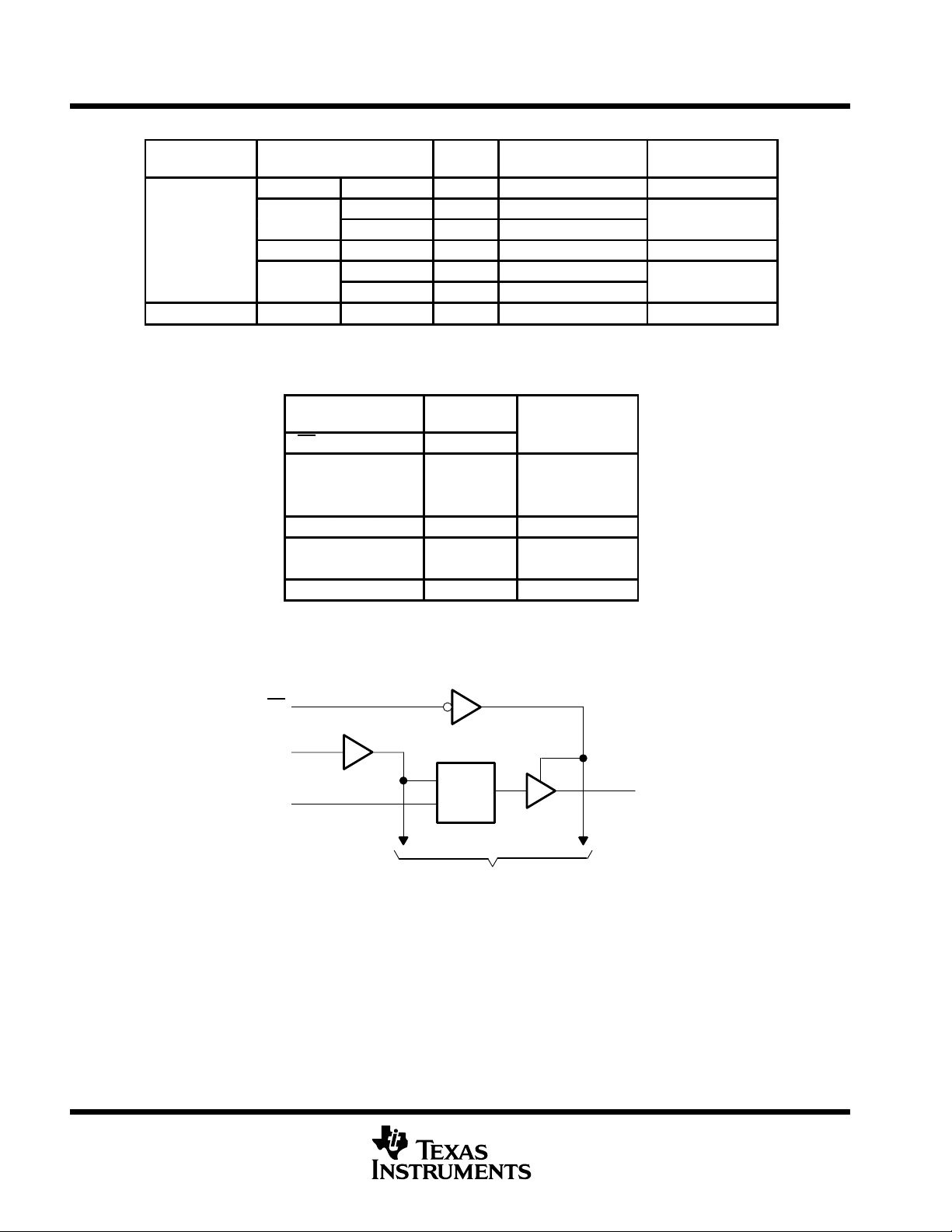
logic diagram (positive logic)
OE
LE
D
0
1
13
2
LE
Q
D
To Nine Other Channels
23
Y
0
2
POST OFFICE BOX 655303 • DALLAS, TEXAS 75265

UNIT
CY54FCT841T, CY74FCT841T
10-BIT LATCHES
WITH 3-STATE OUTPUTS
SCCS035A – SEPTEMBER 1994 – REVISED OCTOBER 2001
absolute maximum ratings over operating free-air temperature range (unless otherwise noted)
Supply voltage range to ground potential –0.5 V to 7 V. . . . . . . . . . . . . . . . . . . . . . . . . . . . . . . . . . . . . . . . . . . . . .
DC input voltage range –0.5 V to 7 V. . . . . . . . . . . . . . . . . . . . . . . . . . . . . . . . . . . . . . . . . . . . . . . . . . . . . . . . . . . . .
DC output voltage range –0.5 V to 7 V. . . . . . . . . . . . . . . . . . . . . . . . . . . . . . . . . . . . . . . . . . . . . . . . . . . . . . . . . . . .
DC output current (maximum sink current/pin) 120 mA. . . . . . . . . . . . . . . . . . . . . . . . . . . . . . . . . . . . . . . . . . . . . .
Package thermal impedance, θ
(see Note 1): P package 67°C/W. . . . . . . . . . . . . . . . . . . . . . . . . . . . . . . . . .
JA
(see Note 2): Q package 61°C/W. . . . . . . . . . . . . . . . . . . . . . . . . . . . . . . . . .
(see Note 2): SO package 46°C/W. . . . . . . . . . . . . . . . . . . . . . . . . . . . . . . . .
Ambient temperature range with power applied, T
Storage temperature range, T
†
Stresses beyond those listed under “absolute maximum ratings” may cause permanent damage to the device. These are stress ratings only, and
functional operation of the device at these or any other conditions beyond those indicated under “recommended operating conditions” is not
implied. Exposure to absolute-maximum-rated conditions for extended periods may affect device reliability.
NOTES: 1. The package thermal impedance is calculated in accordance with JESD 51-3.
2. The package thermal impedance is calculated in accordance with JESD 51-7.
–65°C to 150°C. . . . . . . . . . . . . . . . . . . . . . . . . . . . . . . . . . . . . . . . . . . . . . . . . . .
stg
–65°C to 135°C. . . . . . . . . . . . . . . . . . . . . . . . . . . . . . . . . . .
A
recommended operating conditions (see Note 3)
CY54FCT841T CY74FCT841T
MIN NOM MAX MIN NOM MAX
V
Supply voltage 4.5 5 5.5 4.75 5 5.25 V
CC
V
High-level input voltage 2 2 V
IH
V
Low-level input voltage 0.8 0.8 V
IL
I
High-level output current –12 –32 mA
OH
I
Low-level output current 32 64 mA
OL
T
Operating free-air temperature –55 125 –40 85 °C
A
NOTE 3: All unused inputs of the device must be held at VCC or GND to ensure proper device operation.
†
POST OFFICE BOX 655303 • DALLAS, TEXAS 75265
3

CY54FCT841T, CY74FCT841T
PARAMETER
TEST CONDITIONS
UNIT
V
V
V
4.75 V
V
V
I
A
I
A
I
A
I
A
I
A
I
‡
mA
I
mA
∆I
mA
I
¶
10-BIT LATCHES
WITH 3-STATE OUTPUTS
SCCS035A – SEPTEMBER 1994 – REVISED OCTOBER 2001
electrical characteristics over recommended operating free-air temperature range (unless
otherwise noted)
CY54FCT841T CY74FCT841T
MIN TYP†MAX MIN TYP†MAX
IK
V
OH
OL
V
hys
I
IH
IL
OZH
OZL
OS
I
off
CC
CC
CCD
†
Typical values are at VCC = 5 V, TA = 25°C.
‡
Not more than one output should be shorted at a time. Duration of short should not exceed one second. The use of high-speed test apparatus
and/or sample-and-hold techniques are preferable to minimize internal chip heating and more accurately reflect operational values. Otherwise,
prolonged shorting of a high output can raise the chip temperature well above normal and cause invalid readings in other parametric tests. In
any sequence of parameter tests, IOS tests should be performed last.
§
Per TTL-driven input (VIN = 3.4 V); all other inputs at VCC or GND
¶
This parameter is derived for use in total power-supply calculations.
VCC = 4.5 V, IIN = –18 mA –0.7 –1.2
VCC = 4.75 V, IIN = –18 mA –0.7 –1.2
VCC = 4.5 V, IOH = –12 mA 2.4 3.3
=
CC
VCC = 4.5 V, IOL = 32 mA 0.3 0.55
VCC = 4.75 V, IOL = 64 mA 0.3 0.55
All inputs 0.2 0.2 V
VCC = 5.5 V, VIN = V
VCC = 5.25 V, VIN = V
VCC = 5.5 V, VIN = 2.7 V ±1
VCC = 5.25 V, VIN = 2.7 V ±1
VCC = 5.5 V, VIN = 0.5 V ±1
VCC = 5.25 V, VIN = 0.5 V ±1
VCC = 5.5 V, V
VCC = 5.25 V, V
VCC = 5.5 V, V
VCC = 5.25 V, V
VCC = 5.5 V, V
VCC = 5.25 V, V
VCC = 0 V, V
VCC = 5.5 V, VIN ≤ 0.2 V, VIN ≥ VCC – 0.2 V 0.1 0.2
VCC = 5.25 V, VIN ≤ 0.2 V, VIN ≥ VCC – 0.2 V 0.1 0.2
VCC = 5.5 V, VIN = 3.4 V§, f1 = 0, Outputs open 0.5 2
VCC = 5.25 V, VIN = 3.4 V§, f1 = 0, Outputs open 0.5 2
VCC = 5.5 V, One input switching at 50% duty cycle,
Outputs open, OE
VIN ≤ 0.2 V or VIN ≥ VCC – 0.2 V
VCC = 5.25 V, One input switching at 50% duty cycle,
Outputs open, OE
VIN ≤ 0.2 V or VIN ≥ VCC – 0.2 V
IOH = –32 mA 2
IOH = –15 mA 2.4 3.3
CC
CC
= 2.7 V 10
OUT
= 2.7 V 10
OUT
= 0.5 V –10
OUT
= 0.5 V –10
OUT
= 0 V –60 –120 –225
OUT
= 0 V –60 –120 –225
OUT
= 4.5 V ±1 ±1 µA
OUT
= GND, LE = VCC,
= GND, LE = VCC,
0.06 0.12
5
5
mA/
MHz
0.06 0.12
V
µ
µ
µ
µ
µ
4
POST OFFICE BOX 655303 • DALLAS, TEXAS 75265

PARAMETER
TEST CONDITIONS
UNIT
V
CC
1
,
1
I
#
mA
V
CC
1
,
1
UNIT
CY54FCT841T, CY74FCT841T
10-BIT LATCHES
WITH 3-STATE OUTPUTS
SCCS035A – SEPTEMBER 1994 – REVISED OCTOBER 2001
electrical characteristics over recommended operating free-air temperature range (unless
otherwise noted) (continued)
CY54FCT841T CY74FCT841T
MIN TYP†MAX MIN TYP†MAX
One bit switching
= 5.5 V,
Outputs open,
OE = GND,
LE = V
CC
C
= 5.25 V,
Outputs open,
OE = GND,
LE = V
CC
C
i
C
o
†
Typical values are at VCC = 5 V, TA = 25°C.
#
I
= ICC + ∆ICC × DH × NT + I
C
Where:
I
= Total supply current
C
I
= Power-supply current with CMOS input levels
CC
∆ICC= Power-supply current for a TTL high input (VIN = 3.4 V)
DH= Duty cycle for TTL inputs high
NT= Number of TTL inputs at D
I
= Dynamic current caused by an input transition pair (HLH or LHL)
CCD
f
= Clock frequency for registered devices, otherwise zero
0
f
= Input signal frequency
1
N1= Number of inputs changing at f
All currents are in milliamperes and all frequencies are in megahertz.
||
Values for these conditions are examples of the ICC formula.
at f1 = 10 MHz
at 50% duty cycle
10 bits switching
at f1 = 2.5 MHz
at 50% duty cycle
One bit switching
at f1 = 10 MHz
at 50% duty cycle
10 bits switching
at f1 = 2.5 MHz
at 50% duty cycle
(f0/2 + f1 × N1)
CCD
H
1
VIN ≤ 0.2 V or
VIN ≥ VCC – 0.2 V
VIN = 3.4 V or GND 1 2.4
VIN ≤ 0.2 V or
VIN ≥ VCC – 0.2 V
VIN = 3.4 V or GND 4.1 13.2
VIN ≤ 0.2 V or
VIN ≥ VCC – 0.2 V
VIN = 3.4 V or GND 1 2.4
VIN ≤ 0.2 V or
VIN ≥ VCC – 0.2 V
VIN = 3.4 V or GND 4.1 13.2
0.7 1.4
1 3.2
5 10 5 10 pF
9 12 9 12 pF
||
||
0.7 1.4
1 3.2
||
||
timing requirements over recommended operating free-air temperature range (unless otherwise
noted) (see Figure 1)
CY54FCT841AT CY74FCT841AT CY74FCT841BT CY74FCT841CT
MIN MAX MIN MAX MIN MAX MIN MAX
t
Pulse duration, LE high 5 4 4 4 ns
w
t
Setup time, data before LE↑ 2.5 2.5 2.5 2.5 ns
su
t
Hold time, data after LE↑ 3 2.5 2.5 2.5 ns
h
POST OFFICE BOX 655303 • DALLAS, TEXAS 75265
5

CY54FCT841T, CY74FCT841T
PARAMETER
TEST LOAD
UNIT
D
Y
L
,
ns
D
Y
L
,
ns
LE
Y
L
,
ns
LE
Y
L
,
ns
OE
Y
L
,
ns
OE
Y
L
,
ns
OE
Y
L
,
ns
OE
Y
L
ns
PARAMETER
TEST LOAD
UNIT
D
Y
L
,
ns
D
Y
L
,
ns
LE
Y
L
,
ns
LE
Y
L
,
ns
OE
Y
L
,
ns
OE
Y
L
,
ns
OE
Y
L
,
ns
OE
Y
L
ns
10-BIT LATCHES
WITH 3-STATE OUTPUTS
SCCS035A – SEPTEMBER 1994 – REVISED OCTOBER 2001
switching characteristics over operating free-air temperature range (see Figure 1)
CY54FCT841AT CY74FCT841AT
MIN MAX MIN MAX
1.5 10 1.5 9
1.5 10 1.5 9
1.5 15 1.5 13
1.5 15 1.5 13
1.5 13 1.5 12
1.5 13 1.5 12
1.5 20 1.5 16
1.5 20 1.5 16
1.5 13 1.5 11.5
1.5 13 1.5 11.5
1.5 25 1.5 23
1.5 25 1.5 23
1.5 9 1.5 7
1.5 9 1.5 7
1.5 10 1.5 8
1.5 10 1.5 8
t
PLH
t
PHL
t
PLH
t
PHL
t
PLH
t
PHL
t
PLH
t
PHL
t
PZH
t
PZL
t
PZH
t
PZL
t
PHZ
t
PLZ
t
PHZ
t
PLZ
FROM TO
(INPUT) (OUTPUT)
C
= 50 pF,
RL = 500 Ω
C
= 300 pF,
RL = 500 Ω
C
= 50 pF,
RL = 500 Ω
C
= 300 pF,
RL = 500 Ω
C
= 50 pF,
RL = 500 Ω
C
= 300 pF,
RL = 500 Ω
C
= 5 pF,
RL = 500 Ω
CL = 50 pF,
RL = 500 Ω
switching characteristics over operating free-air temperature range (see Figure 1)
CY74FCT841BT CY74FCT841CT
MIN MAX MIN MAX
1.5 6.5 1.5 5.5
1.5 6.5 1.5 5.5
1.5 13 1.5 13
1.5 13 1.5 13
1.5 8 1.5 6.4
1.5 8 1.5 6.4
1.5 15.5 1.5 15
1.5 15.5 1.5 15
1.5 8 1.5 6.5
1.5 8 1.5 6.5
1.5 14 1.5 12
1.5 14 1.5 12
1.5 6 1.5 5.7
1.5 6 1.5 5.7
1.5 7 1.5 6
1.5 7 1.5 6
t
PLH
t
PHL
t
PLH
t
PHL
t
PLH
t
PHL
t
PLH
t
PHL
t
PZH
t
PZL
t
PZH
t
PZL
t
PHZ
t
PLZ
t
PHZ
t
PLZ
FROM TO
(INPUT) (OUTPUT)
C
= 50 pF,
RL = 500 Ω
C
= 50 pF,
RL = 500 Ω
C
= 50 pF,
RL = 500 Ω
C
= 300 pF,
RL = 500 Ω
C
= 50 pF,
RL = 500 Ω
C
= 300 pF,
RL = 500 Ω
C
= 5 pF,
RL = 500 Ω
CL = 50 pF
RL = 500 Ω,
6
POST OFFICE BOX 655303 • DALLAS, TEXAS 75265

From Output
Under Test
CL = 50 pF
(see Note A)
Test
Point
500 Ω
CY54FCT841T, CY74FCT841T
SCCS035A – SEPTEMBER 1994 – REVISED OCTOBER 2001
PARAMETER MEASUREMENT INFORMATION
7 V
From Output
Under Test
CL = 50 pF
(see Note A)
500 Ω
500 Ω
S1
Open
GND
10-BIT LATCHES
WITH 3-STATE OUTPUTS
TEST S1
t
PLH/tPHL
t
PLZ/tPZL
t
PHZ/tPZH
Open
7 V
Open
LOAD CIRCUIT FOR
TOTEM-POLE OUTPUTS
t
w
Input
VOLTAGE WAVEFORMS
PULSE DURATION
Input
t
PLH
In-Phase
Output
t
PHL
Out-of-Phase
Output
PROPAGATION DELAY TIMES
INVERTING AND NONINVERTING OUTPUTS
NOTES: A. CL includes probe and jig capacitance.
B. Waveform 1 is for an output with internal conditions such that the output is low except when disabled by the output control.
Waveform 2 is for an output with internal conditions such that the output is high except when disabled by the output control.
C. The outputs are measured one at a time with one input transition per measurement.
1.5 V 1.5 V
1.5 V 1.5 V
1.5 V 1.5 V
VOLTAGE WAVEFORMS
1.5 V1.5 V
LOAD CIRCUIT FOR
3-STATE OUTPUTS
3 V
0 V
3 V
0 V
t
PHL
V
OH
V
OL
t
PLH
V
OH
V
OL
Timing Input
Data Input
Output
Control
Output
Waveform 1
(see Note B)
Output
Waveform 2
(see Note B)
1.5 V
t
t
su
VOLTAGE WAVEFORMS
SETUP AND HOLD TIMES
1.5 V 1.5 V
t
PZL
1.5 V
t
PZH
1.5 V
VOLTAGE WAVEFORMS
ENABLE AND DISABLE TIMES
LOW- AND HIGH-LEVEL ENABLING
h
1.5 V1.5 V
VOL + 0.3 V
VOH – 0.3 V
t
PLZ
t
PHZ
3 V
0 V
3 V
0 V
3 V
0 V
≈3.5 V
V
OL
V
OH
≈0 V
Figure 1. Load Circuit and Voltage Waveforms
POST OFFICE BOX 655303 • DALLAS, TEXAS 75265
7

PACKAGE OPTION ADDENDUM
www.ti.com
12-Jan-2006
PACKAGING INFORMATION
Orderable Device Status
(1)
Package
Type
Package
Drawing
Pins Package
Qty
Eco Plan
5962-88575013A ACTIVE LCCC FK 28 1 TBD Call TI N / A for Pkg Type
CY54FCT841ATDMB ACTIVE CDIP JT 24 1 TBD Call TI N / Afor Pkg Type
CY54FCT841ATLMB ACTIVE LCCC FK 28 1 TBD Call TI N / A for PkgType
CY74FCT841ATSOC ACTIVE SOIC DW 24 25 Green (RoHS &
no Sb/Br)
CY74FCT841ATSOCE4 ACTIVE SOIC DW 24 25 Green (RoHS &
no Sb/Br)
CY74FCT841ATSOCT ACTIVE SOIC DW 24 2000 Green(RoHS &
no Sb/Br)
CY74FCT841ATSOCTE4 ACTIVE SOIC DW 24 2000 Green (RoHS&
no Sb/Br)
CY74FCT841BTPC ACTIVE PDIP NT 24 15 Pb-Free
CY74FCT841BTPCE4 ACTIVE PDIP NT 24 15 Pb-Free
CY74FCT841CTQCT ACTIVE SSOP/
QSOP
CY74FCT841CTQCTE4 ACTIVE SSOP/
QSOP
DBQ 24 2500 Green(RoHS &
no Sb/Br)
DBQ 24 2500 Green(RoHS &
no Sb/Br)
CY74FCT841CTSOC ACTIVE SOIC DW 24 25 Green (RoHS &
no Sb/Br)
CY74FCT841CTSOCE4 ACTIVE SOIC DW 24 25 Green (RoHS &
no Sb/Br)
CY74FCT841CTSOCT ACTIVE SOIC DW 24 2000 Green (RoHS&
no Sb/Br)
CY74FCT841CTSOCTE4 ACTIVE SOIC DW 24 2000 Green(RoHS &
no Sb/Br)
(1)
The marketing status valuesare defined as follows:
ACTIVE: Product device recommendedfor new designs.
LIFEBUY: TI has announcedthat the device will be discontinued, and a lifetime-buy period is in effect.
NRND: Not recommended for new designs. Device is in production to support existing customers, but TI does not recommend using this part in
a new design.
PREVIEW: Device has beenannounced but is not in production. Samples may or may not be available.
OBSOLETE: TI has discontinuedthe production of the device.
(RoHS)
(RoHS)
(2)
Lead/Ball Finish MSL Peak Temp
CU NIPDAU Level-1-260C-UNLIM
CU NIPDAU Level-1-260C-UNLIM
CU NIPDAU Level-1-260C-UNLIM
CU NIPDAU Level-1-260C-UNLIM
CU NIPDAU N / A for Pkg Type
CU NIPDAU N / A for Pkg Type
CU NIPDAU Level-2-260C-1YEAR
CU NIPDAU Level-2-260C-1YEAR
CU NIPDAU Level-1-260C-UNLIM
CU NIPDAU Level-1-260C-UNLIM
CU NIPDAU Level-1-260C-UNLIM
CU NIPDAU Level-1-260C-UNLIM
(3)
(2)
Eco Plan - The planned eco-friendly classification: Pb-Free (RoHS), Pb-Free (RoHS Exempt), or Green (RoHS & no Sb/Br) - please check
http://www.ti.com/productcontent for the latestavailability information and additional product content details.
TBD: The Pb-Free/Green conversionplan has not been defined.
Pb-Free (RoHS): TI's terms "Lead-Free" or "Pb-Free" mean semiconductor products that are compatible with the current RoHS requirements
for all 6 substances, including the requirement that lead not exceed 0.1% by weight in homogeneous materials. Where designed to be soldered
at high temperatures, TIPb-Free products are suitable for use in specified lead-free processes.
Pb-Free (RoHS Exempt): This component has a RoHS exemption for either 1) lead-based flip-chip solder bumps used between the die and
package, or 2) lead-based die adhesive used between the die and leadframe. The component is otherwise considered Pb-Free (RoHS
compatible) as defined above.
Green (RoHS & no Sb/Br): TI defines "Green" to mean Pb-Free (RoHS compatible), and free of Bromine (Br) and Antimony (Sb) based flame
retardants (Br or Sbdo not exceed 0.1% by weight in homogeneous material)
(3)
MSL, Peak Temp. -- The Moisture Sensitivity Level rating according to the JEDEC industry standard classifications, and peak solder
temperature.
Important Information and Disclaimer:The information provided on this page represents TI's knowledge and belief as of the date that it is
provided. TI bases its knowledge and belief on information provided by third parties, and makes no representation or warranty as to the
Addendum-Page 1

PACKAGE OPTION ADDENDUM
www.ti.com
accuracy of such information. Efforts are underway to better integrate information from third parties. TI has taken and continues to take
reasonable steps to provide representative and accurate information but may not have conducted destructive testing or chemical analysis on
incoming materials and chemicals. TI and TI suppliers consider certain information to be proprietary, and thus CAS numbers and other limited
information may not beavailable for release.
In no event shall TI's liability arising out of such information exceed the total purchase price of the TI part(s) at issue in this document sold by TI
to Customer on anannual basis.
12-Jan-2006
Addendum-Page 2

IMPORTANT NOTICE
Texas Instruments Incorporated and its subsidiaries (TI) reserve the right to make corrections, modifications,
enhancements, improvements, and other changes to its products and services at any time and to discontinue
any product or service without notice. Customers should obtain the latest relevant information before placing
orders and should verify that such information is current and complete. All products are sold subject to TI’s terms
and conditions of sale supplied at the time of order acknowledgment.
TI warrants performance of its hardware products to the specifications applicable at the time of sale in
accordance with TI’s standard warranty. Testing and other quality control techniques are used to the extent TI
deems necessary to support this warranty. Except where mandated by government requirements, testing of all
parameters of each product is not necessarily performed.
TI assumes no liability for applications assistance or customer product design. Customers are responsible for
their products and applications using TI components. To minimize the risks associated with customer products
and applications, customers should provide adequate design and operating safeguards.
TI does not warrant or represent that any license, either express or implied, is granted under any TI patent right,
copyright, mask work right, or other TI intellectual property right relating to any combination, machine, or process
in which TI products or services are used. Information published by TI regarding third-party products or services
does not constitute a license from TI to use such products or services or a warranty or endorsement thereof.
Use of such information may require a license from a third party under the patents or other intellectual property
of the third party, or a license from TI under the patents or other intellectual property of TI.
Reproduction of information in TI data books or data sheets is permissible only if reproduction is without
alteration and is accompanied by all associated warranties, conditions, limitations, and notices. Reproduction
of this information with alteration is an unfair and deceptive business practice. TI is not responsible or liable for
such altered documentation.
Resale of TI products or services with statements different from or beyond the parameters stated by TI for that
product or service voids all express and any implied warranties for the associated TI product or service and
is an unfair and deceptive business practice. TI is not responsible or liable for any such statements.
Following are URLs where you can obtain information on other Texas Instruments products and application
solutions:
Products Applications
Amplifiers amplifier.ti.com Audio www.ti.com/audio
Data Converters dataconverter.ti.com Automotive www.ti.com/automotive
DSP dsp.ti.com Broadband www.ti.com/broadband
Interface interface.ti.com Digital Control www.ti.com/digitalcontrol
Logic logic.ti.com Military www.ti.com/military
Power Mgmt power.ti.com Optical Networking www.ti.com/opticalnetwork
Microcontrollers microcontroller.ti.com Security www.ti.com/security
Telephony www.ti.com/telephony
Video & Imaging www.ti.com/video
Wireless www.ti.com/wireless
Mailing Address: Texas Instruments
Post Office Box 655303 Dallas, Texas 75265
Copyright 2006, Texas Instruments Incorporated
 Loading...