

Page 1
0 5 10 15 20 25
40
50
60
70
80
90
100
0
2
4
6
8
10
12
Output Current (A)
Efficiency (%)
Power Loss (W)
VGS = 5V
VIN = 12V
V
OUT
= 1.8V
L
OUT
= .29µH
f
S
W
= 500kHz
TA = 25ºC
G001
CSD97374Q4M
Not Recommended For New Designs
www.ti.com
SLPS382C –JANUARY 2013–REVISED JULY 2013
Synchronous Buck NexFET™ Power Stage
1
FEATURES APPLICATIONS
23
• Over 92% System Efficiency at 15A • Ultrabook/Notebook DC/DC Converters
• Max Rated Continuous Current 25A, Peak 60A • Multiphase Vcore and DDR Solutions
• High Frequency Operation (up to 2 MHz) • Point-of-Load Synchronous Buck in
• High Density - SON 3.5x4.5-mm Footprint
• Ultra Low Inductance Package
• System Optimized PCB Footprint
• Ultra Low Quiescent (ULQ) Current Mode
• 3.3V and 5V PWM Signal Compatible
• Diode Emulation Mode with FCCM
• Input Voltages up to 24V
• Three-State PWM Input
• Integrated Bootsrap Diode
• Shoot Through Protection
• RoHS Compliant – Lead Free Terminal Plating
• Halogen Free
Networking, Telecom, and Computing Systems
ORDERING INFORMATION
Device Package Media Qty Ship
CSD97374Q4M 2500
SON 3.5 × 4.5-mm 13-Inch Tape and
Plastic Package Reel Reel
DESCRIPTION
The CSD97374Q4M NexFET™ Power Stage is a highly optimized design for use in a high power, high density
Synchronous Buck converter. This product integrates the driver IC and NexFET technology to complete the
power stage switching function. The driver IC has a built-in selectable diode emulation function that enables
DCM operation to improve light load efficiency. In addition, the driver IC supports ULQ mode that enables
Connected Standby for Windows™ 8 . With the PWM input in tri-state, quiescent current is reduced to 130 µA,
with immediate response. When SKIP# is held at tri-state, the current is reduced to 8 µA (typically 20 µs is
required to resume switching). This combination produces a high current, high efficiency, and high speed
switching device in a small 3.5 × 4.5-mm outline package. In addition, the PCB footprint has been optimized to
help reduce design time and simplify the completion of the overall system design.
1
2NexFET is a trademark of Texas Instruments.
3All other trademarks are the property of their respective owners.
PRODUCTION DATA information is current as of publication date.
Products conform to specifications per the terms of the Texas
Instruments standard warranty. Production processing does not
necessarily include testing of all parameters.
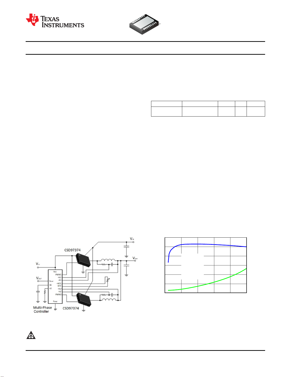
Figure 1. Application Diagram Figure 2. Efficiency and Power Loss
Please be aware that an important notice concerning availability, standard warranty, and use in critical applications of
Texas Instruments semiconductor products and disclaimers thereto appears at the end of this data sheet.
Copyright © 2013, Texas Instruments Incorporated
Page 2
CSD97374Q4M
Not Recommended For New Designs
SLPS382C –JANUARY 2013–REVISED JULY 2013
These devices have limited built-in ESD protection. The leads should be shorted together or the device placed in conductive foam
during storage or handling to prevent electrostatic damage to the MOS gates.
www.ti.com
ABSOLUTE MAXIMUM RATINGS
(1)
TA= 25°C (unless otherwise noted)
VALUE
MIN MAX
VINto P
GND
VSWto P
VSWto P
VDDto P
, VINto V
GND
, VINto VSW(<10ns) -7 33 V
GND
GND
PWM, SKIP# to P
BOOT to P
BOOT to P
GND
(<10ns) -2 38 V
GND
SW
GND
-0.3 30 V
-0.3 30 V
–0.3 6 V
–0.3 6 V
–0.3 35 V
BOOT to BOOT_R –0.3 6 V
ESD Rating
Power Dissipation, P
Operating Temperature Range, T
Storage Temperature Range, T
Human Body Model (HBM) 2000 V
Charged Device Model (CDM) 500 V
D
J
STG
-40 150 °C
–55 150 °C
8 W
(1) Stresses above those listed in "Absolute Maximum Ratings" may cause permanent damage to the device. These are stress ratings only
and functional operation of the device at these or any other conditions beyond those indicated under "Recommended Operating
Conditions" is not implied. Exposure to Absolute Maximum rated conditions for extended periods may affect device reliability.
UNIT
RECOMMENDED OPERATING CONDITIONS
TA= 25° (unless otherwise noted)
Parameter Conditions MIN MAX UNIT
Gate Drive Voltage, V
Input Supply Voltage, V
Continuous Output Current, I
Peak Output Current, I
Switching Frequency, f
DD
IN
OUT-PK
SW
OUT
(2)
VIN= 12V, VDD= 5V, V
fSW= 500kHz, L
C
= 0.1µF (min) 2000 kHz
BST
OUT
= 1.8V, 25 A
OUT
= 0.29µH
(1)
On Time Duty Cycle 85 %
Minimum PWM On Time 40 ns
Operating Temperature –40 125 °C
(1) Measurement made with six 10-µF (TDK C3216X5R1C106KT or equivalent) ceramic capacitors placed across VINto P
(2) System conditions as defined in Note 1. Peak Output Current is applied for tp= 10ms, duty cycle ≤ 1%
4.5 5.5 V
24 V
60 A
pins.
GND
THERMAL INFORMATION
TA= 25°C (unless otherwise noted)
R
θJC
R
θJB
(1) R
(2) R
2 Submit Documentation Feedback Copyright © 2013, Texas Instruments Incorporated
Thermal Resistance, Junction-to-Case (Top of package)
Thermal Resistance, Junction-to-Board
is determined with the device mounted on a 1-inch² (6.45 -cm²), 2-oz (.071-mm thick) Cu pad on a 1.5-inch x 1.5-inch, 0.06-inch
θJC
(1.52-mm) thick FR4 board.
value based on hottest board temperature within 1mm of the package.
θJB
PARAMETER MIN TYP MAX UNIT
(1)
(2)
22.8 °C/W
2.5 °C/W
Page 3
CSD97374Q4M
Not Recommended For New Designs
www.ti.com
ELECTRICAL CHARACTERISTICS
TA= 25°C, VDD= POR to 5.5V (unless otherwise noted)
PARAMETER CONDITIONS MIN TYP MAX UNIT
P
LOSS
Power Loss
Power Loss
Power Loss
V
IN
VINQuiescent Current, I
V
DD
(1)
(2)
(2)
Q
Standby Supply Current, I
Operating Supply Current, I
DD
DD
VIN= 12V, VDD= 5V, V
fSW= 500kHz, L
OUT
VIN= 19V, VDD= 5V, V
fSW= 500kHz, L
OUT
VIN= 19V, VDD= 5V, V
fSW= 500kHz, L
OUT
PWM=Floating, VDD= 5V, VIN= 24V 1 µA
PWM = Float, SKIP# = VDDor 0V 130 µA
SKIP# = Float 8 µA
PWM = 50% Duty cycle, fSW= 500kHz 8.2 mA
POWER-ON RESET AND UNDER VOLTAGE LOCKOUT
Power-On Reset, VDDRising 4.15 V
UVLO, VDDFalling 3.7 V
Hysteresis 0.2 mV
PWM and SKIP# I/O Specifications
Input Impedance, R
Logic Level High, V
Logic Level Low, V
Hysteresis, V
IH
Tri-State Voltage, V
I
IH
IL
TS
Pull Down (to GND) 800
Pull Up to V
DD
Tri-state Activation Time (falling) PWM,
t
THOLD(off1)
Tri-state Activation Time (rising) PWM,
t
THOLD(off2)
Tri-state Activation Time (falling) SKIP#,
t
TSKF
Tri-state Activation Time (rising) SKIP#,
t
TSKR
Tri-state Exit Time PWM, t
Tri-state Exit Time SKIP#, t
3RD(PWM)
3RD(SKIP#)
(2)
(2)
BOOTSTRAP SWITCH
Forward Voltage, V
Reverse Leakage, I
FBST
RLEAK
(2)
IF= 10mA 120 240 mV
V
– VDD= 25V 2 µA
BST
= 1.8V, I
OUT
OUT
= 0.29µH , TJ= 25°C
= 1.8V, I
OUT
OUT
= 0.29µH , TJ= 25°C
= 1.8V, I
OUT
OUT
= 0.29µH , TJ= 125°C
SLPS382C –JANUARY 2013–REVISED JULY 2013
= 15A,
= 15A,
= 15A,
2.3 W
2.5 W
2.8 W
1700
2.65
0.2
1.3 2
60
60
1
1
0.6
100 ns
50 µs
kΩ
V
ns
µs
(1) Measurement made with six 10-µF (TDK C3216X5R1C106KT or equivalent) ceramic capacitors placed across VINto P
(2) Specified by design
Copyright © 2013, Texas Instruments Incorporated Submit Documentation Feedback 3
GND
pins.
Page 4
0 400 800 1200 1600 2000 2400
0.95
1
1.05
1.1
1.15
1.2
1.25
1.3
1.35
1.4
1.45
−0.9
0.0
0.9
1.8
2.7
3.5
4.4
5.3
6.2
7.1
8.0
Switching Frequency (kHz)
Power Loss, Normalized
SOA Temperature Adj (ºC)
VIN = 12V
VDD = 5V
V
OUT
= 1.8V
L
OUT
= 0.29µH
I
OUT
= 25A
G001
3 5 7 9 11 13 15 17 19 21 23
0.95
1
1.05
1.1
1.15
1.2
1.25
−0.9
0.0
0.9
1.8
2.7
3.5
4.4
Input Voltage (V)
Power Loss, Normalized
SOA Temperature Adj (ºC)
VDD = 5V
V
OUT
= 1.8V
L
OUT
= 0.29µH
fSW = 500kHz
I
OUT
= 25A
G001
0
5
10
15
20
25
30
0
10 20 30 40 50 60 70 80 90
Ambient Temperature (ºC)
Output Current (A)
400LFM
200LFM
100LFM
Nat Conv
VIN = 12V
VGS = 5V
V
OUT
= 1.8V
f
S
W
= 500kHz
L
OUT
= 0.29µH
G001
0
5
10
15
20
25
30
0
20 40 60 80 100 120 140
Board Temperature (ºC)
Output Current (A)
Typ
Max
VIN = 12V
VDD = 5V
V
OUT
= 1.8V
f
S
W
= 500kHz
L
OUT
= 0.29µH
G001
0
1
2
3
4
5
6
7
8
9
1
3 5 7 9 11 13 15 17 19 21 23 25
Output Current (A)
Power Loss (W)
Typ
Max
VIN = 12V
VDD = 5V
V
OUT
= 1.8V
fSW = 500kHz
L
OUT
= 0.29µH
G001
0.5
0.6
0.7
0.8
0.9
1
1.1
1.2
−75
−50 −25 0 25 50 75 100 125 150
Junction Temperature (ºC)
Power Loss, Normalized
VIN = 12V
VGS = 5V
V
OUT
= 1.8V
fSW = 500kHz
L
OUT
= 0.29µH
G001
CSD97374Q4M
Not Recommended For New Designs
SLPS382C –JANUARY 2013–REVISED JULY 2013
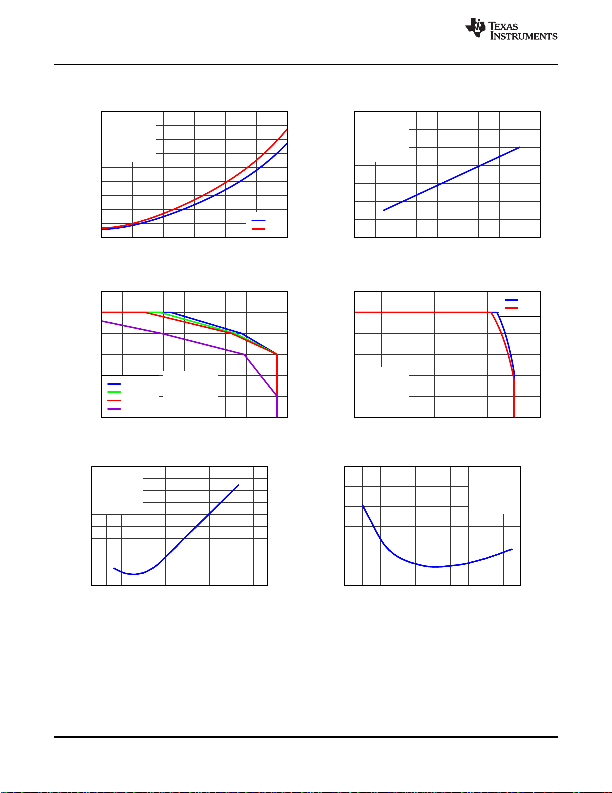
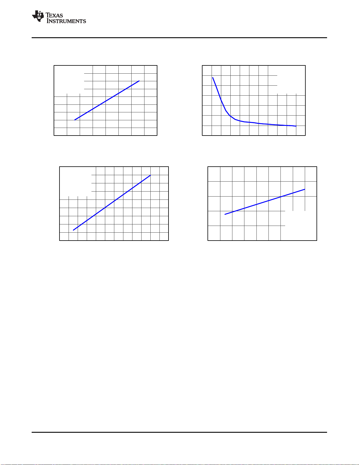
Figure 3. Power Loss vs Output Current Figure 4. Power Loss vs Temperature
www.ti.com
TYPICAL CHARACTERISTICS
TJ= 125°C, unless stated otherwise.
Figure 5. Safe Operating Area – PCB Horizontal Mount
Figure 7. Normalized Power Loss vs Frequency Figure 8. Normalized Power Loss vs Input Voltage
4 Submit Documentation Feedback Copyright © 2013, Texas Instruments Incorporated
(1)
Figure 6. Typical Safe Operating Area
(1)
Page 5
0
5
10
15
20
25
30
35
40
45
0
400 800 1200 1600 2000 2400
Switching Frequency (kHz)
Driver Current (mA)
VIN = 12V
VDD = 5V
V
OUT
= 1.8V
L
OUT
= 0.29µH
I
OUT
= 25A
G000
8.5
9
9.5
10
10.5
11
−75
−50 −25 0 25 50 75 100 125 150
Junction Temperature (°C)
Driver Current (mA)
VIN = 12V
VDD = 5V
V
OUT
= 1.8V
L
OUT
= 0.29µH
I
OUT
= 25A
G000
0 0.5 1 1.5 2 2.5 3 3.5 4
0.6
0.7
0.8
0.9
1
1.1
1.2
1.3
1.4
1.5
−7.2
−5.4
−3.6
−1.8
0
1.8
3.6
5.4
7.2
9
Output Voltage (V)
Power Loss, Normalized
SOA Temperature Adj (ºC)
VIN = 12V
VDD = 5V
fSW = 500kHz
L
OUT
= 0.29µH
I
OUT
= 25A
G001
0 100 200 300 400 500 600 700 800 900 10001100
0.9
0.95
1
1.05
1.1
1.15
1.2
1.25
−1.8
−0.9
0
0.9
1.8
2.7
3.5
4.4
Output Inductance (nH)
Power Loss, Normalized
SOA Temperature Adj (ºC)
VIN = 12V
VDD = 5V
V
OUT
= 1.8V
fSW = 500kHz
I
OUT
= 25A
G001
www.ti.com
Not Recommended For New Designs
TJ= 125°C, unless stated otherwise.
Figure 9. Normalized Power Loss vs Output Voltage Figure 10. Normalized Power Loss vs Output Inductance
CSD97374Q4M
SLPS382C –JANUARY 2013–REVISED JULY 2013
TYPICAL CHARACTERISTICS (continued)
Figure 11. Driver Current vs Frequency Figure 12. Driver Current vs Temperature
1. The Typical CSD97374Q4M System Characteristic curves are based on measurements made on a PCB design with
dimensions of 4.0" (W) x 3.5" (L) x 0.062" (T) and 6 copper layers of 1 oz. copper thickness. See the Application
Information section for detailed explanation.
Copyright © 2013, Texas Instruments Incorporated Submit Documentation Feedback 5
Page 6
PWM
8
7
6
5
4
9
P
GND
1
V
IN
SKIP#
V
SW
V
DD
P
GND
BOOT
BOOT_R
2
3
CSD97374Q4M
Not Recommended For New Designs
SLPS382C –JANUARY 2013–REVISED JULY 2013
PIN CONFIGURATION
Figure 13. Top View
PIN DESCRIPTION
PIN
NO. NAME
1 SKIP# This pin enables the Diode Emulation function. When this pin is held Low, Diode Emulation Mode is enabled for the
Sync FET. When SKIP# is High, the CSD97374Q4M operates in Forced Continuous Conduction Mode. A tri-state
voltage on SKIP# puts the driver into a very low power state.
2 V
DD
3 P
GND
4 V
SW
5 V
IN
6 BOOT_R
7 BOOT
Supply Voltage to Gate Drivers and internal circuitry.
Power Ground, Needs to be connected to Pin 9 and PCB
Voltage Switching Node – pin connection to the output inductor.
Input Voltage Pin. Connect input capacitors close to this pin.
Bootstrap capacitor connection. Connect a minimum 0.1µF 16V X5R, ceramic cap from BOOT to BOOT_R pins. The
bootstrap capacitor provides the charge to turn on the Control FET. The bootstrap diode is integrated.
8 PWM Pulse Width modulated 3-state input from external controller. Logic Low sets Control FET gate low and Sync FET gate
high. Logic High sets Control FET gate high and Sync FET gate Low. Open or High Z sets both MOSFET gates low if
greater than the 3-State Shutdown Hold-off Time (t
9 P
GND
Power Ground
DESCRIPTION
)
3HT
www.ti.com
6 Submit Documentation Feedback Copyright © 2013, Texas Instruments Incorporated
Page 7
UDG-12218
V
UVLO_H
V
UVLO_L
V
VDD
Driver On
www.ti.com
Not Recommended For New Designs
CSD97374Q4M
SLPS382C –JANUARY 2013–REVISED JULY 2013
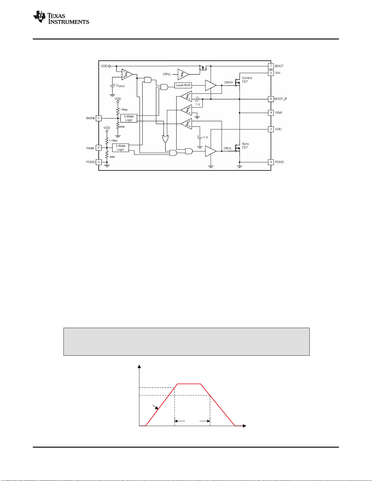
Figure 14. Functional Block Diagram
FUNCTIONAL DESCRIPTION
POWERING CSD97374Q4M AND GATE DRIVERS
An external VDDvoltage is required to supply the integrated gate driver IC and provide the necessary gate drive
power for the MOSFETS. A 1µF 10V X5R or higher ceramic capacitor is recommended to bypass VDDpin to
P
. A bootstrap circuit to provide gate drive power for the Control FET is also included. The bootstrap supply
GND
to drive the Control FET is generated by connecting a 100nF 16V X5R ceramic capacitor between BOOT and
BOOT_R pins. An optional R
resistor can be used to slow down the turn on speed of the Control FET and
BOOT
reduce voltage spikes on the VSWnode. A typical 1Ω to 4.7Ω value is a compromise between switching loss and
VSWspike amplitude.
Undervoltage Lockout Protection (UVLO)
The undervoltage lockout (UVLO) comparator evaluates the VDD voltage level. As V
FET and Sync FET gates hold actively low at all times until V
reaches the higher UVLO threshold (V
VDD
Then the driver becomes operational and responds to PWM and SKIP# commands. If VDD falls below the lower
UVLO threshold (V
UVLO_L
= V
UVLO_H
– Hysteresis), the device disables the driver and drives the outputs of the
Control FET and Sync FET gates actively low. Figure 15 shows this function.
CAUTION
Do not start the driver in the very low power mode (SKIP# = Tri-state).
rises, both the Control
VDD
UVLO_H
).,
Copyright © 2013, Texas Instruments Incorporated Submit Documentation Feedback 7
Figure 15. UVLO Operation
Page 8

CSD97374Q4M
Not Recommended For New Designs
SLPS382C –JANUARY 2013–REVISED JULY 2013
PWM Pin
The PWM pin incorporates an input tri-state function. The device forces the gate driver outputs to low when
PWM is driven into the tri-state window and the driver enters a low power state with zero exit latency. The pin
incorporates a weak pull-up to maintain the voltage within the tri-state window during low-power modes.
Operation into and out of tri-state mode follows the timing diagram outlined in Figure 16.
When VDD reaches the UVLO_H level, a tri-state voltage range (window) is set for the PWM input voltage. The
window is defined the PWM voltage range between PWM logic high (VIH) and logic low (VIL) thresholds. The
device sets high-level input voltage and low-level input voltage threshold levels to accommodate both 3.3 V
(typical) and 5 V (typical) PWM drive signals.
When the PWM exits tri-state, the driver enters CCM for a period of 4 µs, regardless of the state of the SKIP#
pin. Normal operation requires this time period in order for the auto-zero comparator to resume.
www.ti.com
Figure 16. PWM Tri-State Timing Diagram
SKIP# Pin
The SKIP# pin incorporates the input tri-state buffer as PWM. The function is somewhat different. When SKIP# is
low, the zero crossing (ZX) detection comparator is enabled, and DCM mode operation occurs if the load current
is less than the critical current. When SKIP# is high, the ZX comparator disables, and the converter enters FCCM
mode. When both SKIP# and PWM are tri-stated, normal operation forces the gate driver outputs low and the
driver enters a low-power state. In the low-power state, the UVLO comparator remains off to reduce quiescent
current. When SKIP# is pulled low, the driver wakes up and is able to accept PWM pulses in less than 50 µs.
Table 1 shows the logic functions of UVLO, PWM, SKIP#, the Control FET Gate and the Sync FET Gate.
Table 1. Logic Functions of the Driver IC
UVLO PWM SKIP# Sync FET Gate Control FET Gate MODE
Active — — Low Low Disabled
Inactive Low Low High
Inactive Low High High Low FCCM
Inactive High H or L Low High
Inactive Tri-state H or L Low Low LQ
Inactive — Tri-state Low Low ULQ
(1) Until zero crossing protection occurs.
(1)
Low DCM
(1)
8 Submit Documentation Feedback Copyright © 2013, Texas Instruments Incorporated
Page 9

CSD97374Q4M
Not Recommended For New Designs
www.ti.com
Zero Crossing (ZX) Operation
The zero crossing comparator is adaptive for improved accuracy. As the output current decreases from a heavy
load condition, the inductor current also reduces and eventually arrives at a valley, where it touches zero current,
which is the boundary between continuous conduction and discontinuous conduction modes. The SW pin detects
the zero-current condition. When this zero inductor current condition occurs, the ZX comparator turns off the
rectifying MOSFET.
Integrated Boost-Switch
To maintain a BST-SW voltage close to VDD (to get lower conduction losses on the high-side FET), the
conventional diode between the VDD pin and the BST pin is replaced by a FET which is gated by the DRVL
signal.
SLPS382C –JANUARY 2013–REVISED JULY 2013
Copyright © 2013, Texas Instruments Incorporated Submit Documentation Feedback 9
Page 10

CSD97374Q4M
Not Recommended For New Designs
SLPS382C –JANUARY 2013–REVISED JULY 2013
APPLICATION INFORMATION
The Power Stage CSD97374Q4M is a highly optimized design for synchronous buck applications using NexFET
devices with a 5V gate drive. The Control FET and Sync FET silicon are parametrically tuned to yield the lowest
power loss and highest system efficiency. As a result, a rating method is used that is tailored towards a more
systems centric environment. The high-performance gate driver IC integrated in the package helps minimize the
parasitics and results in extremely fast switching of the power MOSFETs. System level performance curves such
as Power Loss, Safe Operating Area and normalized graphs allow engineers to predict the product performance
in the actual application.
Power Loss Curves
MOSFET centric parameters such as R
generated by the devices. In an effort to simplify the design process for engineers, Texas Instruments has
provided measured power loss performance curves. Figure 3 plots the power loss of the CSD97374Q4M as a
function of load current. This curve is measured by configuring and running the CSD97374Q4M as it would be in
the final application (see Figure 17). The measured power loss is the CSD97374Q4M device power loss which
consists of both input conversion loss and gate drive loss. Equation 1 is used to generate the power loss curve.
Power Loss = (VINx IIN) + (VDDx IDD) – (V
The power loss curve in Figure 3 is measured at the maximum recommended junction temperature of
TJ= 125°C under isothermal test conditions.
and Qgdare primarily needed by engineers to estimate the loss
DS(ON)
x I
SW_AVG
) (1)
OUT
Safe Operating Curves (SOA)
The SOA curves in the CSD97374Q4M datasheet give engineers guidance on the temperature boundaries within
an operating system by incorporating the thermal resistance and system power loss. Figure 5 and Figure 6
outline the temperature and airflow conditions required for a given load current. The area under the curve
dictates the safe operating area. All the curves are based on measurements made on a PCB design with
dimensions of 4.0" (W) x 3.5" (L) x 0.062" (T) and 6 copper layers of 1 oz. copper thickness.
www.ti.com
Normalized Curves
The normalized curves in the CSD97374Q4M data sheet give engineers guidance on the Power Loss and SOA
adjustments based on their application specific needs. These curves show how the power loss and SOA
boundaries will adjust for a given set of systems conditions. The primary Y-axis is the normalized change in
power loss and the secondary Y-axis is the change is system temperature required in order to comply with the
SOA curve. The change in power loss is a multiplier for the Power Loss curve and the change in temperature is
subtracted from the SOA curve.
10 Submit Documentation Feedback Copyright © 2013, Texas Instruments Incorporated
Figure 17. Power Loss Test Circuit
Page 11

CSD97374Q4M
Not Recommended For New Designs
www.ti.com
Calculating Power Loss and SOA
The user can estimate product loss and SOA boundaries by arithmetic means (see the Design Example).
Though the Power Loss and SOA curves in this datasheet are taken for a specific set of test conditions, the
following procedure will outline the steps engineers should take to predict product performance for any set of
system conditions.
Design Example
Operating Conditions: Output Current (l
Switching Frequency (fSW) = 800kHz, Output Inductor (L
Calculating Power Loss
• Typical Power Loss at 15A = 2.8W (Figure 3)
• Normalized Power Loss for switching frequency ≈ 1.02 (Figure 7)
• Normalized Power Loss for input voltage ≈ 1.07 (Figure 8)
• Normalized Power Loss for output voltage ≈ 0.94(Figure 9)
• Normalized Power Loss for output inductor ≈ 1.08 (Figure 10)
• Final calculated Power Loss = 2.8W × 1.02 × 1.07 × 0.94 × 1.08 ≈ 3.1W
Calculating SOA Adjustments
• SOA adjustment for switching frequency ≈ 0.3°C (Figure 7)
• SOA adjustment for input voltage ≈ 1.2°C (Figure 8)
• SOA adjustment for output voltage ≈ –1.1°C (Figure 9)
• SOA adjustment for output inductor ≈ 1.4°C (Figure 10)
• Final calculated SOA adjustment = 0.3 + 1.2 + (–1.1) + 1.4 ≈ 1.8°C
) = 15A, Input Voltage (VIN) = 7V, Output Voltage (V
OUT
) = 0.2µH
OUT
SLPS382C –JANUARY 2013–REVISED JULY 2013
) = 1.5V,
OUT
In the design example above, the estimated power loss of the CSD97374Q4M would increase to 3.1W. In
addition, the maximum allowable board and/or ambient temperature would have to decrease by 1.8°C. Figure 18
graphically shows how the SOA curve would be adjusted accordingly.
1. Start by drawing a horizontal line from the application current to the SOA curve.
2. Draw a vertical line from the SOA curve intercept down to the board/ambient temperature.
3. Adjust the SOA board/ambient temperature by subtracting the temperature adjustment value.
In the design example, the SOA temperature adjustment yields a reduction in allowable board/ambient
temperature of 1.8°C. In the event the adjustment value is a negative number, subtracting the negative number
would yield an increase in allowable board/ambient temperature.
Copyright © 2013, Texas Instruments Incorporated Submit Documentation Feedback 11
Figure 18. Power Stage CSD97374Q4M SOA
Page 12

CSD97374Q4M
Not Recommended For New Designs
SLPS382C –JANUARY 2013–REVISED JULY 2013
RECOMMENDED PCB DESIGN OVERVIEW
There are two key system-level parameters that can be addressed with a proper PCB design: electrical and
thermal performance. Properly optimizing the PCB layout will yield maximum performance in both areas. Below
is a brief description on how to address each parameter.
Electrical Performance
The CSD97374Q4M has the ability to switch at voltage rates greater than 10kV/µs. Special care must be then
taken with the PCB layout design and placement of the input capacitors, inductor and output capacitors.
• The placement of the input capacitors relative to VINand P
highest priority during the component placement routine. It is critical to minimize these node lengths. As such,
ceramic input capacitors need to be placed as close as possible to the VINand P
The example in Figure 19 uses 1 x 1nF 0402 25V and 3 x 10µF 1206 25V ceramic capacitors (TDK Part #
C3216X5R1C106KT or equivalent). Notice there are ceramic capacitors on both sides of the board with an
appropriate amount of vias interconnecting both layers. In terms of priority of placement next to the Power
Stage C5, C8 and C6, C19 should follow in order.
• The bootstrap cap C
0.1µF 0603 16V ceramic capacitor should be closely connected between BOOT and
BOOT
BOOT_R pins
• The switching node of the output inductor should be placed relatively close to the Power Stage
CSD97374Q4M VSWpins. Minimizing the VSWnode length between these two components will reduce the
PCB conduction losses and actually reduce the switching noise level.
pins of CSD97374Q4M device should have the
GND
pins (see Figure 19).
GND
(2)
www.ti.com
Thermal Performance
The CSD97374Q4M has the ability to use the GND planes as the primary thermal path. As such, the use of
thermal vias is an effective way to pull away heat from the device and into the system board. Concerns of solder
voids and manufacturability problems can be addressed by the use of three basic tactics to minimize the amount
of solder attach that will wick down the via barrel:
• Intentionally space out the vias from each other to avoid a cluster of holes in a given area.
• Use the smallest drill size allowed in your design. The example in Figure 19 uses vias with a 10 mil drill hole
and a 16 mil capture pad.
• Tent the opposite side of the via with solder-mask.
In the end, the number and drill size of the thermal vias should align with the end user’s PCB design rules and
manufacturing capabilities.
Figure 19. Recommended PCB Layout (Top Down View)
(2) Keong W. Kam, David Pommerenke, “EMI Analysis Methods for Synchronous Buck Converter EMI Root Cause Analysis”, University of
Missouri – Rolla
12 Submit Documentation Feedback Copyright © 2013, Texas Instruments Incorporated
Page 13

1
a1
5
4
c1
8
D2
Ө
°
0.300
(x45°)
www.ti.com
Not Recommended For New Designs
CSD97374Q4M
SLPS382C –JANUARY 2013–REVISED JULY 2013
MECHANICAL DATA
DIM
Min Nom Max Min Nom Max
MILLIMETERS INCHES
A 0.800 0.900 1.000 0.031 0.035 0.039
a1 0.000 0.000 0.080 0.000 0.000 0.003
b 0.150 0.200 0.250 0.006 0.008 0.010
b1 2.000 2.200 2.400 0.079 0.087 0.095
b2 0.150 0.200 0.250 0.006 0.008 0.010
c1 0.150 0.200 0.250 0.006 0.008 0.010
D2 3.850 3.950 4.050 0.152 0.156 0.160
E 4.400 4.500 4.600 0.173 0.177 0.181
E1 3.400 3.500 3.600 0.134 0.138 0.142
E2 2.000 2.100 2.200 0.079 0.083 0.087
e 0.400 TYP 0.016 TYP
K 0.300 TYP 0.012 TYP
L 0.300 0.400 0.500 0.012 0.016 0.020
L1 0.180 0.230 0.280 0.007 0.009 0.011
Copyright © 2013, Texas Instruments Incorporated Submit Documentation Feedback 13
θ 0.00 — — 0.00 — —
Page 14

0.850 (x8)
0.300
0.200 0.200
0.390
0.350
0.225
2.200
0.115
0.738 (x 8)
(0.008) (0.008)
(0.029)
(0.015)
(0.012)
(0.014)
(0.009)
(0.087)
(0.004)
0.400
(0.016)
0.200
(0
.008)
0.300
(0.012)
(0.033)
0.200
(0
.008)
0.440 (0.017)
R0.100
R0.100
0.250
(x18)
(0.010)
0.150
(0.006)
0.600 (x 2)
(0.024)
0.200
(x2)
2.250
0.225 ( x 2)
4.050
2.200
0.300
(0.008)
(0.087)
(0.012)
(0.088)
(0.009)
(0.159)
0.150
(0.006)
0.400
(0.016)
0.440 (0.017)
R0.100
R0.100
CSD97374Q4M
Not Recommended For New Designs
SLPS382C –JANUARY 2013–REVISED JULY 2013
Recommended PCB Land Pattern
www.ti.com
Recommended Stencil Opening
NOTE: Dimensions are in mm (inches).
14 Submit Documentation Feedback Copyright © 2013, Texas Instruments Incorporated
Page 15

CSD97374Q4M
Not Recommended For New Designs
www.ti.com
REVISION HISTORY
Changes from Original (January 2013) to Revision A Page
SLPS382C –JANUARY 2013–REVISED JULY 2013
• Changed the ROC table, From: VSWto P
, VINto VSW(<20ns) MIN = -5 To: VSWto P
GND
, VINto VSW(<10ns) MIN
GND
= -7 ........................................................................................................................................................................................ 2
• Changed the ROC table, From: BOOT to P
(<20ns) MIN = -3 To: BOOT to P
GND
(<10ns) MIN = -2 ............................ 2
GND
• Changed Logic Level High, VIHFrom: MAX = 2.6 To: MIN = 2.65 ....................................................................................... 3
• Changed Logic Level Low, VILFrom: MIN = 0.6 To: MAX = 0.6 .......................................................................................... 3
• Changed Tri-State Voltage, VTSFrom: MIN = 1.2 To: MIN = 1.3 ......................................................................................... 3
Changes from Revision A (March 2013) to Revision B Page
• Changed the Mechanical Drawing image ........................................................................................................................... 13
• Changed the Recommended PCB Land Pattern image ..................................................................................................... 14
• Changed the Recommended Stencil Opening image ........................................................................................................ 14
Changes from Revision B (May 2013) to Revision C Page
• Added dimension row b2 to the MECHANICAL DATA table .............................................................................................. 13
Copyright © 2013, Texas Instruments Incorporated Submit Documentation Feedback 15
Page 16

PACKAGE OPTION ADDENDUM
www.ti.com
PACKAGING INFORMATION
Orderable Device Status
CSD97374Q4M NRND VSON-CLIP DPC 8 2500 Pb-Free (RoHS
FX021 NRND VSON-CLIP DPC 8 2500 Pb-Free (RoHS
(1)
The marketing status values are defined as follows:
ACTIVE: Product device recommended for new designs.
LIFEBUY: TI has announced that the device will be discontinued, and a lifetime-buy period is in effect.
NRND: Not recommended for new designs. Device is in production to support existing customers, but TI does not recommend using this part in a new design.
PREVIEW: Device has been announced but is not in production. Samples may or may not be available.
OBSOLETE: TI has discontinued the production of the device.
Package Type Package
(1)
Drawing
Pins Package
Qty
Eco Plan
(2)
Exempt)
Exempt)
Lead/Ball Finish
(6)
CU NIPDAU Level-2-260C-1 YEAR -40 to 150 97374M
CU NIPDAU Level-2-260C-1 YEAR -40 to 150 97374M
MSL Peak Temp
(3)
Op Temp (°C) Device Marking
(4/5)
(2)
Eco Plan - The planned eco-friendly classification: Pb-Free (RoHS), Pb-Free (RoHS Exempt), or Green (RoHS & no Sb/Br) - please check http://www.ti.com/productcontent for the latest availability
information and additional product content details.
TBD: The Pb-Free/Green conversion plan has not been defined.
Pb-Free (RoHS): TI's terms "Lead-Free" or "Pb-Free" mean semiconductor products that are compatible with the current RoHS requirements for all 6 substances, including the requirement that
lead not exceed 0.1% by weight in homogeneous materials. Where designed to be soldered at high temperatures, TI Pb-Free products are suitable for use in specified lead-free processes.
Pb-Free (RoHS Exempt): This component has a RoHS exemption for either 1) lead-based flip-chip solder bumps used between the die and package, or 2) lead-based die adhesive used between
the die and leadframe. The component is otherwise considered Pb-Free (RoHS compatible) as defined above.
Green (RoHS & no Sb/Br): TI defines "Green" to mean Pb-Free (RoHS compatible), and free of Bromine (Br) and Antimony (Sb) based flame retardants (Br or Sb do not exceed 0.1% by weight
in homogeneous material)
(3)
MSL, Peak Temp. - The Moisture Sensitivity Level rating according to the JEDEC industry standard classifications, and peak solder temperature.
(4)
There may be additional marking, which relates to the logo, the lot trace code information, or the environmental category on the device.
(5)
Multiple Device Markings will be inside parentheses. Only one Device Marking contained in parentheses and separated by a "~" will appear on a device. If a line is indented then it is a continuation
of the previous line and the two combined represent the entire Device Marking for that device.
(6)
Lead/Ball Finish - Orderable Devices may have multiple material finish options. Finish options are separated by a vertical ruled line. Lead/Ball Finish values may wrap to two lines if the finish
value exceeds the maximum column width.
Important Information and Disclaimer:The information provided on this page represents TI's knowledge and belief as of the date that it is provided. TI bases its knowledge and belief on information
provided by third parties, and makes no representation or warranty as to the accuracy of such information. Efforts are underway to better integrate information from third parties. TI has taken and
continues to take reasonable steps to provide representative and accurate information but may not have conducted destructive testing or chemical analysis on incoming materials and chemicals.
TI and TI suppliers consider certain information to be proprietary, and thus CAS numbers and other limited information may not be available for release.
2-Apr-2015
Samples
Addendum-Page 1
Page 17
PACKAGE OPTION ADDENDUM
www.ti.com
In no event shall TI's liability arising out of such information exceed the total purchase price of the TI part(s) at issue in this document sold by TI to Customer on an annual basis.
2-Apr-2015
Addendum-Page 2
Page 18

PACKAGE MATERIALS INFORMATION
www.ti.com 5-Dec-2014
TAPE AND REEL INFORMATION
*All dimensions are nominal
Device Package
CSD97374Q4M VSON-
Type
CLIP
Package
Drawing
Pins SPQ Reel
Diameter
(mm)
DPC 8 2500 330.0 12.4 3.71 4.71 1.1 8.0 12.0 Q1
Reel
Width
W1 (mm)
A0
(mm)B0(mm)K0(mm)P1(mm)W(mm)
Pin1
Quadrant
Pack Materials-Page 1
Page 19

PACKAGE MATERIALS INFORMATION
www.ti.com 5-Dec-2014
*All dimensions are nominal
Device Package Type Package Drawing Pins SPQ Length (mm) Width (mm) Height (mm)
CSD97374Q4M VSON-CLIP DPC 8 2500 367.0 367.0 35.0
Pack Materials-Page 2
Page 20

IMPORTANT NOTICE
Texas Instruments Incorporated and its subsidiaries (TI) reserve the right to make corrections, enhancements, improvements and other
changes to its semiconductor products and services per JESD46, latest issue, and to discontinue any product or service per JESD48, latest
issue. Buyers should obtain the latest relevant information before placing orders and should verify that such information is current and
complete. All semiconductor products (also referred to herein as “components”) are sold subject to TI’s terms and conditions of sale
supplied at the time of order acknowledgment.
TI warrants performance of its components to the specifications applicable at the time of sale, in accordance with the warranty in TI’s terms
and conditions of sale of semiconductor products. Testing and other quality control techniques are used to the extent TI deems necessary
to support this warranty. Except where mandated by applicable law, testing of all parameters of each component is not necessarily
performed.
TI assumes no liability for applications assistance or the design of Buyers’ products. Buyers are responsible for their products and
applications using TI components. To minimize the risks associated with Buyers’ products and applications, Buyers should provide
adequate design and operating safeguards.
TI does not warrant or represent that any license, either express or implied, is granted under any patent right, copyright, mask work right, or
other intellectual property right relating to any combination, machine, or process in which TI components or services are used. Information
published by TI regarding third-party products or services does not constitute a license to use such products or services or a warranty or
endorsement thereof. Use of such information may require a license from a third party under the patents or other intellectual property of the
third party, or a license from TI under the patents or other intellectual property of TI.
Reproduction of significant portions of TI information in TI data books or data sheets is permissible only if reproduction is without alteration
and is accompanied by all associated warranties, conditions, limitations, and notices. TI is not responsible or liable for such altered
documentation. Information of third parties may be subject to additional restrictions.
Resale of TI components or services with statements different from or beyond the parameters stated by TI for that component or service
voids all express and any implied warranties for the associated TI component or service and is an unfair and deceptive business practice.
TI is not responsible or liable for any such statements.
Buyer acknowledges and agrees that it is solely responsible for compliance with all legal, regulatory and safety-related requirements
concerning its products, and any use of TI components in its applications, notwithstanding any applications-related information or support
that may be provided by TI. Buyer represents and agrees that it has all the necessary expertise to create and implement safeguards which
anticipate dangerous consequences of failures, monitor failures and their consequences, lessen the likelihood of failures that might cause
harm and take appropriate remedial actions. Buyer will fully indemnify TI and its representatives against any damages arising out of the use
of any TI components in safety-critical applications.
In some cases, TI components may be promoted specifically to facilitate safety-related applications. With such components, TI’s goal is to
help enable customers to design and create their own end-product solutions that meet applicable functional safety standards and
requirements. Nonetheless, such components are subject to these terms.
No TI components are authorized for use in FDA Class III (or similar life-critical medical equipment) unless authorized officers of the parties
have executed a special agreement specifically governing such use.
Only those TI components which TI has specifically designated as military grade or “enhanced plastic” are designed and intended for use in
military/aerospace applications or environments. Buyer acknowledges and agrees that any military or aerospace use of TI components
which have not been so designated is solely at the Buyer's risk, and that Buyer is solely responsible for compliance with all legal and
regulatory requirements in connection with such use.
TI has specifically designated certain components as meeting ISO/TS16949 requirements, mainly for automotive use. In any case of use of
non-designated products, TI will not be responsible for any failure to meet ISO/TS16949.
Products Applications
Audio www.ti.com/audio Automotive and Transportation www.ti.com/automotive
Amplifiers amplifier.ti.com Communications and Telecom www.ti.com/communications
Data Converters dataconverter.ti.com Computers and Peripherals www.ti.com/computers
DLP® Products www.dlp.com Consumer Electronics www.ti.com/consumer-apps
DSP dsp.ti.com Energy and Lighting www.ti.com/energy
Clocks and Timers www.ti.com/clocks Industrial www.ti.com/industrial
Interface interface.ti.com Medical www.ti.com/medical
Logic logic.ti.com Security www.ti.com/security
Power Mgmt power.ti.com Space, Avionics and Defense www.ti.com/space-avionics-defense
Microcontrollers microcontroller.ti.com Video and Imaging www.ti.com/video
RFID www.ti-rfid.com
OMAP Applications Processors www.ti.com/omap TI E2E Community e2e.ti.com
Wireless Connectivity www.ti.com/wirelessconnectivity
Mailing Address: Texas Instruments, Post Office Box 655303, Dallas, Texas 75265
Copyright © 2015, Texas Instruments Incorporated
Page 21

 Loading...